Embed Size (px)
Citation preview
Studies towards a bio – organic – cell – chip interface
DIPLOMARBEIT
zur Erlangung des akademischen Grades
DIPLOMINGENIEUR
in der Studienrichtung
WIRTSCHAFTSINGENIEURWESEN FÜR CHEMIE
Angefertigt am Linz Institute for Organic Solar Cells (LIOS)
Betreuung:
o. Univ.-Prof. Dr. Serdar N. Sariciftci
Eingereicht von:
Andreas Spiegel
Linz, Oktober 2006
Johannes Kepler Universität A-4040 Linz · Altenbergerstraße 69 · Internet: http://www.uni-linz.ac.at · DVR 0093696

ii
Eidesstattliche Erklärung:
Ich erkläre an Eides statt, dass ich die vorliegende Diplomarbeit selbstständig und ohne
fremde Hilfe verfasst, andere als die angegebenen Quellen und Hilfsmittel nicht benutzt bzw.
die wörtlich oder sinngemäß entnommenen Stellen als solche kenntlich gemacht habe.
Linz, im Oktober 2006
Andreas Spiegel
iii
Abstract
In the course of this work preliminary experiments towards the feasibility of junctions
between cells and electronic devices were performed.
First of all the compatibility of human embryonic kidney (HEK) cells towards a broad range
of untreated organic insulators and organic semiconductor materials was tested.
Based on these results calcium channels were expressed in HEK cells and those should be
stimulated capacitively which didn’t work because the Ca2+ channel couldn’t be expressed
thoroughly in the HEK293 cell culture.
We also looked for a correlation between the adherence of cells to the surface of the dielectric
and the Impedance and Capacitance, respectively.
With the materials which were compatible to the HEK cells we fabricated top gate transistors,
because these seem to be predestined for the role of electronic devices in a cell chip junction.
Zusammenfassung
Im Rahmen dieser Arbeit wurden Voruntersuchungen zur Machbarkeit von Verbindungen
zwischen Zellen und elektronischen Baugruppen wie etwa Transistoren durchgeführt.
Zu diesem Zweck wurde als erster Schritt die Verträglichkeit diverser unbehandelter
organischer Isolatoren und organischer Halbleitermaterialien für Human Embryonic Kidney
(HEK) Zellen getestet.
Aufbauend auf diese Ergebnisse wurde versucht Kalzium - Ionenkanäle von den HEK –
Zellen ausbilden zu lassen und diese dann mittels kapazitiver Stimulation anzuregen, was
daran scheiterte, dass die Ausbildung der Kanäle nicht ausreichend möglich war.
Des Weiteren wurde nach Zusammenhängen zwischen Impedanz bzw. Kapazität und anhaften
von Zellen an der Oberfläche des Isolators gesucht.
Mit den aus den Verträglichkeitsuntersuchungen hervorgegangenen Materialien sollten
außerdem Top – Gate Transistoren gebaut werden, da diese als elektronische Baugruppe für
eine Verbindung mit Zellen prädestiniert sind.

iv
Acknowledgement
The presented work was carried out at the Linz Institute for Organic Solar Cells (LIOS),
Physical Chemistry, Johannes Kepler University Linz, between October 2005 and October
2006.
I want to thank o. Univ. Prof. Dr. Serdar N. Sariciftci for this very interesting topic, guidance
and advice in the last year.
I also like to thank Dr. Birendra Th. Singh for great advice and support.
I thank all present and (former) members of our Institute: Dr. Helmut Neugebauer, (Dr.
Gilles, Dennler), (Dr. Farideh Meghdadi), (Dr. Nenad Marjanović), DI Roppert Koeppe, DI
Christoph Lungenschmied, DI Anita Fuchsbauer, (Dr. Le Huong Nguyen), DI Martin
Egginger, (Dr. Shengli Lu), (DI Hans-Jürgen Prall), Philipp Stadler and Pinar Senkarabacak,
for many fruitful discussions and suggestions, on and off the topic.
Thanks also to our secretaries and technician Petra Neumaier, Birgit Paulik, Erika Bradt,
Gerda Kalab and Manfred Lipp, which help through the bureaucratic problems and supported
me with technical assistance.
Also I’d like to thank the following members of the Biophysics Institute: Dr. Peter Pohl, Dr.
Christoph Romanin, Dr. Klaus Sommer, and especially Sabine Buchegger, who supported me
with healthy HEK293 cells.
I want to thank furthermore my colleagues during the last years of our studies: Cornelia Kock,
Philipp Stadler, Sabrina Heiml, Bernhard Gallistl and Martin Nausner.
Especially I’d like to thank Sabine for supporting me in the last year in every possible way.
Last but not least I’d like to thank my parents for supporting me during the years of my
studies.

v
Für meine Eltern Ernst und Maria Spiegel,
ohne deren Hilfe dieses Studium nicht möglich gewesen wäre.
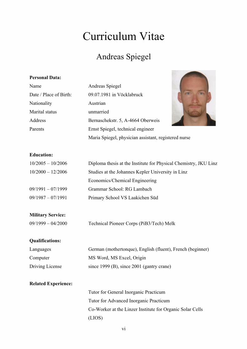
Curriculum Vitae
Andreas Spiegel
Personal Data:
Name Andreas Spiegel
Date / Place of Birth: 09.07.1981 in Vöcklabruck
Nationality Austrian
Marital status unmarried
Address Bernaschekstr. 5, A-4664 Oberweis
Parents Ernst Spiegel, technical engineer
Maria Spiegel, physician assistant, registered nurse
Education:
10/2005 – 10/2006 Diploma thesis at the Institute for Physical Chemistry, JKU Linz
10/2000 – 12/2006 Studies at the Johannes Kepler University in Linz
Economics/Chemical Engineering
09/1991 – 07/1999 Grammar School: RG Lambach
09/1987 – 07/1991 Primary School VS Laakichen Süd
Military Service:
09/1999 – 04/2000 Technical Pioneer Corps (PiB3/Tech) Melk
Qualifications:
Languages German (mothertonque), English (fluent), French (beginner)
Computer MS Word, MS Excel, Origin
Driving License since 1999 (B), since 2001 (gantry crane)
Related Experience:
Tutor for General Inorganic Practicum
Tutor for Advanced Inorganic Practicum
Co-Worker at the Linzer Institute for Organic Solar Cells
(LIOS)
vi
vii
Further Employees:
Summer 1997 Building Yard, Laakirchen
Summer 1998 & 2002 Superintendent at the public swimming pool, Laakirchen
May 2000 Bavarian Red Cross
June/July 2000 Internship at HIPP GmbH, Gmunden, as receptionist
August 2000 Internship at MIBA AG, Laakirchen, galvanization plant
Summer 2001 Internship at UPM Kymmene, Steyrermühl, waste water
Treatment plant
Summer 2003, 2004, 2005: Internship at UPM Kymmene, Steyrermühl paper production
PM3 & PM4
Interests:
Volleyball, Biking, Soccer, Tennis
Contribution to Conferences:
“Study of Ion-selective and bio-functionalised materials for selective field-
effect sensing applications”
A. Spiegel, Th. B. Singh, N.S. Sariciftci, K. Sommer, P. Pohl
E-MRS Spring Meeting, May 2006, Nice (France)

viii
Contents:
1. Motivation .............................................................................................................................. 1
2. Introduction ............................................................................................................................ 3
2.1. Cell-Chip Junction........................................................................................................... 3
2.1.1. Point contact model.................................................................................................. 5
2.1.2. Area contact model................................................................................................... 5
2.2. Signaling in Biology........................................................................................................ 7
2.2.1. The Cell .................................................................................................................... 7
2.2.2. The plasma membrane ............................................................................................. 8
2.2.3. Membrane transport: .............................................................................................. 10
2.3. Signaling in Information Technology ........................................................................... 16
2.3.1. The (organic) capacitor .......................................................................................... 16
2.3.2. Working principle of LCR meter ........................................................................... 17
2.3.3. Organic Semiconductors ........................................................................................ 19
2.3.4. The (organic) field-effect transistor ....................................................................... 20
2.3.5. Operating principle of OFETs................................................................................ 22
3. Experimental ........................................................................................................................ 24
3.1. Compatibility test .......................................................................................................... 24
3.1.1. Sample Preparation ................................................................................................ 24
3.1.2. Sterilization ............................................................................................................ 24
3.1.3. HEK293 cell line.................................................................................................... 24
3.1.4. Cell culturing.......................................................................................................... 25
3.1.5. Tested materials...................................................................................................... 25
3.1.6. Light microscopy.................................................................................................... 29
3.1.7. Pre-treatment of dielectric surfaces........................................................................ 30
3.2. Activation of ion channels in HEK cells ....................................................................... 31
3.2.1. Device Preparation ................................................................................................. 32
3.2.2. Dielectric check...................................................................................................... 33
3.2.3. Transfection............................................................................................................ 33
3.2.4. Imaging................................................................................................................... 35
3.3. Impedance measurements ............................................................................................. 36
3.4. Capacitance Measurement............................................................................................. 36
3.5. I-V Measurements ......................................................................................................... 37

ix
3.6. Top gate transistor ......................................................................................................... 37
3.6.1. Device preparation ................................................................................................. 37
4. Results and Discussion:........................................................................................................ 39
4.1. Results of Compatibility test ......................................................................................... 39
4.1.1. Dielectrics............................................................................................................... 39
4.1.2. Semiconductor materials ........................................................................................ 46
4.2. Activation of ion channels in HEK293 cells ................................................................. 49
4.2.1. Transfection results ................................................................................................ 49
4.3. Impedance measurements ............................................................................................. 52
4.4. Capacitance Measurement............................................................................................. 53
4.4.1. MIM results ............................................................................................................ 53
4.4.2. Capacitance measurement under cell influence ..................................................... 54
4.5. Top gate transistor ......................................................................................................... 55
5. Conclusions .......................................................................................................................... 58
6. References ............................................................................................................................ 59
7. List of Figures ...................................................................................................................... 62
8. Appendix .............................................................................................................................. 65
8.1. Appendix A – Dulbecco’s Modified Eagle Medium (GIBCO) .................................... 65
8.2. Appendix B: Transfection Protocols ............................................................................. 66
8.2.1. Transfection Protocol for TransfectinTM Lipid Reagent by BIO-RAD................... 66
8.2.2. Transfection Protocol for SuperfectTM by Quiagen ............................................... 66
8.2.3. Transfection Protocol for ExGENTM by Fermentas............................................... 66
8.2.4. Transfection Protocol for LipofectaminTM by Invitrogen ...................................... 67
8.3. Appendix C: Used equipment ....................................................................................... 67
1. Motivation Since the rise of information technology or even earlier it has always been a dream for
scientists and science fiction authors to get another interface between computer and user than
the typical keyboard-hand and screen-eye connection.
In fact it was Luigi Galvani (1737-1798) who first interfaced biology and electricity by
accidentally activating frog muscles when one of his assistants touched an exposed nerve in a
dissected frog leg with an electrically charged scalpel which then kicked out [1]. Later his
experiments lead the way to electrochemical cells invented by Alessandro Volta.
After nearly 200 years W. Shockley, J. Bardeen and W. Brattain [2, 3] re-invented the
transistor (J.E. Lilienfeld patented already devices based on the field effect in the year 1930
[4]) in December 1947 in the Bell Labs and earned the Noble Prize for this invention [5]. This
and the invention of the MOSFET (metal oxid semiconductor field-effect transistor) by
Kahng and Attala [6] sub-sequentially started the way among other things to the construction
of computers, which in the beginning were controlled by punch card and later by keyboard
and mouse.
It took another 30 years until E. Neher and B. Sakmann developed Noble Prize wining Patch
Clamp Technology [7], which allows recording and stimulating of Ion channels in cells. A
major disadvantage of this superb tool is that in the course of the measurement the cells have
to be penetrated with a pipette which will lead to the death of the cell.
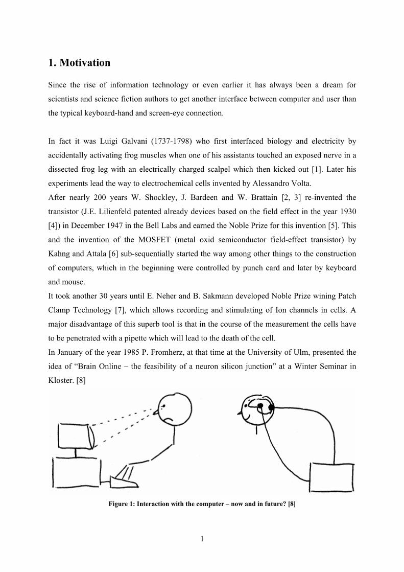
In January of the year 1985 P. Fromherz, at that time at the University of Ulm, presented the
idea of “Brain Online – the feasibility of a neuron silicon junction” at a Winter Seminar in
Kloster. [8]
Figure 1: Interaction with the computer – now and in future? [8]
1
2
Fromherz stated the possibility of exchanging the macroscopically hand keyboard and eye
screen coupling between computer and brain (Figure 1, left) with a direct microscopically
coupling (Figure 1, right).
To realize such a hypothesis, Max Plank Institute for Biophysics with Prof. Peter Fromherz as
the leading scientist, in their pioneering work, used the conventional Silicon and thermally
grown high quality SiO2 based transistors and electronic circuits to grow living cells on. [9]
Since 1977 on the other hand, a class of materials – organic polymers – have been found to be
electrically conducting and they are versatile with respect to their processing and device
fabrication leading a breakthrough in the field of organic electronics. [10, 11, 12, 13]
Since organic polymers are solution processable and have tunable electrical and optical
properties, they are versatile for adaptation to the bio-systems. It is the aim of this thesis to
study the feasibility of Cell growth and Culture, investigate the bio-compatibility using
various types of organic insulators and conducting polymers. This thesis composes of first
hand studies of various organic dielectrics and semiconductors interacting with cells and their
electrical and optical properties.

2. Introduction
2.1. Cell-Chip Junction
In principle the Cell Chip junction can be seen as an interface between mostly ion driven
signaling and electronically driven signaling/signal processing. A direct coupling of ionic
signals in a cell and electronic signals in a microelectronic device can be achieved by
electrical polarization.
When the insulating plasma membrane of the cell is in direct contact with the insulating
dielectric of the device a compact dielectric should be formed. The electrical field of the
polarized cell membrane leads to a polarization of the dielectric which furthermore leads to
the formation of a channel between Source and Drain contact embedded in the Semiconductor
(Figure 2, top). This would be the reading of a signal from the cell or the controlling of the
transistor by the cell.
The other way an electrical field applied to the dielectric of the device (not necessarily a
transistor) leads to a polarization of the plasma membrane which furthermore leads to the
opening of voltage gated ion channels (Figure 2, bottom). This refers to gating of ion channels
by the electronic device.
Cytosol inside the cell Plasma membrane Dielectric Semiconductor S&D Electrodes Ion channel
Figure 2: Iono-electronic interfacing by direct polarization (as in [14])
3

4
Unfortunately when a cell grows on a dielectric one cannot expect that the two insulating
materials form a compact dielectric. As we have heard earlier the cell membrane is not a
smooth surface because of proteins and glucose molecules which form the glycocalix (cell
coat). This cell coat disallows a tight adherence of lipid membrane and dielectric material, by
forming a electrolyte filled cleft between them which shields the electric fields and suppresses
a direct polarization of the membrane and dielectric. In this case we can talk about a planar
core-coat conductor where the membrane and the dielectric form the coat and insulate the
electrolyte from the conducting cytosol and the semiconductor.
Including this to the model the polarization of the membrane leads to ionic and displacement
currents inside the electrolyte that gives rise to a so-called Transductive Extracellular
Potential (TEP) which can be detected by the transistor under the cell (Figure 3, top).
Again the opposite way also works for stimulating the cell by a polarized dielectric (Figure 3,
bottom) which induces a TEP into the electrolyte which then stimulates the voltage activated
ion channels, leading to a polarization of the cell membrane. [14]
Figure 3: Iono-electronic interfacing by indirect polarization via TEP (as in [14])
The transductive extracellular potential is determined by the current balance in the core-coat
conductor of the junction. For the current and the voltage two models have been developed by
Cytosol inside the cell Plasma membrane Electrolyte Dielectric Semiconductor S&D Electrodes Ion channel
the Fromherz group: the spatial resolved area contact model and the more simplified point
contact model.
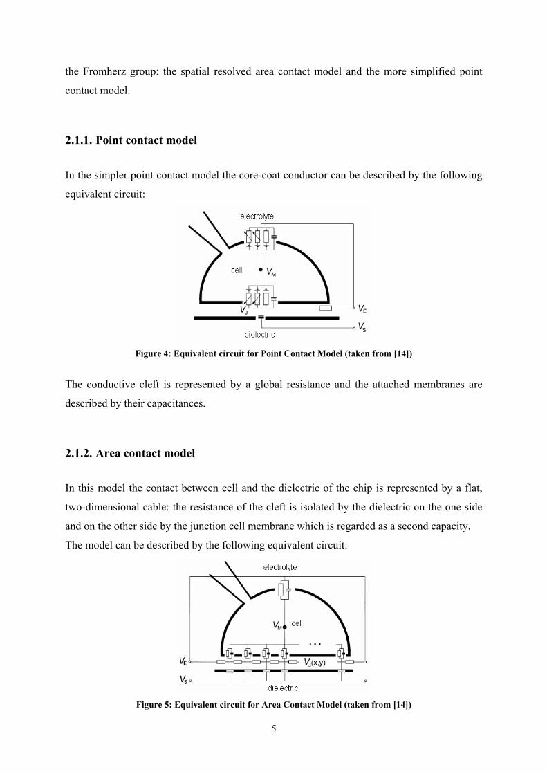
2.1.1. Point contact model
In the simpler point contact model the core-coat conductor can be described by the following
equivalent circuit:
Figure 4: Equivalent circuit for Point Contact Model (taken from [14])
The conductive cleft is represented by a global resistance and the attached membranes are
described by their capacitances.
2.1.2. Area contact model
In this model the contact between cell and the dielectric of the chip is represented by a flat,
two-dimensional cable: the resistance of the cleft is isolated by the dielectric on the one side
and on the other side by the junction cell membrane which is regarded as a second capacity.
The model can be described by the following equivalent circuit:
Figure 5: Equivalent circuit for Area Contact Model (taken from [14])
5
As can be seen in Figure 5 the current is described in each area element by infinitesimal
elements of oxide, membrane and electrolyte which are represented as capacitors and Ohmic
resistances.
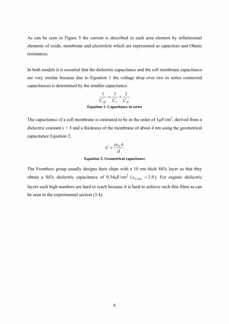
In both models it is essential that the dielectric capacitance and the cell membrane capacitance
are very similar because due to Equation 1 the voltage drop over two in series connected
capacitances is determined by the smaller capacitance.
MSeff CCC111
+=
Equation 1: Capacitance in series
The capacitance of a cell membrane is estimated to be in the order of 1µF/cm2, derived from a
dielectric constant ε = 5 and a thickness of the membrane of about 4 nm using the geometrical
capacitance Equation 2.
dA
C 0εε=
Equation 2: Geometrical capacitance The Fromherz group usually designs their chips with a 10 nm thick SiO2 layer so that they
obtain a SiO2 dielectric capacitance of 0.34µF/cm2 ( 9.32,0 =SiOε ). For organic dielectric
layers such high numbers are hard to reach because it is hard to achieve such thin films as can
be seen in the experimental section (3.4).
6
7
2.2. Signaling in Biology
The communication between cells is mainly done by the exchange of molecules. This can
happen by messaging molecules like cAMP. cGMP, IP3 (2nd messenger) or by ion flux, which
activate all kinds of processes inside a cell and are also responsible for nerve impulse
transport.
As this thesis is aiming for a possible interface between organic materials based information
technology and biology, messaging will be done by ion flux, not with 2nd messengers. To
explain how signalling works in cells we start from the beginning.
2.2.1. The Cell The cell is the structural and functional unit of all living organisms [15], and is sometimes
called the "building block of life." Small organisms like bacteria, consist just of a single cell
whereas other organisms, such as humans have an estimated 100 trillion or 1014 cells. The
size of cells varies from a 2µm up to 200µm.
In large organisms the cells have specified to certain responsibilities, like neurons, skin cells
or sperm cells. Despite this high specialisation there are some features common to all cells:
[16]
• Cell organelles are contained within a cell surface membrane.
• Reproduction by cell division.
• Cells can take up raw material, build cell components, convert energy and molecules
and release the by-products. The functioning of a cell depends upon its ability to
extract and use chemical energy stored in organic molecules.
• Respond to external and internal stimulus, like pH or temperature change.
• Decoding of DNA genes and production of proteins and enzymes.
Derived from the Latin word cellula, a small room, the cell contains all necessary organelles
inside a hull, the plasma membrane (Figure 6).

Figure 6: The Cell (taken from [17])
(1) Nucleolus, (2) Nucleus, (3) Ribosome, (4) Vesicle, (5) rough Endoplasmic Reticulum (ER), (6) Golgi
apparatus, (7) Cytoskeleton, (8) smooth ER, (9) Mitochondrion, (10) Vacuole, (11) Cytoplasm, (12) Lysosome,
(13) Centriole
2.2.2. The plasma membrane As seen above, a living cell is a collection of organelles which are enclosed in a hull, the so-
called plasma membrane. The Plasma membrane has a barrier function, that means it has to
keep all the organelles inside the cell and it has to prevent other molecules from entering the
inside of the cell. Beside this barrier function the membrane must also be permeable for
nutrients and waste for which the membrane is interspersed with channels and pumps.
The basic structure of the Plasma membrane consists of a bilayer of phospholipids (Figure 7)
which have a hydrophilic head group and a hydrophobic tail. In aqueous media they form a
bilayer where the hydrophobic tails face themselves and the hydrophilic head groups face the
media.
Figure 7: Lipid bilayer membrane (taken from [18])
8
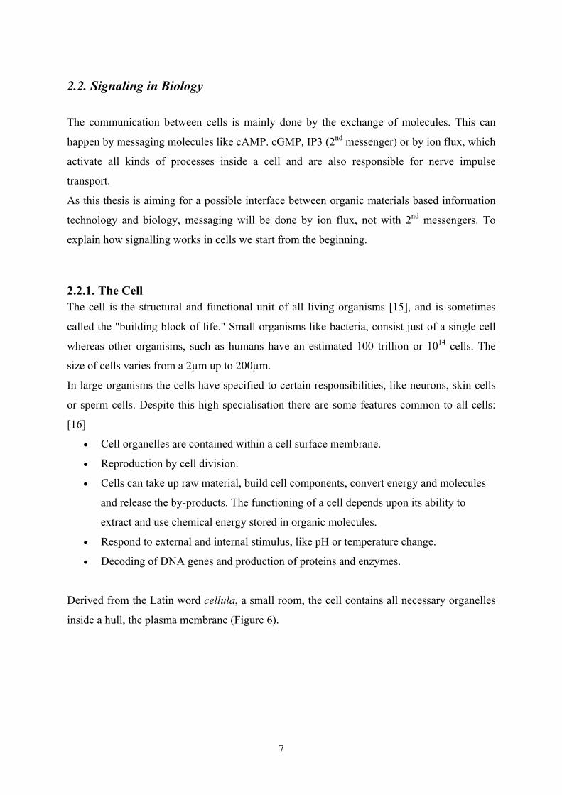
The four major classes of phospholipids for structural use are phosphatidylcholine (PC),
phosphatidylethanolamine (PE), phosphatidylserine (PS) and sphingomyelin (SPHM) (Figure
8).
Figure 8: Phospholipids PC, PE, PS, SPHM
The extra cellular side of the membrane has additionally glycolipids (glucose or
oligosaccharides are covalently bound to lipids) which then form an asymmetrical bilayer and
a protective cover the so-called glycocalix (cell coat). This coat protects the cell and also
mediates the adherence of cells to various surfaces.
One of the essential parts of the cell membrane is the barrier function where the hydrophobic
middle part of the bilayer plays an important role. Small and hydrophobic molecules like O2
or CO2 are just diffusion limited, whereas big molecules are space limited and charged
molecules and ions (K+, Ca2+, Na+, Cl-) are not allowed to pass because of their charge. Being
impermeable for a lot of important messaging molecules and nutrition the cells have
developed specialized proteins which help to transport these molecules and ions.
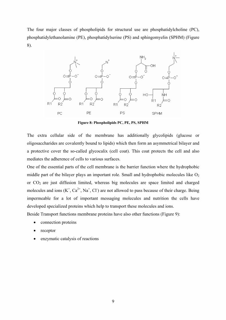
Beside Transport functions membrane proteins have also other functions (Figure 9):
• connection proteins
• receptor
• enzymatic catalysis of reactions
9
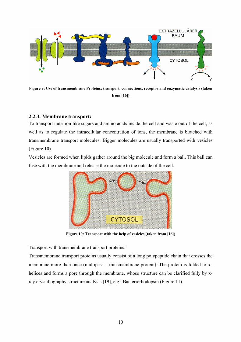
Figure 9: Use of transmembrane Proteins: transport, connections, receptor and enzymatic catalysis (taken
from [16])
2.2.3. Membrane transport: To transport nutrition like sugars and amino acids inside the cell and waste out of the cell, as
well as to regulate the intracellular concentration of ions, the membrane is blotched with
transmembrane transport molecules. Bigger molecules are usually transported with vesicles
(Figure 10).
Vesicles are formed when lipids gather around the big molecule and form a ball. This ball can
fuse with the membrane and release the molecule to the outside of the cell.
Figure 10: Transport with the help of vesicles (taken from [16])
Transport with transmembrane transport proteins:
Transmembrane transport proteins usually consist of a long polypeptide chain that crosses the
membrane more than once (multipass – transmembrane protein). The protein is folded to α-
helices and forms a pore through the membrane, whose structure can be clarified fully by x-
ray crystallography structure analysis [19], e.g.: Bacteriorhodopsin (Figure 11)
10
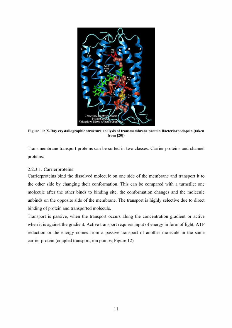
Figure 11: X-Ray crystallographic structure analysis of transmembrane protein Bacteriorhodopsin (taken
from [20])
Transmembrane transport proteins can be sorted in two classes: Carrier proteins and channel
proteins:
2.2.3.1. Carrierproteins: Carrierproteins bind the dissolved molecule on one side of the membrane and transport it to
the other side by changing their conformation. This can be compared with a turnstile: one
molecule after the other binds to binding site, the conformation changes and the molecule
unbinds on the opposite side of the membrane. The transport is highly selective due to direct
binding of protein and transported molecule.
Transport is passive, when the transport occurs along the concentration gradient or active
when it is against the gradient. Active transport requires input of energy in form of light, ATP
reduction or the energy comes from a passive transport of another molecule in the same
carrier protein (coupled transport, ion pumps, Figure 12)
11

Figure 12: Possibilities for transmembrane transport (taken from [21])
2.2.3.2. Ion Channels Ion channels are water filled pores build by one or more membrane proteins (so-called sub
units α, β, γ and so on) through the membrane, which are ion selective (Cl-, Na+, Ca2+ and K+
channels are known) and most important not open all the time, but regulated by different
mechanism [22,23].
Usually the α subunit has most of the functional properties whereas the other subunits control
the structure and activity of the α subunit. Within the α subunit a unit of 300 - 400 amino
acids is repeated 4 times, each repeated unit contains 6 transmembrane domains and each of
the 4 repeated units has a gating mechanism (not necessarily a voltage gated as seen in Figure
13, the yellow transmembrane tube). The four repeat units are arranged circular to form the
water filled pore (Figure 15).
12
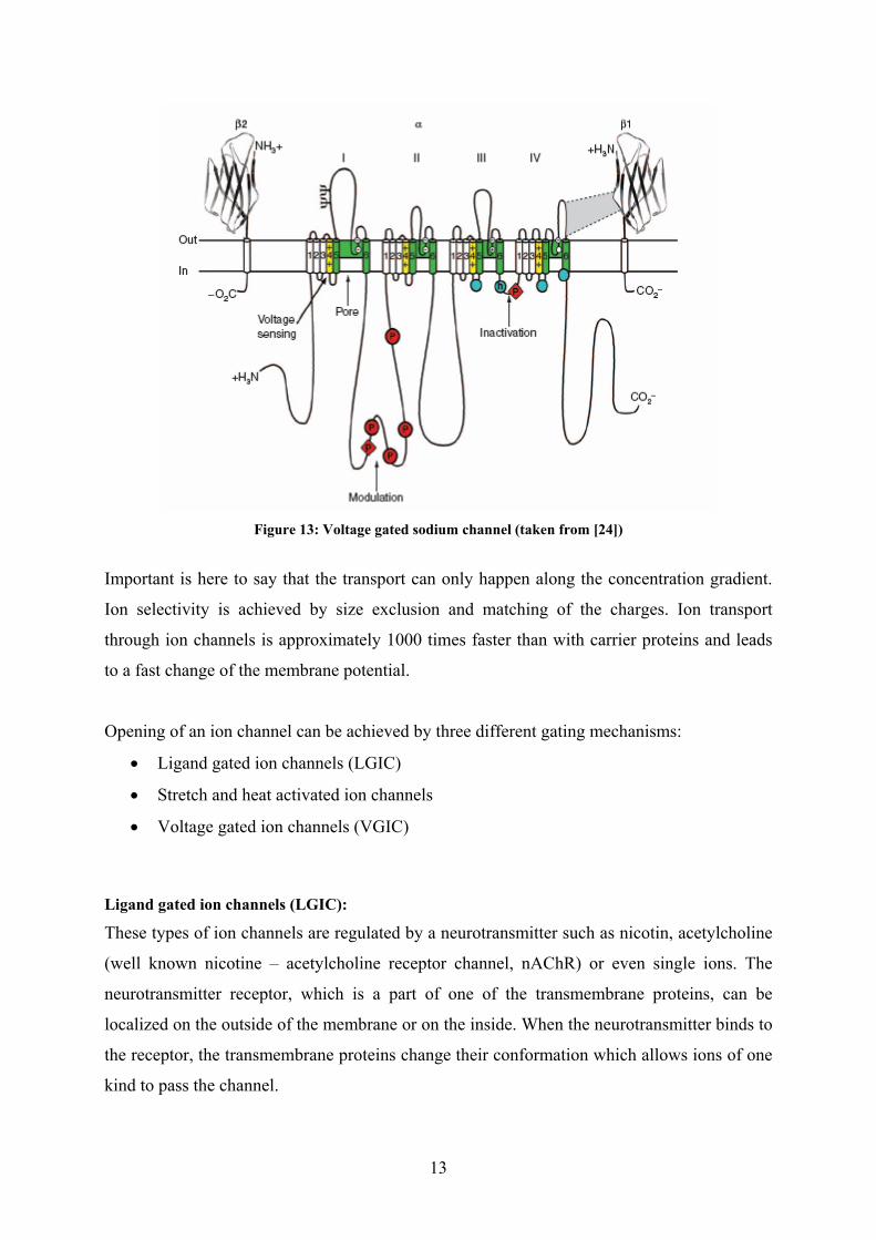
Figure 13: Voltage gated sodium channel (taken from [24])
Important is here to say that the transport can only happen along the concentration gradient.
Ion selectivity is achieved by size exclusion and matching of the charges. Ion transport
through ion channels is approximately 1000 times faster than with carrier proteins and leads
to a fast change of the membrane potential.
Opening of an ion channel can be achieved by three different gating mechanisms:
• Ligand gated ion channels (LGIC)
• Stretch and heat activated ion channels
• Voltage gated ion channels (VGIC)
Ligand gated ion channels (LGIC):
These types of ion channels are regulated by a neurotransmitter such as nicotin, acetylcholine
(well known nicotine – acetylcholine receptor channel, nAChR) or even single ions. The
neurotransmitter receptor, which is a part of one of the transmembrane proteins, can be
localized on the outside of the membrane or on the inside. When the neurotransmitter binds to
the receptor, the transmembrane proteins change their conformation which allows ions of one
kind to pass the channel.
13
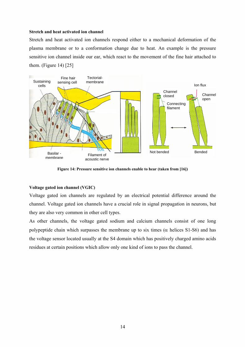
Stretch and heat activated ion channel
Stretch and heat activated ion channels respond either to a mechanical deformation of the
plasma membrane or to a conformation change due to heat. An example is the pressure
sensitive ion channel inside our ear, which react to the movement of the fine hair attached to
them. (Figure 14) [25]
Basilar -membrane
Fine hair sensing cells
Tectorial- membrane
Filament of acoustic nerve
Not bended
Connecting filament
Channel closed
Ion flux
Bended
Sustaining cells
Channel open
Figure 14: Pressure sensitive ion channels enable to hear (taken from [16])
Voltage gated ion channel (VGIC)
Voltage gated ion channels are regulated by an electrical potential difference around the
channel. Voltage gated ion channels have a crucial role in signal propagation in neurons, but
they are also very common in other cell types.
As other channels, the voltage gated sodium and calcium channels consist of one long
polypeptide chain which surpasses the membrane up to six times (α helices S1-S6) and has
the voltage sensor located usually at the S4 domain which has positively charged amino acids
residues at certain positions which allow only one kind of ions to pass the channel.
14
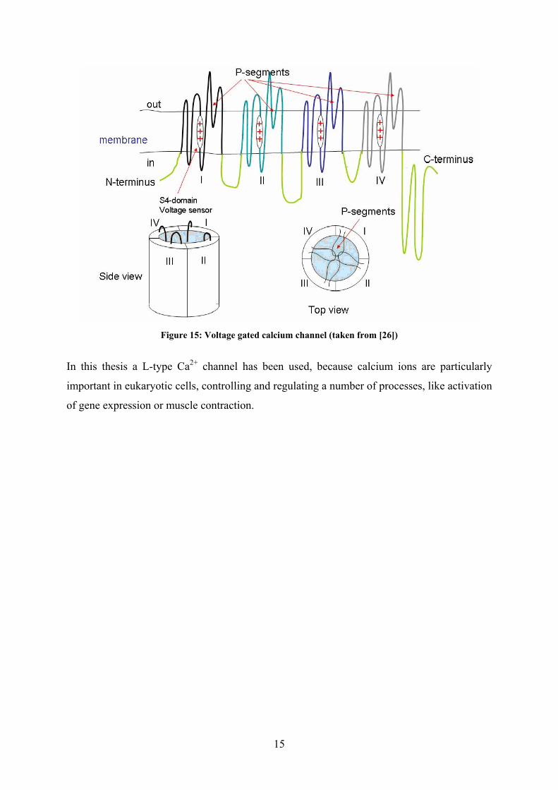
Figure 15: Voltage gated calcium channel (taken from [26])
In this thesis a L-type Ca2+ channel has been used, because calcium ions are particularly
important in eukaryotic cells, controlling and regulating a number of processes, like activation
of gene expression or muscle contraction.
15
2.3. Signaling in Information Technology
As mentioned before, this thesis wants to show the possibility of an interface between organic
materials based information technology devices and cells. Therefore the basic
electrical/electronical devices which maybe used for this kind of interfaces are: a capacitor
and a transistor
2.3.1. The (organic) capacitor
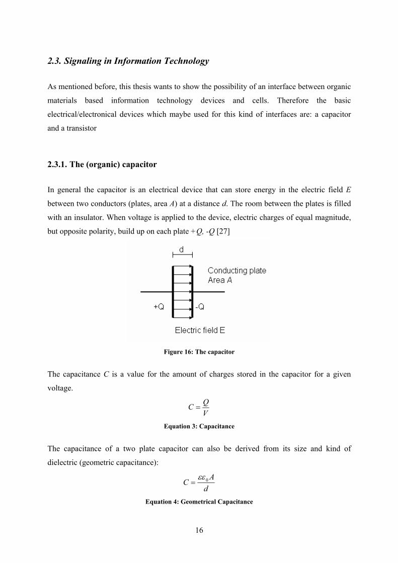
In general the capacitor is an electrical device that can store energy in the electric field E
between two conductors (plates, area A) at a distance d. The room between the plates is filled
with an insulator. When voltage is applied to the device, electric charges of equal magnitude,
but opposite polarity, build up on each plate +Q, -Q [27]
Figure 16: The capacitor
The capacitance C is a value for the amount of charges stored in the capacitor for a given
voltage.
VQC =
Equation 3: Capacitance
The capacitance of a two plate capacitor can also be derived from its size and kind of
dielectric (geometric capacitance):
dA
C 0εε=
Equation 4: Geometrical Capacitance
16
Where ε is the permittivity of the dielectric between the two metal plates and ε0 is the vacuum
permittivity (ε0 = 8.8541878176 × 10⁻¹² F/m), d is the thickness and A the area of the
capacitor. Values for ε in organic materials are typical in the order of 1to 10 (e.g. PVA ~ 8).
To achieve high capacitance per unit area one can either vary the material itself and therefore
have different permittivity constants or change the thickness of the materials. As the
permittivity constants of organic dielectrics are in the same range and even higher than that of
SiO2 the thickness of the organic dielectric will be a crucial part to obtain high capacitance
per unit area values which can be used in a cell – chip junction.
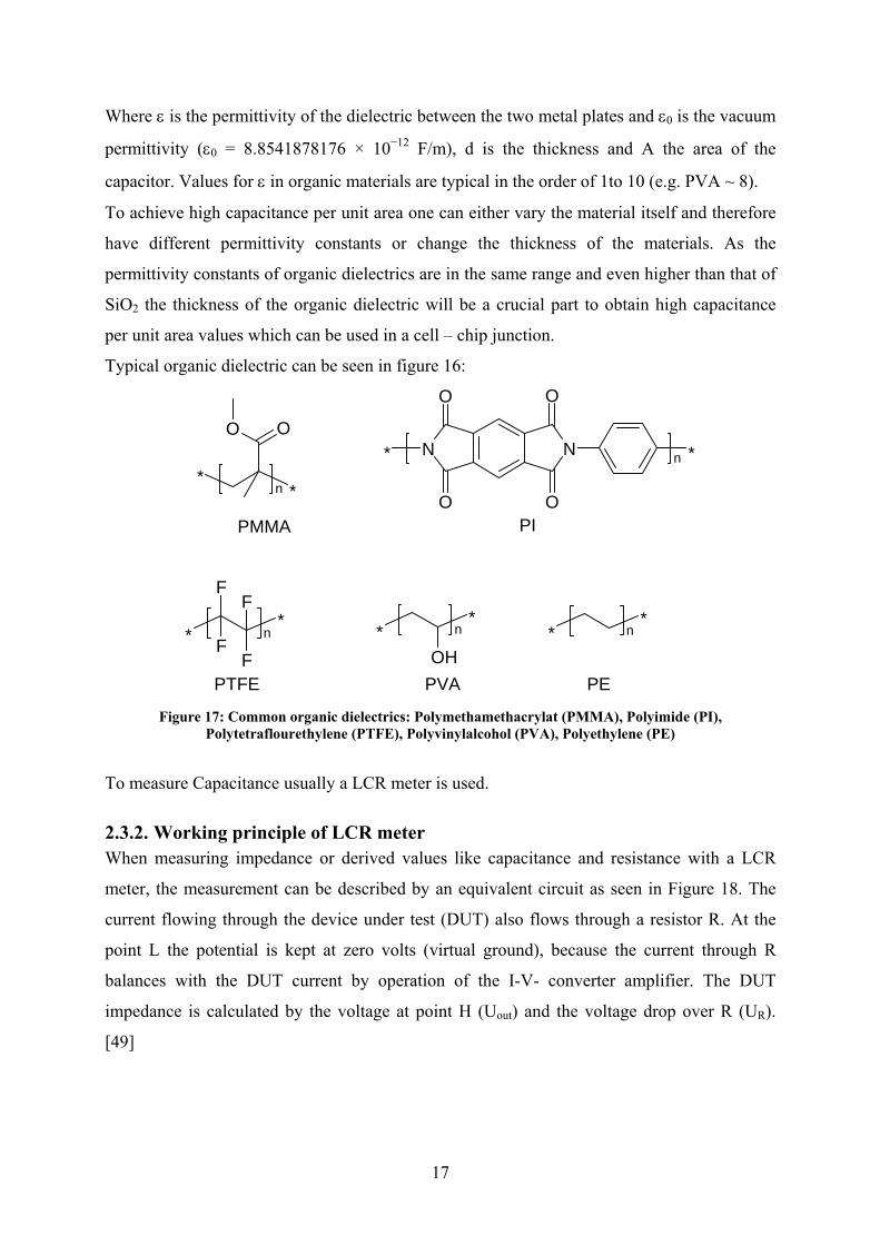
Typical organic dielectric can be seen in figure 16:
**
OO
n
N N
O O
OO
** n
**
F
F
F
F
n
**
OHn
**
n
PMMA PI
PTFE PVA PE Figure 17: Common organic dielectrics: Polymethamethacrylat (PMMA), Polyimide (PI),
Polytetraflourethylene (PTFE), Polyvinylalcohol (PVA), Polyethylene (PE)
To measure Capacitance usually a LCR meter is used.
2.3.2. Working principle of LCR meter When measuring impedance or derived values like capacitance and resistance with a LCR
meter, the measurement can be described by an equivalent circuit as seen in Figure 18. The
current flowing through the device under test (DUT) also flows through a resistor R. At the
point L the potential is kept at zero volts (virtual ground), because the current through R
balances with the DUT current by operation of the I-V- converter amplifier. The DUT
impedance is calculated by the voltage at point H (Uout) and the voltage drop over R (UR).
[49]
17
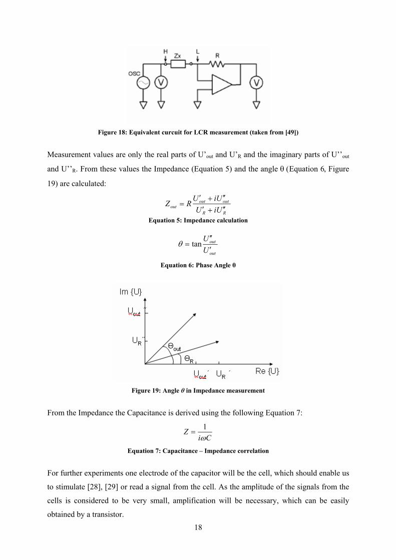
Figure 18: Equivalent curcuit for LCR measurement (taken from [49])
Measurement values are only the real parts of U’out and U’R and the imaginary parts of U’’out
and U’’R. From these values the Impedance (Equation 5) and the angle θ (Equation 6, Figure
19) are calculated:
RR
outoutout UiU
UiURZ
′′+′′′+′
=
Equation 5: Impedance calculation
out
out
UU
′′′
= tanθ
Equation 6: Phase Angle θ
Figure 19: Angle θ in Impedance measurement
From the Impedance the Capacitance is derived using the following Equation 7:
CiZ
ω1
=
Equation 7: Capacitance – Impedance correlation
For further experiments one electrode of the capacitor will be the cell, which should enable us
to stimulate [28], [29] or read a signal from the cell. As the amplitude of the signals from the
cells is considered to be very small, amplification will be necessary, which can be easily
obtained by a transistor. 18

Before explaining the organic field-effect transistor one should explain how organic polymers
can be semi-conducting.
2.3.3. Organic Semiconductors Semiconductors in general are compounds whose conducting properties are somewhere
between those of a metal and an insulator. The conductivity and other electrical properties of
semiconductors are determined by the material's electronic band structure. These electrical
properties may be modified by introducing impurities in a process known as doping. Till the
already mentioned discovery of organic semi conducting polymers by H. Shirakawa, A.G.
MacDiarmid and A.J. Heeger in 1977, this property was attributed to inorganic materials like
Germanium and Silicon.
The materials can be doped in various ways (Figure 20):
Figure 20: Doping mechanism and related applications (taken from [13])
As can be seen in Figure 20 interfacial doping of conjugated polymers is a way to obtain
organic field-effect transistors, which means that electrons and holes are injected from
metallic contacts into the π* – and π – bands (LUMO & HOMO), respectively:
• Hole injection into a already filled π – band:
(π – polymer)n – y(e-) => (π – polymer)n+y
• Electron injection into an empty π* – band:
(π – polymer)n + y(e-) => (π – polymer)n-y
19
Hole and electron injection at the metal semiconductor interface leads to oxidation or
reduction of the polymer but the polymer is not doped in the sense of chemical or
electrochemical doping because there are no counter ions present. [13]
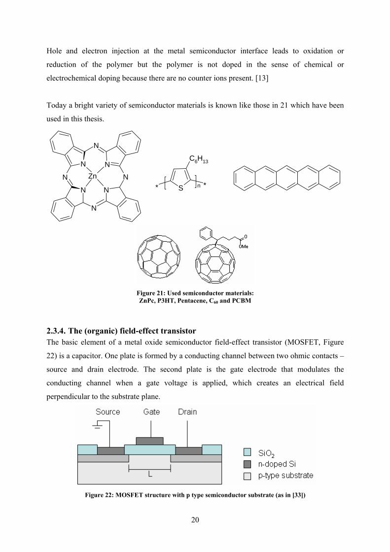
Today a bright variety of semiconductor materials is known like those in 21 which have been
used in this thesis.
NZn
N
N
N
N
N
N
N
S
C6H13
* *n
Figure 21: Used semiconductor materials: ZnPc, P3HT, Pentacene, C60 and PCBM
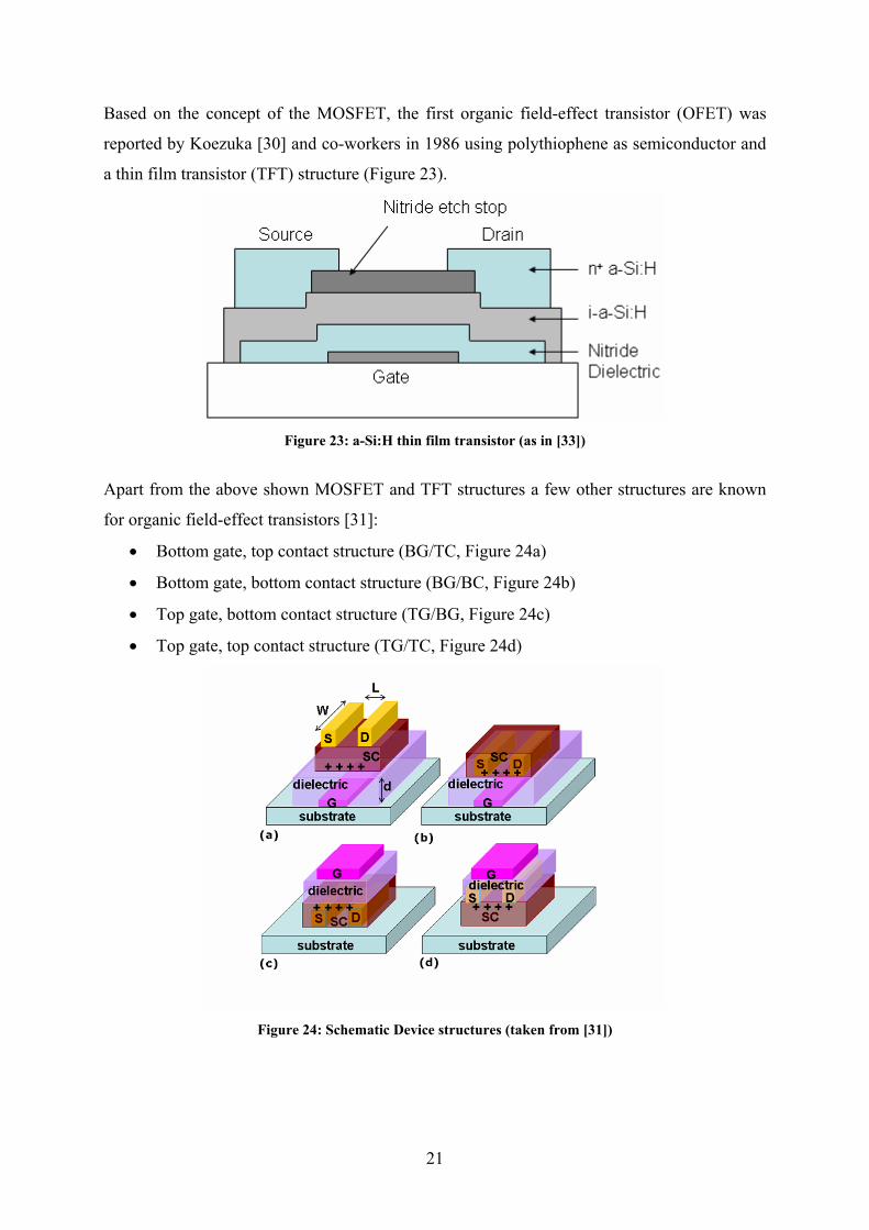
2.3.4. The (organic) field-effect transistor The basic element of a metal oxide semiconductor field-effect transistor (MOSFET, Figure
22) is a capacitor. One plate is formed by a conducting channel between two ohmic contacts –
source and drain electrode. The second plate is the gate electrode that modulates the
conducting channel when a gate voltage is applied, which creates an electrical field
perpendicular to the substrate plane.
Figure 22: MOSFET structure with p type semiconductor substrate (as in [33])
20
Based on the concept of the MOSFET, the first organic field-effect transistor (OFET) was
reported by Koezuka [30] and co-workers in 1986 using polythiophene as semiconductor and
a thin film transistor (TFT) structure (Figure 23).
Figure 23: a-Si:H thin film transistor (as in [33])
Apart from the above shown MOSFET and TFT structures a few other structures are known
for organic field-effect transistors [31]:
• Bottom gate, top contact structure (BG/TC, Figure 24a)
• Bottom gate, bottom contact structure (BG/BC, Figure 24b)
• Top gate, bottom contact structure (TG/BG, Figure 24c)
• Top gate, top contact structure (TG/TC, Figure 24d)
Figure 24: Schematic Device structures (taken from [31])
21
For applications with cells, the metal gate of the top gate transistor will be replaced by the cell
culture as it has been shown already by the Fromherz group on Si-based field-effect
transistors [32].
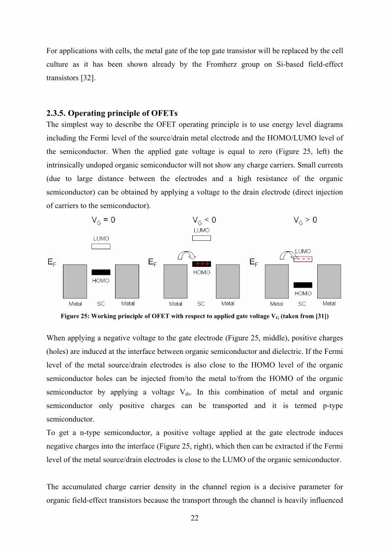
2.3.5. Operating principle of OFETs The simplest way to describe the OFET operating principle is to use energy level diagrams
including the Fermi level of the source/drain metal electrode and the HOMO/LUMO level of
the semiconductor. When the applied gate voltage is equal to zero (Figure 25, left) the
intrinsically undoped organic semiconductor will not show any charge carriers. Small currents
(due to large distance between the electrodes and a high resistance of the organic
semiconductor) can be obtained by applying a voltage to the drain electrode (direct injection
of carriers to the semiconductor).
Figure 25: Working principle of OFET with respect to applied gate voltage VG (taken from [31])
When applying a negative voltage to the gate electrode (Figure 25, middle), positive charges
(holes) are induced at the interface between organic semiconductor and dielectric. If the Fermi
level of the metal source/drain electrodes is also close to the HOMO level of the organic
semiconductor holes can be injected from/to the metal to/from the HOMO of the organic
semiconductor by applying a voltage Vds. In this combination of metal and organic
semiconductor only positive charges can be transported and it is termed p-type
semiconductor.
To get a n-type semiconductor, a positive voltage applied at the gate electrode induces
negative charges into the interface (Figure 25, right), which then can be extracted if the Fermi
level of the metal source/drain electrodes is close to the LUMO of the organic semiconductor.
The accumulated charge carrier density in the channel region is a decisive parameter for
organic field-effect transistors because the transport through the channel is heavily influenced
22
23
by the interface of the organic dielectric and the semiconductor. The basic device parameters
for modelling of organic field-effect transistors are the properties of the insulating layer, the
channel length L, which is the distance between the two metal electrodes and the thickness of
the semi conducting layer W (Figure 24).
24
3. Experimental
3.1. Compatibility test
Before any cell-chip devices can be build one has to ensure that the cell actually likes to
adhere on the surface. To test the cell compatibility all materials were spin coated or vacuum
deposited on 30 mm diameter untreated, cleaned glass cover slides.
3.1.1. Sample Preparation To ensure best adherence of dielectric or semiconductor materials the 30 mm glass cover
slides were in a first step cleaned in a 2 % solution of “Hellmanex” (purchased from Hellma
GmbH) in water in the ultrasonic bath. After 15 minutes or longer the cover slides were
washed with de-ionized water, ethanol and again with water. The ethanol washing step was
inserted to ensure that the cover slide is free of any living materials like bacteria and fungi, to
make sure the applied cell culture is not contaminated.
Spin coating was done with the standard spin coating program used in our laboratory: the
sample holder was accelerated within 4 seconds to 1500 rounds per minute kept at this speed
for 40 seconds and further accelerated to 2000 rpm and held there for 20 seconds before
slowing down. Spin Coating was either done inside the argon glove box (MBraun) for air
sensitive materials or outside the glove box for all other materials.
Evaporation of small molecule semiconductor was done in our laboratory’s Leybold
UNIVEX multi source evaporation machine.
3.1.2. Sterilization All samples were kept inside in a sterile laminar flow-box under UV irradiation over night to
ensure a sterile surface before the cells were seeded.
3.1.3. HEK293 cell line Human Embryonic Kidney Cells are adhering fibroblast-like cells, growing mostly in
monolayer, which have their origin in primary kidney tissue that was transformed with
Adenovirus AD5 by F. Graham and co-workers at McMaster University in 1977. [34]
HEK293 cells have a doubling time of 20 to 24 hours and are kept in a medium containing 90
% Dulbecco’s Modified Eagle Medium (DMEM), 10 % Fetal calf serum (FCS) and some
antibiotics (for Ingredients of DMEM see 8.1Appendix A). The HEK293 cell line is well
established and well characterized throughout the scientific community.
Usually this type of cells adheres within the first five hours to the surface. After this they
continue to reproduce themselves. In case of not adhering to the surface the cells cluster to big
clouds of cells, so that they feel like adhering and start reproducing.
3.1.4. Cell culturing Cells were cultured in DMEM in an incubator at 37 °C and 98 % humidity in air, containing 5
% CO2 over night before the result of the cell culturing was checked by light microscopy on
the next day.
3.1.5. Tested materials The following dielectric and semiconductor materials have been investigated if they are
compatible with the HEK293 cell line.
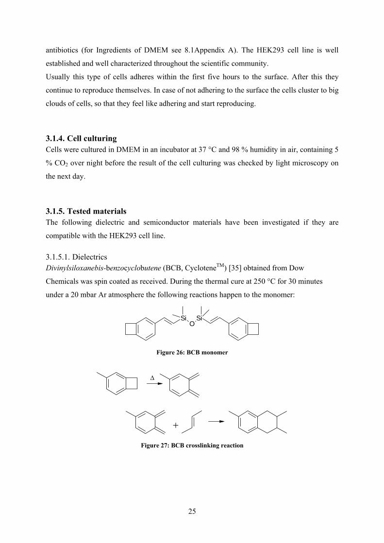
3.1.5.1. Dielectrics Divinylsiloxanebis-benzocyclobutene (BCB, CycloteneTM) [35] obtained from Dow
Chemicals was spin coated as received. During the thermal cure at 250 °C for 30 minutes
under a 20 mbar Ar atmosphere the following reactions happen to the monomer:
OSiSi
Figure 26: BCB monomer
Δ
+
Figure 27: BCB crosslinking reaction
25

OSiSiSi
Si
n
Figure 28: Thermally cross linked BCB
Polyimide (KemititeTM CT4112, PI) was obtained from Kyocera Chemicals Corp. and used as
received (Polyimide precursor polyamic acid in N-methylpyrolidon) [36]. The spin coated
films were first heated to 75 °C for 30 minutes to avoid strong shrinking of the film, before
heating to 180 °C for one hour.
RO
O
NHOH
R
O
O
OHNH R
N
O
O
RR
NR
O
O
*
n
Polyamic acid
Polyimide
T
Figure 29: Thermally cured polyimide
Since Polyvinylphenol (PVP) is water soluble and can therefore not be used as a surface for
cells, the PVP was crosslinked with methylated poly (melamine-co-formaldehyde) [37]. As a
solvent 1, 2-Propanediol monomethyl ether acetate (PMA) was used. The spin coated film
was annealed at 190 °C for 30 minutes.
26
N
N
NN N
N
O O
O O
O*
* ***
n
O*
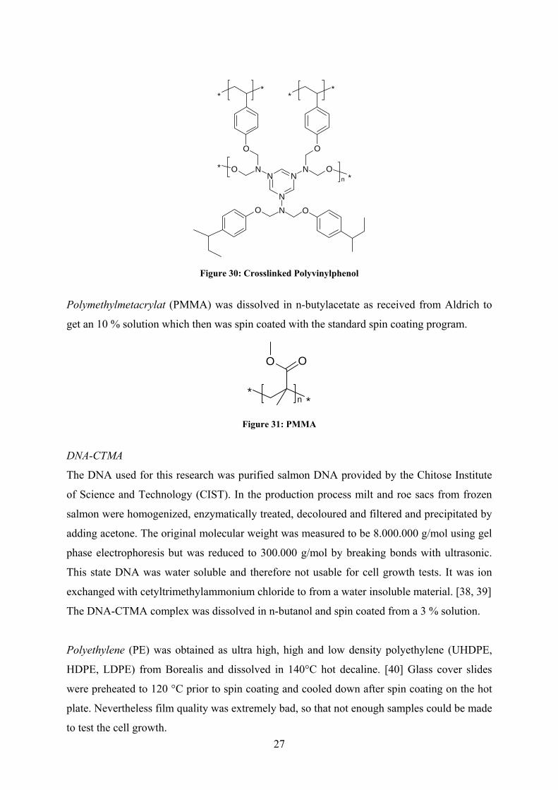
Figure 30: Crosslinked Polyvinylphenol
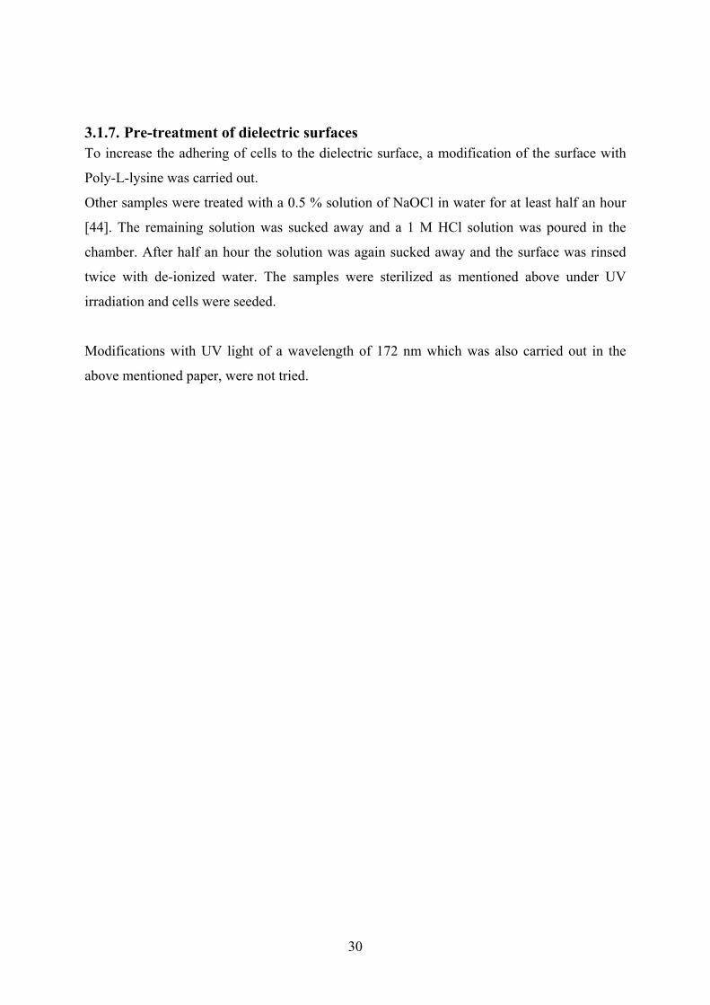
Polymethylmetacrylat (PMMA) was dissolved in n-butylacetate as received from Aldrich to
get an 10 % solution which then was spin coated with the standard spin coating program.
**
OO
n
Figure 31: PMMA
DNA-CTMA
The DNA used for this research was purified salmon DNA provided by the Chitose Institute
of Science and Technology (CIST). In the production process milt and roe sacs from frozen
salmon were homogenized, enzymatically treated, decoloured and filtered and precipitated by
adding acetone. The original molecular weight was measured to be 8.000.000 g/mol using gel
phase electrophoresis but was reduced to 300.000 g/mol by breaking bonds with ultrasonic.
This state DNA was water soluble and therefore not usable for cell growth tests. It was ion
exchanged with cetyltrimethylammonium chloride to from a water insoluble material. [38, 39]
The DNA-CTMA complex was dissolved in n-butanol and spin coated from a 3 % solution.
Polyethylene (PE) was obtained as ultra high, high and low density polyethylene (UHDPE,
HDPE, LDPE) from Borealis and dissolved in 140°C hot decaline. [40] Glass cover slides
were preheated to 120 °C prior to spin coating and cooled down after spin coating on the hot
plate. Nevertheless film quality was extremely bad, so that not enough samples could be made
to test the cell growth. 27

Cyanoethylpullulan (CyEPl) [41] is the converted product of pullulan, a polysaccaridic
polymer which is gained by micro organism. The chemical structure of pullulan depends on
the carbon source, the producing organism (different strains of Aureobasidium pullulans) and
fermentation conditions. Basic structure consist of 3 α-1,4-glycosidic bond glucose molecules
forming the maltotriose unit, which then is α-1,6-glycsidic bond to other units. Up to 10 %
Maltotetrose units and a-1,3-glyocosidic bonds are also possible depending on above
mentioned conditions. [42]
Pullulan is reacted with acrylonitril to get CyEPl, which was obtained from Shin Etsu
Chemical Co. Ltd. The material has a good solubility in various organic solvents, like N-
methylpyrolidon (NMP), which was used in this study to spin coat the CyEPl.
O
OR OR
OR
O *O
OR OR
OR
O
O
OR OR
O
O
OR OR
OR
O
O
OR OR
OR
O
O
OR OR
OR
O*
n
R = CH2-CH2-CN
Figure 32: CyEPl
Polystyrene (PS) was obtained from Aldrich and dissolved in chlorobenzene to get a 10 %
solution, which was then spin coated onto the cover slides.
**
n
Figure 33: Polystyrene
PDMS: Sylgard® 184 Base (Tetra(trimethylsiloxy)silan) and Sylgard® 184 Curing Agent
(Tetramethyltetravinylcyclotetrasiloxane) were obtained from Dow Corning and mixed 1:10
by volume. After spin coating the films were thermally cured at 125 °C for twenty minutes
according to the manufacturer instruction [43]
28

Polyelectrolyte: PEO:LiClO4
Motivated by the extremely large capacitance per unit area (5 µF/cm2) of this material both
Polyethyleneoxide (PEO) and Lithiumperchlorate (LiClO4) were used as obtained from
SigmaAldrich and dissolved in acetonitril to achieve a 16:1 ether oxygen-to-lithium ion
stoichiometric ratio [51].
O*n
Figure 34: Polyethyleneoxide
During the experiments it was discovered that the PEO:LiClO4 film is highly water-soluble
and therefore the cells didn’t grow on the film but onto the glass slide after the film had
dissolved in the aqueous media of the cell culture. Therefore no pictures will be shown in the
results section. (4.1)
3.1.5.2. Semiconductors Regioregular P3HT (Poly-(3-hexylthiophene-2, 5-diyl)) films were prepared by spin coating
from a 3 % in Chlorobenzene solution. P3HT was used as obtained from Riecke Metals
ZnPc (zinc phthalcyanine) was deposited with Leybold UNIVEX350 vacuum evaporation
machine, where the nominal film thickness was set to 100 nm. The material was obtained
from Sigma Aldrich and purified by sublimation prior to use.
100 nm pentacene were also deposited with UNIVEX350 vacuum deposition machine. The
material was used as obtained from Aldrich
C60 was used as obtained from MER Corp. and was also deposited with UNIVEX350 vacuum
deposition machine.
PCBM ([6,6]-phenyl C61-butyric acid methyl ester) is the soluble derivative of C60 and was
spin coated from 20 – µm filtered 3 % Chlorobenzene solution. Material was used as obtained
from Nano-C.
3.1.6. Light microscopy Light microscopy was carried out on inverted microscope fabricated by Nikon (Eclipse
TE200). Digital Imagine was done by a SENSICAM CCD camera. 29
30
3.1.7. Pre-treatment of dielectric surfaces To increase the adhering of cells to the dielectric surface, a modification of the surface with
Poly-L-lysine was carried out.
Other samples were treated with a 0.5 % solution of NaOCl in water for at least half an hour
[44]. The remaining solution was sucked away and a 1 M HCl solution was poured in the
chamber. After half an hour the solution was again sucked away and the surface was rinsed
twice with de-ionized water. The samples were sterilized as mentioned above under UV
irradiation and cells were seeded.
Modifications with UV light of a wavelength of 172 nm which was also carried out in the
above mentioned paper, were not tried.

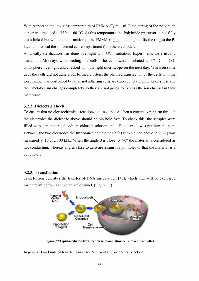
3.2. Activation of ion channels in HEK cells
As stated in the introduction it should be possible to activate ion channels by polarizing the
membrane with a polarized dielectric. To check if this is possible for organic dielectrics the
following experiment was designed (Figure 36).
Cells are seeded above the dielectric covered metal electrodes and after one day of incubation
they are transfected with calcium ion channels. By applying a bias between a bath electrode
and the metal electrode under the dielectric, the dielectric will be polarized, leading to a
polarization of the membrane, which then will open the ion channel. If this is the case,
calcium ions stream into the cell and bind there to the Ca2+ selective fluorescence dye FURA-
2AM (Figure 35, excitation wavelength λ = 340 nm & λ = 380 nm), which can be detected by
fluorescence microscopy.
ON
O
ON
O
OO
NO
OOO
OOOO
5K+
Figure 35: Fura-2AM molecule
31
Pt
PI Cr/Au glass
HEK cells
Electrolyte
Ratio: 340nm/380nm
FG
PMMA
CCD camera
Figure 36: Ion channel activation experiment
3.2.1. Device Preparation After cleaning glass cover slides metal electrodes were vacuum deposited. This was done with
the evaporation unit inside glove box II. Because light microscopy should be carried out in the
further course of the experiment the electrodes were design to be transparent. Therefore a 20
nm gold electrode was evaporated. To ensure adherence of the electrode to the glass surface a
1 nm chromium layer was first applied to the glass. Five samples were prepared with ZnO
doped with Al sputtered onto cover glasses as an electrode.
Afterwards the dielectric was spun onto the slides and again removed from the edges of the
electrodes to be able to contact them later. For this experiment the results of the cell
compatibility test where applied so that only Polyimide was used. After the annealing step of
PI at 180 °C a PMMA ring was glued to the PI-cover slide to contain the cell medium away
from the electrodes. As glue the polyimide precursor was used after preliminary experiments
showed that usual glues transpired remaining solvents into the cell medium leading to death
of the cells.
32
With respect to the low glass temperature of PMMA (Tg = 110°C) the curing of the polyimide
cursor was reduced to 150 – 160 °C. At this temperature the Polyimide precursor is not fully
cross linked but with the deformation of the PMMA ring good enough to fix the ring to the PI
layer and to seal the so formed cell compartment from the electrodes.
As usually sterilization was done overnight with UV irradiation. Experiments were usually
started on Mondays with seeding the cells. The cells were incubated at 37 °C in CO2
atmosphere overnight and checked with the light microscope on the next day. When on some
days the cells did not adhere but formed clusters, the planned transfection of the cells with the
ion channel was postponed because not adhering cells are exposed to a high level of stress and
their metabolism changes completely so they are not going to express the ion channel in their
membrane.
3.2.2. Dielectric check To ensure that no electrochemical reactions will take place when a current is running through
the electrodes the dielectric above should be pin hole free. To check this, the samples were
filled with 1 ml saturated sodium chloride solution and a Pt electrode was put into the bath.
Between the two electrodes the Impedance and the angle θ (as explained above in 2.3.2) was
measured at 10 and 100 kHz. When the angle θ is close to -90° the material is considered as
not conducting, whereas angles close to zero are a sign for pin holes or that the material is a
conductor.
3.2.3. Transfection Transfection describes the transfer of DNA inside a cell [45], which then will be expressed
inside forming for example an ion channel. (Figure 37)
Figure 37:Lipid-mediated transfection in mammalian cells (taken from [46])
In general two kinds of transfection exist: transient and stable transfection.
33
34
By transient transfection is meant that the DNA is not added to the host genome but is extra
chromosomal inside the Plasmid and is transported to the cell core for transcription. Since the
DNA is not in the cell core it is not handed to the next generation.
Stable transfection is meant when the inserted DNA is taken up into the host genome and can
therefore be handed to the next cell generation. Compared to the transient transfection which
can be applied easily for most of the cell lines and different kinds of DNA it takes some time
to get a stable transfected cell line. However when a stable cell line is achieved, one gets
always the same clones, which can be used for a long time until the gene is expelled from the
core again. [47]
In general six different techniques are available:
• Calciumphosphat-Coprecipitation
• Elektroporation
• Lipofection
• Nanofectin™ (PAA)
• Mikroinjection
• DEAE-Dextran-Method
In the course of this thesis transient transfections by Lipofection were carried out. Different
transfection agents were used to check which one will give the highest yield of transfected
cells, which depends on the combination of cell line type and DNA:
• TransfectinTM Lipid Reagent by BIO-RAD
• SuperfectTM by Quiagen
• ExGen500TM by Fermentas
• LipofectaminTM by Invitrogen
The transfection protocols can be found in the Appendix B.
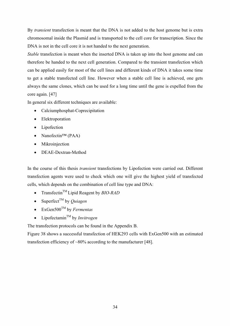
Figure 38 shows a successful transfection of HEK293 cells with ExGen500 with an estimated
transfection efficiency of ~80% according to the manufacturer [48].
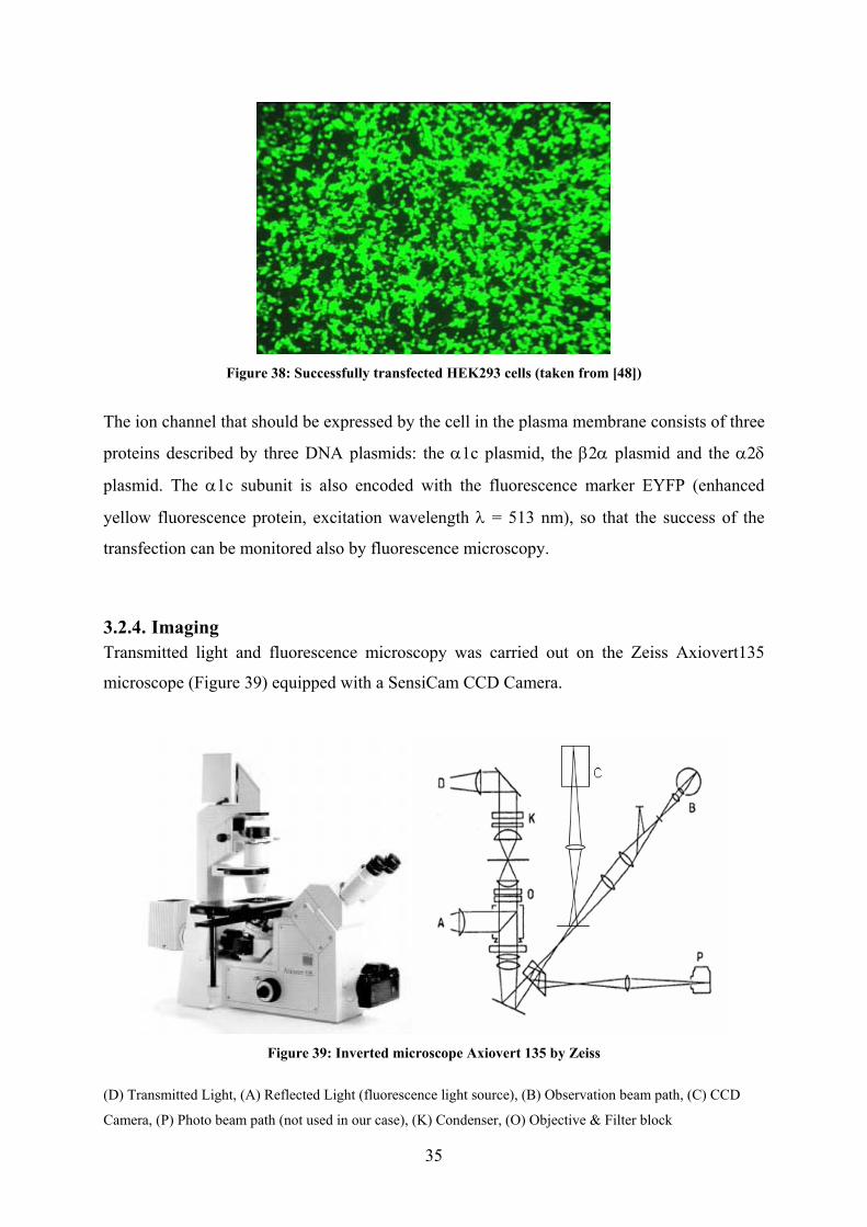
Figure 38: Successfully transfected HEK293 cells (taken from [48])
The ion channel that should be expressed by the cell in the plasma membrane consists of three
proteins described by three DNA plasmids: the α1c plasmid, the β2α plasmid and the α2δ
plasmid. The α1c subunit is also encoded with the fluorescence marker EYFP (enhanced
yellow fluorescence protein, excitation wavelength λ = 513 nm), so that the success of the
transfection can be monitored also by fluorescence microscopy.
3.2.4. Imaging Transmitted light and fluorescence microscopy was carried out on the Zeiss Axiovert135
microscope (Figure 39) equipped with a SensiCam CCD Camera.
Figure 39: Inverted microscope Axiovert 135 by Zeiss
(D) Transmitted Light, (A) Reflected Light (fluorescence light source), (B) Observation beam path, (C) CCD
Camera, (P) Photo beam path (not used in our case), (K) Condenser, (O) Objective & Filter block
35

3.3. Impedance measurements
To see if a tight adhering cell layer changes the capacitance or the impedance of the dielectric
layer impedance measurements were carried out. Since the electrodes cannot be put onto the
cell layer the measurements were carried out with a platinum electrode in the cell medium as
a second electrode (same measurement setup as seen in Figure 36).
The same samples produced for the above mentioned experiment were also used for
Impedance measurements. The frequency dependent impedance was measured using a
HP4284A Precision LCR meter (frequency range: 20 Hz – 1MHz).
3.4. Capacitance Measurement
Capacitance measurements with metal-insulator-metal (MIM) devices were made to compare
the resulting capacitance per unit area with values used in cell – chip junction experiments.
The measurement was carried out with the above mentioned HP4284A Precision LCR meter
(frequency range: 20 Hz – 1MHz).
Figure 40: MIM-Device
Usually the used ITO glass was etched using HClconz and cleaned afterwards with Hellmanex
and rinsed with water. The dielectric was deposited by spin coating and as a second electrode
aluminium was used.
The samples used for the Impedance vs. Frequency measurements were also used to measure
capacitance to check if adhering cells onto the surface have an influence.
36
37
3.5. I-V Measurements
Similar to the Impedance – Frequency measurements for dielectrics, Current – Voltage (I-V)
measurements were carried out for the cells on semiconductor materials. Measurement was
made with the AGILENT E5273A 2 channel source/monitor unit using just one output
channel.
3.6. Top gate transistor
To activate a transistor with a cell as a gate, the operating gate voltage of the transistor has to
be rather low, because the voltage change that can be achieved by the opening of a ion
channel is in the order of some 10 mV. After studying the literature a suitable candidate was
found in a transistor consisting of P3HT as active material and PEO:LiClO4 as a
polyelectrolyte dielectric was used [51]. After discovering that PEO is water-soluble further
experiments to improve the transistor were cancelled.
Employing the results of the cell compatibility tests top gate transistors (Figure 24) with the
suitable dielectrics, were built to show that they are also capable to make good top gate
transistors. Therefore polyimide and cross linked polyvinylphenol were chosen as gate
dielectric.
3.6.1. Device preparation
To get this device 1.5 cm x 1.5 cm glass slides were thoroughly washed with Hellmanex
cleaning solution in the warm ultrasonic bath for at least 15 minutes before rinsing them with
de-ionized water twice and dried with pressurized air.
60 nm aluminum source drain electrodes were evaporated using a shadow mask in the
evaporation machine inside the glove box. Afterwards the samples were transferred to the
UNIVEX350 evaporation machine for C60 evaporation. C60 was chosen as active material
because it is supposed to withstand the elevated temperatures needed to thermally cross link
the Polyimide and Polyvinylphenol precursors.
Usually 200 nm of C60 were evaporated at an average speed of 0.7 Å/sec and a base pressure
of ~5.0 x 10⁻⁶ mbar in the UNIVEX350 evaporation machine.

38
After transferring the samples back into the glove box I, they were spin coated with the
precursor solution with the standard spin coating program: in 4 seconds to 1500 rpm, stay
there for 40, accelerate to 2000 within one second and keep the speed for 20 seconds before
reducing the speed again.
Unfortunately the solvents used in the precursor solution N-methylpyrrolidon (NMP) for
polyimide and Propyleneglycolmonomethyletheracetat (PMA) for cross linked PVP were
very aggressive towards the deposited C60 layer. A drop of NMP strips a 200 nm C60 film of
the glass within a few minutes. During spin coating this effect can also be observed causing
inhomogeneous films, which results in not working devices.
Polyimide samples were cured on the hot plate, first at 75 °C for 30 minutes to avoid strong
shrinking of the film, before heating to 180 °C for one hour as advised by the manufacturer.
Polyvinylphenol samples were thermally annealed at 190 °C for 30 minutes using an oven.
Last but not least 40 nm aluminum were evaporated as gate electrode before testing the
transistor using an AGILENT E5273A 2 channel source/monitor unit.
In another effort, not directly related to the cell-chip junction, a top gate transistor based on
P3HT was build. As a gate dielectric Polyethyleneoxide (PEO) with LiClO4, a solid
electrolyte, was used.
As a substrate 1.5 x 1.5 cm glass slides were used, clean in Hellmanex glass cleaning solution
and rinsed with water. Afterwards P3HT was spin coated from a 3 % solution in
Chlorobenzene with the standard spin coating program inside the glove box.
After the semiconductor layer had dried, 40 nm gold source & drain electrodes were
evaporated. The PEO:LiClO4 electrolyte solution was drop casted outside the glovebox. On
the next day, 40 nm gold were evaporated to form the gate electrode. Measurement was
carried out inside the glove box.
4. Results and Discussion:
4.1. Results of Compatibility test In the following section the results from the compatibility study of cell and
dielectric/semiconductor surface are shown.
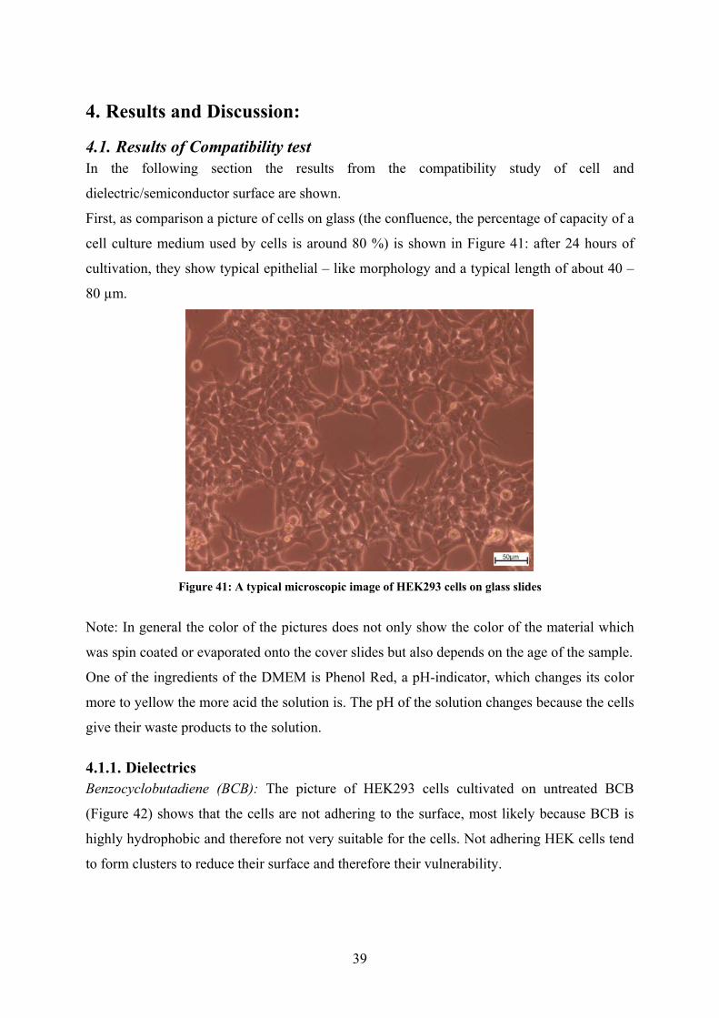
First, as comparison a picture of cells on glass (the confluence, the percentage of capacity of a
cell culture medium used by cells is around 80 %) is shown in Figure 41: after 24 hours of
cultivation, they show typical epithelial – like morphology and a typical length of about 40 –
80 µm.
Figure 41: A typical microscopic image of HEK293 cells on glass slides
Note: In general the color of the pictures does not only show the color of the material which
was spin coated or evaporated onto the cover slides but also depends on the age of the sample.
One of the ingredients of the DMEM is Phenol Red, a pH-indicator, which changes its color
more to yellow the more acid the solution is. The pH of the solution changes because the cells
give their waste products to the solution.
4.1.1. Dielectrics Benzocyclobutadiene (BCB): The picture of HEK293 cells cultivated on untreated BCB
(Figure 42) shows that the cells are not adhering to the surface, most likely because BCB is
highly hydrophobic and therefore not very suitable for the cells. Not adhering HEK cells tend
to form clusters to reduce their surface and therefore their vulnerability.
39
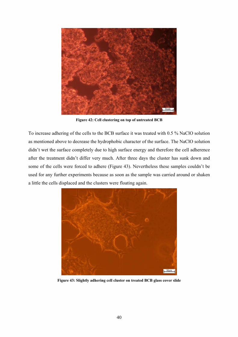
Figure 42: Cell clustering on top of untreated BCB
To increase adhering of the cells to the BCB surface it was treated with 0.5 % NaClO solution
as mentioned above to decrease the hydrophobic character of the surface. The NaClO solution
didn’t wet the surface completely due to high surface energy and therefore the cell adherence
after the treatment didn’t differ very much. After three days the cluster has sunk down and
some of the cells were forced to adhere (Figure 43). Nevertheless these samples couldn’t be
used for any further experiments because as soon as the sample was carried around or shaken
a little the cells displaced and the clusters were floating again.
Figure 43: Slightly adhering cell cluster on treated BCB glass cover slide
40
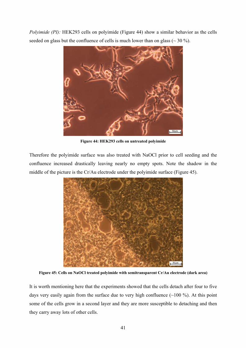
Polyimide (PI): HEK293 cells on polyimide (Figure 44) show a similar behavior as the cells
seeded on glass but the confluence of cells is much lower than on glass (~ 30 %).
Figure 44: HEK293 cells on untreated polyimide
Therefore the polyimide surface was also treated with NaOCl prior to cell seeding and the
confluence increased drastically leaving nearly no empty spots. Note the shadow in the
middle of the picture is the Cr/Au electrode under the polyimide surface (Figure 45).
Figure 45: Cells on NaOCl treated polyimide with semitransparent Cr/Au electrode (dark area)
It is worth mentioning here that the experiments showed that the cells detach after four to five
days very easily again from the surface due to very high confluence (~100 %). At this point
some of the cells grow in a second layer and they are more susceptible to detaching and then
they carry away lots of other cells.
41
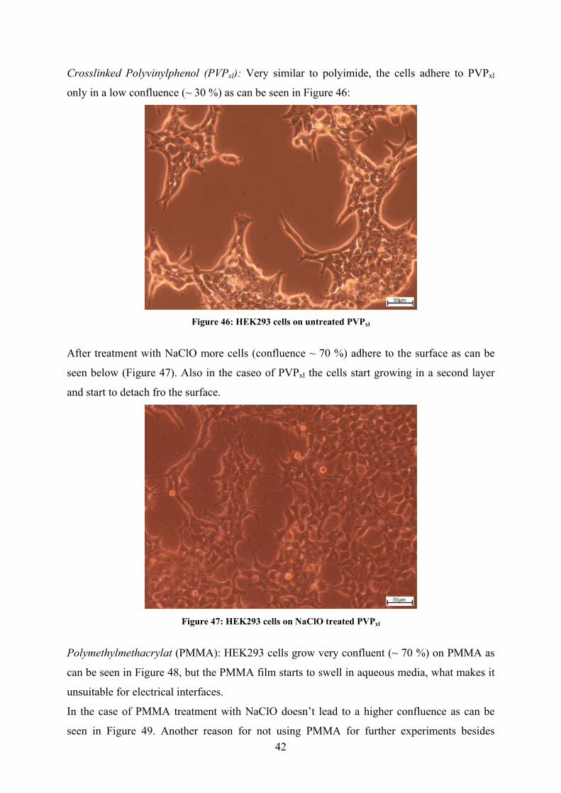
Crosslinked Polyvinylphenol (PVPxl): Very similar to polyimide, the cells adhere to PVPxl
only in a low confluence (~ 30 %) as can be seen in Figure 46:
Figure 46: HEK293 cells on untreated PVPxl
After treatment with NaClO more cells (confluence ~ 70 %) adhere to the surface as can be
seen below (Figure 47). Also in the caseo of PVPxl the cells start growing in a second layer
and start to detach fro the surface.
Figure 47: HEK293 cells on NaClO treated PVPxl
Polymethylmethacrylat (PMMA): HEK293 cells grow very confluent (~ 70 %) on PMMA as
can be seen in Figure 48, but the PMMA film starts to swell in aqueous media, what makes it
unsuitable for electrical interfaces.
In the case of PMMA treatment with NaClO doesn’t lead to a higher confluence as can be
seen in Figure 49. Another reason for not using PMMA for further experiments besides 42
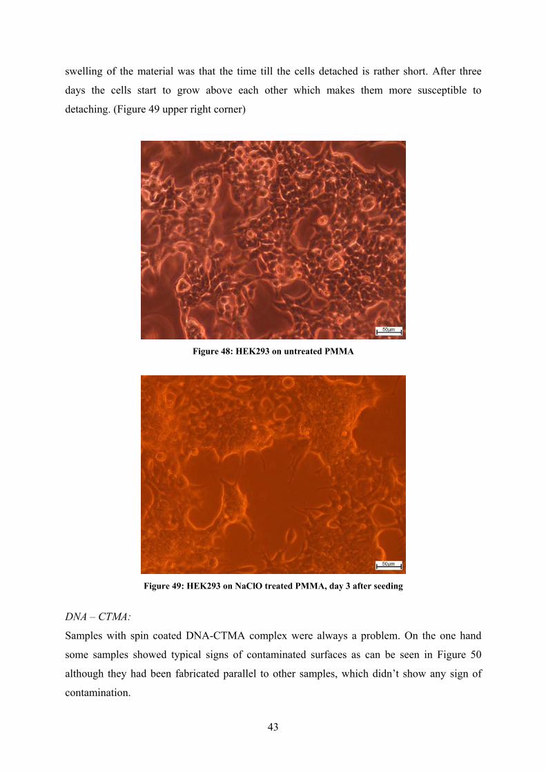
swelling of the material was that the time till the cells detached is rather short. After three
days the cells start to grow above each other which makes them more susceptible to
detaching. (Figure 49 upper right corner)
Figure 48: HEK293 on untreated PMMA
Figure 49: HEK293 on NaClO treated PMMA, day 3 after seeding
DNA – CTMA:
Samples with spin coated DNA-CTMA complex were always a problem. On the one hand
some samples showed typical signs of contaminated surfaces as can be seen in Figure 50
although they had been fabricated parallel to other samples, which didn’t show any sign of
contamination.
43
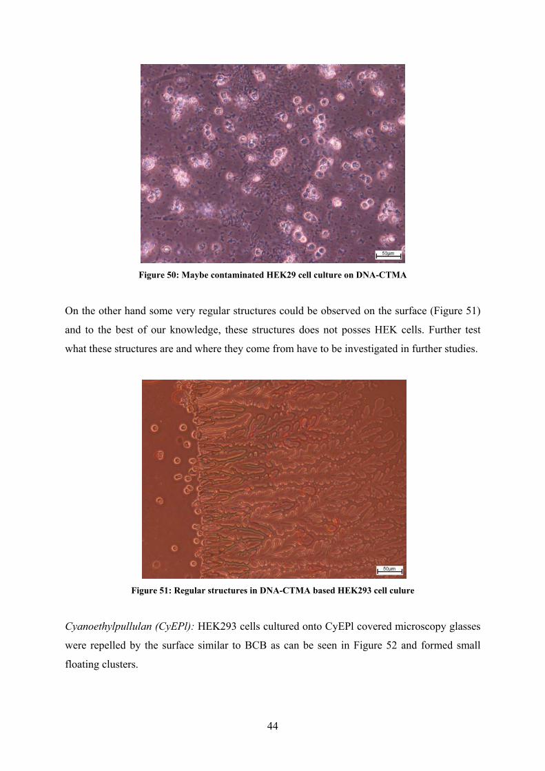
Figure 50: Maybe contaminated HEK29 cell culture on DNA-CTMA
On the other hand some very regular structures could be observed on the surface (Figure 51)
and to the best of our knowledge, these structures does not posses HEK cells. Further test
what these structures are and where they come from have to be investigated in further studies.
Figure 51: Regular structures in DNA-CTMA based HEK293 cell culure
Cyanoethylpullulan (CyEPl): HEK293 cells cultured onto CyEPl covered microscopy glasses
were repelled by the surface similar to BCB as can be seen in Figure 52 and formed small
floating clusters.
44
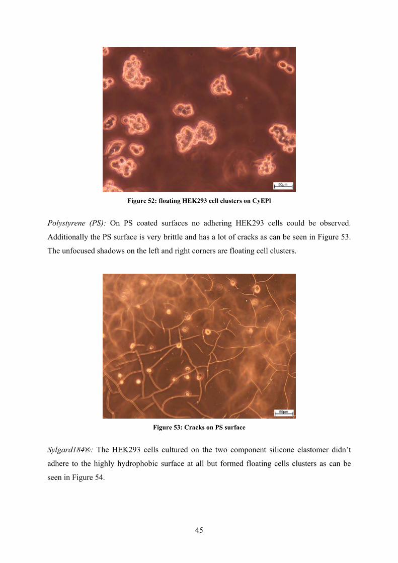
Figure 52: floating HEK293 cell clusters on CyEPl
Polystyrene (PS): On PS coated surfaces no adhering HEK293 cells could be observed.
Additionally the PS surface is very brittle and has a lot of cracks as can be seen in Figure 53.
The unfocused shadows on the left and right corners are floating cell clusters.
Figure 53: Cracks on PS surface
Sylgard184®: The HEK293 cells cultured on the two component silicone elastomer didn’t
adhere to the highly hydrophobic surface at all but formed floating cells clusters as can be
seen in Figure 54.
45
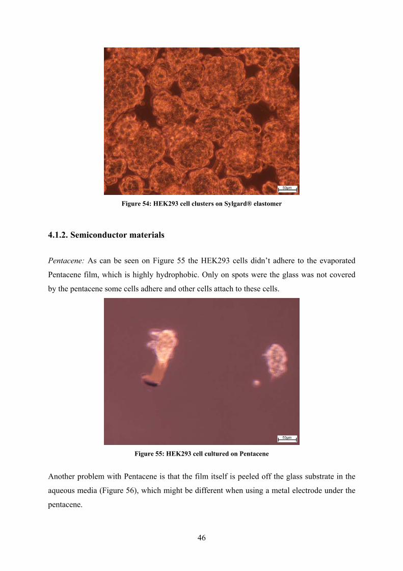
Figure 54: HEK293 cell clusters on Sylgard® elastomer
4.1.2. Semiconductor materials
Pentacene: As can be seen on Figure 55 the HEK293 cells didn’t adhere to the evaporated
Pentacene film, which is highly hydrophobic. Only on spots were the glass was not covered
by the pentacene some cells adhere and other cells attach to these cells.
Figure 55: HEK293 cell cultured on Pentacene
Another problem with Pentacene is that the film itself is peeled off the glass substrate in the
aqueous media (Figure 56), which might be different when using a metal electrode under the
pentacene.
46
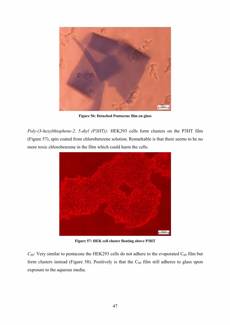
Figure 56: Detached Pentacene film on glass
Poly-(3-hexylthiophene-2, 5-diyl (P3HT)): HEK293 cells form clusters on the P3HT film
(Figure 57), spin coated from chlorobenzene solution. Remarkable is that there seems to be no
more toxic chlorobenzene in the film which could harm the cells.
Figure 57: HEK cell cluster floating above P3HT
C60: Very similar to pentacene the HEK293 cells do not adhere to the evaporated C60 film but
form clusters instead (Figure 58). Positively is that the C60 film still adheres to glass upon
exposure to the aqueous media.
47
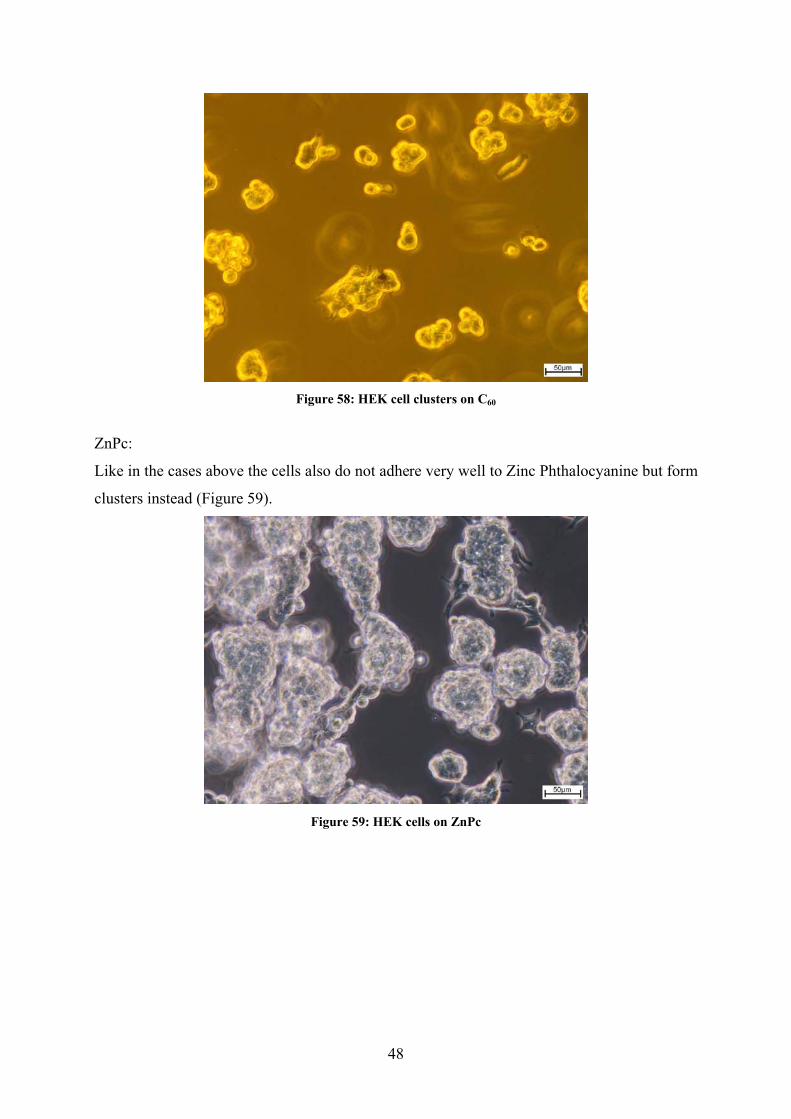
Figure 58: HEK cell clusters on C60
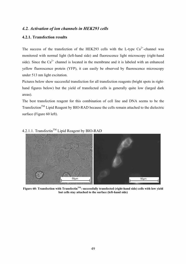
ZnPc:
Like in the cases above the cells also do not adhere very well to Zinc Phthalocyanine but form
clusters instead (Figure 59).
Figure 59: HEK cells on ZnPc
48
4.2. Activation of ion channels in HEK293 cells
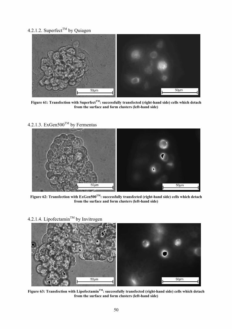
4.2.1. Transfection results
The success of the transfection of the HEK293 cells with the L-type Ca2+-channel was
monitored with normal light (left-hand side) and fluorescence light microscopy (right-hand
side). Since the Ca2+ channel is located in the membrane and it is labeled with an enhanced
yellow fluorescence protein (YFP), it can easily be observed by fluorescence microscopy
under 513 nm light excitation.
Pictures below show successful transfection for all transfection reagents (bright spots in right-
hand figures below) but the yield of transfected cells is generally quite low (larged dark
areas).
The best transfection reagent for this combination of cell line and DNA seems to be the
TransfectionTM Lipid Reagent by BIO-RAD because the cells remain attached to the dielectric
surface (Figure 60 left).
4.2.1.1. TransfectinTM Lipid Reagent by BIO-RAD
Figure 60: Transfection with TransfectinTM: successfully transfected (right-hand side) cells with low yield
but cells stay attached to the surface (left-hand side)
49
4.2.1.2. SuperfectTM by Quiagen
Figure 61: Transfection with SuperfectTM: successfully transfected (right-hand side) cells which detach
from the surface and form clusters (left-hand side)
4.2.1.3. ExGen500TM by Fermentas
Figure 62: Transfection with ExGen500TM: successfully transfected (right-hand side) cells which detach
from the surface and form clusters (left-hand side)
4.2.1.4. LipofectaminTM by Invitrogen
Figure 63: Transfection with LipofectaminTM: successfully transfected (right-hand side) cells which detach
from the surface and form clusters (left-hand side)
50
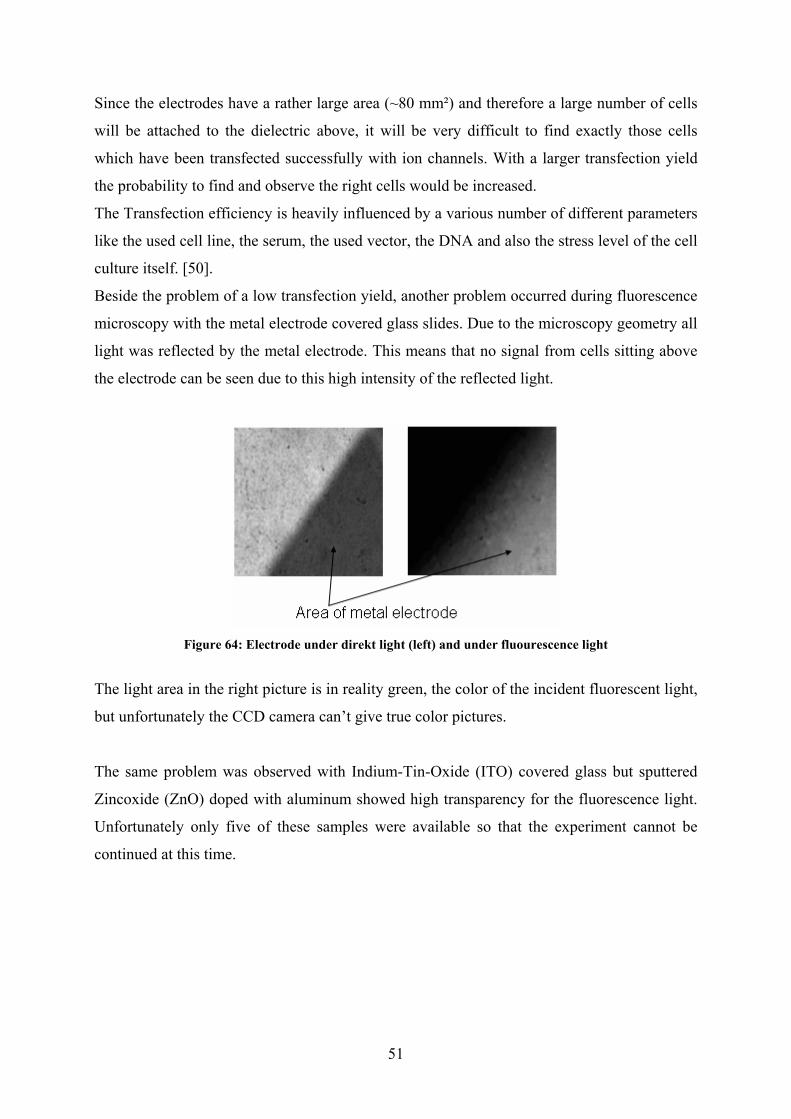
Since the electrodes have a rather large area (~80 mm²) and therefore a large number of cells
will be attached to the dielectric above, it will be very difficult to find exactly those cells
which have been transfected successfully with ion channels. With a larger transfection yield
the probability to find and observe the right cells would be increased.
The Transfection efficiency is heavily influenced by a various number of different parameters
like the used cell line, the serum, the used vector, the DNA and also the stress level of the cell
culture itself. [50].
Beside the problem of a low transfection yield, another problem occurred during fluorescence
microscopy with the metal electrode covered glass slides. Due to the microscopy geometry all
light was reflected by the metal electrode. This means that no signal from cells sitting above
the electrode can be seen due to this high intensity of the reflected light.
Figure 64: Electrode under direkt light (left) and under fluourescence light
The light area in the right picture is in reality green, the color of the incident fluorescent light,
but unfortunately the CCD camera can’t give true color pictures.
The same problem was observed with Indium-Tin-Oxide (ITO) covered glass but sputtered
Zincoxide (ZnO) doped with aluminum showed high transparency for the fluorescence light.
Unfortunately only five of these samples were available so that the experiment cannot be
continued at this time.
51
4.3. Impedance measurements
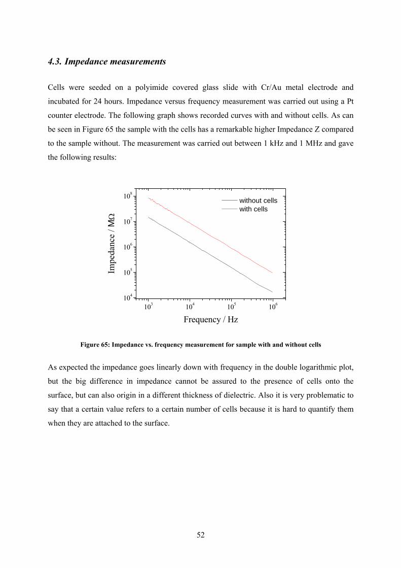
Cells were seeded on a polyimide covered glass slide with Cr/Au metal electrode and
incubated for 24 hours. Impedance versus frequency measurement was carried out using a Pt
counter electrode. The following graph shows recorded curves with and without cells. As can
be seen in Figure 65 the sample with the cells has a remarkable higher Impedance Z compared
to the sample without. The measurement was carried out between 1 kHz and 1 MHz and gave
the following results:
103 104 105 106104
105
106
107
108
without cells with cells
Impe
danc
e / M
Ω
Frequency / Hz
Figure 65: Impedance vs. frequency measurement for sample with and without cells
As expected the impedance goes linearly down with frequency in the double logarithmic plot,
but the big difference in impedance cannot be assured to the presence of cells onto the
surface, but can also origin in a different thickness of dielectric. Also it is very problematic to
say that a certain value refers to a certain number of cells because it is hard to quantify them
when they are attached to the surface.
52
53
4.4. Capacitance Measurement
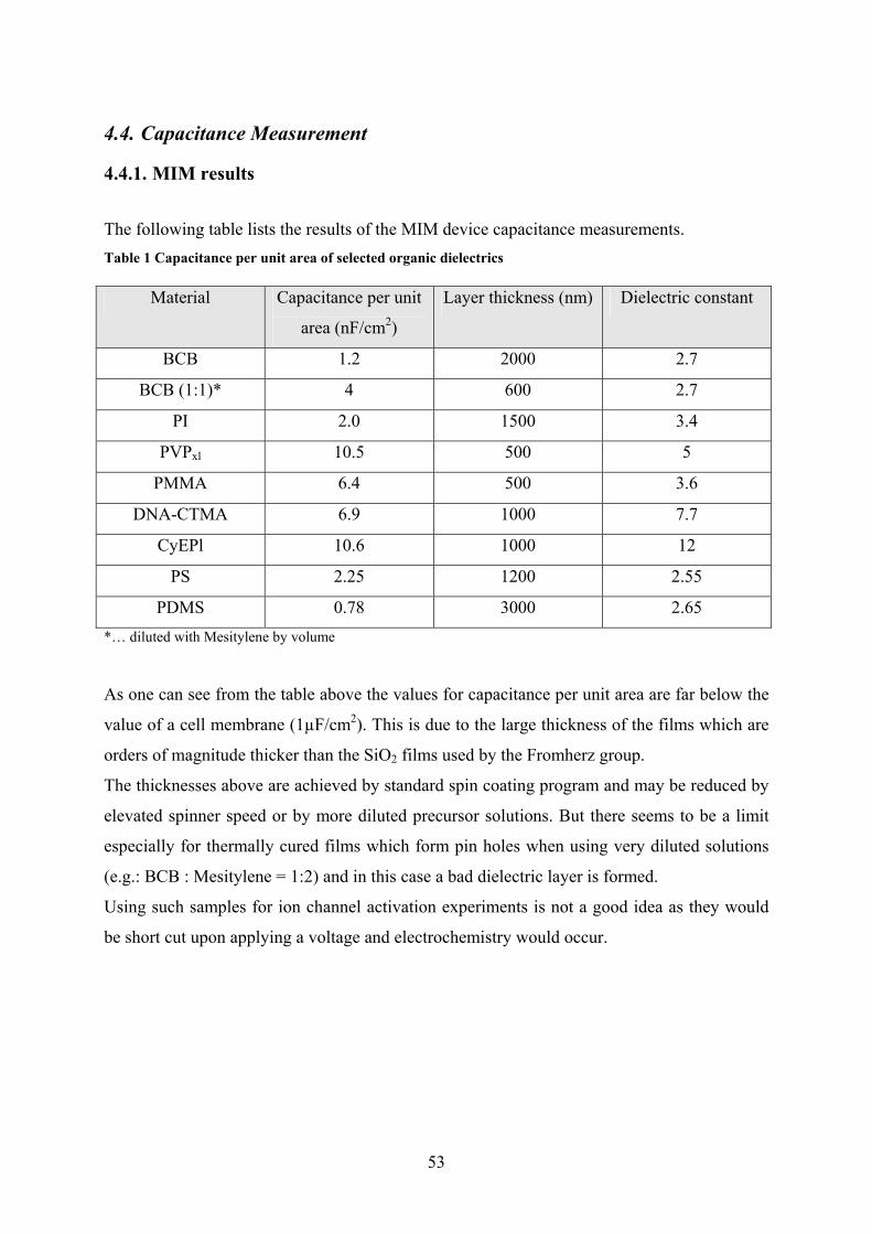
4.4.1. MIM results
The following table lists the results of the MIM device capacitance measurements. Table 1 Capacitance per unit area of selected organic dielectrics
Material Capacitance per unit
area (nF/cm2)
Layer thickness (nm) Dielectric constant
BCB 1.2 2000 2.7
BCB (1:1)* 4 600 2.7
PI 2.0 1500 3.4
PVPxl 10.5 500 5
PMMA 6.4 500 3.6
DNA-CTMA 6.9 1000 7.7
CyEPl 10.6 1000 12
PS 2.25 1200 2.55
PDMS 0.78 3000 2.65 *… diluted with Mesitylene by volume
As one can see from the table above the values for capacitance per unit area are far below the
value of a cell membrane (1µF/cm2). This is due to the large thickness of the films which are
orders of magnitude thicker than the SiO2 films used by the Fromherz group.
The thicknesses above are achieved by standard spin coating program and may be reduced by
elevated spinner speed or by more diluted precursor solutions. But there seems to be a limit
especially for thermally cured films which form pin holes when using very diluted solutions
(e.g.: BCB : Mesitylene = 1:2) and in this case a bad dielectric layer is formed.
Using such samples for ion channel activation experiments is not a good idea as they would
be short cut upon applying a voltage and electrochemistry would occur.
4.4.2. Capacitance measurement under cell influence
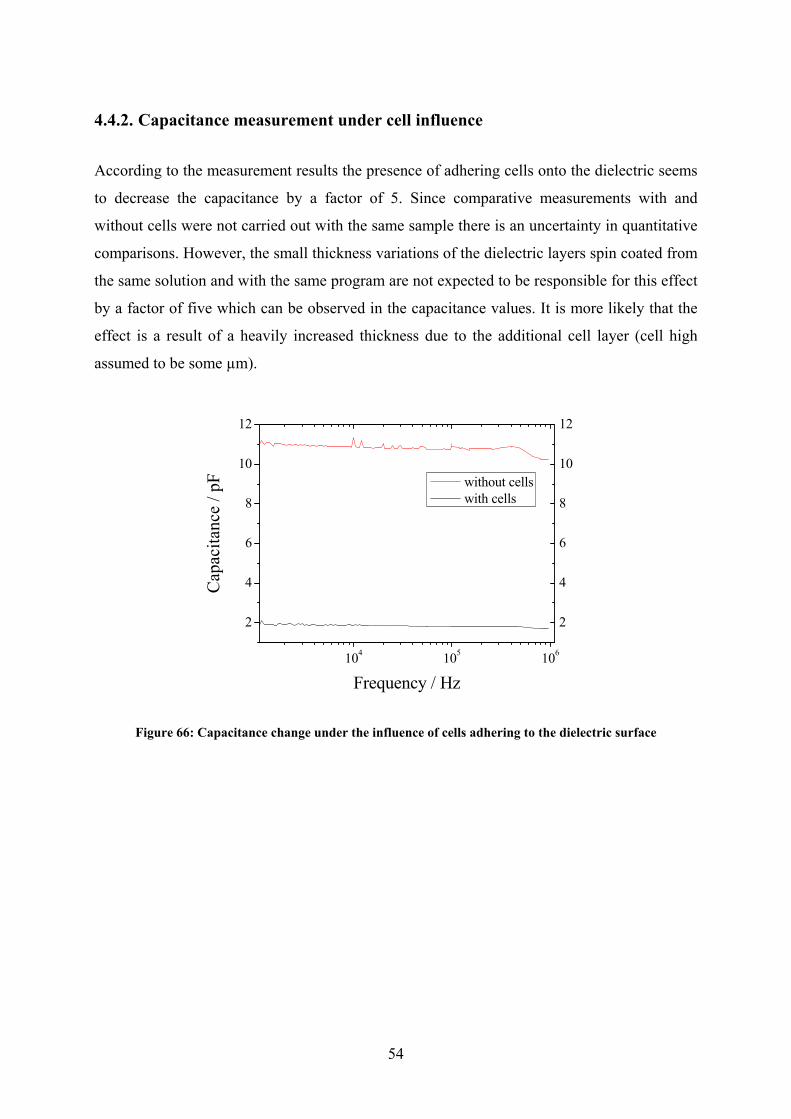
According to the measurement results the presence of adhering cells onto the dielectric seems
to decrease the capacitance by a factor of 5. Since comparative measurements with and
without cells were not carried out with the same sample there is an uncertainty in quantitative
comparisons. However, the small thickness variations of the dielectric layers spin coated from
the same solution and with the same program are not expected to be responsible for this effect
by a factor of five which can be observed in the capacitance values. It is more likely that the
effect is a result of a heavily increased thickness due to the additional cell layer (cell high
assumed to be some µm).
104 105 106
2
4
6
8
10
12
2
4
6
8
10
12
Cap
acita
nce
/ pF
Frequency / Hz
without cells with cells
Figure 66: Capacitance change under the influence of cells adhering to the dielectric surface
54
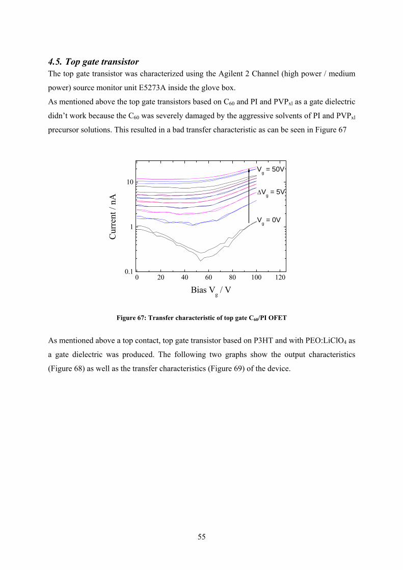
4.5. Top gate transistor The top gate transistor was characterized using the Agilent 2 Channel (high power / medium
power) source monitor unit E5273A inside the glove box.
As mentioned above the top gate transistors based on C60 and PI and PVPxl as a gate dielectric
didn’t work because the C60 was severely damaged by the aggressive solvents of PI and PVPxl
precursor solutions. This resulted in a bad transfer characteristic as can be seen in Figure 67
0 20 40 60 80 100 1200.1
1
10
Cur
rent
/ nA
Bias Vg / V
Vg = 50V
ΔVg = 5V
Vg = 0V
Figure 67: Transfer characteristic of top gate C60/PI OFET
As mentioned above a top contact, top gate transistor based on P3HT and with PEO:LiClO4 as
a gate dielectric was produced. The following two graphs show the output characteristics
(Figure 68) as well as the transfer characteristics (Figure 69) of the device.
55
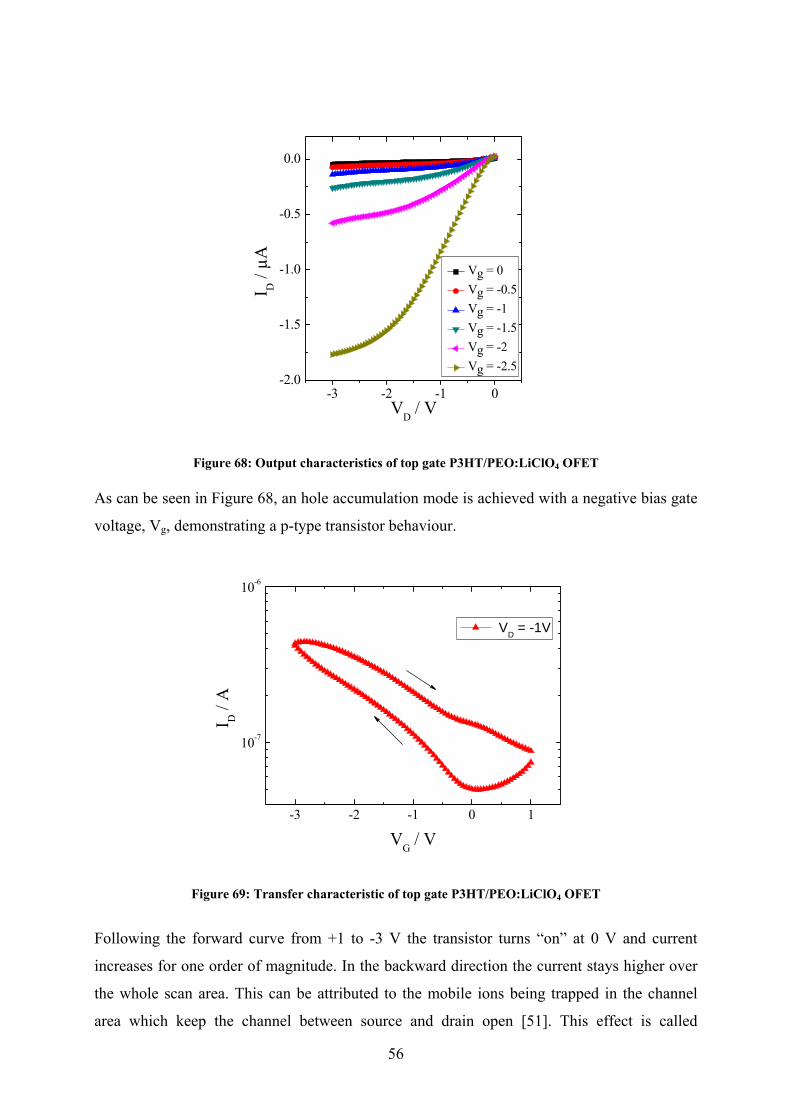
-3 -2 -1 0-2.0
-1.5
-1.0
-0.5
0.0
I D /
µA
VD / V
Vg = 0 Vg = -0.5 Vg = -1 Vg = -1.5 Vg = -2 Vg = -2.5
Figure 68: Output characteristics of top gate P3HT/PEO:LiClO4 OFET
As can be seen in Figure 68, an hole accumulation mode is achieved with a negative bias gate
voltage, Vg, demonstrating a p-type transistor behaviour.
-3 -2 -1 0 1
10-7
10-6
I D /
A
VG / V
VD = -1V
Figure 69: Transfer characteristic of top gate P3HT/PEO:LiClO4 OFET
Following the forward curve from +1 to -3 V the transistor turns “on” at 0 V and current
increases for one order of magnitude. In the backward direction the current stays higher over
the whole scan area. This can be attributed to the mobile ions being trapped in the channel
area which keep the channel between source and drain open [51]. This effect is called
56
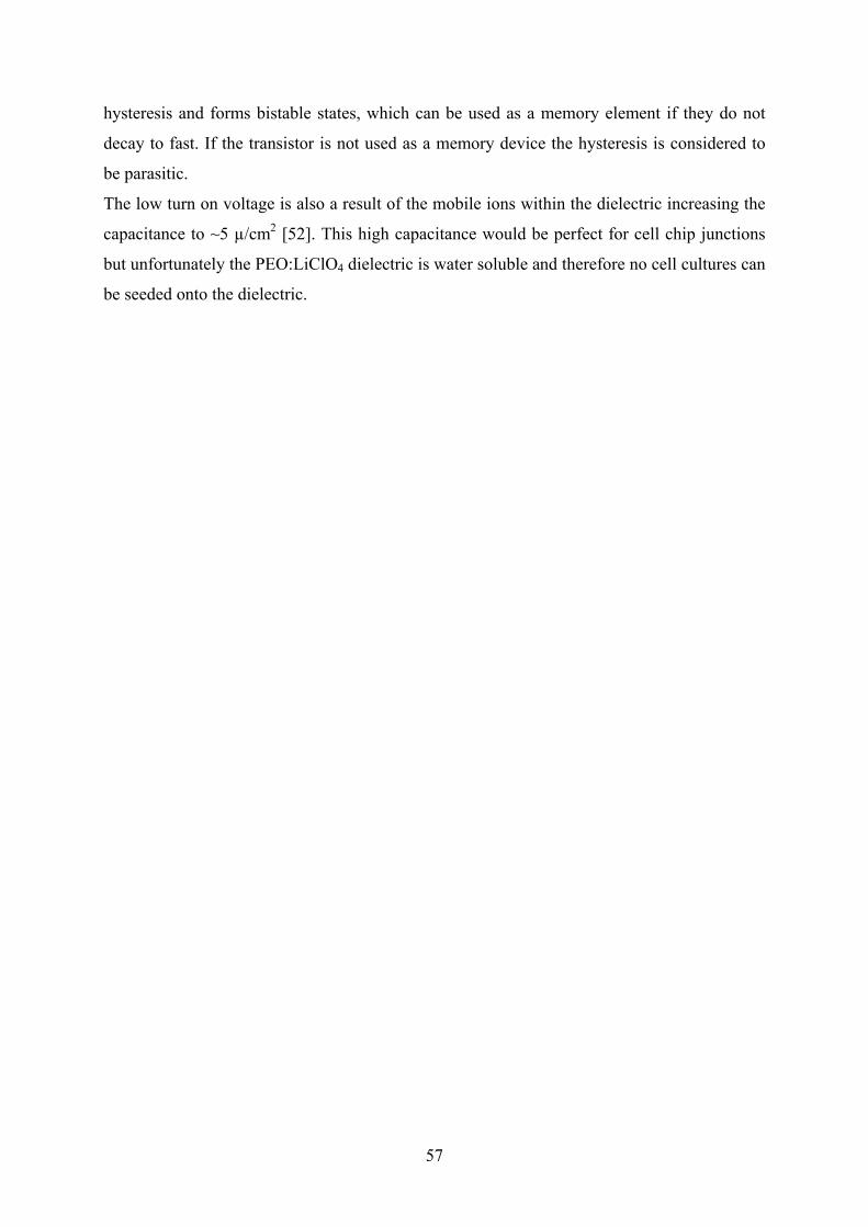
57
hysteresis and forms bistable states, which can be used as a memory element if they do not
decay to fast. If the transistor is not used as a memory device the hysteresis is considered to
be parasitic.
The low turn on voltage is also a result of the mobile ions within the dielectric increasing the
capacitance to ~5 µ/cm2 [52]. This high capacitance would be perfect for cell chip junctions
but unfortunately the PEO:LiClO4 dielectric is water soluble and therefore no cell cultures can
be seeded onto the dielectric.

58
5. Conclusions
During the course of this thesis work, feasibility of organic dielectric/ organic semiconductor
and cell adhering properties on this surfaces have been successfully investigated.
As shown in section 4.1 only on a few dielectrics the cells adhered so well that further
experiments were possible. For the semiconductor materials tested in this thesis such behavior
couldn’t be observed.
Further investigations on surface treatment and surface functionalization have to be done to
ensure a tight adherence of the HEK cell culture to the dielectric. It is to be noted that
different cell cultures behave different on various surfaces and that other cell cultures might
form a better cell organic interface and hence be more suitable for this kind of experiments.
For example, neurons could be used although they have the disadvantage that the best way to
obtain them is by dissecting them from living animals.
Another problem as mentioned above is that the fluorescence light is reflected by the metal
electrodes under the dielectric layer and therefore prohibits the ion channel activation
experiment could be avoided by changing the microscopy setup. When the excitation light
comes from above not parallel to the camera beam the ion channel activation experiment
should be possible.
To solve the problem of relative low capacitance of organic dielectric layers, experiments
with self assembled monolayers show promising capacitances with thicknesses down to
2.5nm can be achieved [53], and also a cross linking of water soluble PEO-electrolyte
dielectric has to be taken into consideration, since these layers seem to have high
capacitances, due to their high ion content.
From all this studies discussed above, it is very clear that some of the organic dielectrics and
their cell adhering properties are feasible to explore much more towards a bio – cell chip
interface.
59
6. References
1. J. Malmivuo, R. Plonsey, Bioelectromagnetism, Oxford University Press, New York,
1995, online available at: http://butler.cc.tut.fi/~malmivuo/bem/bembook/00/ti.htm
(09.10.06)
2. J. Bardeen, W.H. Braittain, Phys. Rew. 74, 232 (1948)
3. W. Shockley, Bell Syst. Tech. J., 28, 435 (1949)
4. J. E. Lilienfeld: US Patents 1,745,175 (1930), 1,877,140 (1932) & 1,900,018, (1933)
5. http://nobelprize.org/nobel_prizes/physics/laureates/1956/index.html
6. D. Kahng M. M. Attala. IRE Device Research Conference, Pittsburgh 1960
7. O. P. Hamill, A. Marty, E. Neher, B. Sakmann, F. J. Sigworth, Pflügers Arch. 391, 85
- 100 (1981)
8. P. Fromherz „Brain Online – the feasibility of a neuron silicon junction”, 20th Winter
Seminar on “Molecules, Information and Memory” Klosters 1985
http://www.biochem.mpg.de/mnphys/publications/85fro/85fro.pdf (10.10.06)
9. For a collection of references look at:
http://www.biochem.mpg.de/mnphys/publications/publications-e.html (24.10.06)
10. H. Shirakawa, E.J. Louis, A.G. MacDiarmid, C.K. Chiang, and A.J. Heeger. J. Chem.
Soc. Chem. Comm., 16, 578 – 580, (1977)
11. C.K. Chiang, C.R. Fincher Jr, Y.W. Park, A.J. Heeger, E.J. Louis, H. Shirakawa, S.C.
Gau, and A.G. MacDiarmid. Phys. Rev. Lett., 39, 1098 – 1101, (1977)
12. C.K. Chiang, M.A. Druy, S.C. Gau, A.J. Heeger, E.J. Louis, A.G. Mac-Diarmid, Y.W.
Park, and H. Shirakawa. J. Am. Chem. Soc., 100, 1013, (1978)
13. A. Heeger in: Nobel Lectures, Chemistry 1996 - 2000, Edited by: I. Grenthe, World
Scientific Publishing Co., Singapore, 2003, 380 – 417
http://nobelprize.org/nobel_prizes/chemistry/laureates/2000/heeger-lecture.html
(10.10.06)
14. Fromherz in: Nanoelectronics and Information Technology, chapter 32:
Neuroelectronic Interfacing: Semiconductor Chips with Ion Channels, Nerve Cells and
Brain. Edited by: R. Waser, Wiley-VCH, Berlin, 2003, 781 – 810
15. M. J. Schleiden, T. Schwann, M. Schulze, Klassische Schriften der Zellenlehre, Harry
Deutsch Verlag, Frankfurt am Main, 2. Auflage, 2003
16. B. Alberts, D. Bray, A. Johnson, J. Lewis, M. Raff, K. Roberts, P. Walters: Lehrbuch
der molecularen Zellbiologie, Wiley-VCH, Weinheim, 2001 2. überarbeitete Auflage

60
17. http://upload.wikimedia.org/wikipedia/de/8/80/Zelle_%28biologie%29.png (10.10.06)
18. http://upload.wikimedia.org/wikipedia/de/5/54/Doppellipidschicht.jpg (10.10.06)
19. M. F. Perutz in: Nobel Lectures, Chemistry 1942 – 1962, Elsevier Pulishing
Company, Amsterdam, 1964, 653 – 673
http://nobelprize.org/nobel_prizes/chemistry/laureates/1962/perutz-lecture.pdf
(10.10.06)
20. http://www.ks.uiuc.edu/Research/newbr/br_fig.html (10.10.06)
21. B. Alberts, D. Bray, J. Lewis, M. Raff, K. Roberts, J. D. Watson. Molecular Biology
of the Cell, Garland Publishing, Inc. New York, 2.Edition, 1983
22. D. J. Aidley, P. Stanfield, Ion Channels – Molecules in Action, Cambridge University
Press, Cambridge, UK, 1996
23. R. H. Ashley (Editor), Ion Channels – a practical approach, Oxford University Press,
Oxford, USA, 1995
24. http://genomebiology.com/2003/4/3/207/figure/F1?highres=y (10.10.06)
25. R. G. Walker, A. T. Willingham, Ch. S. Zuker, Science 287, 2229 – 2234 (2000)
26. http://www.cardiff.ac.uk/biosi/staff/jacob/teaching/ionchan/calcium_channel_structure
.jpg (10.10.06)
27. P. A. Tipler, Physik, Spektrum Akademischer Verlag, Heidelberg, Germany, 2004
28. Schoen, P. Fromherz. Appl. Phys. L., 87, 193901, (2005)
29. M. H. Ulbrich, P. Fromherz. Appl. Phys. A, 81, 887 – 891, (2005)
30. Tsumura, H. Koezuka, T. Ando. Appl. Phys. Lett. 49, 1210 – 1212 (1986)
31. B. Singh, N. S. Sariciftci. Annu. Rev. Mater. Res., 36, 199 – 230, (2006)
32. P. Fromherz, A. Offenhausser, T. Vetter, and J. Weis. Science 252, 1290 – 1293,
(1991)
33. S. M. Sze, Physics of Semiconductor Devices, J.Wiley, New York, USA, 1981
34. F. L. Graham, J. Smiley, W. C. Russel, R. Nairn. J. Gen. Virol. 36, 59 – 72, 1977
35. http://www.dow.com/PublishedLiterature/dh_003d/09002f138003dca8.pdf?filepath=c
yclotene/pdfs/noreg/618-00219.pdf&fromPage=GetDoc (10.10.06)
36. Y. Kato, S. Iba, R. Teramoto, T Sekitani, T. Someya. Appl. Phys. Lett., 84, 3789 –
3791 (2004)
37. F-Ch. Chen, Ch-W. Chu, J. He, Y. Yang. Appl. Phys. Lett., 85, 3295 – 3297 (2004)
38. L. Wang, J. Yoshida, N. Ogata, S. Sasaki, and T. Kajiyama, Chem. Mater. 13, 1273
(2001).
39. G. Zhang, L. Wang, J. Yoshida, and N. Ogata, Proc. SPIE 4580, 337 (2001).
61
40. O.Mellbring, S. Kihlman Oiseth, A. Krozer, J. Laussmaa, T. Hjertberg.
Macromolecules, 34, 7496 – 7503 (2001)
41. E. Mizuno, M. Taniguchi, T. Kawai. Applied Physics Letters, 86, 143513 (2005)
42. http://www.ncpri.ro/pullulan/en/My_Homepage_Files/Download/catalog_pull.pdf#sea
rch=%22pullulan%22 (25-09-06)
43. Dow Corning:
http://www.dowcorning.com/applications/search/default.aspx?R=131EN,(10.10.06)
44. Th. Peterbauer, J. Heitz, M. Olbrich, St. Hering. Lab on a Chip, 6, 857 – 863 (2006)
45. S. Bacchetti, F. L. Graham, Proc Natl Acad Sci U S A, 74, 1590–1594 (1977)
46. http://www.microscopyu.com/articles/livecellimaging/fpintro.html, (24.10.06)
47. W. C. Heiser, Gene Delivery to Mammalian Cells Vol. 2: Viral Gene Transfer
Techniques, Humana Press, 2004
48. http://www.fermentas.com/catalog/transfection/exgeninvitro.htm
49. http://cp.literature.agilent.com/litweb/pdf/5950-3000.pdf (10.10.06)
50. http://www1.qiagen.com/literature/qiagennews/0399/993infl.pdf
51. T. B. Singh, N. Marjanovic, G. J. Matt, N. S. Sariciftci, R. Schwödiauer and S. Bauer,
Appl. Phys. Lett., 85, 5409 (2004
52. M. J. Panzer, Chr. R. Newman, C. D. Frisbie, Appl. Phys. Lett. 86, 103503 (2005)
53. M. Halik, H. Klauk, Ute Zschieschang, G. Schmid, Chr. Dehm, M. Schütz, St. Maisch,
F. Effenberger, M. Brunnbauer, F. Stellacci, Nature, 431, 963 – 966 (2004)
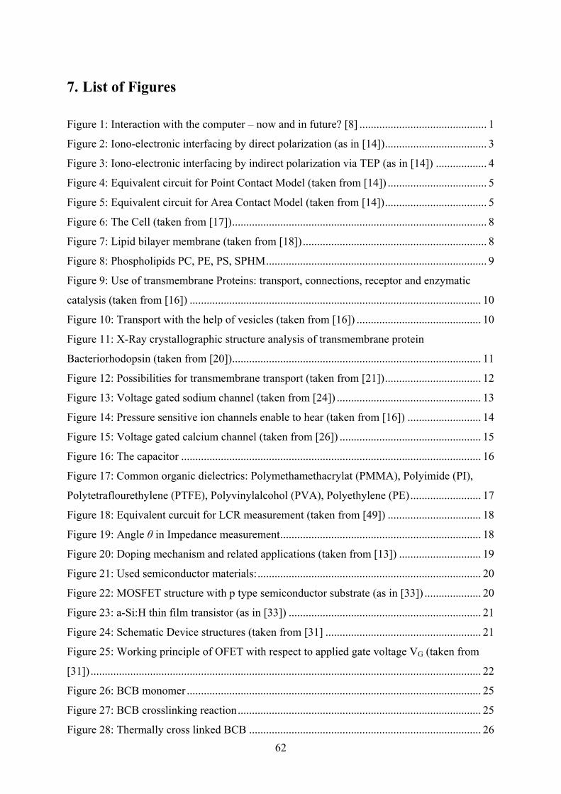
62
7. List of Figures
Figure 1: Interaction with the computer – now and in future? [8] ............................................. 1
Figure 2: Iono-electronic interfacing by direct polarization (as in [14]).................................... 3
Figure 3: Iono-electronic interfacing by indirect polarization via TEP (as in [14]) .................. 4
Figure 4: Equivalent circuit for Point Contact Model (taken from [14]) ................................... 5
Figure 5: Equivalent circuit for Area Contact Model (taken from [14]).................................... 5
Figure 6: The Cell (taken from [17]).......................................................................................... 8
Figure 7: Lipid bilayer membrane (taken from [18])................................................................. 8
Figure 8: Phospholipids PC, PE, PS, SPHM.............................................................................. 9
Figure 9: Use of transmembrane Proteins: transport, connections, receptor and enzymatic
catalysis (taken from [16]) ....................................................................................................... 10
Figure 10: Transport with the help of vesicles (taken from [16]) ............................................ 10
Figure 11: X-Ray crystallographic structure analysis of transmembrane protein
Bacteriorhodopsin (taken from [20])........................................................................................ 11
Figure 12: Possibilities for transmembrane transport (taken from [21]).................................. 12
Figure 13: Voltage gated sodium channel (taken from [24]) ................................................... 13
Figure 14: Pressure sensitive ion channels enable to hear (taken from [16]) .......................... 14
Figure 15: Voltage gated calcium channel (taken from [26]) .................................................. 15
Figure 16: The capacitor .......................................................................................................... 16
Figure 17: Common organic dielectrics: Polymethamethacrylat (PMMA), Polyimide (PI),
Polytetraflourethylene (PTFE), Polyvinylalcohol (PVA), Polyethylene (PE)......................... 17
Figure 18: Equivalent curcuit for LCR measurement (taken from [49]) ................................. 18
Figure 19: Angle θ in Impedance measurement....................................................................... 18
Figure 20: Doping mechanism and related applications (taken from [13]) ............................. 19
Figure 21: Used semiconductor materials:............................................................................... 20
Figure 22: MOSFET structure with p type semiconductor substrate (as in [33]) .................... 20
Figure 23: a-Si:H thin film transistor (as in [33]) .................................................................... 21
Figure 24: Schematic Device structures (taken from [31] ....................................................... 21
Figure 25: Working principle of OFET with respect to applied gate voltage VG (taken from
[31]) .......................................................................................................................................... 22
Figure 26: BCB monomer ........................................................................................................ 25
Figure 27: BCB crosslinking reaction...................................................................................... 25
Figure 28: Thermally cross linked BCB .................................................................................. 26
63
Figure 29: Thermally cured polyimide..................................................................................... 26
Figure 30: Crosslinked Polyvinylphenol.................................................................................. 27
Figure 31: PMMA .................................................................................................................... 27
Figure 32: CyEPl...................................................................................................................... 28
Figure 33: Polystyrene ............................................................................................................. 28
Figure 34: Polyethyleneoxide................................................................................................... 29
Figure 35: Fura-2AM molecule................................................................................................ 31
Figure 36: Ion channel activation experiment.......................................................................... 32
Figure 37:Lipid-mediated transfection in mammalian cells (taken from [46])........................ 33
Figure 38: Successfully transfected HEK293 cells (taken from [48]) ..................................... 35
Figure 39: Inverted microscope Axiovert 135 by Zeiss ........................................................... 35
Figure 40: MIM-Device ........................................................................................................... 36
Figure 41: A typical microscopic image of HEK293 cells on glass slides .............................. 39
Figure 42: Cell clustering on top of untreated BCB................................................................. 40
Figure 43: Slightly adhering cell cluster on treated BCB glass cover slide............................. 40
Figure 44: HEK293 cells on untreated polyimide.................................................................... 41
Figure 45: Cells on NaOCl treated polyimide with semitransparent Cr/Au electrode (dark
area).......................................................................................................................................... 41
Figure 46: HEK293 cells on untreated PVPxl .......................................................................... 42
Figure 47: HEK293 cells on NaClO treated PVPxl .................................................................. 42
Figure 48: HEK293 on untreated PMMA................................................................................ 43
Figure 49: HEK293 on NaClO treated PMMA, day 3 after seeding ....................................... 43
Figure 50: Maybe contaminated HEK29 cell culture on DNA-CTMA................................... 44
Figure 51: Regular structures in DNA-CTMA based HEK293 cell culure ............................. 44
Figure 52: floating HEK293 cell clusters on CyEPl ................................................................ 45
Figure 53: Cracks on PS surface .............................................................................................. 45
Figure 54: HEK293 cell clusters on Sylgard® elastomer ........................................................ 46
Figure 55: HEK293 cell cultured on Pentacene ....................................................................... 46
Figure 56: Detached Pentacene film on glass .......................................................................... 47
Figure 57: HEK cell cluster floating above P3HT ................................................................... 47
Figure 58: HEK cell clusters on C60......................................................................................... 48
Figure 59: HEK cells on ZnPc ................................................................................................. 48
Figure 60: Transfection with TransfectinTM: successfully transfected (right-hand side) cells
with low yield but cells stay attached to the surface (left-hand side) ...................................... 49

64
Figure 61: Transfection with SuperfectTM: successfully transfected (right-hand side) cells
which detach from the surface and form clusters (left-hand side) ........................................... 50
Figure 62: Transfection with ExGen500TM: successfully transfected (right-hand side) cells
which detach from the surface and form clusters (left-hand side) ........................................... 50
Figure 63: Transfection with LipofectaminTM: successfully transfected (right-hand side) cells
which detach from the surface and form clusters (left-hand side) ........................................... 50
Figure 64: Electrode under direkt light (left) and under fluourescence light........................... 51
Figure 65: Impedance vs. frequency measurement for sample with and without cells ........... 52
Figure 66: Capacitance change under the influence of cells adhering to the dielectric surface
.................................................................................................................................................. 54
Figure 67: Transfer characteristic of top gate C60/PI OFET .................................................... 55
Figure 68: Output characteristics of top gate P3HT/PEO:LiClO4 OFET ................................ 56
Figure 69: Transfer characteristic of top gate P3HT/PEO:LiClO4 OFET ............................... 56

65
8. Appendix
8.1. Appendix A – Dulbecco’s Modified Eagle Medium (GIBCO) Inorganic Salts [mg/l] Vitamins [mg/l] CaCl2.2H2O 264.0 D-Ca Pantothenate 4.0 Fe(NO3).9H2O 0.1 Cholinchloride 4.0 KCl 400.0 Folacid 4.0 MgSO4.7H2O 200.0 I-inositole 7.2 NaCl 6400.0 Nicotine amid 4.0 NaHCO3 3700.0 Pyridoxale HCl 4.0 NaH2PO4 141.0 Riboflavine 0.4 Thiamine HCl 4.0 Amino acids [mg/l] Other Components [mg/l] L-Arginine . HCl 84.0 D-Glucose 4500.0 L-Cysteine 48.0 Na-Pyruvate 110.0 L-Glutamine 580.0 Phenolred 15.0 Glycine 30.0 L-Histidine HCl.H2O 42.0 L-Isoleucine 105.0 L-Leucine 105.0 L-Lysine.HCl 146.0 L-Methionine 30.0 L-Phenylalanine 66.0 L-Serine 42.0 L-Threonine 95.0 L-Thrptophan 16.0 L-Tryosine 72.0 L-Valin 94.0
The following supplements were added to the per 500 ml media:
10 % Fetal Calf Serum (FCS)
5 ml 100x L-Glutamine
10 ml 500x Penicillin/Streptomycin:
Penicillin (50000 IU/ml)
Streptomycin (5 mg/ml)

66
8.2. Appendix B: Transfection Protocols
Note: All specifications in the protocols are for one 3.5 cm Petri dish.
8.2.1. Transfection Protocol for TransfectinTM Lipid Reagent by BIO-RAD
1. Put 200 µl Dulbecco’s MEM (without Fetal Calf Serum) in two Eppendorf tubes.
2. Pipet 1.5 µg DNA in one of the tubes.
3. Pipet 4 µl TransfectinTM Lipid Reagent into the other tube and mix it.
4. Transfer content of Tube 1 into tube 2 and gently mix it.
5. Incubate the mixture for 20 minutes at room temperature (RT).
6. Add mixture dropwise to cells in the Petri dish and gently rock the plate back and
forth and from side to side to achieve even distribution of the complexes.
7. Incubate at 37 °C for 4 hours.
8. Change medium (DMEM + FCS).
8.2.2. Transfection Protocol for SuperfectTM by Quiagen
1. Put 140 µl Dulbecco’s MEM (without FCS) in two Eppendorf tubes.
2. Add 1.5 µg DNA to one of the tubes.
3. Add 7 µl SuperfectTM Transfection Reagent to the other tube and mix it.
4. Transfer content of tube 1 to tube 2 and mix gently.
5. Incubate the mixture for 10 minutes at RT.
6. In the mean time: remove old media from Petri dish and add new DMEM + FCS
7. Add mixture dropwise to cells in the Petri dish and gently rock the plate back and
forth and from side to side to achieve even distribution of the complexes.
8. Incubate at 37 °C for 2 hours.
9. Change medium (DMEM + FCS).
8.2.3. Transfection Protocol for ExGENTM by Fermentas
1. Put 100 µl of 150 mM NaCl in an Eppendorf tube.
2. Add 1.5 µg DNA to the tube.
3. Add 3.3 µl ExGEN500TM to the tube

67
4. Immediately vortex the solution for 10 seconds.
5. Incubate the mixture for 10 minutes at RT.
6. Add mixture dropwise to cells in the Petri dish and gently rock the plate back and
forth and from side to side to achieve even distribution of the complexes.
7. Incubate at 37 °C for 4 hours
8. Change medium (DMEM + FCS)
8.2.4. Transfection Protocol for LipofectaminTM by Invitrogen
1. Put 100 µl FCS free Serum (Dulbecco’s MEM in two Eppendorf tubes
2. Add 10 µl LipofectaminTM Transfection Reagent to one of the tubes and incubated at
RT for five minutes
3. Add 1 µg of DNA to the other tube.
4. Add tube 2 to tube 1 after 5 minutes and incubated at RT for 20 minutes.
5. Add mixture dropwise to cells in the Petri dish and gently rock the plate back and
forth and from side to side to achieve even distribution of the complexes.
6. Incubate at 37° for four hours.
7. Change medium (DMEM + FCS).
8.3. Appendix C: Used equipment
• Evaporation machine UNIVEX350 (Leybold)
• Evaporation Control AS 053 (Leybold)
• Evaportaion Control IL820 (Intellemetrics)
• Glove box system MB 150 B-G/ MB 200 B (MBraun)
• Spin coater Model P6700 (Specialty Coating Systems)
• Eclipse TE200 microscope (Nikon)
• Axiovert 135 microscope (Zeiss)
• Monochromator Polychrome V (Till Photonics)
• 2 Channel (high power / medium power) source monitor unit E5273A (AGILENT
Technologies)
• HP4284A Precision LCR meter (Hewlett Packard)
• Oven (Elektron Wärme Aachen) with JUMO process controller