Embed Size (px)
Citation preview

PEOPULE’SDEMOCRATIC REPUBLIC OF ALGERIA Higher Education and Scientific
ResearchMinistry
University of Echahid Hamma Lakhdar- El-oued
Faculty of Sciences and Technology
A Dissertation Submitted to the Department of Physics
In Partial Fulfillment of the Requirements
For the Degree of Master in
Applied Physics Radiation and Energy
By:Meriem BOUHENNI
Title
Discussed on 10/06/2015
Members of jury:
Mosbah DIFALLAH MCA Universityof El-Oued President
Mohammed Sadok MAHBOUB MCA University of El-Oued Examiner
Othman BENHAOUA MAA University of El-Oued Examiner
Boubaker BENHAOUA Pr University of El-Oued Supervisor
University season: 2015 /2014
Structural and opto-electrical study of ZnO
thin films elaborated by spray pyrolysis
(home made)
N° d’ordre :
N° de série :

To... My mother & father
And Sisters & brothers
My best friends

Acknowledgements
First I would like to express my sincere gratitude to my Supervisor
Dr.Boubaker BENHAOUA
Who guided me during my work, for the opportunity, his encouragement,
patience and faith in my abilities, and without his help I would have been
wasting my time.
I am very grateful to the commission members: Dr. Mesbah DEFALAH and Dr.
Mohammed Sadok MAHBOUB, and Dr. Othman BENHAOUA for accepting
to discuss my work. It is an honor for me.
I would like to thank M.r Achour RAHAL Responsible in Laboratory(VTRS)
and M.r Ali TLIBA Responsible of Chemistry Laboratory and My brother
Lotfi.K and Youcef and My Sister Rabab, Asia, Chiama for him support to
finish this work.
Finally, I would like to thank my friends and colleagues of 1st ,2nd Master
Physics and Somia, Meriem, Rafia, Khaoula, and My Family for her support
and her confidence, and for the many sessions for discussion and exchange of the
knowledge.
Meriem BOUHENNI

List of Contents
List of Contents
List of Figures…………………………………………………………………………….. I
List of Tables……………………………………………………………………………… II
Nomenclature…………………………………………………………………………….. III
Abbreviations…………………………………………………………………………….. IV
Introduction ………………………………………………………………………………
References of Introduction……………………………………………………………….
Chapter I
I.1.Transparent conductive oxides (TCOs)……………………………………………… 6
I.2.TCOs Doping………………………………………………………………………… 7
I.3.TCOs Electrical properties…………………………………………………………… 9
I.3.1.Band gap width of TCO……………………………………………………………. 10
I.3.2.Electrical conductivity: σ (Ω cm-1.)……………………………………………… 10
I.3.3.Sheet resistance RS………………………………………………………………… 10
I.3.4.Mobility μ (cm2 / V.S)…………………………………………………………….. 10
I.4.TCOs Optical properties……………………………………………………………… 11
I.4.1.Transmission factor T……………………………………………………………….. 11
I.4.2.The reflectance R………………………………………………………………….. 12
I.4.3.Absorption factor A…………………………………………………………………. 12
I.4.4.Absorption coefficient α …………………………………………………………… 12
I.4.5.Extinction coefficient K……………………………………………………………. 12
I.4.6.Figure of merit (Ω) -1……………………………………………………………… 14
I.5.Zinc Oxide properties ……………………………………………………………….. 14
I.5.1.Crystal structure of zinc oxide……………………………………………………… 14
I.4.2.Electrical properties………………………………………………………………… 15
I.5.3.optical Properties…………………………………………………………………… 16
I.5.4. Zinc Oxide applications ………………………………………………………….. 17
I.6.Conclusion …………………………………………………………………………… 19
References of Chapter I…………………………………………………………………. 20
Chapter II
II.1.Thin Films…………………………………………………………………………… 25
II.2.Thin Film Deposition and Thin film Growth process…………………………….. 25
II.2.1.Thin film deposition processes…………………………………………………… 25
II.2.1.1.Spray pyrolysis process………………………………………………………….. 26

List of Contents
II.2.1.1.1.Principle……………………………………………………………………….. 27
II.2.1.2.Ultrasonic spray process………………………………………………………….. 27
II.2.1.3. Sol-Gel Process…………………………………………………………………. 28
II.2.1.4.Chemical Vapour Deposition…………………………………………………… 29
II.2.1.5.Pulsed-Laser Ablation Techniques…………………………………………….. 29
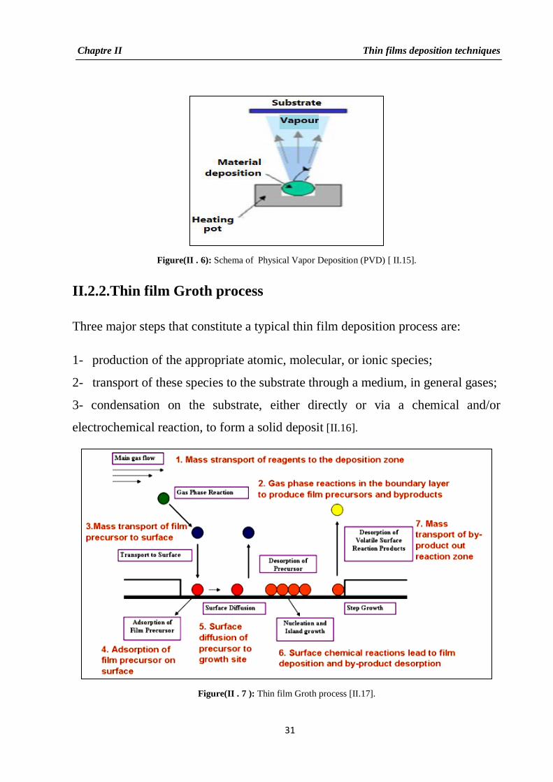
II.2.1.6.Physical Vapor Deposition (PVD)……………………………………………… 30
II.2.2.Thin film Groth process……………………………………………………………. 31
II.2.2.1.Nucleation……………………………………………………………………….. 32
II.2.2.2.coalescence………………………………………………………………………. 32
II.2.2.3.Growth……………………………………………………………………………. 32
II .3.Conclusion……………………………………………………………………………. 34
References of Chapter II………………………………………………………………… 35
Chapter III
III.1.Spray pyrolysis deposition system………………………………………………….. 38
III.1.1.Installation of experiential………………………………………………………… 38
III.1.2.Role of mounting the mounting elements The main elements are……………… 39
III.2.4.1 Experimental conditions in ZnO thin films…………………………………… 39
III.2.1. Preparation of spray solution …………………………………………………… 40
III.2.2. Preparation of ZnO Thin films…………………………………………………. 40
III.3.Characterization Techniques………………………………………………………. 40
III.3.1.optical characterization……………………………………………………………. 40
III.3.1.1.Measuring the transmittance…………………………………………………… 40
III.3.1.2.UV-Visible Spectrometer………………………………………………………. 41
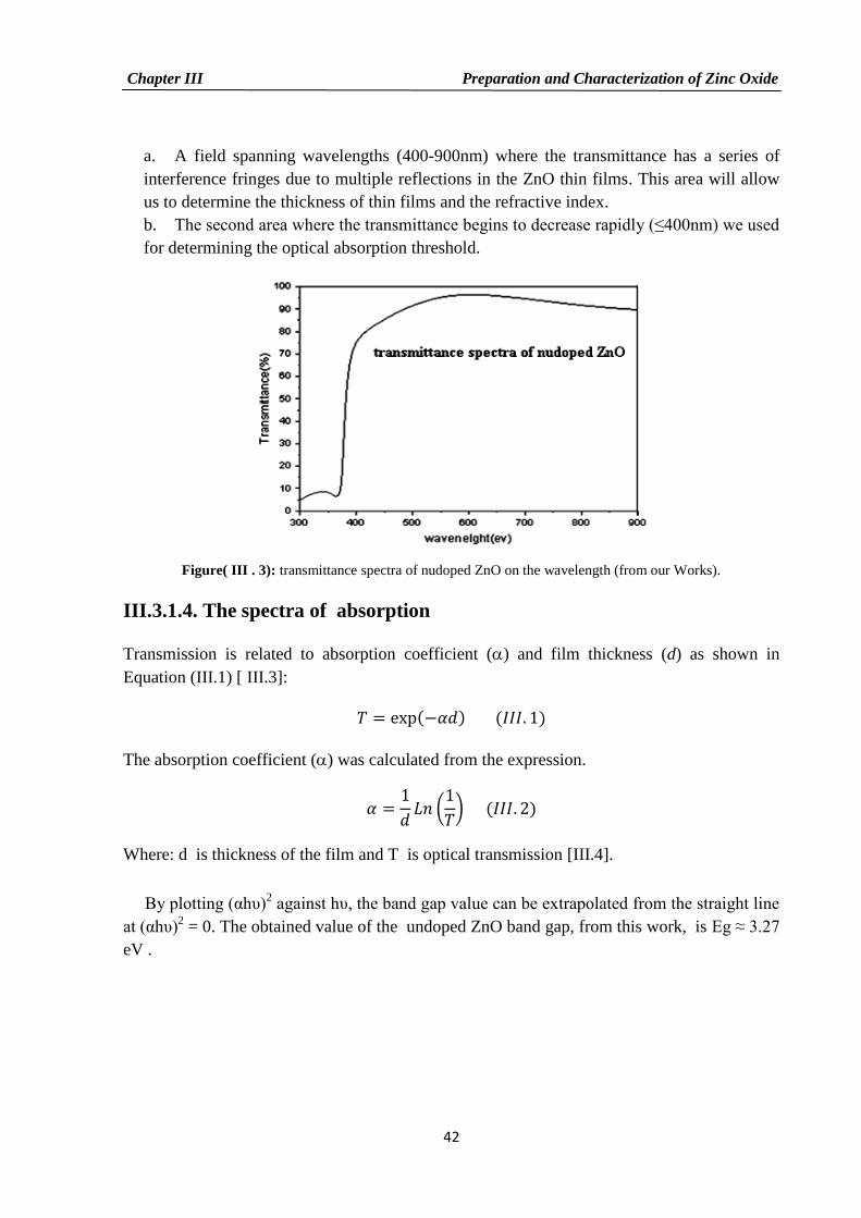
III.3.1.3.The spectra of transmittance ………………………………………………….. 41
III.3.1.4. The spectra of absorption…………………………………………………….. 42
III.3.1.5.Urbach Energy………………………………………………………………….. 43
III.3.2. Thickness of deposited thin films ………………………………………………… 43
III.3.3. Structural characterization of thin films of ZnO……………………………….. 43
III.3.3.1. X-Ray Diffraction (XRD)……………………………………………………… 44
III.3.3.2.Principle………………………………………………………………………… 44
III.4.Conclusion …………………………………………………………………………. 45
References of Chapter III……………………………………………………………….. 46
Chapter IV
IV. Result and Discussion………………………………………………………………. 48
IV.1.structural properties………………………………………………………………… 48
IV.1.1. X-Ray Diffraction……………………………………………………………….. 48
IV.1.2. Determining The lattice constant a ,c………………………………………….. 49
IV.1.3.Grain size………………………………………………………………………….. 50

List of Contents
IV.3.Optical Properties………………………………………………………………….. 51
IV.3.1.Effect of the concentration of dopant on the spectra transmittance of ZnO thin
films………………………………………………………………………………………. 51
IV.3.2.Optical gap of variation depending on the concentration of Lanthanum (La)… 52
VI.3.3.Change in energy Urbach (EUrb) depending of doping………………………… 53
IV.3.4.Determining the refractive index and the thickness……………………………. 54
IV.4.Electrical Properties………………………………………………………………… 55
IV.5.Conclusion…………………………………………………………………………. 55
References of Chapter IV………………………………………………………………. 56
Conclusion…………………………………………………………………………………
Abstract……………………………………………………………………………………
List of Figures
I
List of Figures
chapter I
Figure (I .1): Structure of bands: a) TCO undoped and b) TCO doped…………… 9
Figure (I .2): Transmission Factors, reflection and absorption of a transparent
conductive oxide……………………………………………….…….. 13
Figure (I .3): The hexagonal wurtzite structure model of ZnO…………….….…… 15
Figure (I .4): Presentation of zinc oxide gap………………………………….……. 15
Figure (I .5): Transmission of a zinc oxide film annealed at different temperatures. 16
Figure (I .6): Layer structure of thin film CIGS solar cell……………………..…… 18
Figure (I .7): Light emitting diode………………………………………………….. 19
chapter II
Figure (II . 1): Different physical and chemical thin-film deposition processes…….. 26
Figure (II . 2): Schematic of spray pyrolysis equipment……………………….…….. 27
Figure (II . 3): Sol-Gel process……………………………………………………….. 28
Figure (II . 4): Chemical vapor deposition (CVD) process…………………………... 29
Figure (II . 5): Pulsed-Laser Ablation-Based Techniques……………………………. 30
Figure (II . 6): Schema of Physical Vapor Deposition (PVD)………………………. 31
Figure (II . 7): Thin film Groth process………………………………………………. 31
Figure (II . 8): Three modes of thin film growth processes………………………….. 33
chapter III
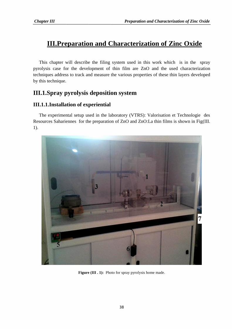
Figure (III . 1): Phot for spray pyrolysis home made………………………………… 38
Figure (III . 2) : Shows the spectral analysis of UV–Visible………………………….. 41

List of Figures
II
Figure( III . 3): transmittance spectra of nudoped ZnO on the wavelength
(from our Works)……………………………………………………..
42
Figure (III . 2) : Shows the ZnO band gap……………………………………………... 43
Figure (III . 3) : Shows the x-ray diffraction…………………………………………... 44
Figure( III . 4) : X-ray diffractometer (BRUKER - AXS type D8)……………………. 45
chapter IV
Figure (IV. 1): The X-ray diffraction patterns of undoped and La doped ZnO thin
films between (0wt.% and 20wt.%)…………………………………… 49
Figure (IV. 2): Shows the spectra optical transmission of undoped and La doped ZnO
thin films between (0wt.% and 20wt.%)………………………………. 52
Figure (IV. 3): Shows the optical band gap for pure and doped ZnO thin films………. 52
Figure (IV. 4): Shows the Urbach energy for pure and doped ZnO thin films………… 54

List of Tables
III
List of Tables
chapter I
Table (I . 1) : Other types of TCO materials………………………………………….. 8
Table (I . 2) : band gaps some TCO………………………………………………….. 10
Table (I . 3) : Minimum required properties of TCOs………………………………… 11
Table (I . 4) : Physical properties of ZnO…………………………………………….. 17
chapter IV
Table(IV. 1): shows the interlinear spacing (dhkl) and lattice constants a, c and c/a of
the undoped and La doped ZnO thin films between (0wt.% and
20wt.%)………………………………………………………………… 50
Table(IV. 2): shows the crystallite size of the undoped and La doped ZnO thin films
between (0wt.% and 20wt.%)…………………………………………. 51
Table(IV. 3): The band gape of pure and doped ZnO thin films……………………… 53
Table(IV. 4): The Urbach energy of pure and doped ZnO thin films…………………. 54
Table(IV. 5): Refractive index and thickness doped ZnO (0-20w%)………………… 55

Nomenclature
IV
Nomenclature
Eg Chemical activity
Eg0 the band-gap of the undoped semiconductor
m*
cv effective mass
α the absorption coefficient
h the Plank’s constant
ν the frequency of incident radiation
K extinction coefficient
n the density of free carriers
µ mobility
e
ρ resistivity
Rs Sheet resistance
τ carrier life time between two collisions
m* effective mass
T Transmittance factor
ФT intensity of the transmitted light
Ф0 intensity of light incident on surface.
R Reflectance factor
ФR intensity of light
A Absorption factor
ФA intensity of absorption
λ wavelength
n the complex refractive index
i the square root of -1
n the refractive index
k the absorption index
c Speed of light

Nomenclature
V
λp plasma wavelength
τ the carrier relaxation time
ε0 the permittivity of free space
wp the plasma frequency
TC Figure of merit
d thickness of the film
EU the Urbach energy
dhkl interlinear spacing
θ the Bragg angle
n the order of the spectrum
α, c the lattice parameters
hkl the Miller indices of the planes
G Crystallite size (nm)
β width at half maximum intensity

Abbreviations
VI
Abbreviations
TCO Transparent Conductive Oxides
CdO Cadmium Oxide
SnO2 Tin Oxide
ZnO Zinc Oxides
La Lanthanum
ITO Indium Tin Oxide
ZTO Zinc doped tin oxide
TiO2 Titan oxide
AZO Aluminum doped Zinc oxide
LEDs Light-Emitting Diode
PL Photoluminescence
VIS Visible
PVD Physical vapor deposition
MBE Molecular Beam Epitaxy
PLD Pulsed laser deposition
CVD Chemical vapor deposition
PVD Physicall vapor deposition
MBE Molecular Beam Epitaxy
VW Volmer-Weber
FV Frank-Van
SK Stranski-Krastanov
VTRS Valorisation et Technologie des Resources Sahariennes
UV-VIS Ultraviolet and Visible
XRD X-Ray Diffraction
JCPDS Joint Committee on Powder Diffraction Standards
FWHM width at half maximum intensity
wt. % Weight percentage (La%)

Introduction

Introduction
Introduction
The studies carried on transparent conductive oxides (TCOs) attracted the attention of
many researchers because of their various applications. thanks to their double property,
electrical conductivity and transparency in the visible average.
Thanks to their specific structural, electrical and optical properties as a thin film of
transparent conductive oxides [1], major efforts have been made in this area in recent years
for their multiple applications. Their fields of application are very broad; they are found in
areas such as electronics [2], optoelectronics [3], the photo thermal conversion [4], the
photovoltaic conversion [5], etc ... These materials evoke great importance from the point of
plant view, Among these compounds, one is zinc oxide (ZnO) [6].
In the past ten years we have witnessed a revival of, and subsequent rapid expansion in, the
research on zinc oxide (ZnO) as a semiconductor. The high electron mobility, high thermal
conductivity, wide and direct band gap and large exciton binding energy make ZnO suitable
for a wide range of devices, including transparent thin-film transistors, photodetectors, light-
emitting diodes and laser diodes that operate in the blue and ultraviolet region of the
spectrum.
The deposit of zinc oxide doped films is the subject of much research because of these
multiple potential applications. Studies conducted in recent years on the applications of
semiconductors show a general trend towards miniaturization and nanotechnology.
Thin films have, in this sense, a special interest in the resolution of problems of the present,
since they allow to offer savings in material and workforces, relieve congestion and achieve
high flexibility.
Several techniques are used to obtain zinc oxide films, but the various methods have
technical constraints for filing sufficiently homogeneous layers. Note that the physical
properties of thin films strongly depend on the operating conditions and the method of
preparation. A new technique for depositing thin films has been explored: the spray pyrolysis
process. This method has several advantages: possibility of using precursors of high purity

Introduction
deposit facility on substrates of large surfaces and complex shapes at High temperatures and
with low cost.
The objectives of this work are, firstly to control the development of ZnO thin films undoped
and doped Lanthanum (ZnO: La), to study their electrical, optical and structural properties
obtained by this method.
This work is focused on the development and characterization of La doped ZnO thin films
deposited on glass substrates in order to develop transparent conductive oxides (TCO) by the
technique mentioned above. For the preparation of ZnO, zinc acetate solution is used as a
source of zinc as a precursor dissolved in bidistilled water and methanol (as starting solution)
and La trichloride as a dopant. Our study will focus on the mastery of technical spray
pyrolysis and will focus primarily on the effect of the concentration of dopant on the
structural and optoelectronic properties of ZnO thin films.
This work consists of four chapters and a general conclusion. In the first chapter (CH I)
general context ,of the study, will be recalled as well as thin films and the physical properties
of transparent conductive oxides, such as zinc oxide and the effect of dopants for modify the
physical properties of these thin films. Also their fields of applications will take place in this
chapter. In the second chapter (CH II) we will present the different techniques used to develop
thin films used in this study. The spray porolysis process will be explained in the third chapter
(CH III). The description of various stages of development of thin films of zinc oxide will
take place in this section. The devices, used in this study to characterize these layers will be
described in this chapter. The fourth chapter (CH IV) is devoted to the presentations of
experimental results and their discussion. Finally, we conclude this dissertation with a general
conclusion on these results.

Introduction
References of Introduction
[1] T. Karasawa, Y. Miyata, Thin Solid Films 223 (1993) 135-139.
[2] Yi Hu, S.-H. Hou, Mate. Chem. Phys 86 (2004) 21-25.
[3] Pietro Siciliano, Sensors and Actuators B 70 (2000) 153-164.
[4] Jianrong Zhang and Lian Gao, J. Solid. St. Chem 177 (2004) 1425-1430.
[5] R. Tala- ighil, M.S. Belkaid, A. Maallemi, K. Melhani, A. Iratni, M. Boumaour, J. Solar
Eng. Mater & Solar cell (2005) 1-11.
[6] A. Tibercio- Silver, J.C. Joubert et M. Labeau. J. Phys. III France 2 (1992) 1287-1303.
Chapter I
Transparent Conductive Oxides
(TCOs)

Chapter I Transparent Conductive Oxides
6
I. Transparent Conductive Oxides
This chapter focuses on some properties and applications of transparent conductive oxides
(TCO), and some properties of zinc oxide (crystallographic, optical, ...) and the application of
zinc oxide.
I.1. Transparent Conductive Oxides (TCOs)
TCO is a wide band-gap semiconductor [I .1].Transparent conductive oxides (TCO) have
high optical transmission at visible wavelengths [I.2] (400 nm < λ < 800 nm) [I .3] and
electrical conductivity close to that of metals. They also reflect near infrared and infrared (i.e.,
heat) wavelengths [I.2].
The history of TCO starts from 1907, with the discovery of Cadmium Oxide (CdO) thin
film by a German scientist Karl Baedeker [I.4]. The first TCO patents for undoped and doped
tin oxide (SnO2) films were filed respectively in 1931 and 1942. Such films were employed as
aircraft windshield deicers in World War II. The following decades saw the development of
In2O3-
and ZnO-based TCOs [I.5]. Tin oxide (SnO2) was first deposited on glass by pyrolysis
and CVD in the 1940s for electroluminescent panels. Since then, applications and deposition
processes have mushroomed [I.2].
The ZnO varistors were first developed in Japan by Matsuoka[I.6] and his research group
in 1968 and commercialized in the following year. In the first decade after their invention
various additives improving the electrical characteristics were discovered and the processing
conditions were optimized. In the next decade, the microstructures and the physical properties
of the grain boundaries were gradually identified. At that time applications grew in protection
of electrical equipment and electronic components such as transistors and ICs against voltage
surges. In 1988 almost 100 % of the lightning arresters produced in Japan were ZnO varistors
[I.7].
All TCOs can be classified into two major classes; n-type and p-type[I.8]. The ZnO is
changed in conductivity from n-type to p-type based on doping [I.9].
TCO’s are generally n-type wide bandgap semiconductors (although p-type materials are now
being developed) with a relatively high concentration of free electrons in the conduction band

Chapter I Transparent Conductive Oxides
7
[I.2] . No p-type TCO was reported until 1993 due to the localization behavior of the induced
holes for p-type TCO fabrication [I.10].
TCOs are used in a wide range of applications, electrochromic smart windows, transparent
contacts for solar cells, optoelectronic devices, flat panel displays, liquid crystal devices [I.2],
touch screens, gas sensors, organic light-emitting diodes [I.8].
I.2.TCOs Doping
TCOs are degenerates n-type conductors (metal-type conductivity) [I.5]. TCOs thin films
electrical conductivity is essentially due to the non-stoichiometry of these materials which
indicated that oxygen vacancies in the synthesis of these thin films. These gaps increase the
conduction, in other hand they create in the conduction band levels ionized [I.11].
The property of semiconductors that makes them most useful for constructing electronic
devices is that their conductivity may easily be modified by introducing impurities into their
crystal lattice. The process of adding controlled impurities to a semiconductor is known as
doping. The amount of impurity, or dopant, added to an intrinsic (pure) semiconductor varies
its level of conductivity. Doped semiconductors are often referred to as extrinsic. By adding
impurity to pure semiconductors, the electrical conductivity may be varied not only by the
number of impurity atoms but also, by the type of impurity atom and the changes may be
thousand folds and million folds.
Introducing impurity atoms into a semiconductor host leads to different changes in
different properties due to crystal size effects; formation of different phases etc. and in case of
electrical properties, there is an increase in the free-carrier concentration. In n-type
semiconductors, free electrons in the conduction band are majority charge carriers, whereas
holes in the valence band are majority carriers in p-type semiconductors. Shallow donors and
acceptors have a much smaller ionization energy compared to the band gap energy of the host
semiconductor; hence, they can readily contribute to electrical conductivity [I.12][ I.13]. The
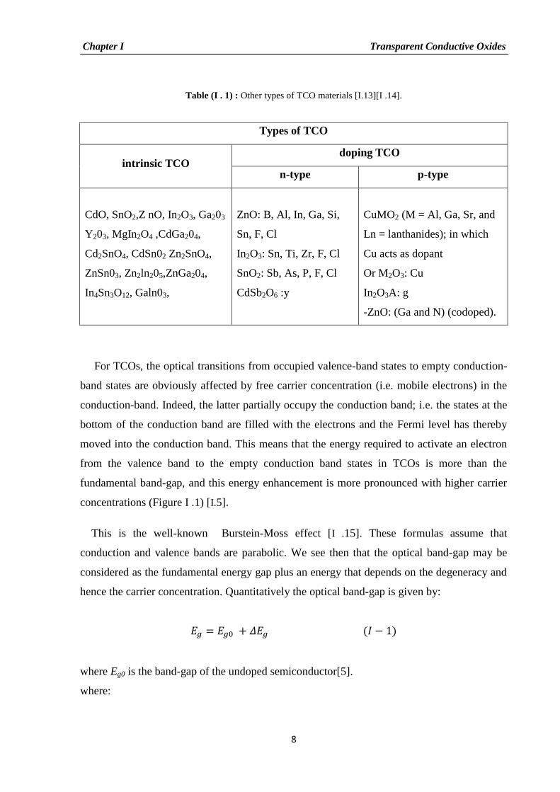
table(I.1) shows the TCO intrinsic and doping n-type and p-type.
Chapter I Transparent Conductive Oxides
8
Table (I . 1) : Other types of TCO materials [I.13][I .14].
Types of TCO
intrinsic TCO doping TCO
n-type p-type
CdO, SnO2,Z nO, In2O3, Ga203
Y203, MgIn2O4 ,CdGa204,
Cd2SnO4, CdSn02 Zn2SnO4,
ZnSn03, Zn2ln205,ZnGa204,
In4Sn3O12, Galn03,
ZnO: B, Al, In, Ga, Si,
Sn, F, Cl
In2O3: Sn, Ti, Zr, F, Cl
SnO2: Sb, As, P, F, Cl
CdSb2O6 :y
CuMO2 (M = Al, Ga, Sr, and
Ln = lanthanides); in which
Cu acts as dopant
Or M2O3: Cu
In2O3A: g
-ZnO: (Ga and N) (codoped).
For TCOs, the optical transitions from occupied valence-band states to empty conduction-
band states are obviously affected by free carrier concentration (i.e. mobile electrons) in the
conduction-band. Indeed, the latter partially occupy the conduction band; i.e. the states at the
bottom of the conduction band are filled with the electrons and the Fermi level has thereby
moved into the conduction band. This means that the energy required to activate an electron
from the valence band to the empty conduction band states in TCOs is more than the
fundamental band-gap, and this energy enhancement is more pronounced with higher carrier
concentrations (Figure I .1) [I.5].
This is the well-known Burstein-Moss effect [I .15]. These formulas assume that
conduction and valence bands are parabolic. We see then that the optical band-gap may be
considered as the fundamental energy gap plus an energy that depends on the degeneracy and
hence the carrier concentration. Quantitatively the optical band-gap is given by:
where Eg0 is the band-gap of the undoped semiconductor[5].
where:

Chapter I Transparent Conductive Oxides
9
Figure( I . 1) : Structure of bands: a) TCO undoped and b) TCO doped [I.16].
The energy gap was estimated by assuming a direct transition between valence and
conduction bands from the expression:
Where: α the absorption coefficient, h the Plank’s constant, ν the frequency of incident
radiation, K is a constant, and Eg is the band gap energy, determined by extrapolating the
straight line portion of the spectrum to [I.17][ I.18].
I.3.TCOs Electrical properties
Transparent conductive oxides (TCO) belong to the group of wide band gap
semiconductors [I.14].
The early work on the electrical properties of TCO films has been reviewed by many
workers[I.5].

Chapter I Transparent Conductive Oxides
10
I.3.1.Band gap width of TCO
Transparent conductive oxides (TCO) belong to the group of wide band gap
Semiconductor[I.14] [I.19].
Table (I. 2) : band gaps some TCO.
TCO Gap(eV)
ZTO >3
ZnO (3.2 – 3.3)
TiO2 (3 – 3.2)
SnO2 (3.6 – 4.2)
ITO 4.2
I.3.2.Electrical conductivity: σ (Ω cm-1
.)
The conductivity σ is a product of the number of charge carriers n in a material, the
electrical conductivity of such materials is given by:
Where: n is the density of free carriers, µ is their mobility, e is the electronic charge, and The
resistivity ρ is defined as the inverse of the conductivity [I.20].
I.3.3.Sheet resistance RS
while sheet resistance can be related to electrical conductivity () and film thickness (t) as
shown in Equation [I.3]:
I.3.4.Mobility μ (cm2 / V.S)
The charge carrier mobility (μ), normally measured in cm2/V·s, is related to the relaxation
time (τ) and the effective mass of the charge carriers (m* ) according to:

Chapter I Transparent Conductive Oxides
11
Where: τ is the carrier life time between two collisions and the effective mass, m* is defined
by the mass that charge carrier seems to carry, usually stated in units of the ordinary mass of
an electron me (9.11×10⁻³¹
kg) [I.5].
Table (I . 3): Minimum required properties of TCOs [I.21].
Parameters Transparent Conductive Materials
Band gap
Transparency at 550nm
Resistivity
Carrier Concentration
Mobility
Sheet resistance
>3.1eV (380nm)
>90% (for n-type) and >85% (for p-type)
10-4
cm (for n-type) and 10-3
cm (for p-type)
>1020
cm-3
(for n-type) and >1018
cm-3
(for p-type)
>40cm2(V s)
-1( for n-type) and >20cm
2(V s)
-1 (for p-type)
≤ 10kΩ /square (for 20nm thickness)
I.4.TCOs Optical properties
The light from the source is transferred by optics in the instrument and strikes the surface
of the sample, where the light is divided into three parts : transmission (T), reflection (R) and
absorption (A) [I.22].
I.4.1.Transmission factor T
This optical magnitude is defined as follows:
%
Where: (ФT) the intensity of the transmitted light and (Ф0) the intensity of light incident on its
surface.

Chapter I Transparent Conductive Oxides
12
I.4.2.The reflectance R
The reflectance of a material is the intensity of light (ФR) which is reflected at its surface
with respect to the incident light intensity (Ф0).
%
I.4.3.Absorption factor A [I.19]
%
The sum of the three parts should be equal to the input light. Therefore, a formula can be
written, as follows if we assume the sum of input light is[I.22]:
I.4.4.Absorption coefficient α
The Beer-Lambert law is used to connect the flux transmitted through the distance d to the
absorption coefficient α by the following equation [I.19]:
I.4.5.Extinction coefficient K
The extinction coefficient K which is defined as the amount of loss in energy due to the
interaction between light and charges of the medium was calculated for all the thin films
prepared from the following relationship :
Where: λ is wavelength (nm) [I.23].
Determining the refractive index, n, and the absorbance (absorption coefficient), k, of a
coating are two important parameters in thin film research. In real materials, the polarization

Chapter I Transparent Conductive Oxides
13
does not respond instantaneously to an applied field. This causes dielectric loss, which can be
expressed by the complex index of refraction that can be defined:
where: n is the complex refractive index, i is the square root of -1, n is the refractive index,
,and k is the absorption index
Both n and k are dependent on the wavelength. In most circumstances k > 0 (light is
absorbed).
The absorbance, refractive index, and film thickness of thin films can be calculated from
the spectral data[I.24]. The Figure(I.2)represents the evolution of the transmission factors,
reflection and absorption, depending on the wavelength, with a thin layer of TCO.
Figure( I . 2): Transmission Factors, reflection and absorption of a transparent conductive oxide.
The first wavelength, λg, separates the absorption zone in the ultraviolet from the
transparent zone in the visible. It corresponds to the threshold of inter-band absorptions and it
is correlated to the optical band-gap, Eg, according to [I.5]:
The second wavelength, λp (generally called plasma wavelength), corresponds to the front
rise of the reflectivity in the IR and accounts for a metallic character of the TCO, it
corresponds to intraband absorption in the conduction band of the electrode material, when

Chapter I Transparent Conductive Oxides
14
resonance occurs between the incident electromagnetic radiation and the plasma oscillation of
the (quasi) free electrons in the conduction band. λp depends on the concentration of these
electrons in the conduction band (N)and on their mobility (μ) according to:
Where: τ is the carrier relaxation time, ε0 is the permittivity of free space, and ε∞ is the high
frequency dielectric constant of the involved media [I.5].
A term introduced here is plasma wavelength, λp, which corresponds to the plasma
frequency when optical properties change radically.
When λ > λp, the film exhibits reflectance properties,
Whereas at λ < λp the high transparency occurs.
However, λp moves to shorter wavelengths with the increase of carrier density or
concentration [14].
I.4.6.Figure of merit (Ω) -1
Many important factors must be considered when selecting a TCO material for each of the
applications identified above. Haacke [I.8, I.10] introduced a figure of merit, TC, to evaluate
transparent conducting materials. In general, TC is defined as seen in this Equation:
where : T is optical transmission (fraction) ,and RS is sheet resistance [I.3].
I.5.Zinc Oxide properties
I.5.1.Crystal structure of zinc oxide
ZnO crystallizes in the hexagonal wurtzite structure in which the oxygen atoms are
arranged in a hexagonal close-packed type of lattice with zinc atoms occupying half the
tetrahedral sites (see Figure I . 3). The two types of atoms, Zn and O [I.25].
The mean lattice constants are a = 3.250 Å and c = 5.206 Å, depending slightly on
stoichiometry deviation. O-2
(1/3; 2/3; z), (1/3; 2/3; 0) with z= 0, 38 [I.19].

Chapter I Transparent Conductive Oxides
15
Figure( I . 3): The hexagonal wurtzite structure model of ZnO [I.26].
I.5.2.Electrical properties
ZnO is a wide-gap semiconductor with a direct gap around 3.4 eV (i.e. in the near-UV)
[I.27]. since the minimum of the conduction band and the maximum of the valence band are
located on the same axis Γ.
Fig (I . 4): Presentation of zinc oxide gap [I.28].
A good transparent conducting oxide is characterized by high-electrical conductivity and
optical transparency. ZnO in its pure form is an insulator. The doping of TCO used to
improve their electrical properties. Zinc oxide (ZnO) changed in conductivity from n-type to
p-type based on doping [I.8].

Chapter I Transparent Conductive Oxides
16
n-type doping : La, Al, Ga, In.
p-type doping: Li, Na, K, Cu, Ag. N, P, As [I.19].
I.5.3.optical Properties
The zinc oxide ZnO is a transparent material, the refractive index varies between 1.9 and
2.2[28]. It exhibited an absorption at around 360 nm wavelength in the ultraviolet, which
accounts for the value of the gap of the thin films of this material. By cons, it is transparent in
the visible and near infrared spectrum as shown in Figure(I . 5).
Figure( I . 5): Transmission of a zinc oxide film annealed at different temperatures [I.29].
The optical properties of TCOs also depend on doping and oxygen vacancies. In addition
to the zinc oxide transparent properties, this material also has the luminescence property.
Under the effect of a light beam of energy greater than the gap of ZnO, zinc oxide emits
photons. These photons generally have a wavelength of about 550 nm corresponding to green
light [I.30].
The table(I.4) summarizes some of the characteristics of zinc, structural, electrical and
optical.

Chapter I Transparent Conductive Oxides
17
Table( I . 4): Physical properties of ZnO [26].
Properties ZnO
Lattice parameters at 300 K
—a0 (nm)
—c0 (nm)
Density (g/cm3)
Stable phase at 300 K
Melting point (°C)
Thermal conductivity (Wcm−1
°C
−1)
Linear expansion coefficient (°C)
Static dielectric constant
Refractive index
Band gap (RT)
Band gap (4 K)
Exciton binding energy (meV)
Electron effective mass
Electron Hall mobility at 300 K (cm2/Vs)
Hole effective mass
Hole Hall mobility at 300 K (cm2/Vs)
0.32495
0.52069
5.606
Wurtzite
1975
0.6, 1-1.2
a0: 6.5 cm3 × 10−6
c0: 3.0 cm3 × 10−6
8.656
2.008
3.370 eV
3.437 eV
60
0.24
200
0.59
5–50
I.5.4. Zinc Oxide applications
Because of its diverse properties, both chemical and physical, zinc oxide is widely used in
many areas. It plays an important role in a very wide range of applications [I.31].
Zinc oxide is a new and important semiconductor which has a range of applications in
electronics and electrotechnology [I.32]. Its wide energy band (3.37 eV) and high bond energy
(60 meV) [I.33] at room temperature mean that zinc oxide can be used in photoelectronic
[I.34] and electronic equipment [I.35], in devices emitting a surface acoustic wave [I.36], in
field emitters [I.37],in sensors [I.38], in UV lasers [I.39], and in solar cells [I.40].
Thin Film Solar Cells
ITO is the most important and widely used thin film TCO. However, dwindling world
indium supplies is a worry, and as a result, there is an effort to replace ITO due to the indium
used in this material. To this end, ZnO and AZO are now being used as transparent electrical

Chapter I Transparent Conductive Oxides
18
contacts in thin film CIGS and silicon solar cells [I.41]. The AZO films obtained at higher
powers have good transparency in visible region. The film with lowest resistivity of 6.67 x 10-
4 cm and transparency greater than 90% was obtained at deposition power of 175 W and
substrate temperature of 200 °C after vacuum annealing at 400 °C.
Figure (I . 6): Layer structure of thin film CIGS solar cell [I.42].
UV Laser
Room temperature of ZnO-nanowire-based UV lasing has been recently demonstrated
[I.43]. The typical room temperature photoluminescence (PL) spectrum of ZnO nanorods with
an excitation wavelength of 325 nm at room temperature [I.44]. The spectrum exhibits two
bands including a strong ultraviolet emission at 378 nm (or 3.28 eV) and a weak spectral band
in the visible region. The UV emission was contributed to the near band edge emission of the
wide band gap of ZnO. Visible emission is due to the presence of various point defects such
as oxygen vacancies.
Light-Emitting Diode
The output power of GaN LEDs with ZnO nanotip arrays can be enhanced by up to 50%
times [I.45]. A heterojunction LED could be fabricated by the growth of vertically aligned
ZnO nanowires on a p-GaN substrate and employed indium tin oxide (ITO)/glass to combine
and package [46, 47]. Figure shows the. Most of the currently developed ZnO LEDs are
based on heterojunctions. However, a ZnO rod p-nhomojunction LED with an ion-implanted
P-doped p-type ZnO could also be fabricated [I.48].

Chapter I Transparent Conductive Oxides
19
Figure( I . 7): light emitting diode.
I.6. Conclusion
Zinc oxide is considered the family of transparent conductive oxides, and also, it has very
interesting properties, it is available to be introduced for the several components, in addition,
it is inexpensive, piezoelectric, good driver, absorbent, catalyst, non-toxic. ZnO applications
are very wide ranging from photovoltaic to detection systems, and it is therefore a key
material for the technological development that we lemons in the next chapter, the most
important processes applied to form a thin film.

Chapter I Transparent Conductive Oxides
20
References of Chapter I
[I.1] T.J. Coutts, J.D. Perkins, and D.S. Ginley T.O. Mason, '' Transparent Conducting
Oxides: Status and Opportunities in Basic Research'', Presented at the 195th Meeting
of the Electrochemical Society Seattle, Washington May 2-6, 1999.
[I.2] Clark I Bright, Chapter 7, 50 Years of Vacuum Coating Technology and the Growth
of the Society of Vacuum Coaters, SVC (2007) 42.
[I.3] Gillispie, Meagen Anne, "Metal oxide-based transparent conducting oxides " (2006).
Retrospective Theses and Dissertations. Paper 1891.
[I.4] K. Baedeker. Ann. Phys., 22:749–766, 1907.
[I.5] Iyad SAADEDDIN, '' Préparation et caractérisation des nouvelles électrodes
transparentes à base de SnO2(indice) et In2(indice)O3(indice) : sous forme de
céramiques et couches minces '', THESE Dctorat, L’UNIVERSITE BORDEAUX I ,
2007.
[I.6] M. MATSUOKA: ―Nonohmic Properties of Zinc Oxide Ceramics‖; Japanese Journal
of Applied Physics; Vol. 10; No. 6; pp. 736-746; June 1971.
[I.7] K. EDA: ―Zinc Oxide Varistors‖; IEEE Electrical Insulation Magazine; Vol. 5; No.6;
pp. 28-41; November/December 1989.
[I.8] Zhigang R. Li and Hong Meng. Organic Light-emitting Materials and Devices. CRC
Press, USA, 2007.
[I.9] T.H. Vlasenflin and M. Tanaka, Solid State Commun., 141 (2007) 292–294.
[I.10] A.N. Banerjee and K.K. Chattopadhyay. Progress in Crystal Growth and
Characterization of Materials, 50:52–105, 2005.
[I.11] G.M. Nam / Journal of Information Display, 9 (2008) 8-11.
[I.12] M. Balkanski, R.F. Wallis, Semiconductor physics and applications, 1st
published
(Oxford), New York, 2000.
[I.13] A.N. Banerjee a, K.K. Chattopadhyay, Recent developments in the emerging field of
crystalline p-type transparent conducting oxide thin films, Progress in Crystal
Growth and Characterization of Materials 50 (2005) 52e105.
Chapter I Transparent Conductive Oxides
21
[I.14] Yanwen Zhou, ''THE PR OD UCTION A ND PROPER TIES OF TCO COATINGS
PREPARED BYPULSED MAGNETRON SPUTTERING FROM POWDER
TARGETS'', The University of Salford, Satford, UK, Submitted in Partial
Fulfillment of the Requirements of the Degree of Doctor of Philosophy, January
2005.
[I.15] J. Machet, J. Guille, P. Saulnier,S. Robert, Thin Solid Films 80 (1981) 149.
[I.16] BOUBRIK-Nacer, '' comparaison des effets antireflets du SnO2 et ZnO utilisés
comme couche antireflet sur les propriété de la cellule solaire à homo-jonction'',
Magister, Université Mouloud Mammri de TIZI-OUZOU, 2013.
[I.17] S. Oktik, Prog. Cryst. Growth Charact., 17, 171(1988).
[I.18] A. Hafdallah, F. Yanineb, M. S. Aida, N. Attaf., J. Alloys Compounds., 2011,509,
7267.
[I.19] A. RAHAL, "Elaboration des verres conducteurs par déposition de ZnO sur des
verres ordinaires", Memoire de Magiter ,UNIVERSITE D’ELOUED , (2013).
[I.20] K. Kinoshita, H. Ishibashi & T. Kobayashi, Jpn. J. Appl. Phys. 33, L417 (1994).
[I.21] B.G. Lewis and D.C. Paine. MRS Bull, 25 No.8:22–27, 2000.
[I.22] E. Elangovan, Applied Surface Science, A study on low cost-high conducting
fluorine and antimony-doped tin oxide thin films, Vol. 249,N°.1-4,p. 183- 196,
(2005).
[I.23] Ghuzlan S. Ahmed, ''Study The Effect of Thickness on Zno Thin Films prepared by
Spray Pyrolysis Method'', University of Baghdad ,College of Education for pure
science.Ibn-ALHaitham, Vol.7:NO.2: 2013.
[I.24] M. Rand, Spectrophotometric Thickness Measurement for Very Thin SiO2 Films on
Si, Journal of Applied Physics, Volume 41, Number 2, 1970.
[I.25] W.H. HIRSCHWALD et al.: ―Zinc Oxide‖; Current Topics in Materials Science;
Vol.7; Chapter 3; pp. 143-482; 1981.
[I.26] Mohammad Vaseem1, Ahmad Umar
2, Yoon-Bong Hahn
1,''CHAPTER 4, ZnO
Nanoparticles: Growth, Properties, and Applications'', 1Chonbuk National
University, Chonju 561-756,South Korea, 2Najran University, P. O. Box 1988,
Najran 11001, Kingdom of Saudi Arabia.
[I.27] P. H. Miller, Jr. in Proc. Intern. Conf. on Semiconducting Materials Reading (1950)
(Ed.: H. K. Henisch), Butterworths, London, 1951, p. 172.

Chapter I Transparent Conductive Oxides
22
[I.28] W.J. Shen ; Wang, J.; Wang, Q. Y.; Duan, Y.; Zeng, Y. P/ Journal of Physics.D :
Applied Physics, 39 (2006) 269-273.
[I.29] S. Suh ; Mîinea, L. A.; Hoffman, D. M.; Zhang, Z.; Chu, W.-K./ Journal of Materials
Science Letters, 20(2001) 115-118.
[I.30] S. Larcheri , C. Armellini, F. Rocca, A. Kuzmin, R. Kalendarev, G. Dalba/
Superlattices and Microstructures, 39(2006) 267-274.
[I.31] Das, A.; Wang, D.Y.; Leuteritz, A.; Subramaniam, K.; Greenwell, H.C.;
Wagenknecht, U.; Heinrich, G. Preparation of zinc oxide free, transparent rubber
nanocomposites using a layered double hydroxide filler. J. Mater. Chem. 2011, 21,
7194–7200.
[I.32] Liu, Y.; Zhou, J.; Larbot, A.; Persin, M. Preparation and characterization of nano-
zinc oxide. J. Mater. Process. Technol. 2007, 189, 379–383.
[I.33] Sundara Venkatesh, P.; Jeganthan, K. Investigations on the growth and
characterization of vertically aligned zinc oxide nanowires by radio frequency
magnetron sputtering. J. Solid State Chem. 2013, 200, 84–89.
[I.34] Purica, M.; Budianu, E.; Rusu, E. ZnO thin films on semiconductors substrate for
large area photo-detector applications. Thin Solid Films 2001, 383, 284–286.
[I.35] Aoki, T.; Hatannaka, Y.; Look, D.C. ZnO diode fabricated by excimer-laser doping.
Appl. Phys. Lett. 2000, 76, 3257–3258.
[I.36] Gorla, C.R.; Emanetoglu, N.W.; Liang, S.; Mayo, W.E.; Lu, Y.; Wraback, M.; Shen,
H. Structural, optical and surface acoustic wave properties of epitaxial ZnO films
grown on (011 over-bar 2) sapphire by metalorganic chemical vapor deposition. J.
Appl. Phys. 1999, 85, 2595–2602.
[I.37] Jo, S.H.; Lao, J.Y.; Ren, Z.F.; Farrer, R.A.; Baldacchini, T.; Fourkas, J.T. Field-
emission studies on thin films of zinc oxides nanowires. Appl. Phys. Lett. 2003, 83,
4821–4823.
[I.38] Arnold, M.S.; Avouris, P.; Pan, Z.W.; Wang, Z.L. Field-effect transistors based on
single semiconducting oxide nanobelts. J. Phys. Chem. 2003, 107, 659–663.
[I.39] Yan, H.Q.; He, R.R.; Johnson, J.; Law, M.; Saykally, R.J.; Yang, P. Dendritic
nanowire ultraviolet laser array. J. Am. Chem. Soc. 2003, 125, 4728–4729.
[I.40] Senoussaoui, N.; Krause, M.; Müller, J.; Bunte, E.; Brammer, T.; Stiebig, H. Thin
film solar cells with periodic grating coupler. Thin Solid Films 2004, 397, 451–452.

Chapter I Transparent Conductive Oxides
23
[I.41] Manijeh Razeghi, Fundamentals of Solid State Engineering, Kluwer Academic
Publishers (2002).
[I.42] T G Krug et al, Proceedings of the 34th
Annual Technical Conference of the Society
of Vacuum Coaters (1991) 183.
[I.43] M. H. Huang, S. Mao, H. Feick et al., ―Room-temperature ultraviolet nanowire
nanolasers,‖ Science, vol. 292, no. 5523, pp. 1897–1899, 2001.
[I.44] R. Zhang, P. G. Yin, N. Wang, and L. Guo, ―Photoluminescence and Raman
scattering of ZnO nanorods,‖ Solid State Sciences, vol. 11, no. 4, pp. 865–869, 2009.
[I.45] J. Zhong, H. Chen, G. Saraf et al., ―Integrated ZnO nanotips on GaN light emitting
diodes for enhanced emission efficiency,‖ Applied Physics Letters, vol. 90, no. 20,
Article ID 203515, 2007.
[I.46] C. H. Chen, S. J. Chang, S. P. Chang et al., ―Electroluminescence from n-ZnO
nanowires/p-GaN heterostructure light-emitting diodes,‖ Applied Physics Letters,
vol. 95, no. 22, Article ID 223101, 2009.
[I.47] X. M. Zhang, M. Y. Lu, Y. Zhang, L. J. Chen, and Z. L. Wang, ―Fabrication of a
high-brightness blue-light-emitting diode using a ZnO-Nanowire array grown on p-
GaN thin film,‖ Advanced Materials, vol. 21, no. 27, pp. 2767–2770, 2009.
[I.48] X. W. Sun, B. Ling, J. L. Zhao et al., ―Ultraviolet emission from a ZnO rod
homojunction light-emitting diode,‖ Applied Physics Letters, vol. 95, no. 13, Article
ID 133124, 2009.
Chapter II
Thin films deposition techniques

Chaptre II Thin films deposition techniques
25
II.Thin films deposition techniques
In this chapter, we will start with a presentation of some deposit methods of the thin films
according to physical and chemical processes and we will focus on spray pyrolysis processes.
Then we'll definitions and training mechanisms of thin films.
II.1.Thin Films
Thin film technology is the basic of astounding development in solid state electronics. The
usefulness of the optical properties of metal films, and scientific curiosity about the behavior of
two-dimensional solids has been responsible for the immense interest in the study science and
technology of the thin films. Thin film studies have directly or indirectly advanced many new
areas of research in solid state physics and chemistry which are based on phenomena uniquely
characteristic of the thickness, geometry, and structure of the film [II.1].
When we consider a very thin film of some substance, we have a situation in which the two
surfaces are so close to each other that they can have a decisive influence on the internal
physical properties and processes of the substance, which differ, therefore, in a profound way
from those of a bulk material. The decrease in distance between the surfaces and their mutual
interaction can result in the rise of completely new phenomena.
Here the one dimension of the material is reduced to an order of several atomic layers which
creates an intermediate system between macro systems and molecular systems, thus it provides
us a method of investigation of the microphysical nature of various processes .
Thin films are especially appropriate for applications in microelectronics and integrated
optics. However the physical properties of the films like electrical resistivity do not
substantially differ from the properties of the bulk material. For a thin film the limit of
thickness is considered between tenths of nanometer and several micrometers[II.1][ II.2].
II.2.Thin Film Deposition and Thin film Growth process
II.2.1.Thin film deposition processes

Chaptre II Thin films deposition techniques
26
Based on the nature of deposition process the methods employed for thin oxide film deposition
can be divided into two group i.e. physical and chemical methods.
All possible deposition processes are shown in Figure (II . 1), the physical deposition
processes include vacuum evaporation, laser ablation, molecular beam epitaxy (MBE), and
sputtering. The chemical deposition processes comprise gas phase deposition methods and
solution techniques. The gas phase methods are chemical vapour deposition (CVD) and atomic
layer epitaxy (ALE), while spray pyrolysis, sol-gel, spin- and dip-coating methods employ
precursor solutions.
Figure (II . 1): Different physical and chemical thin-film deposition processes [II.3].
II.2.1.1.Spray pyrolysis process
This method, useful for the preparation of compound semiconductors, was first
demonstrated by Chamberline and Skarman in 1966 [II.4]. Since then this has been extensively
used for the preparation of several semiconductor materials and it is reviewed in detail by
several authors [II.5, II.6].

Chaptre II Thin films deposition techniques
27
II.2.1.1.1.Principle
Spray pyrolysis involves a thermally stimulated chemical reaction between constituent ions
to form the required compound.
In this technique, a solution containing the soluble salts of the constituent atoms of the required
compound is sprayed on to a hot substrate in the form of fine droplets, using a sprayer .Usually
compressed air will be the carrier gas. But compressed nitrogen is also used as carrier gas to
avoid the prescence of oxygen. The sprayed droplets reaching the hot substrate surface undergo
pyrolytic decomposition and form the compound as a thin film on the surface of the hot
substrate. In fact it is the hot substrate which provides the thermal energy needed for the
decomposition and subsequent recombination of the constituent species. The other volatile by-
products and the excess solvents are converted into vapour phase and are removed from the site
of chemical reaction by using an exhaust fan. Carrier gas here plays an active role in the
pyrolytic reaction process especially in the case of oxide films. Doping can be easily
accomplished by simply dissolving dopant in the required quantity in the spray solution. Only
thing to be noted here is that the soluble salt of the dopant should be available[II.7].
Figure (II . 2): Schematic of spray pyrolysis equipment[II.8].
II.2.1.2.Ultrasonic spray process
The ultrasonic spraying is based on the exploitation of the energy of acoustic waves by a
high frequency ultrasonic generator (40KHz) to fractionate liquid films in fine droplets of
uniform size of about 40µm in diameter coming out of the nozzle in the form of a jet. The
droplets are sprayed onto a heated substrate, in temperature average 200-500° C which allows

Chaptre II Thin films deposition techniques
28
the activation of the chemical reaction between the compounds. Moreover, this experience can
be achieve in the air, and can be prepared in an enclosure (or in a reaction chamber) under
vacuum, approximately 50 Torr [II.9].
II.2.1.3. Sol-Gel Process
Sol–gel technique is well known for preparing different forms of nanomaterials. In general,
the principle of sol–gel synthesis is based on colloid chemistry in which the solid raw materials
(usually inorganic materials) are dissolved in selected solvents and transmitted into
homogeneous solution under controlled conditions ( Concentration, temperature, pressure, etc.).
Then the dispersed phase is transferred into gel under similarly controlled conditions[II.10].
Sol-gel process is a wet chemical technique (chemical solution deposition) for the synthesis of
colloidal dispersions of oxides starting either from a chemical solution or colloidal particles
(sol for nanoscale particle) to produce an integrated network (gel). Typical precursors are metal
alkoxides and metal chlorides, which undergo hydrolysis and polycondensation reactions to
form a colloid, a system composed of solid particles (size ranging from 1 nm to 1 μm)
dispersed in a solvent.
Figure (II . 3): Sol-Gel process [II.11].
Chaptre II Thin films deposition techniques
29
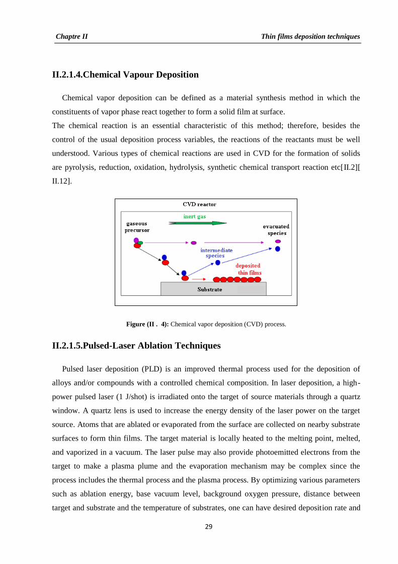
II.2.1.4.Chemical Vapour Deposition
Chemical vapor deposition can be defined as a material synthesis method in which the
constituents of vapor phase react together to form a solid film at surface.
The chemical reaction is an essential characteristic of this method; therefore, besides the
control of the usual deposition process variables, the reactions of the reactants must be well
understood. Various types of chemical reactions are used in CVD for the formation of solids
are pyrolysis, reduction, oxidation, hydrolysis, synthetic chemical transport reaction etc[II.2][
II.12].
Figure (II . 4): Chemical vapor deposition (CVD) process.
II.2.1.5.Pulsed-Laser Ablation Techniques
Pulsed laser deposition (PLD) is an improved thermal process used for the deposition of
alloys and/or compounds with a controlled chemical composition. In laser deposition, a high-
power pulsed laser (1 J/shot) is irradiated onto the target of source materials through a quartz
window. A quartz lens is used to increase the energy density of the laser power on the target
source. Atoms that are ablated or evaporated from the surface are collected on nearby substrate
surfaces to form thin films. The target material is locally heated to the melting point, melted,
and vaporized in a vacuum. The laser pulse may also provide photoemitted electrons from the
target to make a plasma plume and the evaporation mechanism may be complex since the
process includes the thermal process and the plasma process. By optimizing various parameters
such as ablation energy, base vacuum level, background oxygen pressure, distance between
target and substrate and the temperature of substrates, one can have desired deposition rate and

Chaptre II Thin films deposition techniques
30
structural quality. Advantage of PLD technique is direct monitoring of cell-by-cell growth by
reflective high-energy electron diffraction (RHEED) pattern. Major drawbacks of this excellent
technique are the limited area of uniform deposition and particle/particulate ejection from the
target as it was shown in figure(II.5). To avoid the deposition of the microsized ejections, the
substrates are settled at an off-axis position [II.3].
Figure (I . 5) ): Pulsed-Laser Ablation-Based Techniques[II.13].
II.2.1.6.Physical Vapor Deposition (PVD)
PVD processes proceed along the following sequence of steps:
a) The solid material to be deposited is physically converted to vapor phase;
b) The vapor phase is transported across a region of reduced pressure from the source to
the substrate;
c) The vapor condenses on the substrate to form the thin film.
The conversion from solid to vapor phase is done through physical dislodgement of surface
atoms by addition of heat in evaporation deposition or by momentum transfer in sputter
deposition. The third category of PVD technique is the group of so called augmented energy
techniques including ion, plasma or laser assisted depositions. Figure (II . 4) shows the steps of
this operation [II.14].
Chaptre II Thin films deposition techniques
31
Figure(II . 6): Schema of Physical Vapor Deposition (PVD) [ II.15].
II.2.2.Thin film Groth process
Three major steps that constitute a typical thin film deposition process are:
1- production of the appropriate atomic, molecular, or ionic species;
2- transport of these species to the substrate through a medium, in general gases;
3- condensation on the substrate, either directly or via a chemical and/or
electrochemical reaction, to form a solid deposit [II.16].
Figure(II . 7 ): Thin film Groth process [II.17].

Chaptre II Thin films deposition techniques
32
II.2.2.1.Nucleation
The unit species, on impacting the substrate, lose their normal component velocity to the
substrate (provided the incident energy is not too high) and are physically adsorbed on the
substrate surface.
The adsorbed species are not in thermal equilibrium with the substrate initially and move
over the substrate surface. In this process they interact among themselves, forming bigger
clusters. The clusters or the nuclei, as they are called, are thermodynamically unstable and may
tend to desorb in time, depending on the deposition parameters. If the deposition parameters are
such that a cluster collides with other adsorbed species before getting desorbed, it starts
growing in size. After reaching a certain critical size, the cluster becomes thermodynamically
stable and the nucleation barrier is said to have been overcome. This step involving the
formation of stable, chemisorbed, critical-sized nuclei is called the nucleation stage.
II.2.2.2.coalescence
The critical nuclei grow in number as well as in size until a saturation nucleation density is
reached. The nucleation density and the average nucleus size depend on a number of
parameters such as the energy of the impinging species, the rate of impingement, the activation
energies of adsorption, desorption, thermal diffusion, and the temperature, topography, and
chemical nature of the substrate. A nucleus can grow both parallel to the substrate by surface
diffusion of the adsorbed species, and perpendicular to it by direct impingement of the incident
species. In general, however, the rate of lateral growth at this stage is much higher than the
perpendicular growth. The grown nuclei are called islands.
II.2.2.3Growth
The small islands start coalescing with each other in an attempt to reduce the substrate
surface area. This tendency to form bigger islands is termed agglomeration and is enhanced by
increasing the surface mobility of the adsorbed species, for example, by increasing the substrate
temperature. In some cases, formation of new nuclei may occur on areas freshly exposed as a
consequence of coalescence.

Chaptre II Thin films deposition techniques
33
Larger islands grow together, leaving channels and holes of uncovered substrate. The structure
of the films at this stage changes from discontinuous island type to porous network type. Filling
of the channels and holes results in the formation of a completely continuous films [II.18].
Thus statistical process of nucleation, surface-diffusion controlled growth of the three
dimensional nuclei, and formation of a network structure and its subsequent filling to give a
continuous film, these processes constitute the growth process. Growth stages and the initial
nucleation, depends on the thermodynamic parameters of the deposit and the substrate surface,
can be categorized as (a) island type, called Volmer-Weber (VW) type, (b) layer type, called
Frank-Van der Merwe (FV) type, and (c) mixed type, called Stranski-Krastanov (SK) type.
This is shown in Figure (I . 7) [ II.19].
Figure (II . 8): Three modes of thin film growth processes.

Chaptre II Thin films deposition techniques
34
II.3.Conclusion
In this chapter we recalled to the most used techniques to develop deposits of thin films,
especially spray pyrolysis technique we have to prepare our consisted which is illustrated by
more detail in the following chapter.

Chaptre II Thin films deposition techniques
35
References of Chapter II
[II.1] A.R. West,’Solid State Chemistry’ John willey & Sons, Singapore, (2003).
[II.2] K. L. Chopra,’Thin Film Phenomena’, McGraw Hill, New York (1969).
[II.3] S. Menakh, Contribution à l'Etude des Propriétés de Films ZnO, thème de magister,
université de Constantine, 2010.
[II.4] R.R. Chamberline and 1.S. Skarman, 1. Electrochem. Soc., 113 (1966) 86.
[II.5] B .R. Pamplin and S.R. Feigelson, Thin Solid Films, 60 (1979) 14.
[II.6] R . Krishnakumar, Y. Ramaprakash, V. Subramanian, K. Chandrasekhara Pillai and
A.S. Lakshmanan, SPIE Opt. Mater.Tech. Energy Effic., Solar Energy Convers., 562
(1985) 187.
[II.7] C .M. Lampkin, Prog. Cry. Growth Characteristics, 1 (1979) 405.
[II.8] http://spparks.sandia.gov/pictures.html
[II.9] A. Hafdallah, Etude du Dopage des Couches Minces de ZnO Elaborées par Spray
Ultrasonique, thème de magister, université de Constantine, 2007.
[II.10] Y.C. Ke and P. Stroeve, "Polymer-Layered Silicate and Silica Nanocomposites",
Elsevier B.V., oxford, 2005.
[II.11] C.J. Brinker, G.W. Scherer, "Sol Gel Science: The physics and chemistry of sol gel
processing", Academic press inc., Elsevier, 1990.
[II.12] R. P. Sharma, S. V. Patil, S. V. Bhavsar, A. R. Patil, L Dori. Indian J. Pure Appl.
Phys., 37 (1999) 876.
[II.13] I. Guesmi, "Dépôt de couches minces de cuivre sur substrats polymère de formes
complexes par pulvérisation cathodique magnétron avec ionisation de la vapeur",
thèse de doctorat, Université Paris Sud – XI, (2003).
[II.14] Mahan, John E. "Physical Vapor Deposition of Thin Films" John Wiley & Sons
(2000).
[II.15] Mattox, Donald M. "Handbook of Physical Vapor Deposition (PVD) Processing"
Noyes Publications(1998).
[II.16] D.L. Smith, Thin Film Deposition: Principles and Practice, Mc Graw Hill, New York
(1995).
[II.17] http://www.pob.manchester.ac.uk/research.html
[II.18] www.cefi.org/fraDESS.old/dess_265.html

Chaptre II Thin films deposition techniques
36
[II.19] M. Guth, "Propriétés de transport de jonction tunnels magnétique utilisant un
composé II-VI de ZnS Comme barrière tunnel", thèse de doctorat, Université Louis
Pasteur de Strasbourg, (2003).
Chapter III
Preparation and Characterization
of Zinc Oxide.
Chapter III Preparation and Characterization of Zinc Oxide
38
III.Preparation and Characterization of Zinc Oxide
This chapter will describe the filing system used in this work which is in the spray
pyrolysis case for the development of thin film are ZnO and the used characterization
techniques address to track and measure the various properties of these thin layers developed
by this technique.
III.1.Spray pyrolysis deposition system
III.1.1.Installation of experiential
The experimental setup used in the laboratory (VTRS): Valorisation et Technologie des
Resources Sahariennes for the preparation of ZnO and ZnO:La thin films is shown in Fig(III.
1).
Figure (III . 1): Photo for spray pyrolysis home made.

Chapter III Preparation and Characterization of Zinc Oxide
39
System components:
Number System components
1 Solution reservoir and Atomizer
2 Air compressor
3 Nozzle
4 Substrate holder
5 Temperature controller
6 Moving nozzle
7 Spray pyrolysis home made
III.1.2.Role of the mounting elements
The main elements are:
1. A substrate holder: it is a 08cm diameter plate heated by the Joule effect, the
temperature can be controlled using a temperature controller which is connected to a
thermocouple type K.
2. Solution reservoir: it feeds, low flow, atomizer (the nozle).
3. Air compressor: That converts the solution at the atomizer in a jet of very fine
droplets of 40 µm.
III.2.4.1 Experimental conditions in ZnO thin films
In our work, a number of parameters were varied to study the deposition of ZnO thin films,
these experimental parameters are:
The substrate temperature 375 ° C.
the solution used, we used zinc acetate as the zinc source.
The fixed parameters are:
The molarity of the solution to 0.5M zinc acetate obtained when dissolving (2.1951 g
(Zn (CH3COO)2, 2H2O) in 20 ml (1:1 methanol bidistilled water).
Deposit Time Scanning 37sec.
The amount of solution: 20 ml.
Chapter III Preparation and Characterization of Zinc Oxide
40
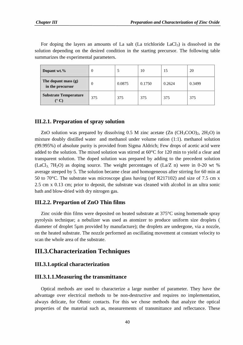
For doping the layers an amounts of La salt (La trichloride LaCl3) is dissolved in the
solution depending on the desired condition in the starting precursor. The following table
summarizes the experimental parameters.
Dopant wt.% 0 5 10 15 20
The dopant mass (g)
in the precursor 0 0.0875 0.1750 0.2624 0.3499
Substrate Temperature
(° C) 375 375 375 375 375
III.2.1. Preparation of spray solution
ZnO solution was prepared by dissolving 0.5 M zinc acetate (Zn (CH3COO)2, 2H2O) in
mixture doubly distilled water and methanol under volume ration (1:1). methanol solution
(99.995%) of absolute purity is provided from Sigma Aldrich; Few drops of acetic acid were
added to the solution. The mixed solution was stirred at 60°C for 120 min to yield a clear and
transparent solution. The doped solution was prepared by adding to the precedent solution
(LaCl3, 7H2O) as doping source. The weight percentages of (La/Z n) were in 0-20 wt %
average steeped by 5. The solution became clear and homogeneous after stirring for 60 min at
50 to 70°C. The substrate was microscope glass having (ref R217102) and size of 7.5 cm x
2.5 cm x 0.13 cm; prior to deposit, the substrate was cleaned with alcohol in an ultra sonic
bath and blow-dried with dry nitrogen gas.
III.2.2. Prepartion of ZnO Thin films
Zinc oxide thin films were deposited on heated substrate at 375°C using homemade spray
pyrolysis technique; a nebulizer was used as atomizer to produce uniform size droplets (
diameter of droplet 5µm provided by manufacture); the droplets are undergone, via a nozzle,
on the heated substrate. The nozzle performed an oscillating movement at constant velocity to
scan the whole area of the substrate.
III.3.Characterization Techniques
III.3.1.optical characterization
III.3.1.1.Measuring the transmittance
Optical methods are used to characterize a large number of parameter. They have the
advantage over electrical methods to be non-destructive and requires no implementation,
always delicate, for Ohmic contacts. For this we chose methods that analyze the optical
properties of the material such as, measurements of transmittance and reflectance. These

Chapter III Preparation and Characterization of Zinc Oxide
41
spectroscopic measurements is to determine the optical refractive index, the thickness of the
material and the optical gap. Devices that are been available Shmatzu 1800 VTRS laboratory.
III.3.1.2.UV-Visible Spectrometer
UV-Visible Spectrometer is used for measuring the optical transparency of thin films and
chemical solutions in the UV-visible range. A beam of light in the UV-Vis-NIR range from a
lamp is allowed to interact with the specimen. The optical properties such as the optical band
gap and refractive index of the specimen are measured by utilizing absorption, transmission,
and reflection data as function of wavelength of the incident light [III.1]. whose operating
principle is shown in (Figure III.1).
Figure (III . 2) : shows the spectral analysis of UV–Visible.
We were able to draw curves representing the variation of the transmittance versus the
wavelength in the field of UV-visible ranging (200-900nm). By exploiting these curves it is
possible to calculate thickness of the films, and optical characteristics: the optical absorption
threshold, the absorption coefficient, the band gap and refractive index.
III.3.1.3.The spectra of transmittance
The transmittance T, is defined as the ratio of transmitted light intensity to incident light
intensity [III.2]. For the transmittance curves, our ZnO thin films were deposited on glass.
This is necessary because it does not absorb light in the spectral range (200-900nm). A
substrate (ref R217102) blank in the spectrophotometer of the reference beam was used for
plotting spectra, a computer connected to this unit reproduces the spectra representing the
transmittance depending on the wavelength of the incident beam. An example of these spectra
is shown in (Figure III.3), where we distinguish two areas:
Chapter III Preparation and Characterization of Zinc Oxide
42
a. A field spanning wavelengths (400-900nm) where the transmittance has a series of
interference fringes due to multiple reflections in the ZnO thin films. This area will allow
us to determine the thickness of thin films and the refractive index.
b. The second area where the transmittance begins to decrease rapidly (≤400nm) we used
for determining the optical absorption threshold.
Figure( III . 3): transmittance spectra of nudoped ZnO on the wavelength (from our Works).
III.3.1.4. The spectra of absorption
Transmission is related to absorption coefficient () and film thickness (d) as shown in
Equation (III.1) [ III.3]:
( ) ( )
The absorption coefficient () was calculated from the expression.
(
) ( )
Where: d is thickness of the film and T is optical transmission [III.4].
By plotting (αhυ)2 against hυ, the band gap value can be extrapolated from the straight line
at (αhυ)2 = 0. The obtained value of the undoped ZnO band gap, from this work, is Eg ≈ 3.27
eV .

Chapter III Preparation and Characterization of Zinc Oxide
43
Fig (III . 2) : shows the ZnO band gap.
III.3.1.5.Urbach Energy
The optical transitions between occupied states in the valence band tail to unoccupied
states of the conduction band edge induce an exponential dependence of the absorption
coefficient a on photon energy near the band edge [III.5]. To describe this phenomenon, the
Urbach energy EU is introduced. EU refers to the width of the exponential absorption edge
deduced from inverse of the slope of the curve ln() as a function of hυ, described by:
(
) ( )
( )
where a0 is a constant [III.6].
III.3.2. Thickness of deposited thin films
We used the program Hebal Optic on computer to calculate the thickness of thin films,
which provides us with the amount of the thickness directly.
III.3.3. Structural characterization of thin films of ZnO
This study is performed by X-ray diffraction, which provides information on the crystal
structure and the most important structural characteristics.

Chapter III Preparation and Characterization of Zinc Oxide
44
III.3.3.1. X-Ray Diffraction (XRD)
XRD is a precise and popular method for determining the crystal structures of thin films
and it is essentially non-destructive. It gives information about the crystal structure,
orientations, lattice constants, crystallite size and composition with the help of Joint
Committee on Powder Diffraction Standards(JCPDS) of the sample. Analysis of the
diffraction pattern obtained, by comparing with the standard JCPDS data can reveal the
existence of different crystallographic phases in the film, their relative abundance and
preferred orientations. From the width of the diffraction line the average grain size of the film
can also be estimated.
III.3.3.2.Principle
When a monochromatic X-ray beam is directed onto a polycrystalline material, it is partly
reflected by the atomic planes of certain crystals. For the diffraction of X photons is
measured, the incidence of the beam relative to the atomic planes to take place at a particular
angle. As illustrated in figure(III.3), It is necessary that the reflected waves are in phase so to
interfere constructively and to be measured by the detector.
Figure( III . 3) : shows the x-ray diffraction.
The interlinear spacing dhkl can be calculated from the X-ray diffraction profiles using the
well known formula:
( )
Where: dhkl is interplanar spacing, θ is the Bragg angle, n is the order of the reflection, λ
is the wavelength of X-rays [III.7].
The diffractogram is a recording of the diffracted intensity versus the 2θ angle formed with
the direct beam. The study of the diffraction pattern can be traced back to a lot of information
Chapter III Preparation and Characterization of Zinc Oxide
45
on structural and microstructural sample such as crystal structures, crystallite size, rates of
structural defects, macro and micro stress and presence a texture. The angular positions of the
diffraction lines are characteristic parameters of the crystal lattice. The study of diffraction
line positions thus can be traced back to the crystal lattice of each sample of the crystallized
phases. Once the network determined, the angular positions of the lines used to calculate the
inter reticular distances (d) of diffracting atomic planes and thus access to cell parameters for
example ZnO:
(
)
( )
Where: α, c are the lattice parameters, hkl are the Miller indices of the planes, and dhkl is the
interplanar spacing [III.8].
Positions and intensities of the diffraction lines of most known materials have been
investigated and are listed in databases. The comparison with an experimental diffraction data
allows to find the nature of each component phase of the sample. As part of our study, were
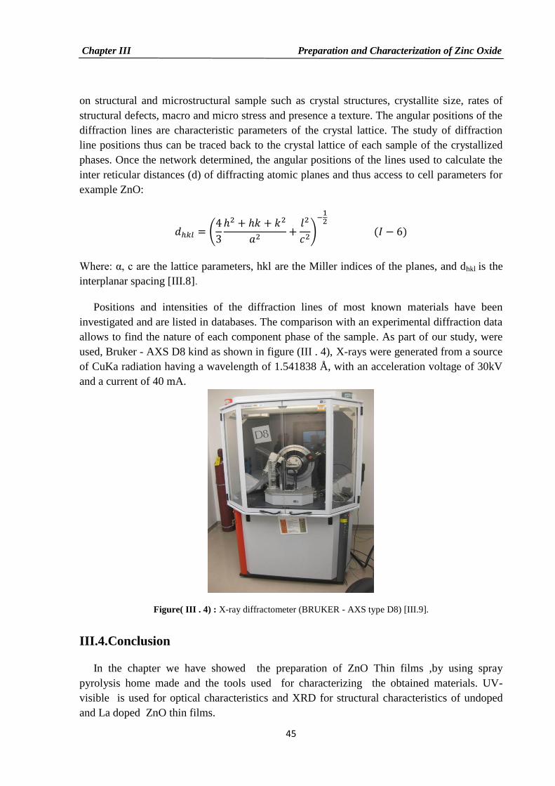
used, Bruker - AXS D8 kind as shown in figure (III . 4), X-rays were generated from a source
of CuKa radiation having a wavelength of 1.541838 Å, with an acceleration voltage of 30kV
and a current of 40 mA.
Figure( III . 4) : X-ray diffractometer (BRUKER - AXS type D8) [III.9].
III.4.Conclusion
In the chapter we have showed the preparation of ZnO Thin films ,by using spray
pyrolysis home made and the tools used for characterizing the obtained materials. UV-
visible is used for optical characteristics and XRD for structural characteristics of undoped
and La doped ZnO thin films.

Chapter III Preparation and Characterization of Zinc Oxide
46
References of Chapter III
[III.1] H. V. GARCIA, M. H. VéLEZ, O. S. GARRIDO, J.M MARTINEZ, J. JIMéNEZ,
“CdS doped-MOR type zeolite characterization, Solid State Electronics”, Vol 43,
p1171-1175, (1999).
[III.2] Jurgen R. Meyer-Arendt,'Introduction to classical and Mdern optics', Fourth Edition,
published by Prentice-Hall, Inc (1995).
[III.3] Gillispie, Meagen Anne, "Metal oxide-based transparent conducting oxides " (2006).
Retrospective Theses and Dissertations. Paper 1891.
[III.4] R.D. Tarey and T.A. Raju, “A method for the deposition of transparent conducting
thin films of Tin Oxide," Thin Solid Films, 128, 181-189, (1985).
[III.5] F.Z. Bedia , A. Bedia , N. Maloufi, M. Aillerie, F. Genty, B. Benyoucef , ''Effect of
tin doping on optical properties of nanostructured ZnO thin films grown by spray
pyrolysis technique'', Journal of Alloys and Compounds 616 (2014) 312–318.
[III.6] F. Urbach, Phys. Rev. 92 (1953) 1324.
[III.7] B .D. Cullity, Elements of X-ray Diffraction, Addison-Wesley Publishing Company,
Inc., Massachusetts (1967).
[III.8] Y. Morinaga, K.Sakuragi, N.Fujimura, T.Ito, Effect of Cedoping on the growth of
ZnO thin films, J.Cryst.Growth174(1997)691–695.
[III.9] http://www.go-dove.com/en/auction/view?id=8629317
Chapter IV
Results and Discussion

Chapter IV Results and Discussion
48
IV. Result and Discussion
In this chapter we present the results of our work on the preparation and characterization of
thin films of zinc oxide (ZnO) undoped and La doped deposited by spray pyrolysis technique.
The influence of doping to the different structural, optical and properties was studied. The
films obtained were characterized by various techniques. The XRD to study the structure, the
lattice constant a ,c the grain size. The optical transmission in the UV-visible for the
determination of the fundamental optical properties, namely, the optical gap, Urbach energy,
the thickness of thin films and refractive index. Note that these different characterization
methods have been developed in chapter III.
IV.1.structural properties
IV.1.1. X-Ray Diffraction
The X-ray diffraction patterns of undoped and La doped ZnO thin films are presented in
Figure (IV.1) Here the diffraction peaks observed at 2θ = 31.8°, 34.5°, 36.4°, 56.76° and
62.89° are indicted with following plans (100), (002), (101), (110) and (103) respectively. All
the diffraction peaks correspond to hexagonal wurtzite phase in agreement with the respective
Joint Committee on Powder Diffraction Standards (JCPDS) card no. 36-1451, with the space
group P63mc (186) [IV.1].
It is worth noting that no additional peaks within the XRD detection limits due to other
oxide phases are present for all the prepared thin films in the XRD pattern, indicating the
phase purity of ZnO thin films prepared by this method and revealing that La3+
ion (1.15 Å)
might substitute Zn2+
ion (0.74 Å) or incorporate into interstitial sites in the ZnO lattice.
Moreover, (002) diffraction peak for the ZnO films, except 5wt. % La doping, is the highest
one. This indicate that the undoped and 10-20wt. % film have preferential c-axis orientation.
Chapter IV Results and Discussion
49
Figure (IV. 1): The X-ray diffraction patterns of undoped and La doped ZnO thin films between (0wt.% and
20wt.%).
Whereas for 5 wt. % La doping ZnO, diffraction peak at [100] as preferred orientation and
two peaks having comparative intensities such as (002) and (101), were observed from these
spectra, leading to an increase in growth crystallite size as it will be detailed in the following
section. A part of 5wt. % La doped thin film one can observe that the film doped at 15 wt. %
has higher and sharper diffraction peak along (002) direction indicating an improvement in
this peak intensity compared to the undoped ZnO thin film and others La doped films (10 and
20wt.% level doping) This film exhibits nanoycrystalline structure and having hexagonal
wurtzite structure with (002) orientation. The high of intensity along (002) direction maybe
due to the level doping and degree of substitution of Zn2+
ions by La3+
ions. This result
indicates that the doping level of the films improved the structure properties.
It means the ZnO lattice is expended along the c-axis and the La+ ions substitute Zn
+ ions into
ZnO lattice [IV.2] for those amount of doping.
IV.1.2. Determining The lattice parameters a ,c
The lattice constant a ,c for ZnO thin films can be calculated by using the following equation :
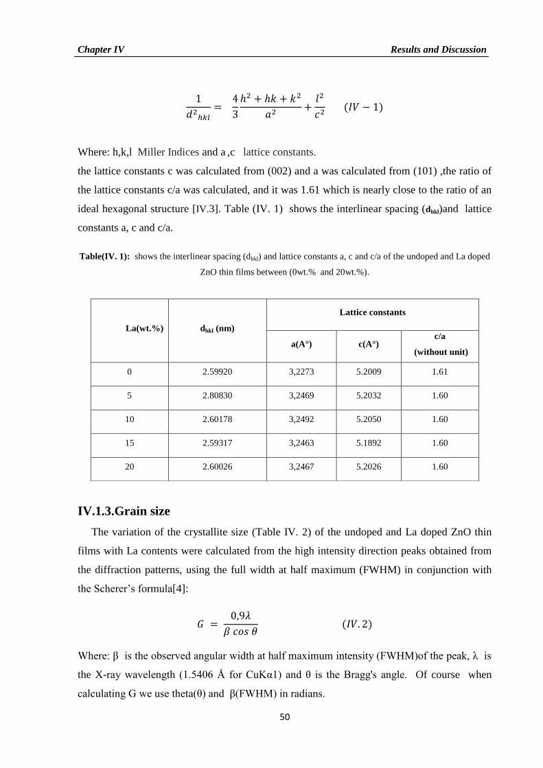
Chapter IV Results and Discussion
50
Where: h,k,l Miller Indices and a ,c lattice constants.
the lattice constants c was calculated from (002) and a was calculated from (101) ,the ratio of
the lattice constants c/a was calculated, and it was 1.61 which is nearly close to the ratio of an
ideal hexagonal structure [IV.3]. Table (IV. 1) shows the interlinear spacing (dhkl)and lattice
constants a, c and c/a.
Table(IV. 1): shows the interlinear spacing (dhkl) and lattice constants a, c and c/a of the undoped and La doped
ZnO thin films between (0wt.% and 20wt.%).
IV.1.3.Grain size
The variation of the crystallite size (Table IV. 2) of the undoped and La doped ZnO thin
films with La contents were calculated from the high intensity direction peaks obtained from
the diffraction patterns, using the full width at half maximum (FWHM) in conjunction with
the Scherer’s formula[4]:
Where: β is the observed angular width at half maximum intensity (FWHM)of the peak, λ is
the X-ray wavelength (1.5406 Å for CuKα1) and θ is the Bragg's angle. Of course when
calculating G we use theta(θ) and β(FWHM) in radians.
La(wt.%) dhkl (nm)
Lattice constants
a(A°) c(A°) c/a
(without unit)
0 2.59920 3,2273 5.2009 1.61
5 2.80830 3,2469 5.2032 1.60
10 2.60178 3,2492 5.2050 1.60
15 2.59317 3,2463 5.1892 1.60
20 2.60026 3,2467 5.2026 1.60

Chapter IV Results and Discussion
51
Table(IV. 2): shows the crystallite size of the undoped and La doped ZnO thin films between (0wt.% and
20wt.%).
IV.3.Optical Properties
IV. 3.1. Effect of the concentration of dopant on the spectra transmittance of ZnO
thin films
Figure (IV. 2) shows the optical transmission as a function of the wavelength in 200-
900nm range of undoped and La doped ZnO thin films with doping level. As can be seen, a
region of strong transparency is located between 380-900nm. In the visible region the value of
the average transmission is over than 85% and we remarked that the effect of doping is to
reduce transmittance due to energy loss caused by free electrons generated by La doping. A
drastic deacreas in trasnmition is located between 360-380nm reveling the region of the
absorption edge in the layers due to the transition between the valence band and the
conduction band in this region the transmission decreases because of the onset fundamental
absorption.
In the region lower than 360nm, we are noting that the doping effect is clearly observed in
the layer quality; as can be seen from figure(IV. 2) the transmittance spectra evoke a
considerable large peak in this region when the La doping level becomes equal to 15wt. %
which is maybe due to existence of pourers region letting the passage of light through it hence
the particles size reach its minimum value with the case of this doping level. This behavior is
attuned when the La doping level reach 20wt. % and peak become less pronounced as it seen
in insert of figure (IV. 2) which may be due to the crystallite size increasing as illustrated in
table (IV. 1) above.
dopant wt.% 2θ(°2Theta) FWHM (°2Th) G (Crystallite size)
(nm)
0 34.5076 0.2342 41,45
5 31.8670 0.2007 62,17
10 34.4724 0.2007 55,23
15 34.5904 0.2007 20,72
20 34.4932 0.2007 49,72

Chapter IV Results and Discussion
52
Figure(IV. 2): shows the spectra optical transmission of undoped and La doped ZnO thin films between
(0wt.% and 20wt.%).
IV.3.2.Optical gap of variation depending on the concentration of
Lanthanum (La)
The band gap of the ZnO thin films deposited on glass substrate and prepared by spray
porolysis was determined from the transmission spectra by means of a graphic method based
on the variation of the absorption coefficient (αhν)2 depending hυ (Figure IV. 3).
Figure (IV. 3): shows the optical band gap for pure and doped ZnO thin films.

Chapter IV Results and Discussion
53
Band gap energy Eg values, deduced from figure(IV. 3) are illustrated in Table (IV. 3).
Table(IV. 3):The band gape of pure and doped ZnO thin films.
Dopant(wt%) Eg (eV)
0 3.286
5 3.293
10 3.300
15 3.320
20 3.310
IV. 3.3. Change in energy Urbach (EUrb) depending of doping
The inset shows the drawn of ln A as a function of photon energy (hν) for Urbach energy
deducing. As clearly seen in Figure (IV. 3), the optical gap energy reveal slight increase with
increasing of La doping from 0 to 15 wt. % then decreases for 20wt. % La doping level. The
obtained values of band gap are listed in Table (IV. 3). It was found that the Eg value for all
the samples is over than that of the Eg value for pure ZnO (3.28 eV). This might be due to
lower defect concentration in the crystals of La doped ZnO or due to Burstein-Moss band-
filling effect, which causes the energy band widen (blue-shift) since Urbach energy remains
practically constant with increasing the band gap indicating the independence of band gap on
defects.
It is worth noting that a minimum of Urbach energy was reached with 15 wt. % La doping
ZnO thin films, which means that the doping has less disorder in the film network. Such less
disorder reveal the good crystallinity of the thin films as it was correlated to the results carried
out by DRX investigations in the above section.
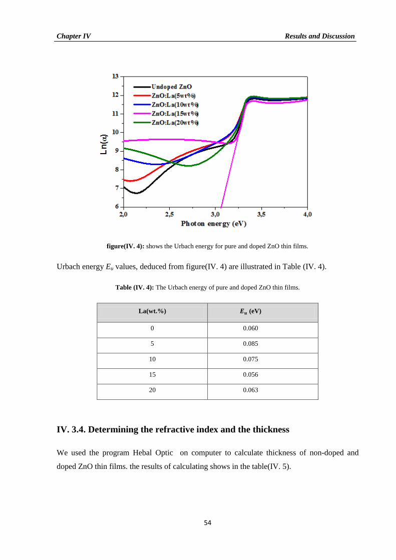
Chapter IV Results and Discussion
54
figure(IV. 4): shows the Urbach energy for pure and doped ZnO thin films.
Urbach energy Eu values, deduced from figure(IV. 4) are illustrated in Table (IV. 4).
Table (IV. 4): The Urbach energy of pure and doped ZnO thin films.
La(wt.%) (eV)
0 0.060
5 0.085
10 0.075
15 0.056
20 0.063
IV. 3.4. Determining the refractive index and the thickness
We used the program Hebal Optic on computer to calculate thickness of non-doped and
doped ZnO thin films. the results of calculating shows in the table(IV. 5).

Chapter IV Results and Discussion
55
Table(IV. 5): Refractive index and thickness doped ZnO (0-20w%).
Dopant(wt.%) thickness (nm) refractive index
0 174 1.824
5 184 1.66
10 156 1.71
15 111 1.70
20 130 1.75
IV.4. Electrical Properties
The electrical properties of interest are the type of carriers, resistivity, mobility and carrier
concentration. Here we describe the commonly used parameters. For the electrical properties
of our elaborated ZnO thin films, due to its high resistivity we have difficulties to carry out
result.
IV.5.Conclusion
Undoped and La doped ZnO thin films are successfully prepared using inexpensive spray
pyrolysis technique with moving nozzle. Structural and optical properties, of elaborated
undoped and La-doped ZnO thin films, were investigated. XRD study indicated that the films
are polycrystalline nature and hexagonal wurtzite structure. La-doped ZnO thin films, except
5wt. % La-doped one, have [002] as preferred orientation whereas 5wt. % La-doped ZnO has
tow preferred orientations with (002) one and its peaks exhibited a sleigh shift toward lower
angles proving Zn+ substitution by La
+ ion when compared with undoped ZnO one. The
maximum average cryristalite size was 62nm for 5wt. % La doped ZnO. The average
transparency in the visible range was found around 90% and the absorption edge sifted to
lower wavelength when La dopant was increased to 15wt. % then return; the energy band gap
of La-doped thin films, depending slightly on La doping level, varied in a range of 3.29-
3.32eV. It was found that the disorder of defects in structure surveyed by deduction of Urbuch
energy did not affected the energy band gap. confinement in the films and were well
correlated to the less disorder in the film network deduced by Urbuch energy.

Chapter IV Results and Discussion
56
References of Chapter IV
[IV.1] S. Benramache, B. Benhaoua, F. Chabane, F.Z. Lemadi, J. Semiconduct. 34 (2013).
023001-4.
[IV.2] S. Benramache, B. Benhaoua, F. Chabane, Effect of substrate temperature on
thestability of transparent conducting cobalt doped ZnO thin films, J.
Semiconduct.33 (2012) 093001–93011.
[IV.3] K. Kim, et al., “Realization of p-Type ZnO Thin Films,” Applied Physics Letters,
Vol. 83, No. 1, 2003, pp. 63-65. doi: 10.1063/1.1591064.
[IV.4] S. Rani, P. Suri, P.K. Shishodia, R.M. Mehra, Synthesis of nanocrystalline
ZnOpowder via sol–gel route for dye-sensitized solar cells, Sol. Energy Mater.
Sol.Cells 92 (2008) 1639–1645.

Conclusion
Conclusion
Conclusion
The objectives set in, the context of this work, consists in the development of transparent
conductive glasses in the form of thin films from metal oxide which is ZnO. The development
of thin films of these TCO by the technique of spray pyrolysis, had been reached.
Structural characterizations are carried out by using XRD diffractometer (BRUKER - AXS
type D8) equipped with X’Pert High Score under Cu Kα (λ = 1.54056Å) radiation. For optical
transmission spectra we have used an UV-visible spectrophotometer (Shimadzu, Model 1800)
in spectral region 200-900 nm. The film thickness was estimated from the exhibited
interference patterns of the transmission spectra.
Undoped and La doped ZnO thin films are successfully prepared using inexpensive spray
pyrolysis technique with moving nozzle structural and optical properties, of elaborated
undoped and La-doped ZnO thin films, were investigated. DRX study indicated that the films
are polycrystalline nature and hexagonal wurtzite structure. La-doped ZnO thin films, except
5wt.% La-doped one, have (002) as preferred orientation whereas 5wt.% La-doped ZnO has
tow preferred orientation with (002) one and its peaks exhibited a sleigh shift toward lower
angles proving Zn+ substitution by La
+ ion when compared with undoped ZnO one the
maximum average cryristalite size was 62 nm for 5wt.% La-doped ZnO. The average
transparency in the visible range was found around 90% and the absorption edge sifted to
lower wavelength when La dopant was increased to 15wt.% then return. Eg of La doped thin
films, depending slightly on La doping level and varied in the range 3.29-3.32eV. It was
found that the disorder of defects in structure surveyed by deduction of Urbuch energy did not
affected the energy band gap.
We advice in the future to study the electric properties and annealing temperature on its
properties. Also the effect of co-doped ZnO.

Abstract
Zinc oxide (ZnO) is a Transparent Conductive Oxides TCO material with interesting
physical properties, which places it among the most promising materials for use in various
fields such as piezoelectricity, photovoltaic effect, optoelectronics...etc.
In this work, we have prepared, undoped and La doped ZnO thin films, between (0wt.%
and 20wt.%) LaCl3 was used as source of dopant in the precursor of Zn+2
which was
obtained by dissolving Acetate Zinc in 1:1 methanol-double distilled water, on heated glass
substrates (375 °C) by spray pyrolysis technique in our laboratory named VTRS ( laboratoire
de valorisation et technologie des ressources sahariennes). A fundamental study of their
Structural and opto-electrical properties such as crystallization, optical transmittance spectra,
energy gap and grain size of these materials. These properties of the obtained thin films were
characterized by (XRD and UV-visibele).
X-ray diffraction analysis showed that all the films are polycrystalline with a hexagonal
wurtzite structure and a preferred orientation along the (002) plane. and having crystallite size
average (20 – 62) nm.
Spectrophotometric measurements in UV-visible range have showed that all the films have
a high transmission of about 90% in the visible zone with a band gap energy ranged in (3.28 -
3.3) eV.
It was found that the disorder of defects in the structure surveyed by deducting the Urbuch
energy did not affect the energy band gap, indicating the reliability of this method (spray
pyrolysis home made).
Keywords: Transparent Conductive Oxides(TCO), spray pyrolysis, zinc oxide, thin films.

Résumé
L'oxyde de zinc (ZnO) est un matériau de la famille des Oxydes Transparent Conducteurs
(TCOs) avec des propriétés physiques intéressantes. Ce matériau est prometteur pour
l'utilisation dans divers domaines tels que la piézoélectricité, effet photovoltaïque, de
l'optoélectronique ...etc.
Dans ce travail, nous avons préparé des couche minces de ZnO, non dopé et dopé La
entre(0% et 20% en poids La/Zn), LaCl3 a été utilisé comme source de dopant dans le
précurseur de Zn+ 2
, qui a été obtenue par dissolution de l'acétate de zinc en 1:1 méthanol l'eau
bidistillée. Ce matériau est déposé sur des substrats de verre chauffés (375 °C) par
pulvérisation pyrolyse au sein de l'unité Matériaux solaires et application du laboratoire de
valorisation et technologie des ressources sahariennes (VTRS). Une étude fondamentale des
propriétés structurelles et opto-electriques telles que la cristallisation et la taille de grain de
ces matériau, les spectres de transmittance et la gap optique. Ces propriétés des couches
minces obtenus ont été caractérisés par (XRD and UV-visibele).
L'analyse par diffraction des rayons X a montré que tous les films sont polycristallin avec
une structure de wurtzite hexagonale et une orientation préférentielle le long du plan (002), et
ayant des cristallites de taille moyenne de l'ordre de (20 à 62) nm.
Les mesures spectrophotométriques dans la gamme UV-visible ont montré que tous les films
ont une transmission élevée d'environ 90% dans la zone visible avec une énergie de bande
interdite se trouvant dans la gamme (3.28 au 3.3) eV.
Il a été constaté que le trouble de défauts dans la structure interrogés par déduction de
l'énergie d'Urbuch n'a pas affecté l'écart de bande d'énergie et indiquant la fiabilité de ce
méthode (spray pyrolyse home made).
Mots-clés: Oxydes Conducteurs Transparents(OCT), spray pyrolyse, Oxyde de zinc, Couche
mince.

ملخص
خصائص فيزيائية هامةمع (TCO) االكاسيد الشفافة الناقلة مواد عائلة من ( هوZnOأكسيد الزنك )
وتأثير الضوئية :وهو ما يجعلها من بين أكثر المواد الواعدة الستخدامها في مختلف المجاالت مثل
. واإللكترونيات الضوئية ... الخ
- %. wt 0) بيناألغشية الرقيقة ألكسيد الزنك النقي والمطعم باللنتموان في هذا العمل، قمنا بإعداد
00 wt .% )) ستخدمن LaCl3 التي تم الحصول عليها عن طريق إذابة خالت )كمصدر لإلشابة الزنك
تقنية عن طريق ) C 573°) حتى خنةمسالزجاج على ركائز الماء المقطرو الميثانول من1: 1الزنك في
األساسية مثل الخصائص الفيزيوكيميائية دراسة ل. (VTRS)الحراري في مختبرنا الكيميائي الرش
.هذه الموادل البصرية، فجوة الطاقة وحجم الحبيبات التبلور، أطياف النفاذية
ألفالم التي تم الحصول عليها من خالل تقنيات لالبصرية والكهربائية يزت الخصائص الهيكلية، وتم
والتوجه wurtzite سداسي هيكل تتبلورفيوأظهر تحليل حيود األشعة السينية أن جميع األفالم .مختلفة
.( نانومتر20-00)ما بين الحبيبات حجم متوسط و (.000البلوري)المتجه المفضل هو
٪ في 00وقد أظهرت قياسات طيفية في نطاق األشعة فوق البنفسجية أن كل األفالم لديها انتقال عالية
.( فولت5،5 - 5،02) يتراوح فاصل طاقيمع االشعة المرئية منطقة
.(الحراريالرش الكيميائي ) هذه الطريقة مصداقية، مما يدل على ثابتة Urbuch طاقة ان تبين
األكاسيد الشفافة الناقلة، الرش الكيميائي الحراري، أكسيد الزنك، الطبقات الرقيقة.الكلمات المفتاحية: