Embed Size (px)
Citation preview

RESEARCH
Structural and morphological properties of ITO thin films grownby magnetron sputtering
Z. Ghorannevis1 • E. Akbarnejad2 • M. Ghoranneviss2
Received: 8 June 2015 / Accepted: 15 August 2015 / Published online: 7 October 2015
� The Author(s) 2015. This article is published with open access at Springerlink.com
Abstract Physical properties of transparent and con-
ducting indium tin oxide (ITO) thin films grown by
radiofrequency (RF) magnetron sputtering are studied
systematically by changing deposition time. The X-ray
diffraction (XRD) data indicate polycrystalline thin films
with grain orientations predominantly along the (2 2 2) and
(4 0 0) directions. From atomic force microscopy (AFM) it
is found that by increasing the deposition time, the
roughness of the film increases. Scanning electron micro-
scopy (SEM) images show a network of a high-porosity
interconnected nanoparticles, which approximately have a
pore size ranging between 20 and 30 nm. Optical mea-
surements suggest an average transmission of 80 % for the
ITO films. Sheet resistances are investigated using four-
point probes, which imply that by increasing the film
thickness the resistivities of the films decrease to
2.43 9 10-5 X cm.
Keywords Indium tin oxide � Magnetron sputtering �Thickness
Introduction
Transparent conducting oxide (TCO) thin films are used for
various optoelectronics applications such as plasma dis-
plays, solar cells, and organic light-emitting diodes. TCO
thin films are grown with different materials such as zinc
oxide, tin oxide, indium tin oxide and cadmium tin oxide,
as they possess unique electrical and optical properties
including good conductivity (about 104 X-1 cm-1) and
high transmittance (85 %) in the visible region due to its
large band gap of about 3.70 eV [1, 2]. In2O3:Sn (also
called indium tin oxide or ITO) is a well-known TCO. As-
grown ITO films are usually highly degenerate n-type
semiconductors due to their large number of oxygen
vacancies as well as substitution Sn dopants [3–5].
The physical properties of ITO films such as microstruc-
ture, electrical and optical properties depend on the deposition
methods and experimental conditions. Various growth con-
ditions may affect the crystalline, impurity levels and surface
roughness as well as the band gap of the grown thin films [3,
6].Various techniques, such as electron beamevaporation [7],
ion beam-assisted deposition [8], pulsed laser ablation [9, 10],
ion implantation [11] and RF/DC magnetron sputtering [12–
14], are applied for deposition of ITO thin films. Besides the
process parameters, the thickness also can affect the proper-
ties of the samples [15–22].
In this study, we report the physical properties of ITO
thin films prepared via RF sputtering. The sputtering sys-
tem used in these experiments is a homemade setup and
can simultaneously accommodate up to four targets, which
makes it an ideal setup for developing thin-film solar cells,
without breaking the high vacuum. The substrates can be
rotated to be placed under the next target and different
layers can be deposited in a high vacuum one by one. The
effects of film thickness on the properties of the ITO films
were studied to obtain the optimum growth condition to
fabricate CdTe/CdS thin-film solar cells. Still, it is a
challenge to find an optimum condition to improve both
optical and electrical properties which are the fundamental
aspects for TCO layers.
& Z. Ghorannevis
1 Department of Physics, Karaj Branch, Islamic Azad
University, Karaj, Iran
2 Plasma Physics Research Centre, Science and Research
Branch, Islamic Azad University, Tehran, Iran
123
J Theor Appl Phys (2015) 9:285–290
DOI 10.1007/s40094-015-0187-3
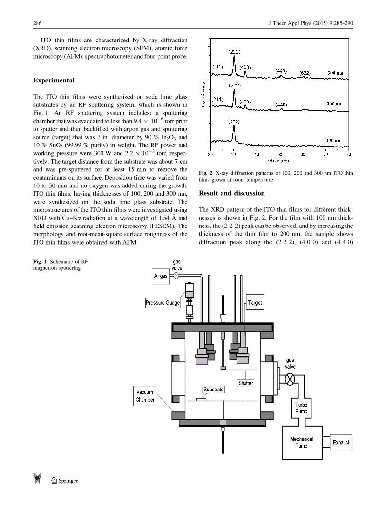
ITO thin films are characterized by X-ray diffraction
(XRD), scanning electron microscopy (SEM), atomic force
microscopy (AFM), spectrophotometer and four-point probe.
Experimental
The ITO thin films were synthesized on soda lime glass
substrates by an RF sputtering system, which is shown in
Fig. 1. An RF sputtering system includes: a sputtering
chamber that was evacuated to less than 9.4 9 10-6 torr prior
to sputter and then backfilled with argon gas and sputtering
source (target) that was 3 in. diameter by 90 % In2O3 and
10 % SnO2 (99.99 % purity) in weight. The RF power and
working pressure were 300 W and 2.2 9 10-2 torr, respec-
tively. The target distance from the substrate was about 7 cm
and was pre-sputtered for at least 15 min to remove the
contaminants on its surface. Deposition time was varied from
10 to 30 min and no oxygen was added during the growth.
ITO thin films, having thicknesses of 100, 200 and 300 nm,
were synthesized on the soda lime glass substrate. The
microstructures of the ITO thin films were investigated using
XRD with Cu–Ka radiation at a wavelength of 1.54 A and
field emission scanning electron microscopy (FESEM). The
morphology and root-mean-square surface roughness of the
ITO thin films were obtained with AFM.
Result and discussion
The XRD pattern of the ITO thin films for different thick-
nesses is shown in Fig. 2. For the film with 100 nm thick-
ness, the (2 2 2) peak can be observed, and by increasing the
thickness of the thin film to 200 nm, the sample shows
diffraction peak along the (2 2 2), (4 0 0) and (4 4 0)
Fig. 1 Schematic of RF
magnetron sputtering
Fig. 2 X-ray diffraction patterns of 100, 200 and 300 nm ITO thin
films grown at room temperature
286 J Theor Appl Phys (2015) 9:285–290
123
directions, where the (2 2 2) peak has the preferred orien-
tation (maximum intensity). Furthermore, by increasing the
thickness to 300 nm, additional diffraction peaks also
appear, such as the formation of crystallites in the (2 1 1),
(2 2 2), (4 0 0), (4 4 0) and (6 2 2) orientations with a
preferred orientation still along the (2 2 2) direction. These
data are in good agreement with the reported values [21].
The peak is verified to be the (2 2 2) peak of cubic bixbyite
In2O3. On the whole, we could report that a crystalline
structure is observed for ITO film grown on glass prepared
by RF magnetron sputtering at room temperature even when
the thickness is 100 nm. In fact, it is quite possible to acquire
a crystalline structure even for the ITO film deposited at
room temperature, if only the thickness is large enough.
These results can help in the growth of TCO for use as a front
contact in thin-film solar cells, which need to be thin in the
order of 100 nm to keep high transmittance. Moreover, less
resistivity is another important parameter for a TC, which is
strongly affected by crystallinity.
In general, kinetic energies of sputtered particles
enhance the surface migration of arriving particles at the
substrate surface and the crystallinity of the films is greatly
affected by them. Therefore, a polycrystalline structure
could be grown by magnetron sputtering at room temper-
ature. When the thickness of the samples is increased, the
crystallinity and the mean grain size improved.
The crystallite size is obtained by using the Scherer
formula [23]:
t ¼ kkb cos h
; ð1Þ
where h is the Bragg angle, b is the full width at half
maximum (FWHM in radians) of the peak corrected for
instrumental broadening, k = 0.154 nm is the wavelength
of the X-ray and k is the Scherer constant, its value being
taken as 0.9 for calculations.
The calculated values of the crystalline sample sizes are
shown in Table 1.
As seen, the thickness of the thin films is increased by
increasing the deposition time. So by passing 30 min for
growing the thin film, the thickness of the sample is
reported to be about 300 nm. On the other hand by
increasing the deposition time, the crystal size is reduced
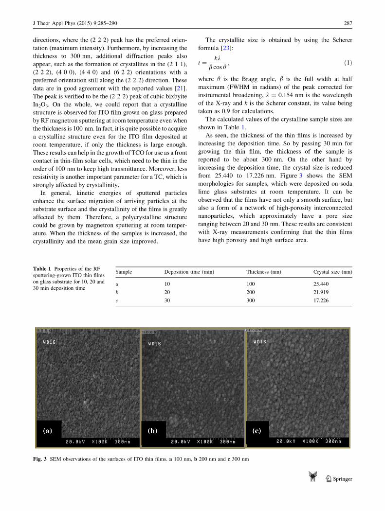
from 25.440 to 17.226 nm. Figure 3 shows the SEM
morphologies for samples, which were deposited on soda
lime glass substrates at room temperature. It can be
observed that the films have not only a smooth surface, but
also a form of a network of high-porosity interconnected
nanoparticles, which approximately have a pore size
ranging between 20 and 30 nm. These results are consistent
with X-ray measurements confirming that the thin films
have high porosity and high surface area.
Table 1 Properties of the RF
sputtering-grown ITO thin films
on glass substrate for 10, 20 and
30 min deposition time
Sample Deposition time (min) Thickness (nm) Crystal size (nm)
a 10 100 25.440
b 20 200 21.919
c 30 300 17.226
Fig. 3 SEM observations of the surfaces of ITO thin films. a 100 nm, b 200 nm and c 300 nm
J Theor Appl Phys (2015) 9:285–290 287
123
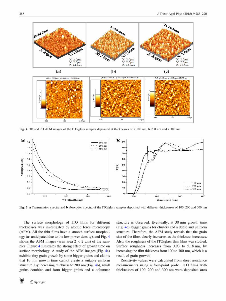
The surface morphology of ITO films for different
thicknesses was investigated by atomic force microscopy
(AFM). All the thin films have a smooth surface morphol-
ogy (as anticipated due to the low power density), and Fig. 4
shows the AFM images (scan area 2 9 2 lm) of the sam-
ples. Figure 4 illustrates the strong effect of growth time on
surface morphology. A study of the AFM images (Fig. 4a)
exhibits tiny grain growth by some bigger grains and claims
that 10 min growth time cannot create a suitable uniform
structure. By increasing thickness to 200 nm (Fig. 4b), small
grains combine and form bigger grains and a columnar
structure is observed. Eventually, at 30 min growth time
(Fig. 4c), bigger grains for clusters and a dense and uniform
structure. Therefore, the AFM study reveals that the grain
size of the films clearly increases as the thickness increases.
Also, the roughness of the ITO/glass thin films was studied.
Surface roughness increases from 3.93 to 5.18 nm, by
increasing the film thickness from 100 to 300 nm, which is a
result of grain growth.
Resistivity values were calculated from sheet resistance
measurements using a four-point probe. ITO films with
thicknesses of 100, 200 and 300 nm were deposited onto
Fig. 4 3D and 2D AFM images of the ITO/glass samples deposited at thicknesses of a 100 nm, b 200 nm and c 300 nm
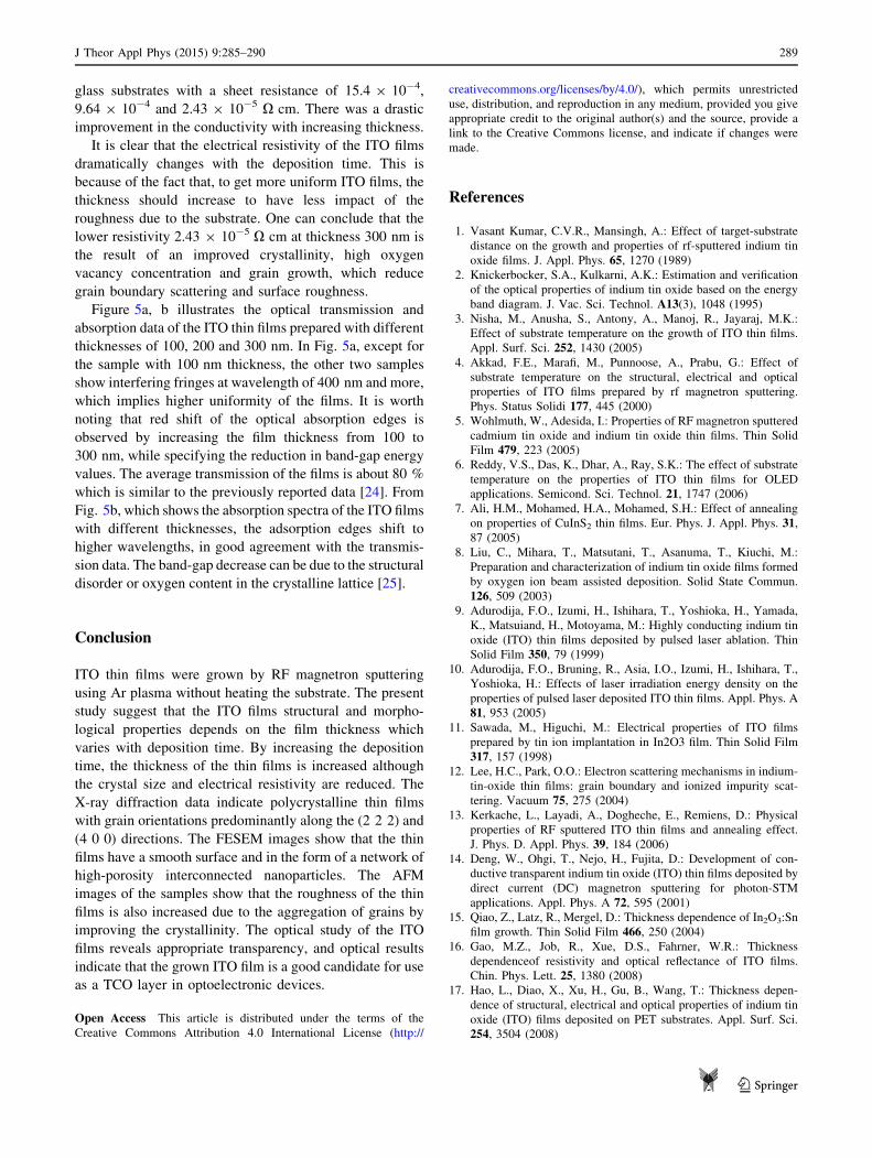
Fig. 5 a Transmission spectra and b absorption spectra of the ITO/glass samples deposited with different thicknesses of 100, 200 and 300 nm
288 J Theor Appl Phys (2015) 9:285–290
123
glass substrates with a sheet resistance of 15.4 9 10-4,
9.64 9 10-4 and 2.43 9 10-5 X cm. There was a drastic
improvement in the conductivity with increasing thickness.
It is clear that the electrical resistivity of the ITO films
dramatically changes with the deposition time. This is
because of the fact that, to get more uniform ITO films, the
thickness should increase to have less impact of the
roughness due to the substrate. One can conclude that the
lower resistivity 2.43 9 10-5 X cm at thickness 300 nm is
the result of an improved crystallinity, high oxygen
vacancy concentration and grain growth, which reduce
grain boundary scattering and surface roughness.
Figure 5a, b illustrates the optical transmission and
absorption data of the ITO thin films prepared with different
thicknesses of 100, 200 and 300 nm. In Fig. 5a, except for
the sample with 100 nm thickness, the other two samples
show interfering fringes at wavelength of 400 nm and more,
which implies higher uniformity of the films. It is worth
noting that red shift of the optical absorption edges is
observed by increasing the film thickness from 100 to
300 nm, while specifying the reduction in band-gap energy
values. The average transmission of the films is about 80 %
which is similar to the previously reported data [24]. From
Fig. 5b, which shows the absorption spectra of the ITO films
with different thicknesses, the adsorption edges shift to
higher wavelengths, in good agreement with the transmis-
sion data. The band-gap decrease can be due to the structural
disorder or oxygen content in the crystalline lattice [25].
Conclusion
ITO thin films were grown by RF magnetron sputtering
using Ar plasma without heating the substrate. The present
study suggest that the ITO films structural and morpho-
logical properties depends on the film thickness which
varies with deposition time. By increasing the deposition
time, the thickness of the thin films is increased although
the crystal size and electrical resistivity are reduced. The
X-ray diffraction data indicate polycrystalline thin films
with grain orientations predominantly along the (2 2 2) and
(4 0 0) directions. The FESEM images show that the thin
films have a smooth surface and in the form of a network of
high-porosity interconnected nanoparticles. The AFM
images of the samples show that the roughness of the thin
films is also increased due to the aggregation of grains by
improving the crystallinity. The optical study of the ITO
films reveals appropriate transparency, and optical results
indicate that the grown ITO film is a good candidate for use
as a TCO layer in optoelectronic devices.
Open Access This article is distributed under the terms of the
Creative Commons Attribution 4.0 International License (http://
creativecommons.org/licenses/by/4.0/), which permits unrestricted
use, distribution, and reproduction in any medium, provided you give
appropriate credit to the original author(s) and the source, provide a
link to the Creative Commons license, and indicate if changes were
made.
References
1. Vasant Kumar, C.V.R., Mansingh, A.: Effect of target-substrate
distance on the growth and properties of rf-sputtered indium tin
oxide films. J. Appl. Phys. 65, 1270 (1989)
2. Knickerbocker, S.A., Kulkarni, A.K.: Estimation and verification
of the optical properties of indium tin oxide based on the energy
band diagram. J. Vac. Sci. Technol. A13(3), 1048 (1995)
3. Nisha, M., Anusha, S., Antony, A., Manoj, R., Jayaraj, M.K.:
Effect of substrate temperature on the growth of ITO thin films.
Appl. Surf. Sci. 252, 1430 (2005)
4. Akkad, F.E., Marafi, M., Punnoose, A., Prabu, G.: Effect of
substrate temperature on the structural, electrical and optical
properties of ITO films prepared by rf magnetron sputtering.
Phys. Status Solidi 177, 445 (2000)
5. Wohlmuth, W., Adesida, I.: Properties of RF magnetron sputtered
cadmium tin oxide and indium tin oxide thin films. Thin Solid
Film 479, 223 (2005)
6. Reddy, V.S., Das, K., Dhar, A., Ray, S.K.: The effect of substrate
temperature on the properties of ITO thin films for OLED
applications. Semicond. Sci. Technol. 21, 1747 (2006)
7. Ali, H.M., Mohamed, H.A., Mohamed, S.H.: Effect of annealing
on properties of CuInS2 thin films. Eur. Phys. J. Appl. Phys. 31,87 (2005)
8. Liu, C., Mihara, T., Matsutani, T., Asanuma, T., Kiuchi, M.:
Preparation and characterization of indium tin oxide films formed
by oxygen ion beam assisted deposition. Solid State Commun.
126, 509 (2003)
9. Adurodija, F.O., Izumi, H., Ishihara, T., Yoshioka, H., Yamada,
K., Matsuiand, H., Motoyama, M.: Highly conducting indium tin
oxide (ITO) thin films deposited by pulsed laser ablation. Thin
Solid Film 350, 79 (1999)
10. Adurodija, F.O., Bruning, R., Asia, I.O., Izumi, H., Ishihara, T.,
Yoshioka, H.: Effects of laser irradiation energy density on the
properties of pulsed laser deposited ITO thin films. Appl. Phys. A
81, 953 (2005)
11. Sawada, M., Higuchi, M.: Electrical properties of ITO films
prepared by tin ion implantation in In2O3 film. Thin Solid Film
317, 157 (1998)
12. Lee, H.C., Park, O.O.: Electron scattering mechanisms in indium-
tin-oxide thin films: grain boundary and ionized impurity scat-
tering. Vacuum 75, 275 (2004)
13. Kerkache, L., Layadi, A., Dogheche, E., Remiens, D.: Physical
properties of RF sputtered ITO thin films and annealing effect.
J. Phys. D. Appl. Phys. 39, 184 (2006)
14. Deng, W., Ohgi, T., Nejo, H., Fujita, D.: Development of con-
ductive transparent indium tin oxide (ITO) thin films deposited by
direct current (DC) magnetron sputtering for photon-STM
applications. Appl. Phys. A 72, 595 (2001)
15. Qiao, Z., Latz, R., Mergel, D.: Thickness dependence of In2O3:Sn
film growth. Thin Solid Film 466, 250 (2004)
16. Gao, M.Z., Job, R., Xue, D.S., Fahrner, W.R.: Thickness
dependenceof resistivity and optical reflectance of ITO films.
Chin. Phys. Lett. 25, 1380 (2008)
17. Hao, L., Diao, X., Xu, H., Gu, B., Wang, T.: Thickness depen-
dence of structural, electrical and optical properties of indium tin
oxide (ITO) films deposited on PET substrates. Appl. Surf. Sci.
254, 3504 (2008)
J Theor Appl Phys (2015) 9:285–290 289
123
18. Guillen, C., Herrero, J.: Influence of the film thickness on the
structure, optical and electrical properties of ITO coatings
deposited by sputtering at room temperature on glass and plastic
substrates. Semicond. Sci. Technol. 23, 075002 (2008)
19. Kim, D.H., Park, M.R., Lee, H.J., Lee, G.H.: Thickness depen-
dence of electrical properties of ITO film deposited on a plastic
substrate by RF magnetron sputtering. Appl. Surf. Sci. 253, 409(2006)
20. Kim, H., Horwitz, J.S., Kushto, G., Pique, A., Kafafi, Z.H., Gil-
more, C.M., Chrisey, D.B.: Effect of film thickness on the
properties of indium tin oxide thin films. J. Appl. Phys. 88, 6021(2000)
21. Liu, C., Matsutani, T., Asanuma, T., Murai, K., Kiuchi, M.,
Alves, E., Reis, M.: Room-temperature growth of crystalline
indium tin oxide films on glass using low energy oxygen ion
beam assisted deposition. J. Appl. Phys. 93, 2262 (2003)
22. Kumar, K.J., Raju, N.R.C., Subrahmanyam, A.: Thickness
dependent physical and photocatalytic properties of ITO thin
films prepared by reactive DC magnetron sputtering. Appl. Surf.
Sci. 257(7), 3075–3080 (2011)
23. Nair, P.K., Gomez-Daza, O., Readigos, A.A.C., Campos, J., Nair,
M.T.S.: Formation of conductive CdO layer on CdS thin films
during air heating. Semicond. Sci. Technol. 16(8), 651–656
(2001)
24. Heo, K.C., Sohn, Y., Gwag, J.S.: Effects of an additional mag-
netic field in ITO thin film deposition by magnetron sputtering.
Ceram int 41, 617–621 (2015)
25. Bouzidi, A., Omri, K., El Mir Mabrouk, L., Guermazi, H.:
Preparation, structural and optical investigations of ITO
nanopowder and ITO/epoxy nanocomposites. Mater. Sci. Semi-
cond. Process. 39, 536–543 (2015)
290 J Theor Appl Phys (2015) 9:285–290
123