Embed Size (px)
Citation preview
Solid State Communications 149 (2009) 1650–1653
Contents lists available at ScienceDirect
Solid State Communications
journal homepage: www.elsevier.com/locate/ssc
Structural and magnetic properties of electrodeposited Cobalt nanowire arraysS. Sharma a, A. Barman a,∗, M. Sharma b, L.R. Shelford c, V.V. Kruglyak c, R.J. Hicken ca Department of Physics, Indian Institute of Technology Delhi, Hauz Khas, New Delhi-110016, Indiab Centre for Applied Research in Electronics, Indian Institute of Technology Delhi, Hauz Khas, New Delhi-110016, Indiac School of Physics, University of Exeter, Stocker Road, Exeter EX4 4QL, United Kingdom
a r t i c l e i n f o
Article history:Received 3 June 2009Accepted 20 June 2009 by A.H. MacDonaldAvailable online 26 June 2009
PACS:79.60.Jv74.25.Ha75.60.Ej
Keywords:A. Magnetic nanowiresB. ElectrodepositionD. Magnetisation reversalE. Magneto-optical Kerr effect
a b s t r a c t
Ordered magnetic nanowires have tremendous potential in future magnetic storage and high frequencymagnetic logic devices. Here, we present the fabrication of ordered arrays of Cobalt nanowiresby electrodeposition through porous polycarbonate membranes. Vertically and horizontally alignednanowires were produced in presence of an external bias field during post deposition etching of thepolycarbonate membrane. Structural and compositional analyses have been carried out to establishthe material and structural purity. The magneto-optical Kerr effect was employed to measure themagnetic hysteresis loops for the nanowires assembled in the substrate plane. A good magneto-opticalsignal to noise ratio is observed with clean ferromagnetic hysteresis loops. The loops measured withexternal magnetic field applied parallel and perpendicular to the axis of the nanowires show a cleardifference in the shape and the coercive field, indicating the effect of shape anisotropy in these samples.Micromagnetic simulations were performed to understand the experimental results and to obtain insightto the magnetization reversal mechanism in magnetic nanowires.
© 2009 Elsevier Ltd. All rights reserved.
1. Introduction
Magnetic nanostructures will form the building blocks forfuture magnetic data storage such as patterned and perpendicularmagnetic media [1]. Beyond that they have tremendous potentialfor applications in magnetic magnetic field sensors [2] andmagnetic logic devices [3] in which magnetic domain movementor spin waves may be used as an information carrier. Twovery important aspects of nanomagnets are the fabrication ofordered arrays in a cost effective manner and to probe theirstatic and dynamic magnetic properties by highly sensitive nondestructive techniques. A lot of effort has been directed towardsfabricating nanomagnet arrays by slow and expensive but precisetechniques such as optical and electron beam lithography [4].Recent developments of chemical [5,6] and electrochemical [7,8]methods combined with self assembly processes have fueledinterest into the fabrication of ordered magnetic nanostructures.On the other hand reports on characterization of their structuraland magnetic properties have also been started [5–8]. However, alot more progress is required in the fabrication of ordered arraysof high aspect ratio nanomagnets in wire and rod shapes with
∗ Corresponding address: Department of Materials Science, S. N. Bose NationalCentre For Basic Sciences, Block JD, Sector III, Salt lake, Kolkata 700 098, India Tel.:+91 33 23355706; fax: +91 33 23353477.E-mail address: [email protected] (A. Barman).
0038-1098/$ – see front matter© 2009 Elsevier Ltd. All rights reserved.doi:10.1016/j.ssc.2009.06.025
desired magnetic properties before they could be introduced intoapplications.Themagneto-optical Kerr effect (MOKE) [9,10] is a very popular
technique for probing the static [11] and time-resolved [12–14]magnetization processes of nanomagnets and also due to its usein magneto-optical data storage. Static and time-resolved MOKEshave made use of array measurements due to the enhancement ofthe total MOKE signal from a large number of elements in an arrayfalling within the area of a diffraction limited laser spot (∼1 µm).This gives rise to a collective response due to the ensemble effect,which is reflected in the magnetic switching field distribution(SFD) [15], and collective precessional modes in magnetizationdynamics [16]. If precessional switching has to be introducedin the read–write processes of magnetic data storage, the aboveissues must be understood and controlled. Very few studies ofmagnetization dynamics in nanomagnet arrays have been reportedso far [12–14,16]. An interesting prospect lies in the measurementof static and dynamic magnetization processes of electrodepositeddipolar coupled magnetic nanowire arrays by magneto-opticalKerr effect. However, this requires an enhancement of themagneto-optical signal to noise ratio from electrodepositednanomagnet arrays. Here, we report the fabrication of orderedCobalt nanowires by templated electrodeposition and assemblingof the freestanding nanowires vertically or horizontally on theplane of the substrate. We also report the measurement ofmagnetic hysteresis loops from those nanowires by MOKE. Finally,we discuss themagnetization reversal process in Cobalt nanowireswith the aid of micromagnetic simulations.
S. Sharma et al. / Solid State Communications 149 (2009) 1650–1653 1651
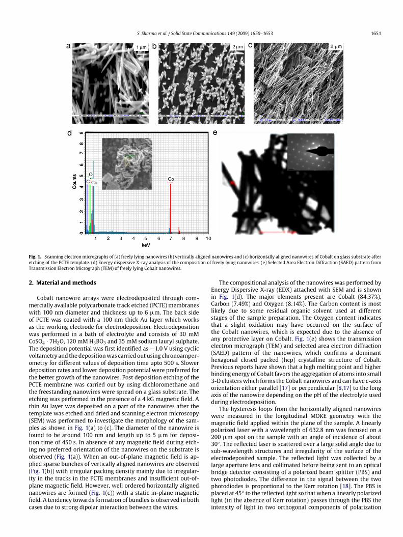
Fig. 1. Scanning electron micrographs of (a) freely lying nanowires (b) vertically aligned nanowires and (c) horizontally aligned nanowires of Cobalt on glass substrate afteretching of the PCTE template. (d) Energy dispersive X-ray analysis of the composition of freely lying nanowires. (e) Selected Area Electron Diffraction (SAED) pattern fromTransmission Electron Micrograph (TEM) of freely lying Cobalt nanowires.
2. Material and methods
Cobalt nanowire arrays were electrodeposited through com-mercially available polycarbonate track etched (PCTE) membraneswith 100 nm diameter and thickness up to 6 µm. The back sideof PCTE was coated with a 100 nm thick Au layer which worksas the working electrode for electrodeposition. Electrodepositionwas performed in a bath of electrolyte and consists of 30 mMCoSO4 · 7H2O, 120 mM H3BO3 and 35 mM sodium lauryl sulphate.The deposition potential was first identified as−1.0 V using cyclicvoltametry and the depositionwas carried out using chronoamper-ometry for different values of deposition time upto 500 s. Slowerdeposition rates and lower deposition potential were preferred forthe better growth of the nanowires. Post deposition etching of thePCTE membrane was carried out by using dichloromethane andthe freestanding nanowires were spread on a glass substrate. Theetching was performed in the presence of a 4 kG magnetic field. Athin Au layer was deposited on a part of the nanowires after thetemplate was etched and dried and scanning electron microscopy(SEM) was performed to investigate the morphology of the sam-ples as shown in Fig. 1(a) to (c). The diameter of the nanowire isfound to be around 100 nm and length up to 5 µm for deposi-tion time of 450 s. In absence of any magnetic field during etch-ing no preferred orientation of the nanowires on the substrate isobserved (Fig. 1(a)). When an out-of-plane magnetic field is ap-plied sparse bunches of vertically aligned nanowires are observed(Fig. 1(b)) with irregular packing density mainly due to irregular-ity in the tracks in the PCTE membranes and insufficient out-of-plane magnetic field. However, well ordered horizontally alignednanowires are formed (Fig. 1(c)) with a static in-plane magneticfield. A tendency towards formation of bundles is observed in bothcases due to strong dipolar interaction between the wires.
The compositional analysis of the nanowires was performed byEnergy Dispersive X-ray (EDX) attached with SEM and is shownin Fig. 1(d). The major elements present are Cobalt (84.37%),Carbon (7.49%) and Oxygen (8.14%). The Carbon content is mostlikely due to some residual organic solvent used at differentstages of the sample preparation. The Oxygen content indicatesthat a slight oxidation may have occurred on the surface ofthe Cobalt nanowires, which is expected due to the absence ofany protective layer on Cobalt. Fig. 1(e) shows the transmissionelectron micrograph (TEM) and selected area electron diffraction(SAED) pattern of the nanowires, which confirms a dominanthexagonal closed packed (hcp) crystalline structure of Cobalt.Previous reports have shown that a high melting point and higherbinding energy of Cobalt favors the aggregation of atoms into small3-D clusterswhich forms the Cobalt nanowires and can have c-axisorientation either parallel [17] or perpendicular [8,17] to the longaxis of the nanowire depending on the pH of the electrolyte usedduring electrodeposition.The hysteresis loops from the horizontally aligned nanowires
were measured in the longitudinal MOKE geometry with themagnetic field applied within the plane of the sample. A linearlypolarized laser with a wavelength of 632.8 nm was focused on a200 µm spot on the sample with an angle of incidence of about30◦. The reflected laser is scattered over a large solid angle due tosub-wavelength structures and irregularity of the surface of theelectrodeposited sample. The reflected light was collected by alarge aperture lens and collimated before being sent to an opticalbridge detector consisting of a polarized beam splitter (PBS) andtwo photodiodes. The difference in the signal between the twophotodiodes is proportional to the Kerr rotation [18]. The PBS isplaced at 45◦ to the reflected light so thatwhen a linearly polarizedlight (in the absence of Kerr rotation) passes through the PBS theintensity of light in two orthogonal components of polarization
1652 S. Sharma et al. / Solid State Communications 149 (2009) 1650–1653
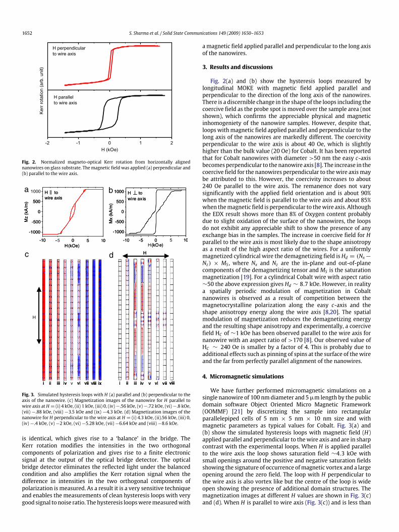
Fig. 2. Normalized magneto-optical Kerr rotation from horizontally alignednanowires on glass substrate. Themagnetic field was applied (a) perpendicular and(b) parallel to the wire axis.
a b
c d
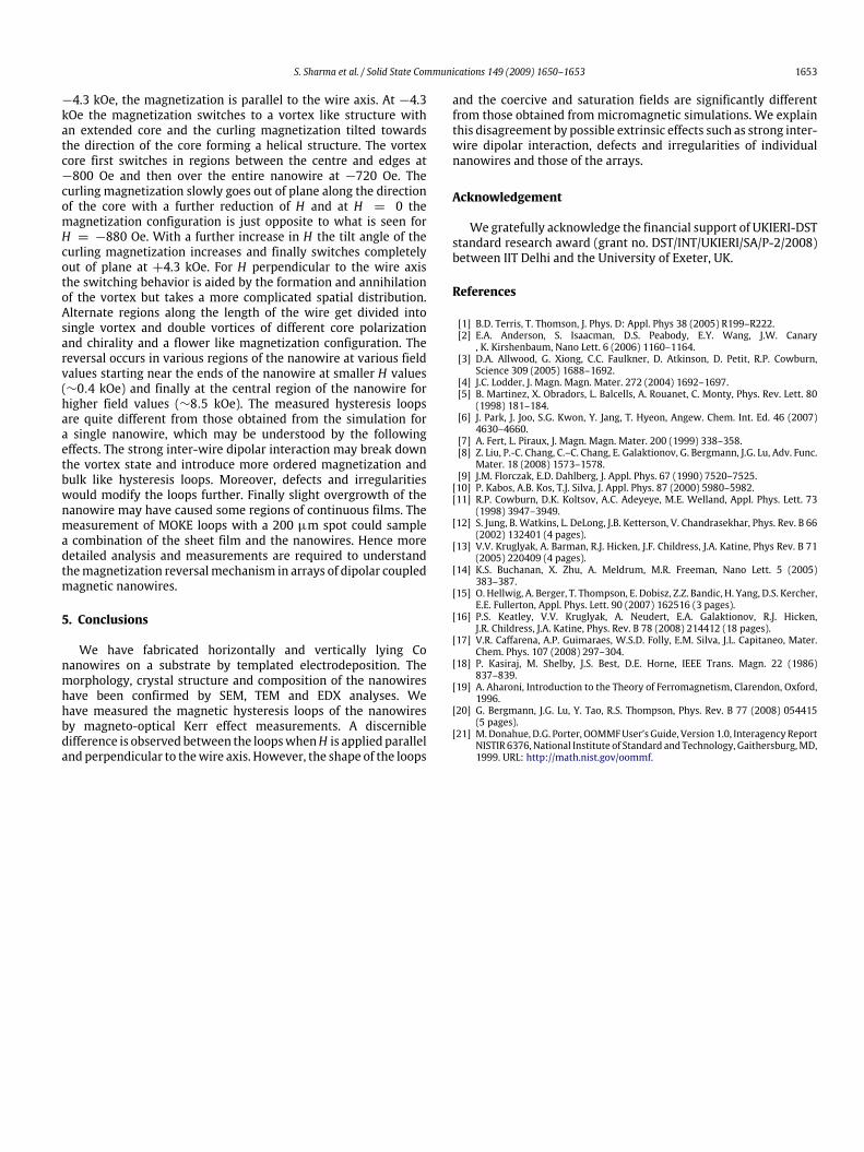
Fig. 3. Simulated hysteresis loops with H (a) parallel and (b) perpendicular to theaxis of the nanowire. (c) Magnetization images of the nanowire for H parallel towire axis atH = (i) 4 kOe, (ii) 1 kOe, (iii) 0, (iv)−.56 kOe, (v)−.72 kOe, (vi)−.8 kOe,(vii) −.88 kOe, (viii) −3.5 kOe and (ix) −4.3 kOe. (d) Magnetization images of thenanowire for H perpendicular to the wire axis at H = (i) 4.3 kOe, (ii).56 kOe, (iii) 0,(iv)−.4 kOe, (v)−2 kOe, (vi)−5.28 kOe, (vii)−6.64 kOe and (viii)−8.6 kOe.
is identical, which gives rise to a ‘balance’ in the bridge. TheKerr rotation modifies the intensities in the two orthogonalcomponents of polarization and gives rise to a finite electronicsignal at the output of the optical bridge detector. The opticalbridge detector eliminates the reflected light under the balancedcondition and also amplifies the Kerr rotation signal when thedifference in intensities in the two orthogonal components ofpolarization is measured. As a result it is a very sensitive techniqueand enables the measurements of clean hysteresis loops with verygood signal to noise ratio. The hysteresis loopsweremeasuredwith
amagnetic field applied parallel and perpendicular to the long axisof the nanowires.
3. Results and discussions
Fig. 2(a) and (b) show the hysteresis loops measured bylongitudinal MOKE with magnetic field applied parallel andperpendicular to the direction of the long axis of the nanowires.There is a discernible change in the shape of the loops including thecoercive field as the probe spot is moved over the sample area (notshown), which confirms the appreciable physical and magneticinhomogeniety of the nanowire samples. However, despite that,loopswithmagnetic field applied parallel and perpendicular to thelong axis of the nanowires are markedly different. The coercivityperpendicular to the wire axis is about 40 Oe, which is slightlyhigher than the bulk value (20 Oe) for Cobalt. It has been reportedthat for Cobalt nanowires with diameter >50 nm the easy c-axisbecomesperpendicular to thenanowire axis [8]. The increase in thecoercive field for the nanowires perpendicular to thewire axismaybe attributed to this. However, the coercivity increases to about240 Oe parallel to the wire axis. The remanence does not varysignificantly with the applied field orientation and is about 90%when the magnetic field is parallel to the wire axis and about 85%when themagnetic field is perpendicular to thewire axis. Althoughthe EDX result shows more than 8% of Oxygen content probablydue to slight oxidation of the surface of the nanowires, the loopsdo not exhibit any appreciable shift to show the presence of anyexchange bias in the samples. The increase in coercive field for Hparallel to the wire axis is most likely due to the shape anisotropyas a result of the high aspect ratio of the wires. For a uniformlymagnetized cylindrical wire the demagnetizing field isHd = (Nx−Nz) × MS , where Nx and Nz are the in-plane and out-of-planecomponents of the demagnetizing tensor andMS is the saturationmagnetization [19]. For a cylindrical Cobalt wire with aspect ratio∼50 the above expression gives Hd ∼ 8.7 kOe. However, in realitya spatially periodic modulation of magnetization in Cobaltnanowires is observed as a result of competition between themagnetocrystalline polarization along the easy c-axis and theshape anisotropy energy along the wire axis [8,20]. The spatialmodulation of magnetization reduces the demagnetizing energyand the resulting shape anisotropy and experimentally, a coercivefield HC of ∼1 kOe has been observed parallel to the wire axis fornanowire with an aspect ratio of >170 [8]. Our observed value ofHC ∼ 240 Oe is smaller by a factor of 4. This is probably due toadditional effects such as pinning of spins at the surface of thewireand the far from perfectly parallel alignment of the nanowires.
4. Micromagnetic simulations
We have further performed micromagnetic simulations on asingle nanowire of 100 nmdiameter and 5µm length by the publicdomain software Object Oriented Micro Magnetic Framework(OOMMF) [21] by discretizing the sample into rectangularparallelepiped cells of 5 nm × 5 nm × 10 nm size and withmagnetic parameters as typical values for Cobalt. Fig. 3(a) and(b) show the simulated hysteresis loops with magnetic field (H)applied parallel and perpendicular to thewire axis and are in sharpcontrast with the experimental loops. When H is applied parallelto the wire axis the loop shows saturation field ∼4.3 kOe withsmall openings around the positive and negative saturation fieldsshowing the signature of occurrence ofmagnetic vortex and a largeopening around the zero field. The loop with H perpendicular tothe wire axis is also vortex like but the centre of the loop is wideopen showing the presence of additional domain structures. Themagnetization images at different H values are shown in Fig. 3(c)and (d). When H is parallel to wire axis (Fig. 3(c)) and is less than
S. Sharma et al. / Solid State Communications 149 (2009) 1650–1653 1653
−4.3 kOe, the magnetization is parallel to the wire axis. At −4.3kOe the magnetization switches to a vortex like structure withan extended core and the curling magnetization tilted towardsthe direction of the core forming a helical structure. The vortexcore first switches in regions between the centre and edges at−800 Oe and then over the entire nanowire at −720 Oe. Thecurling magnetization slowly goes out of plane along the directionof the core with a further reduction of H and at H = 0 themagnetization configuration is just opposite to what is seen forH = −880 Oe. With a further increase in H the tilt angle of thecurling magnetization increases and finally switches completelyout of plane at +4.3 kOe. For H perpendicular to the wire axisthe switching behavior is aided by the formation and annihilationof the vortex but takes a more complicated spatial distribution.Alternate regions along the length of the wire get divided intosingle vortex and double vortices of different core polarizationand chirality and a flower like magnetization configuration. Thereversal occurs in various regions of the nanowire at various fieldvalues starting near the ends of the nanowire at smaller H values(∼0.4 kOe) and finally at the central region of the nanowire forhigher field values (∼8.5 kOe). The measured hysteresis loopsare quite different from those obtained from the simulation fora single nanowire, which may be understood by the followingeffects. The strong inter-wire dipolar interaction may break downthe vortex state and introduce more ordered magnetization andbulk like hysteresis loops. Moreover, defects and irregularitieswould modify the loops further. Finally slight overgrowth of thenanowire may have caused some regions of continuous films. Themeasurement of MOKE loops with a 200 µm spot could samplea combination of the sheet film and the nanowires. Hence moredetailed analysis and measurements are required to understandthemagnetization reversalmechanism in arrays of dipolar coupledmagnetic nanowires.
5. Conclusions
We have fabricated horizontally and vertically lying Conanowires on a substrate by templated electrodeposition. Themorphology, crystal structure and composition of the nanowireshave been confirmed by SEM, TEM and EDX analyses. Wehave measured the magnetic hysteresis loops of the nanowiresby magneto-optical Kerr effect measurements. A discernibledifference is observed between the loopswhenH is applied paralleland perpendicular to thewire axis. However, the shape of the loops
and the coercive and saturation fields are significantly differentfrom those obtained frommicromagnetic simulations. We explainthis disagreement by possible extrinsic effects such as strong inter-wire dipolar interaction, defects and irregularities of individualnanowires and those of the arrays.
Acknowledgement
We gratefully acknowledge the financial support of UKIERI-DSTstandard research award (grant no. DST/INT/UKIERI/SA/P-2/2008)between IIT Delhi and the University of Exeter, UK.
References
[1] B.D. Terris, T. Thomson, J. Phys. D: Appl. Phys 38 (2005) R199–R222.[2] E.A. Anderson, S. Isaacman, D.S. Peabody, E.Y. Wang, J.W. Canary, K. Kirshenbaum, Nano Lett. 6 (2006) 1160–1164.
[3] D.A. Allwood, G. Xiong, C.C. Faulkner, D. Atkinson, D. Petit, R.P. Cowburn,Science 309 (2005) 1688–1692.
[4] J.C. Lodder, J. Magn. Magn. Mater. 272 (2004) 1692–1697.[5] B. Martinez, X. Obradors, L. Balcells, A. Rouanet, C. Monty, Phys. Rev. Lett. 80(1998) 181–184.
[6] J. Park, J. Joo, S.G. Kwon, Y. Jang, T. Hyeon, Angew. Chem. Int. Ed. 46 (2007)4630–4660.
[7] A. Fert, L. Piraux, J. Magn. Magn. Mater. 200 (1999) 338–358.[8] Z. Liu, P.-C. Chang, C.–C. Chang, E. Galaktionov, G. Bergmann, J.G. Lu, Adv. Func.Mater. 18 (2008) 1573–1578.
[9] J.M. Florczak, E.D. Dahlberg, J. Appl. Phys. 67 (1990) 7520–7525.[10] P. Kabos, A.B. Kos, T.J. Silva, J. Appl. Phys. 87 (2000) 5980–5982.[11] R.P. Cowburn, D.K. Koltsov, A.C. Adeyeye, M.E. Welland, Appl. Phys. Lett. 73
(1998) 3947–3949.[12] S. Jung, B. Watkins, L. DeLong, J.B. Ketterson, V. Chandrasekhar, Phys. Rev. B 66
(2002) 132401 (4 pages).[13] V.V. Kruglyak, A. Barman, R.J. Hicken, J.F. Childress, J.A. Katine, Phys Rev. B 71
(2005) 220409 (4 pages).[14] K.S. Buchanan, X. Zhu, A. Meldrum, M.R. Freeman, Nano Lett. 5 (2005)
383–387.[15] O. Hellwig, A. Berger, T. Thompson, E. Dobisz, Z.Z. Bandic, H. Yang, D.S. Kercher,
E.E. Fullerton, Appl. Phys. Lett. 90 (2007) 162516 (3 pages).[16] P.S. Keatley, V.V. Kruglyak, A. Neudert, E.A. Galaktionov, R.J. Hicken,
J.R. Childress, J.A. Katine, Phys. Rev. B 78 (2008) 214412 (18 pages).[17] V.R. Caffarena, A.P. Guimaraes, W.S.D. Folly, E.M. Silva, J.L. Capitaneo, Mater.
Chem. Phys. 107 (2008) 297–304.[18] P. Kasiraj, M. Shelby, J.S. Best, D.E. Horne, IEEE Trans. Magn. 22 (1986)
837–839.[19] A. Aharoni, Introduction to the Theory of Ferromagnetism, Clarendon, Oxford,
1996.[20] G. Bergmann, J.G. Lu, Y. Tao, R.S. Thompson, Phys. Rev. B 77 (2008) 054415
(5 pages).[21] M.Donahue, D.G. Porter, OOMMFUser’s Guide, Version 1.0, InteragencyReport
NISTIR 6376, National Institute of Standard and Technology, Gaithersburg,MD,1999. URL: http://math.nist.gov/oommf.