Embed Size (px)
Citation preview

Strontium Stannate – An Emerging Wide Gap Semiconductor for
Field-Effect Transistor Applications
A THESIS
SUBMITTED TO THE FACULTY OF THE
UNIVERSITY OF MINNESOTA
BY
VENKATA RAGHAVA SARAN KUMAR CHAGANTI
IN PARTIAL FULFILLMENT OF THE REQUIREMENTS
FOR THE DEGREE OF
Doctor of Philosophy
Advisor: Professor Steven John Koester
June 2020

© VR Saran Kumar Chaganti 2020
ALL RIGHTS RESERVED

i
Acknowledgements
I would like to express a special thanks of gratitude to my advisor Prof. Steven J. Koester
whose continuous encouragement and guidance enabled the conception and completion of
this undertaking. He remains a constant source of inspiration. His support during the
entirety of my graduate studies, his patience, immense knowledge, and sharp research
acumen not only helped me in this journey but made it a pleasant and enjoyable one. I
could not have asked for a better mentor than him. I am grateful to him for believing in me
and for providing me with opportunities and the best possible atmosphere to work in.
Besides my advisor, I would like to thank the rest of my thesis committee members,
namely, Prof. Stephen Campbell, Prof. Sang-Hyun Oh, and Prof. Bharat Jalan, for their
patience, time, and valuable insights. I would also like to extend my gratitude to Prof. Sarah
Swisher for her time and advice while serving on my oral preliminary examination
committee.
I would like to thank my parents for inculcating qualities of discipline and hard work in
me. Their constant encouragement and support made possible everything that I have
accomplished in my life, including this work. This work could not have been possible
without their sacrifice and perseverance. I would further like to thank my sisters Hima
Bindu Gollapudi and Hari Priya Yellemraju who have played an auxiliary but vital role in
shaping my life. Their love and affection helped me overcome all the hardships that I had

ii
faced. I would also like to thank my sister’ families for their support and my wonderful and
enthusiastic nephews, who perhaps helped me learn the most valuable lessons in my life.
A special mention for Prof. Bharat Jalan, for providing this collaborative opportunity with
him and his team and valuable guidance. Without the hard work and efforts of Prof. Jalan’s
research lab members, in particular, Dr. Abhinav Prakash, Tristan K. Truttmann, Dr. Tianqi
Wang, Fengdeng Liu, Dr. Laxman R. Thoutam, and William Nunn, I cannot imagine
completing even a small part of this dissertation work. Discussions with Prof. Bharat Jalan,
Abhinav Prakash, and Tristan K. Truttmann, yielded many useful ideas and solutions that
helped me during the course this work.
I would like to thank my colleagues Rui Ma, Qun Su, Dr. Yao Zhang, Jiaxuan Wen, and
Prafful Golani who I have had the pleasure of working and collaborating with. It was an
absolute pleasure to discuss and work with them on various projects. I would like to thank
Dr. Yulong Li who had patiently taught me various fabrication techniques and processes
during the initial phase. Additionally, I would like to thank all the remaining group
members, namely, Dr. Jiaxi Hu, Dr. Matt Robbins, Dr. Chaitanya Kshirsagar, Dr. Nazila
Haratipour, Dr. Yoska Anugrah, Dr. Andrew Stephan, Dr. Yang Su, Dr. Mahmoud Atalla,
Dr. Seon Namgung, Dr. Sandhaya Koirala, Dr. Dongjea Seo, Prafful Golani, Jiaxuan Wen,
Nyssa Capman, Lun Jin, Prakash Palamedu Sundaram, Ruixue Li, and Chin Hsiang Liao,
for all the valuable discussions and for creating a friendly, sharing, and competitive but
enjoyable atmosphere.
I would also like to thank all the Minnesota Nano Center staff, namely, Tony Whipple,
Kevin Roberts, Mark Fisher, Lage von Dissen, Glenn Kuschke, Terry Brough, Paul
Kimani, late Gary Olin, Rich Macy, Robert Amundson, Bashir Jama, Laura Parmeter, Matt
Lowe, Becky von Dissen, Sherri Quick, Assefa Geleta, Jim Marti, and Greg Cibuzar. Their
hard work and dedication helped keep the cleanroom facilities operational and enabled the
work of numerous researchers and students. I significantly benefitted from the valuable
inputs provided by several of the above staff members and their knowledge, which greatly
simplified my work and helped resolve many process issues during the course of my
graduate life.

iii
I would like to thank the Department of Electrical and Computer Engineering (ECE) and
Linda Jagerson, ECE graduate student advisor, who have provided me with all the
resources needed for completion of my research and education. For enabling the
coursework that immensely helped me and all the other graduate students, I would like to
thank the Department of Chemical and Material Science, the School of Physics and
Astronomy, the Department of Chemistry, and the College of Science and Engineering.
I would also like to thank my former colleagues at Broadcom Corporation, India, and all
the Professors and members of the Birla Institute of Technology and Science, Pilani for
helping me in the early phase of my academic and professional life. I would like to thank
my former advisor Prof. Jeong-Hyun Cho and my former group members Dr. Chao Liu,
Chunhui Dai, Kriti Agarwal, Dr. Deaha Jung for supporting me during the initial phase of
my graduate life.
Finally, I would then like to thank my fiancée, Santoshi Saravanan, whose entry into my
life in 2016, was a turning point that I cannot forget. My sincerest gratitude for her
unconditional support, love, and affection that not only helped me in difficult times but has
also made me a better person. You were the missing piece without which my life would
have had no meaning.

iv
Dedication
I humbly offer this dissertation as a homage to Goddess Saraswati who bestowed me with
the abilities to produce this work. I dedicate this work to the hindu guru parampara whose
guidance has empowered me to make the appropriate decisions at every step of my life. I
also dedicate this work to every single life on this planet that has influenced me and
contributed to molding me into the person that I am.
To my parents, my sisters, my family, and my love, …
v
Abstract
Perovskite oxides are a promising family of materials with the potential for enabling the
development of advanced novel electronic device components. However, the lack of an
appropriate channel material has hindered the development of game-changing perovskite-
based electronic devices. Perovskite stannates are emerging tin-based perovskite oxide
semiconductors that have all the requisite material properties for a channel material and are
capable of high electron mobilities at unusually high carrier concentrations. Among the
perovskite stannates, barium stannate (BSO) has been the most popularly researched
material. Strontium stannate (SSO), another interesting perovskite stannate, has been
relatively less explored, even though by virtue of its smaller lattice constant, it is more
amenable for heterostructure growth than BSO and for eventual integration with other
perovskite oxide materials of novel technological interest. SSO also has a wide band gap
in the range of 4-5 eV, which makes it particularly well suited to high-power and radio
frequency (RF) applications. These properties provided us enough motivation to explore
SSO for field-effect transistor (FET) applications.
In this dissertation, the demonstration of first-ever SSO-based FETs with record
performance for any stannate-based FET is presented. Further, the challenge of producing
low resistance ohmic contacts to SSO is addressed through a systematic study, and
optimized contacts for use in FETs are demonstrated. Improvement in performance over
our previously reported SSO-based FETs is presented by utilizing a bi-layer film structure

vi
and RF operation in SSO-based FETs is also reported. This study lays the foundation for
the development of future high-performance and novel perovskite devices.

vii
Contents
Acknowledgements . . . . . . . . . . . . . . . . . . . . . . . . . . . . . . . . . . . . .i
Dedication . . . . . . . . . . . . . . . . . . . . . . . . . . . . . . . . . . . . . . . . .iv
Abstract . . . . . . . . . . . . . . . . . . . . . . . . . . . . . . . . . . . . . . . . . . .v
List of Tables . . . . . . . . . . . . . . . . . . . . . . . . . . . . . . . . . . . . . . . .x
List of Figures . . . . . . . . . . . . . . . . . . . . . . . . . . . . . . . . . . . . . . .xi
1. Introduction . . . . . . . . . . . . . . . . . . . . . . . . . . . . . . . . . . . . . .1
1.1 Perovskite Oxide Materials for Transistor Applications . . . . . . . . . . . . .4
1.1.1 Perovskite Oxides as Semiconductor Channel Materials . . . . . . . .7
1.2 Perovskite Stannates . . . . . . . . . . . . . . . . . . . . . . . . . . . . . . .9
1.2.1 Material Growth . . . . . . . . . . . . . . . . . . . . . . . . . . . .10
1.2.2 Barium Stannate . . . . . . . . . . . . . . . . . . . . . . . . . . . .12
1.2.2.1 Crystal and Band Structures . . . . . . . . . . . . . . . . .13

viii
1.2.2.2 Mobility . . . . . . . . . . . . . . . . . . . . . . . . . . .15
1.2.3 Strontium Stannate . . . . . . . . . . . . . . . . . . . . . . . . . . .18
1.2.3.1 Crystal and Band Structures . . . . . . . . . . . . . . . . .19
1.2.3.2 Mobility and Surface Effects . . . . . . . . . . . . . . . .21
1.3 Early Perovskite Oxide Device Results . . . . . . . . . . . . . . . . . . . . .22
1.4 Dissertation Goal . . . . . . . . . . . . . . . . . . . . . . . . . . . . . . . . 24
2. Single-Layer MESFET Results . . . . . . . . . . . . . . . . . . . . . . . . . . .26
2.1 MESFET . . . . . . . . . . . . . . . . . . . . . . . . . . . . . . . . . . . . .27
2.2 Sentaurus TCAD Simulation . . . . . . . . . . . . . . . . . . . . . . . . . .28
2.3 Device Fabrication . . . . . . . . . . . . . . . . . . . . . . . . . . . . . . . .30
2.3.1 Photolithography Process and Alignment Marks . . . . . . . . . . . .32
2.3.2 Mesa Isolation . . . . . . . . . . . . . . . . . . . . . . . . . . . . . 33
2.3.3 Schottky and Ohmic Contacts . . . . . . . . . . . . . . . . . . . . .34
2.4 Device Measurement Results . . . . . . . . . . . . . . . . . . . . . . . . . . 35
2.4.1 Transfer-Length Method Results . . . . . . . . . . . . . . . . . . . .35
2.4.2 MESFET Characterization . . . . . . . . . . . . . . . . . . . . . . . 36
2.4.3 Contact and Device Degradation . . . . . . . . . . . . . . . . . . . .41
3. Ohmic Contact Optimization . . . . . . . . . . . . . . . . . . . . . . . . . . . .43
3.1 Band-Edge Work Function Metals . . . . . . . . . . . . . . . . . . . . . . .44
3.2 Transfer-Length Method Structures Fabrication . . . . . . . . . . . . . . . .47
3.2.1 Contact Passivation and Annealing . . . . . . . . . . . . . . . . . . .49
3.3 Measurement Results . . . . . . . . . . . . . . . . . . . . . . . . . . . . . .52
3.3.1 Comparison of Sc-, Mn-, and Ti-contacts . . . . . . . . . . . . . . .52
3.3.2 Comparison of Ti-contacts on Single- and Bi-layer Films . . . . . . .55

ix
4. Bi-Layer MESFET Results . . . . . . . . . . . . . . . . . . . . . . . . . . . . . .59
4.1 Device Fabrication . . . . . . . . . . . . . . . . . . . . . . . . . . . . . . . .61
4.1.1 Recess Etch . . . . . . . . . . . . . . . . . . . . . . . . . . . . . . .61
4.1.2 Schottky Gate Deposition. . . . . . . . . . . . . . . . . . . . . . . .64
4.2 Measurement Results . . . . . . . . . . . . . . . . . . . . . . . . . . . . . .64
4.2.1 Comparison of Recess and Control Devices with Ni Schottky Gates . .65
4.2.2 Pt Schottky Devices . . . . . . . . . . . . . . . . . . . . . . . . . . .68
4.2.2.1 Transient Device Behavior . . . . . . . . . . . . . . . . .68
4.2.2.2 Anomalous Behavior after Thermal Annealing . . . . . . .69
4.3 RF Measurement Results . . . . . . . . . . . . . . . . . . . . . . . . . . . .72
5. Outlook and Conclusions . . . . . . . . . . . . . . . . . . . . . . . . . . . . . . .74
6.1 Conclusion . . . . . . . . . . . . . . . . . . . . . . . . . . . . . . . . . . . .75
6.2 Proposed Future Work . . . . . . . . . . . . . . . . . . . . . . . . . . . . . .76
6.2.1 Achieving High-Power Operation . . . . . . . . . . . . . . . . . . .76
6.2.1.1 Inverse Capped Structure . . . . . . . . . . . . . . . . . . 79
6.2.2 Path Forward to Heterostructures . . . . . . . . . . . . . . . . . . . .80
Bibliography . . . . . . . . . . . . . . . . . . . . . . . . . . . . . . . . . . . . . . . .81
Appendix A: Optical Photolithography Process Flow . . . . . . . . . . . . . . . . .92
Appendix B: E-Beam Lithography Process Flow . . . . . . . . . . . . . . . . . . . .95

x
List of Tables
1.1 A non-exhaustive list of perovskite oxides and their proposed applications in FETs
[3-15]. . . . . . . . . . . . . . . . . . . . . . . . . . . . . . . . . . . . . . . . 6
1.2 Comparison of early perovskite oxide-based FET results. . . . . . . . . . . . . 23
2.1 Summary of simulation parameters used in SSO MESFET simulations. . . . . 29
3.1 Summary of properties of the films used for contact studies. . . . . . . . . . . 48
3.2 Summary of transfer-length method data obtained for Sc-, Mn-, and Ti-contacts on
SSO_heavy film. . . . . . . . . . . . . . . . . . . . . . . . . . . . . . . . . . 54
3.3 Summary of transfer-length method data obtained for Ti-contacts on SSO_control
and SSO_bilayer films. . . . . . . . . . . . . . . . . . . . . . . . . . . . . . . 56
4.1 Comparison of (a) recess MESFET and (b) regular MESFET structures. . . . . .61

xi
List of Figures
1.1 One, or a combination of functional materials may be integrated with field-effect
transistors (FETs) to improve performance and/or effectuate a unique
characteristic. Each oval shape represents an interesting physical property that may
be combined as suggested by overlapping shapes. . . . . . . . . . . . . . . . . .3
1.2 A perovskite unit cell showing the cations, A and B, and O-atom. This can be
understood as the basic skeletal structure from which all perovskite materials’
crystal structures can be derived through modifications dictated by changes in
atomic sizes and bond-angles. The octahedron represents the BO6 bonds. . . . . 4
1.3 A calculated band structure for SrTiO3 showing the relatively lesser dispersion near
the conduction band minimum (Γ). Figure adapted from [26]. . . . . . . . . . . 8
1.4 A schematic of a hybrid molecular beam epitaxy (MBE) chamber and its various
components. Sn precursor is supplied via a gas bubbler system, O2 precursor via an
RF plasma, and other cation or dopant precursors can be supplied using an effusion
cell. Figure adapted from [36]. . . . . . . . . . . . . . . . . . . . . . . . . . . .11
1.5 (a) A simple unit cell of a BaSnO3 (BSO) crystal. SnO6 bonds are represented by
the octahedron. (b) An alternate representation of the BSO crystal which shows the
shared octahedral network and the perfect cubic lattice arrangement. . . . . . . .14

xii
1.6 Calculated band structure of BaSnO3 showing a dispersive conduction band
minimum that results in a low effective mass. Indirect band gap of ~3 eV is also
shown (Γ and R). Figure adapted from [44]. . . . . . . . . . . . . . . . . . . . .14
1.7 Log-log plot of the Hall measured at 300 K vs carrier concentration that compares
the Hall of BaSnO3 with that of other transparent conducting oxides and
conventional semiconductors. Figure adapted from [31]. . . . . . . . . . . . . .15
1.8 Semi-log plot of the measured mobility in BaSnO3 vs n3D cm-3, plotted as a function
of different dislocation densities. Figure adapted from [41]. . . . . . . . . . . .16
1.9 Log-log plot of the cm2/Vs, in bulk and BaSnO3 thin films vs carrier
concentration. Figure adapted from [47]. . . . . . . . . . . . . . . . . . . . . .17
1.10 (a) Simple unit cell of SrSnO3 (SSO) showing the SnO6 bonds and relative positions
of the Sr atom. (b) SSO in tetragonal I4/mcm phase and the corresponding axis
directions are also shown. (c) Top view of crystal shown in (b). (d) Front view of
crystal shown in (d). . . . . . . . . . . . . . . . . . . . . . . . . . . . . . . . .19
1.11 (a) Calculated band structure for tetragonal I4/mcm SrSnO3 (SSO). (b) Dispersion
around the conduction band minima for the tetragonal and orthorhombic phases are
shown which shows a lower effective mass for electrons in the tetragonal phase of
SSO. (a) and (b) adapted from [55] and [54], respectively. . . . . . . . . . . . .20
1.12 n3D and Hall mobility in SrSnO3 plotted vs TLa Figure adapted from [39]. . . . .21
1.13 Drive current obtained from reports of early perovskite oxide FETs [13, 14, 21, 31,
62-70] plotted vs gate length. . . . . . . . . . . . . . . . . . . . . . . . . . . .23
2.1 A schematic of a typical MESFET showing that the depletion width under the
Schottky gate can be modulated to change the channel conductivity. . . . . . . 27
2.2 Simulated transfer characteristics of a MESFET with SSO channel thickness of 28
nm and four different values of channel doping. . . . . . . . . . . . . . . . . . 30
2.3 Fabrication sequence of a MESFET showing (a) as grown film, (b) mesa isolation
step, (c) Ohmic contacts deposition, and (d) Schottky gate deposition. . . . . . 31

xiii
2.4 Optical micrographs of substrates obtained after develop and exposure on a resist
film obtained using (a) static dispense spin coating (b) dynamic dispense spin
coating techniques, respectively. Same develop time (3.5 min) was used in both
cases. . . . . . . . . . . . . . . . . . . . . . . . . . . . . . . . . . . . . . . . .32
2.5 (a) Etch rate for SSO using 1M HCl at 60 ºC. (b) AFM height map after SSO 30 s
etch in HCl. (c) Profilometer scan results after 2.5 min etch in HCl. (d) AFM height
map after 2.5 min etch in HCl. . . . . . . . . . . . . . . . . . . . . . . . . . . .34
2.6 (a) Optical micrograph of a TLM structure with different contact spacings. (b)
Current vs voltage curves of Sc contacts measured at room temperature before
annealing. (c) Current vs voltage curves of Sc contacts after 300 ºC annealing. (d)
Contact and sheet resistance extraction from the TLM data. . . . . . . . . . . .35
2.7 (a) Schematic of a completed MESFET. (b) Optical micrograph of a MESFET with
LGS = 3 μm and LDS = 9 μm [75]. . . . . . . . . . . . . . . . . . . . . . . . . . .37
2.8 Output characteristics of a MESFET showing ID plotted vs VDS for different values
of VGS ranging from +1 V to 3 V, in steps of –0.5 V [75]. . . . . . . . . . . . .37
2.9 (a) Transfer characteristics of a MESFET showing ID plotted vs VGS, for VDS = +3.5
V [75]. . . . . . . . . . . . . . . . . . . . . . . . . . . . . . . . . . . . . . . .38
2.10 Experimental (points) and simulated (lines) ID (blue) and IG (green) plotted vs. VGS.
The results show that the on-to-off current ratio is mainly limited by gate leakage
[75]. . . . . . . . . . . . . . . . . . . . . . . . . . . . . . . . . . . . . . . . .39
2.11 1/C2 vs. VSchottky plots obtained from capacitance-voltage measurements performed
at frequencies of 50 kHz, 100 kHz, and 500 kHz. Inset: Gate current density vs.
voltage for the Schottky diode [75]. . . . . . . . . . . . . . . . . . . . . . . . .40
2.12 (a) TLM current vs voltage curves obtained initially (solid lines) compared to those
obtained 4 weeks later (dashed). (b) Transfer characteristics measured of the same
MESFET (LGS = 3 μm and source-to-drain spacing, LDS = 9 μm) measured over a
period a time to device degradation. . . . . . . . . . . . . . . . . . . . . . . . .41

xiv
3.1 Current vs voltage curves obtained for Cr contacts to SSO showing high resistivity
and Schottky type behavior when measured at room temperature. . . . . . . . .45
3.2 Heavily doped SSO film used for initial contact study to identify metals suitable to
form low-resistive Ohmic contacts to SSO. (b) A bi-layer film that consists of
heavily doped capping layer and a channel layer. (c) A single-layer film used as a
control sample along with the bi-layer film. The bi-layer film is more suitable for
FET applications, to perform another experiment to study the effect of the capping
layer. . . . . . . . . . . . . . . . . . . . . . . . . . . . . . . . . . . . . . . . .46
3.3 Optical micrograph showing patterns after mesa isolation etch and some alignment
marks. The square alignment marks are of the size 20 × 20 m2. . . . . . . . . .48
3.4 Optical micrographs showing atypical artifacts observed after electron beam
lithography exposure (before develop step). (a)-(b) Au migration, PMMA
outgassing, pad damage, and (b) damage to substrate and PMMA near very thin
channels can be seen. . . . . . . . . . . . . . . . . . . . . . . . . . . . . . . .50
3.5 Optical micrographs showing substrate in the vicinity of the same patterns (a)
before (b) after 350 ºC annealing. Contrast change is likely due to Au disappearing
during 350 ºC anneal. Outgassing of resist can also be seen after 350 ºC annealing.
. . . . . . . . . . . . . . . . . . . . . . . . . . . . . . . . . . . . . . . . . . . 51
3.6 Schematic showing the layers post-fabrication on (a) SSO_heavy, (b) SSO_bilayer,
and (c) SSO_control films. Sc, Mn, and Ti contacts were used on SSO_heavy,
whereas only Ti contacts were used on the other two films. . . . . . . . . . . .51
3.7 (a) Optical micrograph of TLM structures fabricated on SSO_heavy substrate with
a contact finger width = 5 m. Current vs voltage curves obtained from TLM
structures corresponding to (b) Ti-contacts, (c) Mn-contacts, and (d) Sc-contacts,
after ALD passivation. . . . . . . . . . . . . . . . . . . . . . . . . . . . . . . .52
3.8 Contact resistance extraction for Sc-, Mn-, and Ti-contacts on SSO_heavy films
after (a) ALD passivation and (b) 300 ºC forming gas anneal. . . . . . . . . . . 53

xv
3.9 Contact resistance extraction for Ti-contacts on SSO_bilayer and SSO_control
films obtained after (a) 300 and (b) ALD passivation. . . . . . . . . . . . . .56
3.10 (a), (c), and (e) show TLM data for Ti-contacts on SSO_control films obtained
before any anneal, after 150 , and 225 anneals, respectively. (b), (d), and (f)
show the corresponding data obtained on SSO_bilayer films. . . . . . . . . . . .57
4.1 Comparison of (a) recess MESFET and (b) regular MESFET structures. . . . . .60
4.2 Fabrication sequence of recess MESFETs on SSO_bilayer and regular MESFETs
on SSO_control films. . . . . . . . . . . . . . . . . . . . . . . . . . . . . . . . 62
4.3 (a) AFM height maps of an SSO film obtained (a) before and (b) after RIE etching.
(c) Etch rate is fitted for RIE recess etch using etch depth vs etch time plot. . . .63
4.4 Plots showing (a) ID vs VGS, and (b) gm vs VGS for SSO MESFETs with LG = 0.5 m
and LDS = 3 m (solid) and 4 m (dashed). Results for devices on recessed bi-layer
(black) and non-recessed single-layer (red) films are shown VDS = +5 V. . . . . .65
4.5 Gate current plotted vs VGS to compare Schottky gate leakage on the SSO_bilayer
and SSO_control films for VDS = +5 V. . . . . . . . . . . . . . . . . . . . . . .66
4.6 Output characteristics of MESFETs on (a) SSO_bilayer and (b) SSO_control films.
LG = 0.5 m, LDS = 3 m. Values of VGS were varied from +1.0 V to –0.5 V in steps
of –0.1 V. . . . . . . . . . . . . . . . . . . . . . . . . . . . . . . . . . . . . .67
4.7 (a) Transfer and (b) output characteristics of a MESFET showing the change in
threshold voltage of the device observed in two subsequent measurements.
LG = 1 m, and LDS = 9 m. . . . . . . . . . . . . . . . . . . . . . . . . . . . .68
4.8 (a) Transfer characteristics of a recessed Pt-gated MESFET on the SSO_bilayer
film measured after thermal annealing at 200 . The device was initially showed
large hysteresis. After stabilization the hysteresis is reduced and VT changed to −5
V. LG = 1 m, and LDS = 9 m. (b) Transconductance of the MESFET after VT
stabilization. . . . . . . . . . . . . . . . . . . . . . . . . . . . . . . . . . . . .69

xvi
4.9 (a) Output characteristics of a Pt-gated MESFET after VT was stabilized at −5 V.
LG = 1 m, and LDS = 9 m. (b) Drain current and gate current vs VGS corresponding
to several measurements of the same device plotted on semi-log scale to show the
effect of annealing on gate leakage. . . . . . . . . . . . . . . . . . . . . . . . .70
4.10 (a) Transfer characteristics of two Ni-gated devices on SSO_control films where Pt
had delaminated after a failed lift-off. (b) Gate current vs VGS for the same two
devices. . . . . . . . . . . . . . . . . . . . . . . . . . . . . . . . . . . . . . . .71
4.11 Extracted gains (a) h21, (b) U are plotted vs measurement frequency. A dashed
orange line with a slope of -20 dB/dec is also added for convenience to compare
the roll-off characteristics of the device. fmax = 1.2 GHz and fT = 0.4 GHz is observed
for a device with LG = 0.5 m, and LDS = 4 m. . . . . . . . . . . . . . . . . . .72
4.12 (a) Drain current, and (b) transconductance plotted vs. gate voltage. Two sets of
curves measured are shown: before (black) and after (red) a gate degradation that
likely occurred while the RF measurements were being obtained. . . . . . . . .73
5.1 (a) On state breakdown in a single-layer Pt-gated MESFET with Sc-contacts. (b)
Off state breakdown in another similar MESFET. LGD = 8 m in the both devices.
. . . . . . . . . . . . . . . . . . . . . . . . . . . . . . . . . . . . . . . . . . . .77
5.2 Optical micrograph of an IDC structure with 2 m spacing between the Schottky
contact fingers. Width of the device = 50 m. . . . . . . . . . . . . . . . . . .78
5.3 Current vs voltage curves for a 2 m spacing IDC device showing no breakdown
occurring when measured up to 200 V. Width of the device = 50 m. . . . . . .79
5.4 Schematic of an inverse capped structure, where the insulating capping layer can
suppress gate leakage and may help in measuring higher breakdown voltages. . .79

1
Chapter 1
Introduction

2
Electronic circuits have vastly transformed our daily lifestyles through their use in an
endless list of applications in several sectors, including medical, communication, defense,
automotive, aerospace, consumer electronics, industries, and services. The ubiquitous
presence of electronics in our lives has been arguably made possible by the groundbreaking
invention of a field-effect transistor (FET), a fundamental electronic device, which operates
on the principle that the conductivity in a semiconducting channel can be modulated by
applying an electric field. A basic FET consists of a semiconducting channel with a well-
defined carrier concentration, conducting metal lines to make low-loss contacts to the
semiconductor, and another gate metal line to control the electric field in the channel
directly, or through a dielectric in between the gate metal and a semiconductor. Today, a
billion transistors, which have more complex designs and perform various individual
functions, can be monolithically integrated to produce a circuit operating as a high-
performance computer that can be as small as a United States one-cent coin.
Tremendous progress has been made in advancing the transistor technology since the
invention of the FET. As researchers continue to innovate to devise the next major
technological breakthroughs, there is an interest in exploring the integration of novel
materials with interesting physical properties, within the standard FET structure, in order
to create improved transistors that can allow significantly lower off-state leakage currents,
provide higher on-state currents, can switch substantially faster, and may also perform
unique additional functions. These novel materials that are broadly referred to as functional
materials may exhibit one or more of interesting physical properties, including
ferroelectricity, ferromagnetism, piezoelectricity, ultra-high dielectric permittivity,
thermoelectric properties, superconductivity, metal-to-insulator transition, electro-optic,
and optoelectronic properties.
A sizeable number of these functional materials, which have been identified so far, happen
to be oxides, and may be integrated with semiconductors and/or other types of materials to
produce novel electronic devices [1, 2]. An illustration in Figure 1.1 shows the broad device
categories that one or more of these functional materials can enable. New device structures
that do not exist currently may also emerge in the future by utilizing a combination of these

3
materials. In order to ensure stable operation of such complex devices, the functional as
well as the semiconducting materials used are typically required to be of high-quality and
free of any defects. Identifying a suitable combination of materials and achieving
monolithic integration to fabricate reliable device components can be a significant
challenge as many of the functional materials may not be compatible with the widely used
conventional semiconductor materials, such as silicon (Si), gallium arsenide (GaAs), and
gallium nitride (GaN). These novel materials and devices form topics of great interest for
fundamental research, despite the difficulties involved, because of the remarkable
properties exhibited by these functional materials.
In order to be able to employ these materials with intriguing physical phenomena in real
life applications, identification of an apt material system is a necessary initial step and may
depend on the specific application itself. This motivated me to delve into a materials system
known as perovskite oxides, which led me to an exciting wide gap semiconductor known
FIGURE 1.1. One, or a combination of functional materials may be integrated with
field-effect transistors (FETs) to improve performance and/or effectuate a unique
characterstic. Each oval shape represents an interesting physical property that may be
combined as suggested by overlapping shapes.

4
as strontium stannate (SrSnO3 or SSO). I chose to work on SSO for my dissertation because
it has the potential to fill the void created by the lack of a perovskite oxide-semiconductor
channel material with requisite properties and may eventually contribute to the
development of game-changing electronics. I will first introduce the perovskite oxide
materials, their rich functionality, and the known semiconductors within this material
family, which should explain the rationale behind my decision to work on this emerging
material.
1.1 Perovskite Oxide Materials for Transistor Applications
All materials whose crystal lattice structure can be derived from basic cubic perovskite
crystal structure that is shown in Figure 1.2 can be broadly classified as a perovskite oxide
material. Here, the oxygen anion atom, O, occupies the eight corner-sites, and a cation
atom, ‘B’, occupies the center of a ‘BO6’ octahedron, which coincides with the center of
the cube formed by another cation atom, ‘A’. The structure of any perovskite oxide can be
derived from the basic skeletal structure formed by the three ionic sites. Different cation
sizes can lead to a change in the number of symmetry elements possessed by the material’s
crystal structure and cause the ‘BO6’ octahedron to rotate, resulting in different repeating
unit cell structures for different materials. The difference in symmetries arising from the
changing unit cell structures of the respective perovskite oxide materials gives rise to
FIGURE 1.2. A perovskite unit cell showing the cations, A and B, and O-atom. This can
be understood as the basic skeletal structure from which all perovskite materials’ crystal
structures can be derived through modifications dictated by changes in atomic sizes and
bond-angles. The octahedron represents the BO6 bonds.

5
different fundamental physical properties in the respective materials. A total of 17 elements
in the periodic table, namely Na, K, Rb, Ag, I, Cs, Ba, Tl, Bi, La, Nd, Sm, Eu, Gd, Tb, Dy
and Yb can fit in the perovskite structure as the cation atom, A, while 32 elements, namely
Li, Mg, Al, Sc, Ti, V, Cr, Mn, Fe, Co, Ni, Cu, Zn, Ga, Ge, Zr, Nb, Mo, Tc, Ru, Rh, Pd, Sb,
Hf, Ta, W, Ir, Hg, Th, Pa, U, and Np may occupy the B cation site. Another 15 elements,
namely Ca, Sr, Y, Cd, In, Sn, Pb, Ce, Pr, Ho, Er, Tm, Lu, Pu, and Am can occupy both the
A- and B- sites. A perovskite oxide can be represented by the generic chemical formula
ABO3. Partial substitutions in the A- and B- sites is also possible, leading to substituted
compounds with formulas of the form AxA'(1-x)ByB'(1-y)O3, where x and y represent the
stoichiometric ratios of the number of A and B atoms for every three oxygen atoms,
respectively. Owing to a wide choice of elements and elemental compositions, the
perovskite oxide material system consists of a plethora of compounds, some of which have
been explored and are being used for various kind of practical applications.
Several functional perovskite oxide materials that are suitable for transistor applications
have also been identified. Some of these materials are listed in Table 1.1 along with their
corresponding distinct physical properties. Novel electronic devices have also been
proposed that utilize one or more of the functional perovskite oxide materials [3-15]. These
devices are also included in Table 1.1, listed by naming the broad device category to which
they belong to, and indicating the corresponding physical property that was used in order
to achieve a performance improvement or a unique capability in the respective devices.
Despite these being preliminary results, they demonstrate the promise of perovskite-oxide-
based novel devices. A combinatorial approach has also been proposed [16, 17], where two
or more of the perovskite oxide materials can be monolithically integrated to produce
tailor-made atomic interfaces such that, a combination of desired physical properties may
be observed near the interfaces.
Perovskite oxides offers the twin advantages of choosing from a wide variety of materials
combined with the capability to produce engineered interfaces with desired physical
properties, making the perovskite oxide material system a compelling choice for next-
generation transistor development. However, except for a few, several of these functional

6
perovskite oxide materials are not suitable for direct integration with existing
semiconductor technologies, including Si, GaAs, SiC, and GaN that are currently the
leading semiconductor technologies. This is because their crystal structures and lattice
constants can be very different from that of the functional perovskite oxide materials. A
suitable perovskite-oxide-based semiconducting channel material is required in order to
provide the ideal crystal surface template required for monolithic integration with these
functional materials. The next section of this chapter discusses the perovskite oxide
semiconductors that were identified and examined in the existing literature. The major
drawbacks that prevented the use of these existing perovskite oxide semiconductors is also
discussed.
TABLE 1.1. A non-exhaustive list of perovskite oxides and their proposed applications
in FETs [3-15].

7
1.1.1 Perovskite Oxides as Semiconductor Channel Materials
In order for a semiconductor to be suitable for practical transistor applications, a reasonably
high carrier mobility, and a capability to grow the material with a well-defined carrier
concentration on a wafer are the bare-minimum essential requirements. The rich
functionality offered by the perovskite oxide materials was well-known and attempts were
made to explore suitable perovskite oxide semiconductors that can enable novel devices
[18, 19, 20]. Using a sub-class of perovskite oxides, known as manganites, in which the B-
site is occupied by a manganese cation, Mn, ferroelectric FETs, were demonstrated in [18],
to explore their use in memory applications. Phase modulation was also explored in
manganites in [19, 20], where strain-mediated metal-insulator transition was exploited in
FET structures in [19], while electric-field effect on the separation of two competing phases
namely, a metallic ferromagnet-based phase, and an insulating charge-based phase in
manganite thin films was explored in [20]. Basic FET structures using tantalates, where
the B-site is occupied by a tantalum cation, Ta, were also investigated motivated by a
similar future outlook [21]. Titanates, which have a titanium cation, Ti, in the B-site were
also studied, among which, Strontium titanate (STO), SrTiO3, one of the most widely
studied perovskite oxide semiconductors, deserves a particular mention. Electron
mobilities above 1000 cm2/Vs [22] were measured at a temperature of 7 K in FET
structures fabricated on crystalline STO wafers. Novel heterostructure STO-based FETs
were also demonstrated, where metal-to-insulator transition was demonstrated in [9, 10]
and heterostructure interface engineering in order to achieve the highest modulated sheet-
carrier density in a planar FET, for any semiconductor material system, was shown in [13,
14].
Despite these experimentally demonstrated novel device structures, the performance of
transistors based on all the three perovskite oxide-subclasses mentioned above, viz. the
manganites, tantalates, and titanates, remained significantly below par in comparison to
that offered by conventional semiconductors, including Si, GaAs, and GaN. A discussion
regarding performance of perovskite-based FETs will be presented at a later stage in this
chapter, while the common pertinent reason for the unattractive FET performance, a
8
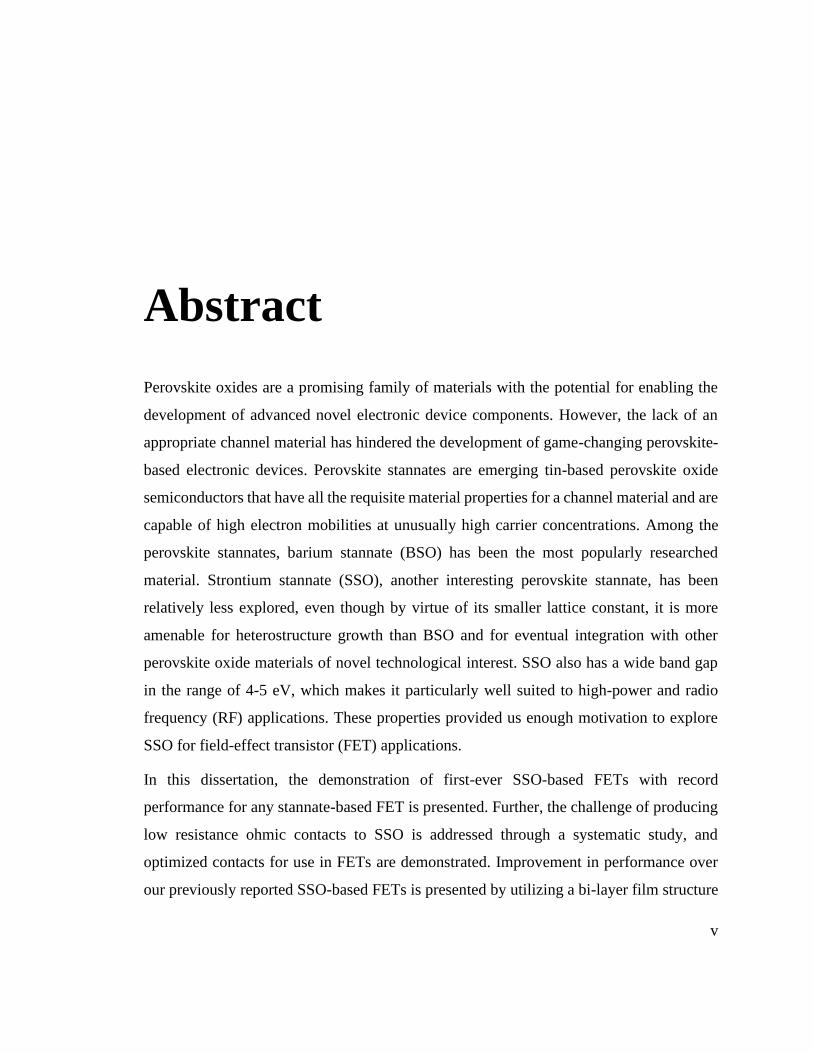
characteristic low electron in these materials, is discussed here. The main reason for the
low mobilities in the titanate-, tantalate-, and manganite-semiconductors is that the
conduction bands, derived predominantly from the d-orbitals of their respective B-site
atoms, are relatively less dispersive resulting in heavy electron effective masses in these
semiconductors [23, 24, 25]. Figure 1.3, adapted from [26], shows the band structure of
STO, where a less-dispersive conduction band similar to that of other titanate-, tantalate-,
and manganite-semiconductors, can be seen. A low maximum Hall mobility, Hall of 30
cm2/Vs for electrons was observed in tantalates (KTaO3) at room temperature [23], while
those observed in titanates (STO) and manganites (CaMnO3–δ) were lower than 10 cm2/Vs
[24, 25]. The field-effect mobilities, FE, in the channels based on the three materials [9,
10, 13, 14, 18, 19, 20] can be at least an order of magnitude lower than their Hall.
Obviously, these semiconductors are not promising as channel materials in practical
transistor applications.
The search for an appropriate perovskite oxide channel material led to rediscovery of
perovskite stannates [27, 28], which are tin- or Sn-based perovskite oxides, where Sn
occupies the B-site. The potential of stannates as channel materials remained dormant until
then due to poor material quality of previously measured stannate films [29, 30]. The next
section focusses on their superior material properties which motivated me to study
perovskite stannates as a part of my dissertation work.
FIGURE 1.3. A calculated band structure for SrTiO3 showing the relatively lesser
dispersion near the conduction band minimum (Γ). Figure adapted from [26].
9
1.2 Perovskite Stannates
A key experimental result observed in bulk barium stannate (BaSnO3 or BSO) crystals
[27], where a maximum room-temperature Hall = 320 cm2/Vs was measured for electrons
at a relatively-high electron concentration of 8 × 1019 cm-3, triggered an interest in
perovskite stannates, including BSO, strontium stannate (SrSnO3 or SSO), and calcium
stannate (CaSnO3) as a semiconductors capable of high-conductivity. The corresponding
= 70 cm2/Vs observed in an unoptimized crystalline BSO thin film [28] had suggested
that the can be improved with future structural improvements as well as optimized growth
methods, and that stannates may potentially help translate the functional diversity observed
in perovskite oxides into practical transistor structures.
The chief distinctive feature in stannates, which helps in achieving such mobilities, are
their Sn 5s-derived conduction bands, which are generally more preferable as opposed to
d-derived bands because of their high-dispersive nature that produces low-effective masses
[28, 32] (The band structures of BSO and SSO are shown in later sections.). Moreover,
relatively-high dielectric constants are also observed in these materials which helps screen
the carriers from charged-dopant atoms that can otherwise act as scattering centers. This
permits higher values at relatively-high carrier concentrations in the stannates. Stannates
tend to have band gaps wider than ~3 eV, where the band gap increases as the cation size
reduces from Ba → Sr → Ca [31]. This, when coupled with the high and high carrier
concentrations, makes them an interesting material system for applications, including
transparent conductive electrodes, transparent thin film transistors, extreme-temperature
electronics, UV-blind electronics, high-power, and radio-frequency (RF) transistors. One
important requirement is having the ideal Sn-O-Sn bonding-angle close to 180º, in order to
preserve the dispersive nature of the conduction bands [28, 32]. Additionally, the Sn-atom
may also occupy the A- site as mentioned in the previous section, which if not avoided or
minimized, can significantly compromise the stoichiometric and crystalline quality of the
material. Meeting these two requirements and ensuring overall structural as well as
stoichiometric integrity can be non-trivial and highly dependent on the growth technique

10
and conditions. This leads to a discussion on the material growth techniques for stannates
in the following section.
1.2.1 Material Growth
in BSO thin films grown using pulsed laser deposition methods were encouraging but
was still limited by defects, including grain boundaries, point defects, and dislocations [28,
31] that may be formed during the growth process due to the presence of unavoidable high-
energetic particles in the growth chambers. Molecular-beam epitaxy (MBE) can help
overcome these defects because of its inherent advantages. MBE can help grow robust-
quality films that are required for electronic device applications and is a particularly
valuable technique to grow oxide thin films [33]. The growth of an MBE film involves a
controlled reaction, where atomic or molecular species that travel in the form of beams to
react at a crystalline surface (substrate or wafer) in ultra-high vacuum conditions. The
relative concentrations of the individual reacting species can be adjusted by regulating the
flux or beam equivalent pressures (BEPs) of the respective species, providing a way to
control the stoichiometry of the films being grown. A direct benefit of the clean ultra-high
vacuum environment is the absence of high-energetic species which enables a low-energy
and controlled growth with minimized defect density [33], apart from ensuring that the
growth chamber is free from contaminant species. Other notable advantages of MBE
include epitaxial growth, in situ characterization during growth, and capability to engineer
precise heterostructure interfaces at the atomic level.
Conventional oxide MBE growth techniques involve the supply of cation film constituents
via effusion cells consisting of solid high-purity elemental sources, while the oxygen is
normally supplied via an oxygen plasma source, molecular oxygen vapor source, or even
ozone. However, such techniques can fall short of producing phase-pure stoichiometric
films in certain oxides, where some metal atoms, including Sn, Co, and Ni, display
significantly weaker tendency to oxidize [34]. This problem can be amplified in the case
of ternary oxides of the form ABO3, where the A-cation, such as Ba or Sr can have
significantly different oxidation potentials as compared to say, Sn, Co, or Ni, which are to
be restricted to the B-site only [34]. The precursors and environmental conditions in the

11
growth of such films have to be meticulously determined in order to ensure good-quality
MBE-films. Two different research groups were the first to independently demonstrate two
distinct modified-MBE methods to address this issue for the growth of stannate films. One
approach, also referred to as the radical-based hybrid-MBE involves the use of a chemical
precursor, hexamethylditin, (CH3)6Sn2 (HMDT) as the source of reactive Sn-radical during
the growth, in order to make the Sn-O reaction thermodynamically favorable [34]. The
other approach addresses the issue by sourcing high-purity solid SnO2 via an effusion cell
that can act as additional oxygen source apart from an RF O2 plasma source and together
help maintain the stoichiometry in the as-grown films [35]. Both the approaches were
successful in demonstration of conducting-BSO thin films with excellent control over
dopant concentration [35, 36] and a brief contrast of the experimental results obtained by
the two methods is discussed in the following paragraphs.
The radical-based hybrid-MBE technique was pioneered by Prof. Bharat Jalan’s research
group belonging to the Department of Chemical Engineering and Material Science at the
University of Minnesota, Twin Cities. A schematic of the hybrid-MBE chamber used by
the Jalan MBE lab is shown in Figure 1.4 which illustrates the Ba effusion cell, an O2 RF
FIGURE 1.4. A schematic of a hybrid molecular beam epitaxy (MBE) chamber and its
various components. Sn precursor is supplied via a gas bubbler system, O2 precursor
via an RF plasma, and other cation or dopant precursors can be supplied using an
effusion cell. Figure adapted from [36].

12
plasma source, and the HMDT precursor source. Additional sources such as a La effusion
cell may also be used in order to dope the stannate films. The atomic and molecular beams
travelling from the individual sources to a heated substrate wafer is also depicted to help
understand the MBE-growth concept. The MBE chamber used in the other approach with
SnO2 as a precursor can be imagined to be very similar with an additional effusion cell for
the Sn-precursor.
Using both the distinct approaches [36, 37] an adsorption-controlled growth regime was
achieved in which, the film composition is locally self-regulated because of the volatility
of the surplus growth constituents. The stoichiometry of the films is regulated by
controlling the relative BEPs of the various precursors as stated previously. Using the
hybrid-MBE approach and a Sr effusion cell instead of Ba, successful growth of conductive
doped-SSO thin films has also been shown with a maximum room-temperature
= 70 cm2/Vs [38, 39] and remains the only experimental demonstration of conductive
MBE-grown SSO thin films to date. The only other MBE-grown SSO thin films which
were obtained using SnO2 as precursor [40] were insulating for unknown reasons.
However, it is interesting to note that the same approach led to the display of a maximum
= 180 cm2/Vs in BSO thin films reported to date [35, 37], slightly larger than that of 120
cm2/Vs reported using the hybrid-MBE approach [41]. Both the approaches seem viable to
obtain stannate thin films for semiconducting device applications with room for
improvement through further optimizations. The hybrid-MBE method is perhaps a more
versatile technique that may be extended to grow other types of epitaxial films where a
compound source equivalent of SnO2 may not be easily available for use in the MBE
effusion cells to produce reactive precursors. Regardless, the superior transport properties
observed in films obtained using both the techniques show that stannates hold promise as
perovskite oxide semiconductors suitable for electronic device applications.
1.2.2 Barium Stannate
Among the perovskite stannates, barium stannate (BaSnO3 or BSO) in particular has
invited well-deserved attention as an attractive channel material for perovskite-based
electronic devices, ever since a record room-temperature electron = 320 cm2/Vs for any

13
perovskite-based semiconductor was reported [27]. A wide band gap of ~3 eV [42] and a
high-conductivity in BSO thin films attributable to mobilities above 100 cm2/Vs at carrier
concentrations exceeding 1020 cm2/Vs [35, 37, 41] already places BSO at par with the
benchmarks set by commonly used and best available transparent conducting oxides [41].
This also partly due to a relatively-high dielectric constant of 15-17 [43] in BSO. The above
properties make it an interesting channel material candidate for applications, including
transparent conductive electrodes and transparent electronics, high-power and RF
electronics, high-density quantum-well structures apart from the potential multi-functional
perovskite-based novel devices as stated before. BSO, even in its thin film form, was found
to be extremely thermally stable up to temperatures in excess of 500 ºC [27] with only
minimal degradation in transport properties suggesting possible use in extreme
environment electronics and sensors. In less than a decade since its rediscovery [27, 28], a
number of research avenues have opened up [31], based upon which one can argue that
BSO has begun to displace STO as the archetypal perovskite semiconductor and is certainly
the most-studied perovskite stannate. A discussion on any stannate materials without
discussing BSO is simply unthinkable.
1.2.2.1 Crystal and Band Structures
BSO adapts to an ideal cubic perovskite crystal structure as shown in Figure 1.5(a), where
the positions of A- (Ba), B- (Sn), and C- (O) sites are shown within a unit cell. Figure
1.5(b) also shows a BSO crystal with multiple unit cells highlighting the shared SnO6
octahedron network and the Sn-O-Sn bond angle formed as a result. The lattice constant of
the bulk cubic BSO crystal is a = 4.116 Å, slightly larger than those of commercially
available perovskite substrates. As a result, the as-grown BSO films are generally not
lattice matched to these substrates, with the mismatches ranging from the lowest of +2.3%
that was demonstrated on PrScO3 substrates to +5.1% on SrTiO3 substrates [35, 37, 41].
This mismatch generally results in misfit dislocations and strain relaxation in the films that
tend to be concentrated near the film-substrate interface in thin films, and additionally
causes threading dislocations in thicker films that can propagate through the entire

14
thickness of the films. The BSO films grown on these substrates also tend to be
compressively strained single-phase films because of the larger lattice constant of BSO
relative to the substrates.
FIGURE 1.6. Calculated band structure of BaSnO3 showing a dispersive conduction
band minimum that results in a low effective mass. Indirect band gap of ~3 eV is also
shown (Γ and R). Figure adapted from [44].
FIGURE 1.5(a) A simple unit cell of a BaSnO3 (BSO) crystal. SnO6 bonds are
represented by the octahedron. (b) An alternate representation of the BSO crystal which
shows the shared octahedral network and the perfect cubic lattice arrangement.

15
The band structure of BSO obtained using ab initio calculations by the authors in [44] is
shown in Figure 1.6. Figure 1.6 reveals a conduction band minimum at the Γ point and a
valence band maximum at the R point in the reciprocal space that corresponds to an indirect
band gap of ~3 eV, which was confirmed experimentally as well in [44]. The dispersion in
the E-k curves of the conduction band near the minimum, derived predominantly from the
Sn-5s bands as stated earlier, can also be seen in the Figure 1.6. While theoretically
calculated values of effective masses vary in the literature, recent results supported by
experiments seem to indicate a relatively-low electron effective mass of ~0.2me [32, 44,
45, 46], where me is the electron rest mass.
1.2.2.2 Mobility
The carrier is a fundamental material property that impacts the operation speed and
currents in all electronic devices. Owing to its light electron effective mass and low phonon
FIGURE 1.7. Log-log plot of the Hall measured at 300 K vs carrier concentration that
compares the Hall of BaSnO3 with that of other transparent conducting oxides and
conventional semiconductors. Figure adapted from [31].

16
scattering compared to other polar oxides, BSO is a high mobility material. The distinctive
feature of BSO, as highlighted in Figure 1.7, is that it is capable of such high mobilities
even at carrier concentrations close to 1020 cm-3, a property that is not commonly observed
in other conventional semiconductors as well as transparent conductive oxides. This can
be attributed to a combination of stronger dielectric screening [43] of the electrons from
various charged-impurity scatterers and low electron-phonon scattering in comparison to
other polar-materials [46]. Figure 1.7 shows that at comparable carrier concentrations, BSO
has higher than all the commonly used transparent conducting oxides and most other
semiconductors, except GaAs. A comparison of BSO with STO is also presented in Figure
1.7 showing a 30× higher .
Figure 1.8 displays the effect of changes in threading dislocation densities on the mobility
in BSO films, shown as a function of three-dimensional carrier concentration, n3D. To
FIGURE 1.8. Semi-log plot of the measured mobility in BaSnO3 vs n3D cm-3, plotted as
a function of different dislocation densities. Figure adapted from [41].

17
obtain the data in this figure, the authors in [41] assumed that the dislocations which can
arise due to lattice mismatch with the substrates are negative (acceptor-like) charged
scatterers. Ab initio calculations were then used to fit the experimentally measured mobility
vs n3D curves with the dislocation density as a fitting parameter. Figure 1.8 suggests that a
high dislocation density in BSO films can degrade the carrier and dislocation densities
on the order of 1012 cm-2 were estimated in these BSO films. The expected as a function
of n3D is also shown for the case of no dislocations, demonstrating a path forward to
improve the in these films. The inset in Figure 1.8 also shows that the electron-phonon
scattering limits the maximum room-temperature achievable at lower n3D.
Figure 1.9, obtained from [47], compares the data in BSO thin films and bulk crystals
obtained by various research groups showing the consistent high mobilities measured for
carrier concentrations ranging from ~2 × 1019 cm-3 to ~4 × 1020 cm-3. For very high carrier
concentrations above 5 × 1020 cm-3 the degrades steadily with increasing carrier
concentration as the impurity scattering due to dopant atoms begins to manifest in a
FIGURE 1.9. Log-log plot of the cm2/Vs, in bulk and BaSnO3 thin films vs carrier
concentration. Figure adapted from [47].
18
significant way. Another noteworthy observation is that Paik et al. [37] were able to
measure significantly higher mobilities at lower carrier concentrations in the range of 1019
cm-3 to 1018 cm-3, which they attribute to superior stoichiometric control in their growth
process, leading to a lower shear and point defects that can otherwise act as trap centers for
the carriers. This not only allowed them to measure these relatively-low carrier
concentrations but also likely improved the measured at all carrier concentrations.
Discrepancies in the data in Figures 1.8 and 1.9, despite similar dislocation densities,
suggest that the presence of point defects could be contributing to lower mobilities in the
existing BSO films. The insights provided in [37, 41] clearly indicate that higher mobilities
can be attained in BSO films by lowering the defect densities and further carefully
designing the underlying buffer (or substrate) layers as well as adjusting the growth
conditions.
1.2.3 Strontium Stannate
Strontium stannate (SrSnO3 or SSO) is another exciting semiconductor material belonging
to the perovskite stannate family. Bulk SSO stabilizes in the form of an orthorhombic
(space group: Pnma) unit cell, at room temperature, with an in-plane lattice parameter, apc
= 4.035 Å [48]. Two other crystal phases, namely orthorhombic (space group: Imma) and
tetragonal (space group: I4/mcm) are also possible with apc = 4.068 Å, and 4.069 Å
respectively, which normally exist at temperatures in excess of 905 K and 1062 K,
respectively [49]. The smaller in-plane lattice parameter for SSO with respect to BSO
(4.116 Å) not only allows better lattice matching to commercially available substrates but
makes SSO more amenable to heterostructure integration with perovskite materials of
functional and technological interest. Moreover, SSO has a wider band gap (4-5 eV) [50,
51, 52] than BSO (~ 3eV) and primarily has similar energy dispersion in the k-space, near
the conduction band minimum indicating that similar mobilities are achievable in SSO thin
films. Among the stannates, the above properties make SSO particularly well-suited to
high-power and RF electronic applications. The better lattice matching can make low
defect density growths possible, because of which SSO is perhaps well-suited even for
novel heterostructure devices.

19
1.2.3.1 Crystal and Band Structure
Figure 1.10(a) represents a unit cell of SSO that shows the Sr (A-), Sn (B-), and O (C-)
sites. As stated earlier, SSO can exist in multiple crystal phases which differ primarily in
terms of the tilting of the octahedrons in the shared three-dimensional network. Figure
1.10(b) shows the tetragonal phase structure, from which the other phases can be derived
with the help of the Glazer notation [53]. For the benefit of better visualization, the top and
front views of the SSO tetragonal phase crystal in Figure 1.10(b) are shown in Figure
1.10(c) and (d), respectively. The Glazer notation can be used to describe the different SSO
crystal phase structures with respect to the perfect cubic perovskite structure that has no
octahedral tilts (same as the BSO crystal structure). The symbol notation, a#a'#c#, where the
superscript # can take on the values 0, +, or –, can be used to indicate no tilt, adjacent
FIGURE 1.10. (a) Simple unit cell of SrSnO3 (SSO) showing the SnO6 bonds and
relative positions of the Sr atom. (b) SSO in tetragonal I4/mcm phase and the
corresponding axis directions are also shown. (c) Top view of crystal shown in (b). (d)
Front view of crystal shown in (d).

20
octahedrons tilting in the same, or opposite directions, respectively. The letters a, a', and c
refer to tilt around the [100], [010], and [001] directions of the cubic perovskite coordinate
system, respectively. Starting from a0a'0c0, which is the perfect cubic perovskite structure,
the I4/mcm tetragonal phase in Figure 1.10(b) can be obtained with a0a'0c– tilting [49]. The
orthorhombic Pnma and Imma phases can be obtained using a–a'–c+ and a–a'–c0 tilts,
respectively [53]. The smaller size of the Sr cation in comparison to the Ba cation allows
these octahedral tilts and thus, multiple crystal structures to exist. Even though the I4/mcm
tetragonal and Imma orthorhombic phases normally do not exist at room temperatures, it
has been shown that all the three phases can be stabilized on different substrates using
strain engineering and hybrid-MBE growth method [54].
While no significant change in the band gap is expected in the three phases [55, 56], it has
been shown experimentally and supported via theoretical calculations that the I4/mcm
tetragonal phase is capable of a higher than the orthorhombic Pnma phase [54]. In fact,
the experiments showed a 3-fold increase in the I4/mcm tetragonal phase films even
though the dopant concentration was kept the same as that of the orthorhombic Pnma phase
films, suggesting that other factors such as defect- or phonon-scattering may be further
reducing the in the orthorhombic Pnma phase films. Figure 1.11(a), obtained from [55],
FIGURE 1.11. (a) Calculated band structure for tetragonal I4/mcm SrSnO3 (SSO). (b)
Dispersion around the conduction band minima for the tetragonal and orthorhombic
phases are shown which shows a lower effective mass for electrons in the tetragonal
phase of SSO. (a) and (b) adapted from [55] and [54], respectively.

21
shows the calculated band structure for the I4/mcm tetragonal phase, where the dispersive
conduction band minimum can be seen. Figure 1.11(b), obtained from [54], compares the
two-dimensional projection of E-k surface of the I4/mcm tetragonal and orthorhombic
Pnma phases to show that the electron effective mass is smaller in the I4/mcm tetragonal
phase. The effective mass of electrons in the I4/mcm tetragonal phase was found to be
~0.3me which is comparable to that of the BSO effective mass indicating that similar
values can be obtained in SSO films as well. However, other factors such as phonon-
scattering that can vary from phase to phase may also come into play which can affect the
mobilities attainable in SSO. As a final note on the band structure, even though Figure
1.11(a) suggests a smaller band gap obtained from theoretical calculations, other
experimental and band gap calculations that have accounted for strain in the SSO films
strongly suggest a band gap in the range of 4-5 eV [50, 51, 52, 54, 55].
1.2.3.2 Mobility and Surface Effects
The tetragonal-phase stabilized SSO films grown on GdScO3 (110) [39, 54] using the
hybrid-MBE approach were shown to have good mobilities with a record reported value of
70 cm2/Vs for any SSO film [38, 39, 50, 52, 54, 56]. These films [38, 39, 54] happen to be
the only MBE-grown conductive-SSO films reported to date. Figure 1.12 shows the
dependence of mobility and n3D on the La-effusion cell temperature, TLa, (equivalent to La-
doping concentration). The record value of 70 cm2/Vs was observed, much like in BSO,
at a high n3D of 1.1 × 1020 cm-3. At even higher dopant concentrations surpassing the La-
FIGURE 1.12. n3D and Hall mobility in SrSnO3 plotted vs TLa Figure adapted from [39].

22
solubility limit, charge compensation can occur [57], and the begins to drop due to
increased scattering. A decrease in the value with decreasing n3D as in BSO is observed
here as well. In BSO thin films, this was attributed to dislocations induced by lattice
mismatch between BSO and the substrate. However, in the SSO films which are better
lattice matched threading dislocations should be significantly lower and other charged-
impurity disorder sources are suspected to cause the observed reduction in [39, 54]. A
detailed study on the defects and disorder in SSO thin films is lacking which is needed to
understand the means to improve the in SSO thin films.
n3D lower than 1019 cm-3 in SSO thin films could not be measured because of an undesirable
surface depletion in the films [39]. This surface depletion may also exist in films with
higher n3D as well and can have adverse effects on devices fabricated on such films as
explained in later chapters. Such surface effects have also been observed in other oxide
semiconductors as well [58, 59, 60] but is more pronounced in SSO possibly due to its
larger dielectric constant [43, 61]. Surface depletion widths greater than 3 nm have been
estimated in SSO thin films. As a result, when determining three-dimensional (3D) carrier
densities using the measured two-dimensional sheet carrier densities, one must note that
the true 3D carrier densities may be different depending on the surface depletion in the
films [39].
1.3 Early Perovskite Oxide Device Results
Early perovskite-based FETs were based on low room-temperature−mobility materials,
including STO and KTaO3 [13, 14, 21, 62-66]. The measured FE in these devices were
less than 5 cm2/Vs and the mobilities were low even in high-charge density two-
dimensional electron gas-based heterostructures, negating the advantage offered by the
ability to modulate a large carrier density in the channels [13, 14]. Apart from a low-
mobility, oxygen vacancies can also be a cause of concern in STO-based devices [13, 63,
66]. Since the emergence of BSO as a high-mobility material [27], much of the work has
been focused on BSO-based FETs [31, 67-70]. In Table 1.2, key early perovskite oxide-
based transistor results [13, 14, 21, 31, 62-70] are recorded, where the FE, gate length, LG,

23
transconductance, gm, the band gap of the semiconducting channel are listed. The maximum
FE in a BSO-based FET was ~20× of those observed in any STO-based device. The FE
observed in all the BSO FETs with different configurations were in fact higher than in any
TABLE 1.2. Comparison of early perovskite oxide-based FET results.
0.01 0.1 1 10 100 100010-3
10-1
101
103
KTO
STO (heterostructures)
STO
BSO-
BSO
Drive C
urr
ent, I
DS
AT (
mA
/mm
)
Gate Length, LG (m)
FIGURE 1.13. Drive current obtained from reports of early perovskite oxide FETs [13,
14, 21, 31, 62-70] plotted vs gate length.

24
other perovskite oxide material. Consequently, the gm values in BSO FETs at a comparable
LG are also higher, as can be inferred from Table 1.2.
Figure 1.13 plots the maximum drive currents, IDSAT, in the devices with different channel
materials [13, 14, 21, 31, 62-70] vs LG. The high-charge densities in [13, 14] and the small
LG in [65] allow these devices achieve drive currents in excess of 100 mA/mm. While the
drive currents in the BSO-based devices are lower in comparison mainly due to their large
LG, significantly large currents can be achieved in these devices by optimizing the device
dimensions. The encouraging early BSO device results indicate huge potential for stannates
as semiconducting channel materials. Early stannate-based FETS were based entirely on
BSO and there were no SSO-based FET results reported to my knowledge before this work.
Apart from one initial report [50], the potential for SSO as a channel material remained
latent until the report of hybrid-MBE grown SSO thin films with conveniently controllable
doping and moderately high mobilities [38, 54].
1.4 Dissertation Goal
Higher performance requirements have been projected for the electronics that are to drive
the future high-speed communication ecosystems. This has compelled researchers to study
a newer class of ultra-wide gap (UWG) materials with band gaps wider than that of GaN
and SiC, which enable the existing RF-integrated circuits (RFICs) that form the basis of
such communication systems.
The preceding sections elucidated the unparalleled edge offered by the multi-functional
perovskite oxide system towards development of novel electronic devices. The evaluation
of hetero-oxide interfaces for novel functional devices is still a nascent research field but
one with vast potential. The unearthing of stannates as high-mobility wide gap
semiconductors opens up avenues for researchers to tap the enormous multitude of
interesting physical properties within the perovskite oxide family via heterostructure
engineering. Among the stannates, BSO is certainly an exciting material with potential for
use in several electronic and optoelectronic applications but SSO is perhaps more
interesting for high-power and RFIC applications because of its wider band gap (> 4 eV).
SSO can be an exciting addition to the emerging UWG-materials-class as it can potentially

25
have large intrinsic breakdown fields that are essential for such applications. Besides, the
smaller lattice constant in SSO can be beneficial for heterostructure growth which can help
produce high-current and high-speed transistors. Higher mobilities similar to those that
have already been demonstrated in BSO thin films can be achieved in SSO as well.
One of the key insights that I have learned from my research so far is that while exploring
novel materials for future electronic applications, one needs to look beyond just their
suitability for current needs and instead envision what new applications could eventually
be realized. While there are several emerging UWG materials, the distinct advantages
enumerated in the earlier discussions make SSO stand out as a uniquely interesting material
for next-generation RFICs, and this material is the focus of my dissertation research. As
one of the first few device researchers working on SSO thin films, my goal is to overcome
the challenges of working with new materials to develop processing methodologies,
understand the material properties, experimentally demonstrate the suitability of SSO for
FET applications, and lay the foundation for development of next-generation devices using
the perovskite family.
26
Chapter 2
Single-Layer MESFET
Results
27
This chapter reviews the results obtained from transistors fabricated on strontium stannate
(SrSnO3 or SSO) thin films grown using hybrid-MBE. All the films used during the course
of my dissertation research were grown by the Jalan MBE lab, Department of Chemical
Engineering and Materials Science, University of Minnesota, Twin Cities. Working with a
new material can involve many challenges as many of the material properties are simply
unknown. In the initial phase, I used Sentaurus technology computer-aided design (TCAD)
simulations to determine the design specifications and then worked on developing
fabrication recipes that led to the demonstration of a first-ever SSO-based FET. The details
are presented below.
2.1 MESFET
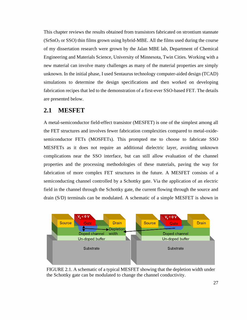
A metal-semiconductor field-effect transistor (MESFET) is one of the simplest among all
the FET structures and involves fewer fabrication complexities compared to metal-oxide-
semiconductor FETs (MOSFETs). This prompted me to choose to fabricate SSO
MESFETs as it does not require an additional dielectric layer, avoiding unknown
complications near the SSO interface, but can still allow evaluation of the channel
properties and the processing methodologies of these materials, paving the way for
fabrication of more complex FET structures in the future. A MESFET consists of a
semiconducting channel controlled by a Schottky gate. Via the application of an electric
field in the channel through the Schottky gate, the current flowing through the source and
drain (S/D) terminals can be modulated. A schematic of a simple MESFET is shown in
FIGURE 2.1. A schematic of a typical MESFET showing that the depletion width under
the Schottky gate can be modulated to change the channel conductivity.

28
Figure 2.1 highlighting the Schottky gate contact and the S/D Ohmic contacts. Figure 2.1
also shows the change in the effective channel thickness as the depletion region varies with
applied gate voltage. In a MESFET, the depletion region created by the semiconductor-
Schottky gate interface separates the carrier away from the surface, which can reduce the
scattering time of the carriers, resulting in higher field-effect mobility, 𝜇𝐹𝐸, in the MESFET
as an added advantage.
2.2 Sentaurus TCAD Simulation
The key design parameters in a MESFET are the doping and the thickness of the channel.
As shown in Figure 2.1 the depletion region can be modulated with an applied gate voltage
and for a given applied gate voltage, known as the threshold voltage, the channel is
completely pinched off. The channel doping and thickness are co-dependent parameters
that can be tuned in order to produce an optimal combination that maximizes the drive
current while still being able to pinchoff the channel. This was the primary goal of my
simulation.
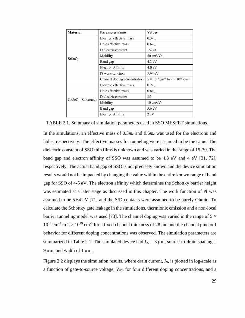
The parameters used in the simulations were determined based on discussions with Jalan
MBE lab members, Abhinav Prakash, Tristan K. Truttmann, and Fengdeng Liu. In a
Schottky junction, for a n3D > ~1018 cm-3, the tunneling leakage current increases
exponentially with increasing current [71]. High gate leakage currents are generally
unfavorable in a transistor and are detrimental to the device behavior. As a result, n3D >>
1019 cm-3 are generally avoided in MESFET designs. In films with moderate thicknesses
and n3D << 1019 cm-3, surface depletion effects which were described in the earlier chapter,
tend to make the films very resistive. Very thick films (> 80 nm) were avoided for reasons
beyond the scope of this discussion. Based on the discussions with Jalan MBE lab members
and their experience from initial success in the growth of SSO films with good quality,
films with an n3D close to ~1019 cm-3 were targeted, and the thickness was kept fixed at ~28
nm. At this thickness, the SSO films grown on GdScO3 (110) tend to be dominantly
tetragonal in phase which is favorable for transistors because of the smaller electron
effective mass in the films with this phase.
29
In the simulations, an effective mass of 0.3me and 0.6me was used for the electrons and
holes, respectively. The effective masses for tunneling were assumed to be the same. The
dielectric constant of SSO thin films is unknown and was varied in the range of 15-30. The
band gap and electron affinity of SSO was assumed to be 4.3 eV and 4 eV [31, 72],
respectively. The actual band gap of SSO is not precisely known and the device simulation
results would not be impacted by changing the value within the entire known range of band
gap for SSO of 4-5 eV. The electron affinity which determines the Schottky barrier height
was estimated at a later stage as discussed in this chapter. The work function of Pt was
assumed to be 5.64 eV [71] and the S/D contacts were assumed to be purely Ohmic. To
calculate the Schottky gate leakage in the simulations, thermionic emission and a non-local
barrier tunneling model was used [73]. The channel doping was varied in the range of 5 ×
1018 cm-3 to 2 × 1019 cm-3 for a fixed channel thickness of 28 nm and the channel pinchoff
behavior for different doping concentrations was observed. The simulation parameters are
summarized in Table 2.1. The simulated device had LG = 3 m, source-to-drain spacing =
9 m, and width of 1 m.
Figure 2.2 displays the simulation results, where drain current, ID, is plotted in log-scale as
a function of gate-to-source voltage, VGS, for four different doping concentrations, and a
TABLE 2.1. Summary of simulation parameters used in SSO MESFET simulations.

30
drain-to-source voltage of 5 V.. As can be seen from Figure 2.2, the gate leakage current
due to tunneling, dominates the off state ID for doping greater than 2 × 1019 cm-3. For a
channel doping of 5 × 1018 cm-3, the ID in the off state is close to the thermionic emission
limit with no appreciable tunneling current, but this is not an optimal doping for this
thickness as the drive current in the on state is too low. Based on these results, an n3D in the
range of 1 × 1019 cm-3 to 1.5 × 1019 cm-3 was targeted during growth for this experiment.
2.3 Device Fabrication
The device fabrication sequence started with using radical-based hybrid-MBE to grow
epitaxial SSO thin films on a 5 mm × 5 mm, semi-insulating GdScO3 (110) substrate that
was commercially purchased. The growth was performed by Abhinav Prakash and Jin Yue
from the Jalan MBE lab. SSO is -1.6% lattice mismatched to the substrate GdScO3, which
provides a pseudocubic (001)pc perovskite template for the epitaxial growth of SSO. The
substrate was heated to a thermocouple temperature 950 in an MBE chamber with a
background of 10-10 Torr. The substrate was then cleaned using a 250 W RF O2 plasma
which is also used as the precursor source for O2 later during the growth. The precursors,
Sr and La were supplied via thermal evaporation from an effusion cell, Sn was supplied
via the chemical precursor hexamethylditin (HMDT). The details of the growth technique
-5 -4 -3 -2 -1 0 110-9
10-6
10-3
100
103D
rain
Cu
rre
nt (m
A/m
m)
Gate-to-Source Votlage (V)
5e18 cm-3
1e19 cm-3
1.5e19 cm-3
2e19 cm-3
FIGURE 2.2. Simulated transfer characteristics of a MESFET with SSO channel
thickness of 28 nm and four different values of channel doping. LG = 3 m, source-to-
drain spacing = 9 m. Drain-to-source voltage = 5 V.

31
are explained elsewhere [34, 38, 54]. As explained in the previous chapter, using this
hybrid-MBE approach an adsorption-controlled growth regime can be achieved with
scalable growth rates and atomically smooth film surfaces [36]. Along these lines, using
beam equivalent pressures of 3 × 10⁻⁸ Torr for Sr, 2.4 × 10⁻⁶ Torr for HMDT, and
5 × 10⁻⁶ Torr for O2 (RF plasma) a stoichiometric condition was achieved for the growth.
La was used as an n-type dopant and its concentration in the channel layer was fixed by
keeping the effusion cell temperature, TLa = 1125 °C. Using these conditions, a thin 11 nm
near-intrinsically-doped (NID) buffer layer was first grown on the substrate without
providing any La precursor. Then, a 28 nm La:SSO film was grown as the active channel
layer. Figure 2.3(a) shows a schematic representation of the as-grown SSO layers on the
substrate. From van der Pauw measurements, the as-grown films were known to have an
n3D = 2.3 × 1019 cm-3, sheet resistance, Rs = 1.9 kΩ/, and Hall = 50 cm2/Vs. The carrier
concentration was calculated assuming the effective thickness of the film to be the same as
that of the doped-film thickness = 28 nm, and the actual carrier concentration could be
higher as this value does not account for surface depletion which changes the effective
thickness of the film.
FIGURE 2.3. Fabrication sequence of a MESFET showing (a) as grown film, (b) mesa
isolation step, (c) Ohmic contacts deposition, and (d) Schottky gate deposition.

32
The reminder of the fabrication sequence, which is shown in Figure 2.3, was performed in
the Minnesota Nano Center. As shown in Figure 2.3(a)-(d), after the growth, regions
outside of the mesa patterns are first etched away to isolate the devices, then source and
drain ohmic contacts were deposited, and finally the gate metal was evaporated and lifted
off to complete the device structure. The essential details of the process and each of the
fabrication steps are discussed below.
2.3.1 Photolithography Process and Alignment Marks
Hard contact exposure was used to perform photolithography in all my fabrications to help
achieve features with tight tolerance. A dynamic-dispense spin coating technique was used
to form a near-uniform photoresist layer on the substrate. In the dynamic-dispense spin
coating process, the substrate, which is attached to the spin chuck via vacuum, was set to
spin at a speed of 5000 rpm prior to dispensing the resist. Then using a pipette, one drop
of AZ® 1512 photoresist was dispensed close to the center of the substrate and the
photoresist solvent was subsequently allowed to evaporate by continuing to spin the
substrate for 45 s. The standard static-dispense spin coating process, where the photoresist
is dispensed before starting the spinning, was avoided as it results in a prominent edge bead
because of the small size and square shape of the substrates. The edge bead, if not avoided,
interferes with the contact exposure process and results in poorly exposed features. For
FIGURE 2.4. Optical micrographs of substrates obtained after develop and exposure on
a resist film obtained using (a) static dispense spin coating (b) dynamic dispense spin
coating techniques, respectively. Same develop time (3.5 min) was used in both cases.
The small square features are ~10 × 10 m2.

33
comparison, features obtained after exposure with the same mask using the two different
coating techniques are shown in Figure 2.4. Because of a significant edge bead resulting
from the static-dispense coating, the features that were supposed to be sharp and rectilinear
were blurred and rounded. Owing to the small size and square shape a small edge bead was
still present even after dynamic spin coating, because of which the corner features,
particularly in patterns away from the center of the sample, were not perfectly sharp even
though the features were significantly less rounded in comparison with those obtained
using the static coating technique. This edge bead can be removed, if needed, using bead-
removal lithography step before pattering in future. For all the photolithography steps, the
dynamic-dispense spin coating process described above was used along with a hard contact
exposure of 5 s. In order to better clear the resist in the corners despite the slight edge bead,
5.5 s exposure was used in all the subsequent experiments apart from the current one being
described. Post-exposure, the features were developed for 30 s in a MF® 351 developer. In
photolithography steps where an image reversal of the exposed patterns was performed,
the features were developed for 3.5 min using the same developer, after an additional
exposure for 8 min under a UV light source.
Since the film and the substrate are transparent, reflective alignment marks were first
formed on the substrate in order to be able to align the subsequent layers with each other.
For this, after patterning the mark features using photolithography, a Ti (10 nm) / Al (50
nm) metal stack was evaporated and lifted off to form the alignment marks on the substrate.
2.3.2 Mesa Isolation
A wet-etch process was developed to perform the mesa isolation. After initial room
temperature trials using hydrochloric acid (HCl) with concentrations ≤ 1M produced no
measurable etch depths, etch experiments were performed using 1M HCl heated to 60
using a hot plate. The solution was allowed to rest on the hot plate for 30 min before starting
any etching in order to stabilize the actual solution temperature. For the purpose of
performing etch experiments a sample with similar doping concentrations (TLa = 1150 )
was used. These trials produced an etch rate of ~16.8 nm/min which was calibrated using
linear fitting of the data shown in Figure 2.5(a). Short etches produced a sharp edge profile

34
as can be seen from the AFM graphs in Fig. 2.5(b), which corresponds to an etch of 30 s.
If the etching was performed for relatively longer durations, due to isotropic etch and
possible resist wicking near the pattern edges, a tapered edge profile was observed in both
profilometer and AFM scans which are shown in Fig. 2.5(c) and (d), respectively. The data
in 2.5(c) and (d) correspond to an etch duration of 2.5 min. In the actual sample, the mesa
patterns were generated using photolithography and the isolation was performed using a
combination of the above described wet etch and dry etch in an Ar plasma for 1.5 min and
10 min, respectively. The total etch depth after this process was measured to be ~47 nm.
2.3.3 Schottky and Ohmic Contacts
The source and drain (S/D) features were patterned and Sc (10 nm) / Au (80 nm) was
deposited using electron-beam evaporation to form the S/D contacts. Then, gate features
were patterned next using photolithography and Pt (10 nm) / Ti (10 nm) / Al (80 nm) / Ti
FIGURE 2.5. (a) Etch rate for SSO using 1M HCl at 60 ºC. (b) AFM height map after
SSO 30 s etch in HCl. (c) Profilometer scan results after 2.5 min etch in HCl. (d) AFM
height map after 2.5 min etch in HCl.

35
(10 nm) was evaporated to form the Pt Schottky gates. An O2 RF plasma (50 W and 100
sccm O2 flow) clean was performed for 30 s in both the gate and contact deposition steps
just before the metals were evaporated in order to remove any organic residue remaining
after the resist development. The evaporation was performed under vacuum conditions and
it was ensured that the chamber pressure was always below 1.3 × 10 6 Torr for the entire
duration of the deposition.
2.4 Device Measurement Results
All the measurements were obtained at room temperature using a Keysight B1500
semiconductor parameter analyzer.
2.4.1 Transfer-Length Method Results
FIGURE 2.6. (a) Optical micrograph of a TLM structure with different contact spacings.
(b) Current vs voltage curves of Sc contacts measured at room temperature before
annealing. (c) Current vs voltage curves of Sc contacts after 300 ºC annealing. (d)
Contact and sheet resistance extraction from the TLM data. Contact spacings of 4, 6, 8,
10, and 15 m were used.
36
A picture of the fabricated transfer length structure is shown in Figure 2.6(a). Despite, the
low-work function (~3.7 eV) of Sc metal, the contacts were found to be Schottky-type and
highly resistive in nature when measured immediately after fabrication. Figure 2.6(b) plots
the current as a function of voltage applied between the contact fingers, for different
spacings between the fingers. It is suspected that the O2 plasma clean may have created
unintentional surface depletion, in addition to what may be already existing in the films,
creating an insulating barrier between the contacts and the underlying La:SSO, and
resulting in such resistive contacts.
In an attempt to improve the contacts, the substrate was then annealed in an inert Ar
atmosphere for 5 min at a thermocouple temperature of 300 inside a rapid thermal
annealing (RTA) system. The annealing improved the contact resistance by possibly
diffusing the Sc contacts and removing the barrier in between. The current-voltage curves
obtained from the same TLM structures are shown in Figure 2.6(c). As can be seen from
Figure 2.6(c), the contacts show Ohmic behavior after annealing. The resistance data
obtained as the inverse of the slope of the IV curves is plotted vs contact separation distance
in Figure 2.6(d). The contact resistance, Rc, was extracted by extrapolating the linear fit of
the resistance data plotted vs contact spacing that is shown in Figure 2.6(d). However, the
extracted Rc = 38 ± 24 Ω-mm had a large error because of the high variability in the
contacts. The large error bar caused the extracted sheet resistance, Rs = 4976 ± 5344 Ω/,
obtained as the slope of the linear fit in Figure 2.6(d), to significantly deviate from the
values obtained using van der Pauw measurements on the as-grown films.
2.4.2 MESFET Characterization
Figure 2.7(a) and (b) show the schematic and micrograph of a MESFET. The MESFET in
Figure 2.7(b) had a LG = 3 m, and a S/D spacing, LDS = 9 m. The output characteristics
of this MESFET is shown in Figure 2.8, where the ID is plotted vs drain-to-source voltage,
VDS, for different VGS ranging from -3 V to 1 V, in steps of 0.5 V. The output characteristics
of the devices are similar to that of a typical n-FET, showing good saturation and low
output conductance. The drive currents of these devices were limited by the relatively-high
S/D contact resistance. A maximum extrinsic drive current of 36 mA/mm was measured

37
for the MESFET at a VGS = +1 V and a VDS = +3.5 V. This was the first-ever demonstration
of a SSO-based FET to my knowledge.
Figure 2.9(a) shows the transfer characteristics of the same device, in which the ID is plotted
vs VGS, for a VDS = +3.5 V, a value that biases the MESFET in the saturation region of its
operation. The extrinsic transconductance, gm, of this device is also plotted in the same
chart on the right-hand side axis. From this data, the peak gm was determined to be 17
mS/mm, once again limited by the high-contact resistance, is lower than the actual or
intrinsic transconductance, gmi. The gmi can be estimated if the source resistance, RS, is
known, using the equation 2.1:
0 1 2 30
10
20
30
40
VGS = -0.5 V
Dra
in C
urr
ent (m
A/m
m)
Drain-to-Source Voltage (V)
VGS = +1 V
FIGURE 2.8. Output characteristics of a MESFET showing ID plotted vs VDS for
different values of VGS ranging from +1 V to 3 V, in steps of –0.5 V [75]. Devices had
LGS = 3 μm and LDS = 9 μm.
FIGURE 2.7. (a) Schematic of a completed MESFET. (b) Optical micrograph of a
MESFET with LGS = 3 μm and LDS = 9 μm [75].

38
𝑔𝑚𝑖 = 𝑔𝑚 (1 − 𝑔𝑚𝑅𝑆)⁄ (2.1)
The contact resistance in the devices was estimated to be 30 Ω-mm, using the output
characteristics in Figure 2.8 with the help of the known values of Rc and sheet resistance.
This resulted in an estimate for gmi = 35 mS/mm. Figure 2.9(b) shows a plot of the √ID
vs VGS, which can be used to extract the threshold voltage, VT, and the FE, based on the
equations 2.2 and 2.3 shown below, if the dielectric constant, κ, of SSO is known.
𝐼𝐷 = 𝑘𝑛(𝑉𝐺𝑆 − 𝑉𝑇)2, (2.2)
where, kn is known as the conduction parameter of the MESFET and is given by the
equation 2.3.
𝑘𝑛 = 𝜇𝐹𝐸𝜅𝜖0 2𝑎𝐿𝐺⁄ (2.3)
The kn and ID, used in the equations 2.2 and 2.3 are in units of SV-1m-1 and A/m,
respectively. The parameter, a, is the thickness of the active layer, i.e. 28 nm. Using these
relations, a linear fitting, as shown in Figure 2.9(b), was performed and a VT = -2.1 Vwas
obtained using extrapolation. This can be verified from Figure 2.9(a) where the depletion-
mode behavior is also evident. A precise value for the κ of SSO has not been measured so
far. Using a value [43, 61], in the range of 15 to 30 for the κ, the FE was found to be ranging
from 48 to 24 cm2/Vs, which is a reasonable estimate in comparison with the values
obtained from van der Pauw measurements on the as-grown film.
FIGURE 2.9. (a) Transfer characteristics of a MESFET showing ID plotted vs VGS, for
VDS = +3.5 V [75].

39
Figure 2.10 shows the transfer characteristics with ID plotted on a log scale, from which the
off current can be seen to be limited by the gate leakage current. Using the Sentaurus TCAD
simulation setup described in the previous sections, the on-state characteristics of the
device were fitted to the simulated ID, using the parameter values of n3D, and κ of SSO
as 1.6 × 1019 cm-3, 50 cm2/Vs, and 30, respectively. The comparison of the simulated and
actual off currents in Figure 2.10 indicates that the expected off current is much lower than
the actual measured current. The excess leakage current can be attributed to the annealing
of the Schottky gates at a moderately high temperature of 300 . The non-ideal approach
of annealing after the deposition of Schottky gates can be avoided in future to prevent the
excessive gate leakage. It must be noted that the simulations assume that the channel is a
uniformly doped layer and its entire thickness of 28 nm is modulated by the applied gate
voltage. In reality, the existence of surface states could be additionally depleting the
channel apart from the Schottky gate and the three-dimensional carrier concentration may
be non-uniformly varying with the depth of the channel layer. The real material parameters
would then be different from the fitted simulation parameters but should likely be in the
vicinity of the values estimated above.
In order to determine the Schottky barrier height of the Pt-SSO junction, capacitance-
voltage and current-voltage measurements were performed between the anode and cathode
FIGURE 2.10. Experimental (points) and simulated (lines) ID (blue) and IG (green)
plotted vs. VGS. The results show that the on-to-off current ratio is mainly limited by
gate leakage [75].

40
electrodes of the Schottky junction. The current-voltage characteristics shown in the inset
of Figure 2.11 were used to obtain an estimate for the series resistance, which in-turn was
used to obtain corrected capacitance, C, and diode voltage, VSchottky, values using the
method described in [74]. Using a linear extrapolation of the 1/C2 vs. VSchottky plots,
obtained at 100 kHz, a barrier height of 1.55 eV was extracted. This value is consistent
with the measured rectifying forward current characteristics of the Schottky diode. The
barrier height for Pt-SSO Schottky junction also confirms the conduction band edge
position of SSO, which can be estimated to be at ~4.1 eV. If the κ is known, these plots
offer another independent way to verify the doping concentration. Using the range of κ =
15-30 as above, a doping concentration value of 2 × 1019 cm-3 to 4 × 1019 cm-3 is estimated
from the slope of these curves, which is roughly consistent with the value obtained from
van der Pauw Hall measurements. The FE value was also estimated using the gmi and the
C data, which resulted in 16 cm2/Vs at VGS = +0.8 V to 30 cm2/Vs at VGS = -0.8 V. The
accuracy of this value is reliant on the effective area of the Schottky junction which cannot
be precisely determined. As a result, the FE extracted from equation 2.3 is likely a more
accurate estimation.
FIGURE 2.11. 1/C2 vs. VSchottky plots obtained from capacitance-voltage measurements
performed at frequencies of 50 kHz, 100 kHz, and 500 kHz. Inset: Gate current density
vs. voltage for the Schottky diode [75].

41
Finally, the performance of this FET was compared with that of the prior results on STO,
BSO, and KTaO3 FET data in Table 1.2. The performance of this FET measured in terms
of peak gm, is higher than any previously reported stannate-based FET owing to the shorter
gate length and superior quality of the hybrid-MBE grown SSO films. The peak gm of our
MESFETs is also a roughly 5× improvement over the best STO-based FET at a comparable
gate length. The peak gm values reported in [75] based on my preliminary work was a record
value for any perovskite-based FET during the time of the publication. This study also led
to estimation of first-ever experimental FE in SSO films. Despite the promising peak gm
values in the devices, the FE estimated from both methods, seems to be lower than the Hall
mobility obtained on the as-grown films. A detailed study is needed to understand the
reasons behind the same. The performance improvements demonstrated in SSO FET over
any prior perovskite-based FETs is a further evidence to the capability of stannates as
channel materials.
2.4.3 Contact and Device Degradation
Although the Sc contacts demonstrated good Ohmic behavior after deposition and
annealing, the contacts degraded in air gradually. Based on the learnings from prior
measurements performed on SSO films good long-term atmospheric stability is expected
for SSO which points to oxidation of the Sc metal as the likely reason for contact
FIGURE 2.12. (a) TLM current vs voltage curves obtained initially (solid lines)
compared to those obtained 4 weeks later (dashed). (b) Transfer characteristics
measured of the same MESFET (LGS = 3 μm and source-to-drain spacing, LDS = 9 μm)
measured over a period a time to device degradation.

42
degradation. Figure 2.12(a) shows the significantly lower currents measured on the same
TLM structures four weeks (dashed lines) after the initial measurements (solid lines) were
obtained. The transient behavior of the device discussed above is also compared with the
initial measurement in Figure 2.12(b). Here, four different measurements obtained at
different times over period seven weeks is shown. Clearly, these contacts are unstable and
require significant optimization and the contact resistance obtained in the initial
measurement was itself too high. The approach used to address these issues is discussed in
the following chapter.

43
Chapter 3
Ohmic Contact
Optimization

44
The ability to achieve low contact resistances, stable and reliable contacts are vital to any
electronic device. A high contact resistance not only prevents the ability to measure and
understand intrinsic device properties, as shown in the previous chapter, but can also lead
to higher resistive losses and excessive heat dissipation which can in turn degrade the
device performance further and can even lead to device failure. Contact resistance has, in
some cases, been identified as radio frequency (RF) performance bottlenecks in both active
and passive electronic circuit components [76, 77] limiting the achievable maximum
operational frequency and quality factor in these devices. The importance of achieving low
contact resistance cannot be understated. This chapter outlines the results of the Ohmic
contact experiments performed on SSO.
3.1 Band-Edge Work Function Metals
Several approaches have been proposed to form low-resistive Ohmic contacts to
semiconductors [71, 78-81]. The easiest approach, in theory, is the use of a contact metal
whose work function is the same as or very close to the band edge of the semiconductor,
with a band offset of under ~0.025 eV. This can result in very low contact resistances
because the active electrons (holes) that are made available by the metal, can then move
freely to and from the conduction (valence) band of the semiconductor without having to
surpass an energy barrier [71]. However, practical metal-semiconductor interfaces can be
non-ideal and due to Fermi-level pinning or simply, lack of a band-edge work function
metal can produce finite barrier heights. One alternate approach is the use of a heavily-
doped semiconductor beneath a contact metal that minimizes the effect of the energy
barrier at the metal-semiconductor junction and causes tunneling to be the dominant
conducting mechanism. In the absence of a metal that can produce a low enough barrier,
alloyed contacts with engineered work functions may also be used. Both these approaches
have been used in Si as well as in GaN, where metal-silicide alloyed contacts on heavily
implanted Si [80] and Ta, Ti, Al, or Ni-based alloys have been used on regrown GaN layers
[78, 79] to produce record low contact resistances for those materials systems. Another
unique approach was used on InP semiconducting layers, where the metal deposition was
carried out in situ immediately after the growth of the underlying film in an MBE chamber

45
avoiding exposure of the film to air. This process ensures a clean interface, free of
contaminants, prevents surface oxidation and produced low-contact resistance that helped
achieve THz operation in InP-based devices [81].
Alloyed Al-based contacts have been previously explored on perovskite oxide
semiconductors, including KTaO3 and SrTiO3 [82]. However, because they are a relatively
new material system no such contact studies exist on the stannates. This is the first study
on Ohmic contacts to any perovskite stannates, to our knowledge. In this study, we attempt
to exploit one of the key features of the stannates that was discussed in the first chapter,
viz. the capability of achieving high mobilities at a relatively-high doping level of up to
~1020 cm-3. The high doping levels and the high mobility can be exploited to produce low
contact resistance by using a low-barrier metal that can lead to tunneling band-edge
contacts. The low effective mass in the stannates can allow for high tunneling probabilities,
and thus lower contact resistance than other materials with relatively higher effective
masses.
From the study described in the previous chapter, the electron affinity or conduction band-
edge of SSO was found to be at roughly ~4.1 eV. During initial experiments, Cr contacts
were explored on an SSO thin film with thickness of 28 nm and carrier concentration of
2.3 × 1019 cm-3. These contacts were highly resistive and also Schottky type in nature as
shown in Figure 3.1. The barrier height for Cr contacts is expected to be ~0.4 eV assuming
the above electron affinity for SSO and a work function of 4.5 eV for Cr. Even though the
-0.4 -0.2 0.0 0.2 0.4-0.10
-0.05
0.00
0.05
0.10
Cu
rre
nt
(A
/mm
)
Voltage (V)
6 m
8 m
FIGURE 3.1. Current vs voltage curves obtained for Cr contacts to SSO showing high
resistivity and Schottky type behavior when measured at room temperature.

46
barrier height was not too large, these contacts conducted much smaller currents when the
as-fabricated structures were measured at room temperature, without any annealing. This
is a surprising result and is a good example of the non-idealities associated with metal-
semiconductor interfaces that can create contact-conductivity issues. The Sc contacts,
whose performance was detailed in the previous chapter, displayed strong Ohmic behavior
when measured immediately after annealing at 300 . The low work function of Sc, which
is expected to be ~3.7 eV, could be the reason the Ohmic behavior observed in these
contacts. Based on the above insights, an experiment was designed where metals with
low-work functions namely, Sc (3.7 eV), Mn (4.1 eV), and Ti (4.3 eV) were explored as
contact metals on a heavily doped n+-SSO film. In order to measure the true contact
resistance attainable by each of these metals and protect the metal layers from oxidation,
especially Sc and Mn which can be readily oxidized in air, the samples were passivated
with an aluminum oxide layer immediately after liftoff as described in the later sections.
This was an initial contact study that helped identify the best candidate metal for contacts
to n:SSO.
These learnings were then translated to an ensuing contact study on a bi-layer film structure
that is more suitable for FETs. The bi-layer structure consists of a heavily doped SSO
capping layer on top of an SSO channel layer, which is doped according to FET design
specifications. The capping layer allows for low contact resistance by virtue of its higher
doping, while the channel layer can have a lower doping that is preferable in order to be
able to achieve complete channel pinch off in the off state. Additionally, a single-layer film
FIGURE 3.2. (a) Heavily doped SSO film used for initial contact study to identify
metals suitable to form low-resistive Ohmic contacts to SSO. (b) A bi-layer film that
consists of heavily doped capping layer and a channel layer. (c) A single-layer film used
as a control sample along with the bi-layer film. The bi-layer film is more suitable for
FET applications, to perform another experiment to study the effect of the capping layer.

47
with similar doping as in the active layer of the bi-layer structure was used as a control
sample in this auxiliary contact experiment to demonstrate the benefit of using the capping
layer. Figure 3.2 depicts film structures of all the three films used to perform the contact
studies.
3.2 Transfer-length Method Structures Fabrication
Using a growth procedure similar to that described in the previous chapter, all the films
used here were grown on a semi-insulating GdScO3 substrate. The Nd was supplied as the
dopant atom using an effusion cell kept at 940 during the active layer growth. These
films were grown by Tristan K. Truttmann and Fengdeng Liu and consisted of a 10 nm
near-intrinsically-doped (NID) SSO buffer layer, and a 26 nm Nd++:SSO active layer on
top. Van der Pauw measurements performed on the as-grown films yielded a high n3D =
3.5 × 1019 cm-3, Hall = 37 cm2/Vs, and a Rs = 1874 Ω/. From here on, this film will be
referred to as the “SSO_heavy” film for the sake of clarity and convenience.
The bi-layer sample used in the additional contact experiment (Figure 3.2), consisted of a
10 nm NID SSO buffer layer, a 26 nm Nd:SSO layer grown by setting the Nd effusion cell
temperature at 915 , and a 9 nm Nd++:SSO capping layer grown with the Nd effusion
cell temperature at 950 . The single-layer sample, used as a control sample, was grown
using the exact same conditions as in the bi-layer sample growth but without a capping
layer. The bi- and single-layer films will be referred to by using the names, “SSO_bilayer”
and “SSO_control,” respectively. While the properties of as-grown SSO_bilayer film were
not measured, the SSO_control film was found to have a n3D = 2.3 × 1019 cm-3, Hall = 27
cm2/Vs, and a Rs = 3845 Ω/. The properties of all the three films used here are summarized
in Table 3.1.
In order to fabricate the structures for the transfer-length method (TLM) measurements on
the SSO_heavy films, a fabrication procedure similar to the one described in Chapter 2 was
used. The fabrication sequence consisted of a series of steps, namely alignment mark
deposition, mesa isolation, Ohmic contact deposition, contact passivation with Al2O3,

48
Al2O3 etch to create pad openings, and annealing. The first three steps are only briefly
described here because of close resemblance to methods described in Chapter 2. For the
alignment marks, Ti (10 nm) / Au (100 nm) were used after patterning with electron beam
lithography. The mesa isolation was performed using Ar plasma for 18 min and electron
beam lithography patterning to achieve an etch depth of 58 nm. Electron beam lithography
was used to pattern the Ohmic contact features to achieve tightly packed features. For the
Ohmics, Sc (55 nm) / Ti (10 nm) / Au (50 nm) were used for Sc contacts, while Mn (55
nm) / Ti (10 nm) / Au (50 nm), and Ti (65 nm) / Au (50 nm) were used for Mn and Ti
contacts respectively1. Shortly before depositing the Ohmic contacts, the patterned regions
were cleared of any surface residue by using a dry etch for 30 s in O2 plasma (RF power =
1In a separate initial trial, Al contacts consisting of Al (55 nm) / Ti (10 nm) / Au (50 nm), were
also used but the lift-off yield was low. The reason for this low lift-off yield was unknown. The Al-
contact experiment was not repeated because the structures resulted in highly resistive contacts
when measured at room-temperature. Effect of annealing could not be tested.
TABLE 3.1. Summary of properties of the films used for contact studies.
Figure 3.3. Optical micrograph showing patterns after mesa isolation etch and some
alignment marks. The square alignment marks are of the size 20 × 20 m2.

49
50 W) first and then in Ar plasma for 45 s. This O2 plasma clean and Ar dry etch cleaning
process ensures a clean interface between the contact metals and SSO. The remaining
fabrication steps performed on the SSO_heavy films are described in slightly more detail
in the following sub-sections. Figure 3.3 consists of optical micrographs obtained after
mesa isolation showing some patterned mesa regions and alignment marks.
3.2.1 Contact Passivation and Annealing
In order to prevent the oxidation of contact metals, particularly in view of the degradation
observed in prior Sc-based contacts, the contacts were immediately passivated after liftoff
with a 500-cycle-thick Al2O3 layer that was deposited using the atomic layer deposition
(ALD) technique. ALD technique can produce films with high-conformality and Al2O3
films and coatings are commonly used and known to act as a moisture barrier [83]. Water
vapor and trimethylaluminum were used as precursors for the ALD deposition, with
respective precursor pulse durations of 0.015 and 0.4 s. The chamber was stabilized to a
temperature of 200 for the duration of the deposition. On a control SiO2 substrate, the
ALD thickness was verified using an ellipsometer to be ~53 nm, assuming a refractive
index of 1.7 for Al2O3.
The Al2O3 film must be etched away in the pad areas so as to allow the probes to make
electrical contact with the metal pads while performing measurements. For this step,
openings in PMMA resist were patterned using electron beam lithography and reactive ion
etch in the presence of 22 sccm BCl3 and 5 sccm Ar, using an RF power of 50 W was used
to etch the Al2O3. It is not recommended to not use 10:1 buffered oxide etchant (BOE) to
etch Al2O3 while using PMMA as a resist, as in earlier attempts, BOE was found to liftoff
the PMMA. Further, the BOE also proceeded to attack the Al2O3 and SSO aggressively
even with short etch times.
Another pitfall that can occur while exposing pad areas with an electron beam is substrate
charging. Figure 3.4 shows images obtained after the pad opening exposure step. The
substrates commonly used for perovskite growth are ultra-wide gap substrates that are
highly insulating. In the absence of a good conduction path for the electrons bombarding
the PMMA, in some cases it was observed that the electrons can find a conduction path

50
through the contact metal lines or the doped SSO. As a result, when a large electrical
current flows through narrow channels, the heat generated due to the current flow can bake
the PMMA causing it to intermix with the sputtered Au layer on top of the PMMA. In some
case this may even damage the channel as shown in Figure 3.4. The optical micrographs in
Figure 3.4 indicate the PMMA may be outgassing and mixing with the Au. Some substrate
damage near narrow channels can also be seen. From prior fabrication runs involving
similar pad-area electron beam exposure, it was understood that when the contacts were
highly resistive this problem was significantly less evident when observed under the
micrograph and substrate damage did not occur at all. This clearly points to current
conduction issues which can be resolved by use of conductive polymer films
(aquaSAVE™) on top of the PMMA resist that can provide an alternate current path.
A 300 annealing in Ar atmosphere for 5 min was also performed on the SSO_heavy
films. However, due to the stress in the Al2O3 layer, some of the large metal structures
buckled and collapsed. Also, annealing at temperatures slightly higher than 300 led to
outgassing which could be observed under the microscope. The outgassing was believed
to be related to organic residue trapped underneath the Al2O3 layer and caused visible
deformities that rendered the devices inoperable. An optical micrograph obtained before
and after a 350 annealing on the SSO_heavy substrate with exactly same lighting
Figure 3.4. Optical micrographs showing atypical artifacts observed after electron beam
lithography exposure (before develop step). (a)-(b) Au migration, PMMA outgassing,
pad damage, and (b) damage to substrate and PMMA near very thin channels can be
seen.

51
conditions is shown in Figure 3.5. The Au appears to have disappeared possibly due to
stress-related buckling failure. For these reasons, thinner ALD passivation layers should
be used in the future which can lower the stress and also allow holes in the passivation
layers around the resist residue facilitating its escape. Measurements were only possible
with annealing up to 300 ºC as a result of this pad failure.
The fabrication sequences on the SSO_bilayer and SSO_control films, where only Ti-
contacts were used, were mostly similar, and the few deviations are not relevant to the
context of the current chapter. A discussion on the fabrication is thus deferred to the next
chapter where it is more relevant and only the pertinent TLM results are discussed here in
the following sections. Figure 3.6 illustrates all the different layers present post-fabrication
on each of the three samples namely, SSO_heavy, SSO_bilayer, and SSO_control. The
measurement results obtained on each of the films are discussed next.
Figure 3.6. Schematic showing the layers post-fabrication on (a) SSO_heavy, (b)
SSO_bilayer, and (c) SSO_control films. Sc, Mn, and Ti contacts were used on
SSO_heavy, whereas only Ti contacts were used on the other two films.
Figure 3.5. Optical micrographs showing substrate in the vicinity of the same patterns
(a) before (b) after 350 ºC annealing. Contrast change is likely due to Au disappearing
during 350 ºC anneal. Outgassing of resist can also be seen after 350 ºC annealing.

52
3.3 Measurement Results
3.3.1 Comparison of Sc-, Mn-, and Ti-contacts
Figure 3.7(a) displays the TLM structures fabricated on SSO_heavy substrates. Features
with spacings < 0.6 m were not considered for measurements because of a suspected
short. The current vs voltage curves obtained from the TLM structures based on Ti-, Mn-,
and Sc-contacts are shown in Figure 3.7(b), (c), and (d), respectively. All three contact
metals show strong Ohmic behavior. These measurements were obtained after the ALD
Al2O3 deposition which was a ~1 hr long process while the substrate was continuously
heated at 200 . Thus, the ALD deposition can be considered as a contact passivation as
well as an annealing step. Based on the prior results shown in Chapter 2, the Sc contacts
are not expected to show Ohmic behavior when measured at room temperature before any
annealing. Other independent experiments also suggested that Ti and Mn contacts also tend
Figure 3.7. (a) Optical micrograph of TLM structures fabricated on SSO_heavy
substrate with a contact finger width = 5 m. Current vs voltage curves obtained from
TLM structures corresponding to (b) Ti-contacts, (c) Mn-contacts, and (d) Sc-contacts,
after ALD passivation.

53
to produce contacts with high and variable resistances, when measured before any
annealing. This supports the theory that the ALD step not only passivates but also anneals
the contacts. Another observation from Figure 3.7 is that the Ti contacts seem to be
conducting the highest current at a given applied voltage for any given spacing between
the contacts.
In order to extract the contact resistance and transfer lengths for each contact metallization,
the resistances, normalized to width, extracted for different spacings between the contact
fingers are plotted in Figure 3.8(a) vs the length of the spacing between the contacts.
Clearly, while all three metals produce good contact performance, the Ti-contacts seem to
provide the lowest contact resistance with the least variation. The contact resistances were
extracted as 2.4 ± 0.3 Ω-mm, 9.8 ± 2.3 Ω-mm, and 5.2 ± 0.3 Ω-mm for Ti-, Mn-, and Sc-
contacts, respectively. The corresponding sheet resistances were determined to be 1655 ±
Figure 3.8. Contact resistance extraction for Sc-, Mn-, and Ti-contacts on SSO_heavy
films after (a) ALD passivation and (b) 300 ºC forming gas anneal.

54
71 Ω/, 1417 ± 290 Ω/, and 1331 ± 69 Ω/, which are lower than but close to those
obtained from as-grown film values (Table 3.1). The small reduction in the sheet resistance
could be due to passivation of surface states by the Al2O3 which could make more carriers
available in the channel. The transfer-lengths obtained from Figure 3.8(a) were 1.4 m, 6.9
m, and 3.6 m for Ti-, Mn-, and Sc-contacts, respectively. From this, the corresponding
specific resistivity data calculated for the three metals were 34 ± 6 −cm2, 490 ± 115
−cm2, and 187 ± 23 −cm2, respectively. The actual width of the contact figure was
5 m, which was used to calculate the specific resistivity for Mn-contacts because the
extracted transfer length was greater than the contact width itself for this case. The smallest
transfer length obtained for Ti-contacts also point to these contacts being superior in
comparison to the Sc- and Mn-contacts.
The transfer-length data obtained after 300 annealing is shown in Figure 3.8(b) and the
corresponding contact resistance, sheet resistance, and specific resistivity obtained for all
three metals at both these temperatures is summarized in Table 3.2. The contact resistance
obtained for Ti-contacts is a ~15× improved over the previous value obtained using Sc
contacts. The Sc-contacts itself registered a ~5× improvement which can be attributed to
the protective passivation layer which prevented any further oxidation of Sc-contacts. The
TABLE 3.2. Summary of transfer-length method data obtained for Sc-, Mn-, and Ti-
contacts on SSO_heavy film.

55
Ti-contacts also produced the least variable contact resistance values along with the
smallest transfer-length among the three metals. Based on the electron affinity value of 4.1
eV for SSO, the Sc (work function = 3.7 eV) and Mn (work function = 4.1 eV) likely
formed band-edge contacts while the Ti-metallization formed tunneling contacts. The
resistivities values of pure Sc, Mn, and Ti metals obtained from [84] are 0.55, 1.6, 0.4 Ω-
m, suggesting that Ti may be supplying a larger number of active carriers for tunneling
through the contact. Theoretical calculations suggest that Mn metal should have higher
number of active carriers than in Ti, but the actual carrier density in the contact metals can
vary based on the purity of the deposited films. All three metals can get oxidized during
deposition and the presence of small amounts of oxygen during the deposition could cause
a reaction with these metals within the evaporation chamber. Also, the Sc, Ti, and Mn
evaporation sources were not stored in vacuum continuously and could be partially
contaminated with oxygen as well. A detailed study is required in order to understand the
actual contact-conduction mechanism and the above explanation is offered as a preliminary
hypothesis.
3.3.2 Comparison of Ti-contacts on Single- and Bi-layer Films
The Ti-contacts exhibit lowest contact resistance to SSO on heavily doped films, among
the metalizations tested so far. In an auxiliary experiment, the Ti-contacts were compared
to understand the dependence on the doping in the film. As explained earlier, the
SSO_control film does not have any heavily doped capping layer and is the control sample.
The SSO_bilayer film on the other hand has a heavily doped capping layer on top of an
active layer with the same doping as in SSO_control. For the SSO_control and SSO_bilayer
films, annealing up to 300 was performed first and then both the films were passivated
with ALD Al2O3. The ALD passivation was performed after the 300 annealing step
because the Ti-contacts are relatively less prone to oxidation than the Sc-contacts and
allows the study of the effect of the passivation on the contacts.
A comparison of the transfer-length data obtained on the two films after a 300 and after
the subsequent ALD passivation is shown in Figure 3.9. Clearly, the SSO_bilayer provides

56
much lower resistance at each spacing length. The extracted contact resistance, specific
resistivity, and the transfer-lengths obtained on the two films are summarized in Table 3.3.
The error bar for the data obtained on SSO_bilayer films is high, partly because the actual
contact resistances are very small. Despite the error bar the advantage of using the bi-layer
FIGURE 3.9. Contact resistance extraction for Ti-contacts on SSO_bilayer and
SSO_control films obtained after (a) 300 and (b) ALD passivation.
TABLE 3.3. Summary of transfer-length method data obtained for Ti-contacts on
SSO_control and SSO_bilayer films.

57
structure is obvious from Figure 3.9 and data in Table 3.3. The low specific resistivities
achievable using SSO is a promising aspect for future RF applications.
Prior to the 300 anneal, the dependence of temperature on Ti-contacts was studied on
each of the two samples. After obtaining room-temperature TLM measurements,
measurements were also obtained after liftoff, 150 , and 225 anneals as well. The data
for the 300 was already shown in Figure 3.9. Figure 3.10 shows the TLM data obtained
for the room-temperature (no annealing) and the remaining two temperatures namely, 150
and 225 . The contacts were found to be highly resistive irrespective of the substrate
doping even after the 150 annealing, while the contacts on SSO_bilayer films seemed
to improve only after a 300 , suggesting a 225-300 annealing as a crossover point for
FIGURE 3.10. (a), (c), and (e) show TLM data for Ti-contacts on SSO_control films
obtained before any anneal, after 150 , and 225 anneals, respectively. (b), (d), and
(f) show the corresponding data obtained on SSO_bilayer films.

58
the contact resistance with SSO. It is suspected that surface state-related thin-insulating
barrier could be the reason for the much higher contact resistivity before the annealing.
In conclusion, Ti-contacts were proven to make reliable, low-resistance contacts to
heavily-doped n-type SSO. The Sc- and Mn- contacts also provided reasonable contact
resistances although their tendency to readily oxidize in air makes them less desirable as
contact metals. This is the first-ever contact resistance study performed on any perovskite
stannate and can have significant impact on the future applications of stannate-based FETs.

59
Chapter 4
Bi-Layer MESFET Results

60
The bi-layer film structure which can provide lower contact resistances was described in
the preceding chapter. There can be other advantages to this bi-layer structure in FET
applications. In Figure 4.1, a schematic of a recess MESFET structure is compared with
that of a regular MESFET that utilizes only a single-layer film. Such a recess MESFET
structure allows one to measure the intrinsic performance of the device. This is because the
series resistance contribution from the contact resistance, and from the S/D access regions
is greatly reduced by the capping layer, which is heavily doped in order to have high
conductivity. A similar approach adopted in different FET geometries has been proven to
provide improvements in various aspects of the device performance, in prior GaN (and
other III-V) literature, namely improved DC performance by reducing the series resistance
[85, 86], or by providing better control gate control in a heterostructure device [87], and
also, high-power performance as well as efficiency in heterostructure FETs [88]. Two
approaches are possible to implement recess-geometry devices namely, via a controlled
recess etch [85, 87] or using selective-area growth (SAG) [86]. While SAG may be possible
with perovskite stannates, such growth techniques have not been demonstrated, so far,
owing to the stannates being a budding research topic. The alternate approach is to etch
down the heavily doped capping layer in order to pinch off the channel layer below, but
care must be taken to ensure minimal damage to the underlying material during the etching
process [85, 87]. In this work, a fabrication process developed to demonstrate recess
MESFETs based on SSO is presented and the improvements in device performance
resulting from the recess structure are discussed. The recess etch process described below
can generally be applied to all stannate materials and extended to other perovskite oxide
FIGURE 4.1. Comparison of (a) recess MESFET and (b) regular MESFET structures.

61
materials as well, facilitating development of high-performance heterostructures similar to
that demonstrated in III-V-based devices [88].
4.1 Device Fabrication
The bi-layer films (SSO_bilayer) described in Chapter 3 were used here to fabricate recess
MESFETs. SSO_control films were also used to fabricate control devices without any
recess in order to establish a comparison point for demonstrating the performance
improvement. The properties of the SSO_bilayer and SSO_control films are summarized
in Table 4.1.
The fabrication steps described in Chapter 3, namely alignment marks and mesa isolation
were repeated here without any changes. The alignment marks were fabricated by
depositing Ti (10 nm) / Au (90 nm) and lifting off the resist patterns. The mesa isolation
was performed using a dry Ar plasma etch for 17.5 min to produce an etch depth of ~53
nm. The different fabrication steps are shown sequentially in Figure 4.2 while comparing
the SSO_bilayer and SSO_control films in each step. The key fabrication steps introduced
in this chapter are discussed in the following two sub-sections.
4.1.1 Recess Etch
It is highly essential to minimize any surface and material damage that could occur during
the recess etch [85, 87]. A low-power (40 W) reactive-ion-etch (RIE) recipe with Ar (5
sccm), BCl3 (47 sccm), a chamber pressure of 8 mTorr, and an inductive-coupled plasma
power of 1000 W was first tested on a thick Nd:SSO film that had an active layer thickness
TABLE 4.1. Comparison of (a) recess MESFET and (b) regular MESFET structures.

62
= ~221 nm, and ~10 nm was etched away. Atomic force microscopy (AFM) was performed
before and after the etch on the SSO film to inspect the surface and corresponding AFM
surface maps are shown in Figure 4.3(a) and (b). The surface roughness measured as
standard deviation in height across the scan area was found to be 1.5 nm and 0.98 nm,
FIGURE 4.2. Fabrication sequence of recess MESFETs on SSO_bilayer and regular
MESFETs on SSO_control films.

63
before and after the etch, respectively. This suggests the etch results in a uniform and
smooth surface after etching. No significant change in Hall mobilities in the film were
observed before (64 cm2/Vs) and after (61 cm2/Vs) the etch, while a slight decrease in sheet
carrier concentration was observed which changed from 1.7 × 1014 cm-2 to 1.3 × 1014 cm-2.
The slight decrease could be due to compensating traps created during the etch which could
be recovered potentially via annealing, although this was not confirmed experimentally.
Overall, this initial study proves that the RIE recipe is a reliable and uniform process. An
etch rate of 3.8 ± 0.7 nm/min was also calibrated on SSO films from the plot of etch depth
vs etch time shown in Figure 4.3(c). The circular patterns in Figure 4.3(b), which could
very well be AFM artefacts, were also present on films on which no etch was performed
based on observations from other independent AFM scans.
Using the RIE recipe described above, the capping layer in between the S/D regions was
partially etched after photoresist openings were patterned on the SSO_bilayer films such
that the openings are wider than the S/D spacing. Approximately, 6 nm of the capping layer
was etched away with the help of 1.75 min of etching. Subsequently, Ohmic contact
patterning was performed and Ti (75 nm) / Au (100 nm) was deposited and lifted off to
form the Ohmic contacts. The thick Ti layer ensures that Ti metal completely surrounds
the active and capping layer, increasing the effective contact surface area. Then the contacts
FIGURE 4.3. (a) AFM height maps of an SSO film obtained (a) before and (b) after
RIE etching. (c) Etch rate is fitted for RIE recess etch using etch depth vs etch time plot.

64
were annealed up to 300 in forming gas atmosphere for 5 min and the sample was
passivated with a 10 nm Al2O3 layer, deposited using the ALD technique described in the
previous chapter. The passivation layer thickness was reduced due to reasons related to
possible resist outgassing as described in the previous chapter.
4.1.2 Schottky Gate Deposition
Gate patterns were fabricated using electron beam lithography and the Al2O3 layer was
etched using Microposit MF® 319 solution. Then the remaining capping layer in the
SSO_bilayer films was etched by using the same RIE etch procedure described above with
a etch time of 45 s. The recess etch was done in a two-step process so as to minimize the
effective contact area for the Schottky gate with the capping layer, which can otherwise
lead to higher gate leakage currents owing to the higher doping in the capping layer. No
recess etch was performed on the SSO_control films as these films did not consist of any
capping layers.
Next, Pt-Schottky gates were formed by depositing Pt (15 nm) / Ti (15 nm) / Ni (45 nm) /
Ti (20 nm) / Au (80 nm) and liftoff. In comparison with the gate-metal stack used in the
devices in Chapter 2, Al was not used in the gate stack since it can lead to unintentional
leakage paths owing to its low-work function. However, in the first attempt, where a small
number of devices were first patterned, the liftoff yield was low likely due to the Pt metal
layer which is known for its low-adhesive properties and higher stress. Hence, some of
these devices in which, the Pt gates were believed to have completely peeled off due to
liftoff failure, were repatterned and Ni-Schottky gates comprising of Ni (65 nm) / Ti (10
nm) / Au (80 nm) were then deposited. Pt-gated devices were fabricated only in the recess
geometry, while the Ni-gated devices were fabricated on both the SSO_bilayer and
SSO_control films. Schematics of the completed MESFET structures with and without
(control devices) a recess are shown in Figure 4.2.
4.2 Measurement Results
In the previous chapter, contact resistance improvement observed using Ti-contacts
fabricated on the SSO_bilayer films over those on SSO_control films was discussed in

65
detail. Further to that, here the device DC performance improvements are presented. Ni-
gated devices, which were fabricated on both SSO_bilayer and SSO_control films, were
tested for comparison of recess and control devices. These results are discussed first, after
which, the performance of Pt-gated devices is discussed in the subsequent section.
4.2.1 Comparison of Recess and Control Devices with Ni-Schottky
Gates
The transfer characteristics in which ID and gm are plotted vs VGS are shown Figure 4.4(a)
and (b), respectively. These curves are plotted for a total of four devices, with two devices
fabricated on SSO_bilayer and SSO_control films each. All devices show enhancement-
mode behavior. From Figure 4.4, it can be observed clearly that for a given LDS the recess
devices drive higher current and also have higher peak gm. A 2× improvement is observed
in the maximum drive current as well as the peak gm in the recess devices over the control
devices. Saturation drive currents, IDSAT, in devices with LDS = 3 (4 m), was 33 (27
mA/mm) for gate-recessed devices, while those observed in the control (non-recessed)
FIGURE 4.4. Plots showing (a) ID vs VGS and (b) gm vs VGS for SSO MESFETs with LG
= 0.5 m and LDS = 3 m (solid) and 4 m (dashed). Results for devices on recessed bi-
layer (black) and non-recessed single-layer (red) films are shown for VDS = +5 V.
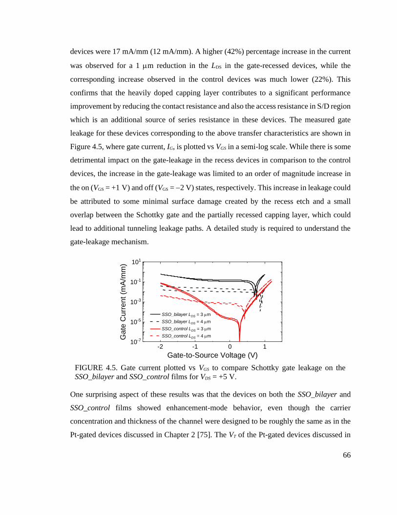
66
devices were 17 mA/mm (12 mA/mm). A higher (42%) percentage increase in the current
was observed for a 1 m reduction in the LDS in the gate-recessed devices, while the
corresponding increase observed in the control devices was much lower (22%). This
confirms that the heavily doped capping layer contributes to a significant performance
improvement by reducing the contact resistance and also the access resistance in S/D region
which is an additional source of series resistance in these devices. The measured gate
leakage for these devices corresponding to the above transfer characteristics are shown in
Figure 4.5, where gate current, IG, is plotted vs VGS in a semi-log scale. While there is some
detrimental impact on the gate-leakage in the recess devices in comparison to the control
devices, the increase in the gate-leakage was limited to an order of magnitude increase in
the on (VGS = +1 V) and off (VGS = −2 V) states, respectively. This increase in leakage could
be attributed to some minimal surface damage created by the recess etch and a small
overlap between the Schottky gate and the partially recessed capping layer, which could
lead to additional tunneling leakage paths. A detailed study is required to understand the
gate-leakage mechanism.
One surprising aspect of these results was that the devices on both the SSO_bilayer and
SSO_control films showed enhancement-mode behavior, even though the carrier
concentration and thickness of the channel were designed to be roughly the same as in the
Pt-gated devices discussed in Chapter 2 [75]. The VT of the Pt-gated devices discussed in
-2 -1 0 110-7
10-5
10-3
10-1
101
Ga
te C
urr
en
t (m
A/m
m)
Gate-to-Source Voltage (V)
SSO_bilayer LDS = 3 m
SSO_bilayer LDS = 4 m
SSO_control LDS = 3 m
SSO_control LDS = 4 m
FIGURE 4.5. Gate current plotted vs VGS to compare Schottky gate leakage on the
SSO_bilayer and SSO_control films for VDS = +5 V.

67
Chapter 2 was roughly -2 V. The VT is extracted for the recessed and control devices, with
LG = 3 m, fabricated here using the same method as in Chapter 2 (Equation 2.2) and found
to be 0.25 V and 0.5 V, respectively. This drastic change in VT may be attributed to surface
states in the SSO_bilayer and SSO_control films that could be additionally depleting the
channel apart from the Schottky gates. It is suspected that the O2 plasma clean or the Al2O3
wet etch could be the source of these depleting surface states. It must be noted that the Pt-
devices in Chapter 2 were annealed after the gate was deposited as a result of which a one-
to-one comparison must be considered with caution. Irrespective of the change in VT, the
value of the peak gm in the recessed device with Ni-gate on the SSO_bilayer film with LDS
= 3 m was found to be 65 mS/mm which is a ~4× improvement over the Pt-devices
discussed in Chapter 2, while the corresponding control device showed a ~2×
improvement. The larger improvement observed in recess devices over our prior Pt-devices
is due to the additional reduction in S/D access region, owing to the heavily doped capping
layer. The control devices also register a significant improvement because of the large
reduction in contact resistance by using Ti-contacts, as described in Chapter 3. These
results validate the effectiveness of the recess device structure.
The output characteristics, where ID is plotted vs VDS are shown Figure 4.6(a) and (b) for
recess and control devices with LDS = 3 m. ID is plotted for several values of VGS from
−2 V to +1 V. Both devices demonstrate typical n-FET behavior but with an unexpectedly
FIGURE 4.6. Output characteristics of MESFETs on (a) SSO_bilayer and (b)
SSO_control films. LG = 0.5 m, LDS = 3 m. Values of VGS were varied from +1.0 V to
−0.5 V in steps of −0.1 V.

68
large output conductance. The reason for the larger-than-expected output conductance is
not clear, but could be related to surface defects.
4.2.2 Pt Schottky Devices
Pt-gated devices were fabricated only on SSO_bilayer films and are discussed in this sub-
section. These devices exhibited a tendency to drift under certain conditions which caused
its VT to shift gradually. During the course of the entire measurements the devices
transitioned from being enhancement-mode to depletion-mode devices. The devices were
eventually stabilized after thermal annealing. The transient device behavior and post-
annealing measurements are discussed in the following two sub-sections.
4.2.2.1 Transient Device Behavior
Initial transfer characteristics of the Pt-devices are shown in Figure 4.7(a), where ID vs VGS
curves are shown for a device with LG = 1 m, and LDS = 9 m. Two successive
measurements obtained on this device are shown in Figure 4.7(a), where a clear shift in the
VT of the device can be seen with the shift being in the decreasing or negative direction,
leading to a significant increase in ID. The corresponding two output characteristics (ID vs
VDS) obtained for this device are shown in Figure 4.7(b). Upon application of a slightly
higher VDS voltage (10 V), the device VT shifted to even more negative values. As the VT
shifted further to more negative values, the ID also increased for a given VGS > VT. Noting
FIGURE 4.7. (a) Transfer and (b) output characteristics of a MESFET showing the
change in threshold voltage of the device observed in two subsequent measurements.
LG = 1 m, and LDS = 9 m.

69
this instability in the device, along with the larger-than-expected output conductance
similar to that observed in Ni-gated devices, thermal annealing at a relatively-low
temperature of 200 was attempted to help the stabilize the device. The device behavior
post-thermal annealing is discussed in the next sub-section.
4.2.2.2 Anomalous Device Behavior after Thermal Annealing
The device characteristics dramatically changed after a 200 annealing to a depletion-
mode behavior along with a large increase in the drive current in the device. However, the
device initially showed some hysteresis while the transfer characteristics were being
measured. As shown in Figure 4.8(a), the VT of the device can be clearly observed to be
negative. The hysteresis indicated that the device might still be unstable. In an attempt to
remove the hysteresis and stabilize the device, successive measurements were performed
on the device. While the device continued to drift initially, it eventually stabilized with a
VT = -5 V. The transfer characteristics obtained after stabilizing the device, along with the
initial measurement obtained after annealing, and an intermediate measurement are shown
in Figure 4.8(a). Further measurements attempted on this device did not show any
appreciable change in VT. The gm is plotted in Figure 4.8(b) corresponding to the transfer
characteristics obtained after the device was stabilized.
FIGURE 4.8. (a) Transfer characteristics of a recessed Pt-gated MESFET on the
SSO_bilayer film measured after thermal annealing at 200 . The device was initially
showed large hysteresis. After stabilization the hysteresis is reduced and VT changed to
−5 V. LG = 1 m, and LDS = 9 m. (b) Transconductance of the MESFET after VT
stabilization.

70
The output characteristics obtained for this device after the VT was stabilized are shown in
Figure 4.9(a). The output characteristics clearly show that a finite output conductance is
still present in the device. While the instabilities in the device and the changes after
annealing are not clearly understood, the device is now closer to the expected depletion-
mode behavior that was originally intended and confirmed by simulations presented in
Chapter 2. This indicates that the surface depletion may have been reversed partially by the
annealing. A thorough dedicated study is needed to understand the dependence of surface
depletion on temperature. The gate current corresponding to all the measurements
discussed above are plotted in Figure 4.9(b) to show the effect of VT shift and thermal
annealing on the leakage. Clearly, the VT shift and the annealing do not have a desirable
effect on the gate leakage. Methods to eliminate or reduce surface depletion without
impacting the gate leakage negatively need to be devised. Moving to a heterostructure or
metal-insulator-FET configuration can eliminate the additional surface depletion created
during the fabrication by avoiding exposure of SSO surface to any plasma or etching.
In some devices on SSO_control films, Ni-gates were redeposited, where the Pt-gate
fabrication failed due to a poor liftoff yield. The substrate was annealed at 200 before
the Ni-gates were redeposited. Such devices also showed anomalous high-currents that was
not observed in other Ni-gated devices. It is suspected that a small amount of Pt-residue
FIGURE 4.9. (a) Output characteristics of a Pt-gated MESFET after VT was stabilized
at −5 V. LG = 1 m, and LDS = 9 m. (b) Drain current and gate current vs VGS
corresponding to several measurements of the same device plotted on semi-log scale to
show the effect of annealing on gate leakage.

71
may have remained on the SSO surface after the liftoff failure, which when subjected to
annealing changed the effective carrier concentration in the underlying SSO, thus causing
this anomalous device behavior. Transfer characteristics and gate-leakage currents of two
such Ni-gated devices are shown in Figure 4.10. A clear depletion-mode behavior and
unusually high gate-leakage occur, which were not observed in other Ni-gated devices.
In conclusion, recess-gated MESFETs were fabricated for the first-time on SSO and a 2×
improvement in device performance is shown over control devices on single-layer epi
structures. Devices without annealing showed enhancement-mode behavior which is not
expected based on simulations. After annealing the devices, a large shift in the 𝑉𝑇 of the
devices is observed. This shift is not clearly understood but indicates that standard
fabrication processes may be causing a surface depletion that changes the effective carrier
concentration in the SSO films. This may be addressed by avoiding the exposure of SSO
to plasma or other etches. The currents in excess of 100 mA/mm on SSO-FETs with LDS
spacing as large as 9 m promises significant potential for SSO, and stannates in general
to produce high-performance FETs in the future.
4.3 RF Measurement Results
Initial RF measurements were performed on the MESFET devices fabricated on
SSO_control films. These measurements were performed using a Keysight E5063A RF
FIGURE 4.10. (a) Transfer characteristics of two Ni-gated devices on SSO_control
films where Pt had delaminated after a failed lift-off. (b) Gate current vs VGS for the
same two devices.

72
network analyzer in air at room temperature. Preliminary results indicate that SSO
MESFETs can have high operating frequencies. Figure 4.11(a) and (b) show the plots of
current gain, h21, and Mason’s unilateral gain, U, (in dB) vs. measurement frequency for a
MESFET with LG = 0.5 m, and LDS = 4 m. The MESFETs fabricated on the SSO_control
film, as can be seen from Figure 4.11, has an fT = 400 MHz, and an fmax = 1.2 GHz. Here,
the gain vs frequency curves are plotted for various values of VGS from 0 V to 1.1 V, for a
VDS = 5 V. In order explain the cut-off frequency, values obtained from DC characteristics
were also measured. The corresponding DC transfer characteristics and transconductance
of this MESFET are plotted in Figure 4.12(a) and (b), respectively. In 4.12(a) and (b), two
sets of curves are shown which were measured on this MESFET before (black) and after
(red) performing the RF measurements. The transfer characteristic obtained after the RF
measurement has a very high off current accompanied by substantial reduction in gm, in
comparison to the initial measurement characteristics. The increase in the Schottky gate
leakage can be modeled as a shunt resistance in the small-signal equivalent circuit and
explain the measured fmax being greater than the fT. The high fmax despite the leaky gate and
low gm indicates that the device RF performance could have been much better if not for the
aberrant shorting of the gate. Further improvements in RF performance should be possible
if improved device stability can be achieved.
FIGURE 4.11. Extracted gains (a) h21, (b) U are plotted vs measurement frequency. A
dashed orange line with a slope of -20 dB/dec is also added for convenience to compare
the roll-off characteristics of the device. fmax = 1.2 GHz and fT = 0.4 GHz is observed
for a device with LG = 0.5 m, and LDS = 4 m.

73
FIGURE 4.12. (a) Drain current, and (b) transconductance plotted vs. gate voltage. Two
sets of curves measured are shown: before (black) and after (red) a gate degradation that
likely occurred while the RF measurements were being obtained.

74
Chapter 5
Outlook and Conclusions

75
6.1 Conclusions
The vast potential offered by the perovskite oxide material system was reviewed in Chapter
1 and the realization of novel devices based on this material system may hinge on
identification of an apt perovskite oxide semiconductor. Perovskite stannates possess
several necessary material properties that are required of a semiconductor to be useful as a
channel material. Among the stannates, SSO, due to its wider band gap and smaller lattice
constant than that of BSO may be better suited to high-power and RF device applications
and also in general to other novel heterostructure devices.
In Chapter 2, single-layer SSO MESFET results were presented, which despite being the
first-ever SSO-based device results, were shown to have superior performance than any
prior perovskite oxide-based FETs. The electron affinity of SSO was confirmed using the
experimentally determined Pt-SSO Schottky barrier height. The key processing difficulties
identified here paved the way for the following experimental studies. In Chapter 3, key
issues revealed in the preliminary SSO MESFET devices, namely a high-contact resistance
and contact degradation in air were addressed. A first systematic study of Ohmic contacts
to any stannates was presented. Improved contact resistances with specific resistivity of Ti-
SSO contacts as low as 34 −cm2 were produced. These results can significantly benefit
future SSO-based RF devices. Additionally, the advantage of a bi-layer film structure in
terms of contact resistance improvement was proven. These results could be improved
further in future by utilizing a heavily doped BSO-capping layer which can potentially
reduce the contact resistance as BSO is capable of higher doping concentrations than in
SSO.
In Chapter 4, SSO bi-layer MESFETs in a recess-gate configuration were demonstrated
and improvement in device performance due to the use of the recess structure was shown.
A recess etch was demonstrated to aid in successful fabrication of such structures, which
can be extended in future to other perovskite stannate materials and even heterostructures
based on SSO. Peculiar device behavior was observed in Pt-gated devices before and after
annealing which helped identify surface depletion as a major obstacle to fabrication of

76
SSO-based MESFETs with superior DC performance. Alternate device structures to
mitigate this issue may be explored in future.
The work performed as a part of this dissertation is a first such study on SSO and is a
stepping-stone towards the development of future novel perovskite-based devices. SSO has
unique advantages over other emerging ultra-wide gap (UWG) semiconductors, including
-Ga2O3, diamond, and AlN by virtue of being a perovskite oxide semiconductor with the
capability of heterostructure integration with multifunctional perovskite oxides. Moreover,
initial studies indicate that SSO (and BSO) can have higher intrinsic theoretical mobility
limits than -Ga2O3 [46], which is presently the most extensively studied emerging UWG
semiconductor. Despite its tremendous promise, many fundamental questions remain as to
how to design and implement RF transistors using SrSnO3 materials. This could be the
focus of future work on SSO-based devices.
6.2 Proposed Future Work
6.2.1 Achieving High-Power Operation
Despite the promise of higher breakdown voltages in SSO owed to its wide band gap of 4-
5 eV, the critical breakdown fields in SSO have not been experimentally determined so far.
To this end, the SSO MESFETs fabricated on thin films described in Chapter 2 were used
to understand breakdown properties of these devices. Low breakdown voltages of ~30 V
were observed in these devices for a 𝐿𝐺𝐷 spacing of 8 m. The breakdown was observed
to occur in the on state of the device which is unusual because the on state is usually not
associated with high-electric fields that can trigger impact ionization. The output
characteristics of the device corresponding to this breakdown event is shown in Figure
5.1(a). Measurement of another device, whose breakdown was observed near the off state,
is shown in Figure 5.1(b). This device also had similar breakdown voltages. Both the
breakdown events were catastrophic and subsequent measurements on these devices were
not possible.
One observation is that the MESFETs, which were designed to have a relatively high
doping in the channel are not considered to be suitable for breakdown measurements

77
because of a relatively-large gate leakage under large negative biases, due to tunneling.
Moreover, the devices were not field-plate passivated [71] which is commonly required,
especially in MESFETs, to reduce the electric field-line crowding near the drain-side edge
of the gate. In the absence of a field-plate in MESFETs with high channel doping even
relatively smaller reverse bias voltages can cause large leakage currents eventually leading
to breakdown or possibly device burnout. These reasons make the SSO MESFET designs
fabricated, so far, as a part of this dissertation work to be unsuitable for breakdown
measurements.
In the future, devices with a field-plate structure and preferably in a MOSFET geometry
may be attempted to study the ideal breakdown in these devices. For MOSFETs,
identifying a suitable dielectric as gate oxide is critical. While ALD dielectrics, such as
HfO2 and Al2O3, can be used, their dielectric constants can be lower than that of SSO,
which can be detrimental to high-power applications as the breakdown voltage may then
depend on the peak electric fields and critical breakdown fields of the ALD dielectrics. It
could be beneficial to make use of the vast material choices available in the perovskite
oxide family to identify a gate oxide material with a higher dielectric constant that can be
deposited in situ and epitaxially. The epitaxially grown gate oxide can provide a good
interface with SSO which is crucial for a MOSFET and for high-power operation as well.
A higher dielectric constant in the gate oxide will also allow for modulation of higher
FIGURE 5.1. (a) On state breakdown in a single-layer Pt-gated MESFET with Sc-
contacts. (b) Off state breakdown in another similar MESFET. LGD = 8 m in the both
devices.

78
charge densities in the channel which can then be exploited to achieve higher drive currents
as well as DC and RF performance improvements.
As stated above, films with low doping are preferred to measure the breakdown voltage of
a Schottky-gated device. With this in mind, a thin SSO film with a 11 nm NID buffer layer
was first grown, and a 11 nm moderately doped active layer was subsequently grown by
setting the La effusion cell at a temperature of 1080 . Surface depletion caused the film
to be insulating and prevented any Hall mobility and sheet resistance extraction. Based on
doping calibrations, the dopant concentration is expected to be in the range of 1018 cm-3 to
5 × 1018 cm-3. To measure the breakdown voltage in these films, interdigitated capacitance
structures (IDCs) were fabricated and an optical micrograph of one such structure is shown
in Figure 5.2. These structures consist of an anode and a cathode which are both Schottky-
type contacts, which ensures that the current flowing through the anode and cathode is very
low. The fabrication procedure consisted of only one step, as a result of which alignment
marks were not required. The separation between the two Schottky contacts determines the
breakdown field in these structures. Electron-beam lithography was used to pattern the
features and Pt (10 nm) and Au (40 nm) was deposited and lifted off.
IDC devices with inter-electrode spacings of 2 m were measured up to a voltage of 200 V
and no breakdown was observed in these devices suggesting a breakdown field of at least
1 MV/cm in SSO, which is an encouraging preliminary result. The current-voltage
characteristics obtained on these IDC structures are shown in Figure 5.3. The current-
voltage curves that are shown were extracted from the measured data after correcting for
FIGURE 5.2. Optical micrograph of an IDC structure with 2 m spacing between the
Schottky contact fingers. Width of the device = 50 m.

79
the displacement current. While a slight increase in current for higher applied voltage was
observed, this current can be attributed to a slight leakage through the Schottky electrodes
as well as a residual displacement current remaining due to the use of an imperfect method
to de-embed the displacement current from measurement data. Due to lack of a high-
voltage supply which can provide > 200 V bias, further measurements were not performed
on these devices. These preliminary results are encouraging and suggest potential high-
power applications for SSO. Similar structures can be studied on undoped SSO films to
determine the intrinsic breakdown fields.
6.2.1.1 Inverse Capped Structure
In order to make best use of the key advantage of the stannates, viz. the ability to achieve
high-mobilities at high doping levels and the wide gap of SSO, an inverse capped film
structure whose schematic is shown in Figure 5.4 is proposed. In this structure, the active
layer is capped with a near-intrinsically-doped SSO layer which can be then used to
FIGURE 5.4. Schematic of an inverse capped structure, where the insulating capping
layer can suppress gate leakage and may help in measuring higher breakdown voltages.
-200 -100 0 100 200100a
1f
10f
100f
1p
10p
100p
1n
Curr
ent (A
)
Voltage (V)
FIGURE 5.3. Current vs voltage curves for a 2 m spacing IDC device showing no
breakdown occurring when measured up to 200 V. Width of the device = 50 m.

80
fabricate MESFETs whose gate leakage will be vastly minimized because of the low (or
no) doping in the capping layer. This structure can be useful to study breakdown
performance of SSO while retaining the higher doping in the channel which can help
achieve high currents, transconductance, and good RF performance. The capping layer may
possibly address some of the surface depletion effects observed in current SSO thin films,
although this is yet to be verified experimentally.
6.2.2 Path Forward to Heterostructures
The proposed inverse capped structure can also act as a natural transition step to move
towards heterostructures, which can be achieved by doping the capping layer with other
atoms that can increase the band offset with respect to the active layer and potentially the
dielectric constant in the capping layer. Heterostructures have helped achieve superior
performance in the devices based on III-V material system owing to the superior mobilities
that electrons can possess in a two-dimensionally confined state. Also, the advantage of
multifunctionality in perovskite oxide material world simply cannot be utilized if
heterostructures are not incorporated. The foundation laid down in this dissertation work,
provides the necessary framework for heterostructure device experiments and the results
of such experiments may well decide the fate of stannates as channel materials. It was
revealed in Chapter 1 that SSO is an ultra-wide band (UWG) semiconductor with band gap
in the range of 4-5 eV. Materials with a wide gap (WG) can have higher intrinsic
breakdown fields than their counterparts with narrow band gap. Existing WG
semiconductors, including GaN and SiC have been shown to have larger intrinsic
breakdown fields than narrow gap semiconductors, including Si and GaAs [89]. Emerging
UWG materials, including -Ga2O3, diamond, and AlN are being studied for future high-
power, extreme environment, and other novel applications, and can have breakdown fields
larger than those of WG semiconductors [89]. SSO has the potential to be added to the
emerging UWG materials list owing to its band gap > 4 eV. However, many of the
fundamental material properties, including thermal conductivity and intrinsic breakdown
field of SSO are as yet unknown and further work is required to uncover the potential for
SSO in high-power applications.

81
Bibliography
[1] J. Mannhart and D. G. Schlom, “Oxide interfaces—an opportunity for
electronics,” Science, vol. 327, no. 5973, pp. 1607–1611, 2010.
[2] M. Bibes, J. E. Villegas, and A. Barthélémy, “Ultrathin oxide films and interfaces
for electronics and spintronics,” Adv. Phys., vol. 60, no. 1, pp. 5–84, 2011.
[3] T. Wu, W. Pisula, M. Y. A. Rashid, and P. Gao, “Application of perovskite‐
structured materials in field‐effect transistors,” Adv. Electron. Mater., vol. 5, no. 12,
1900444, 2019.
[4] K. Ueno, S. Nakamura, H. Shimotani, A. Ohtomo, N. Kimura, T. Nojima, H. Aoki,
Y. Iwasa, and M. Kawasaki, “Electric-field-induced superconductivity in an
insulator,” Nat. Mater., vol. 7, no. 11, pp. 855–858, 2008.
[5] K. S. Takahashi, M. Gabay, D. Jaccard, K. Shibuya, T. Ohnishi, M. Lippmaa, and J.-
M. Triscone, “Local switching of two-dimensional superconductivity using the
ferroelectric field effect,” Nature, vol. 441, no. 7090, pp. 195–198, 2006.
[6] T. Kanki, H. Tanaka, and T. Kawai, “Electric control of room temperature
ferromagnetism in a Pb(Zr0.2Ti0.8)O3∕La0.85Ba0.15MnO3 field-effect transistor,” Appl.
Phys. Lett., vol. 89, no. 24, 242506, 2006.
[7] X. Li, P. Dang, J. Casamento, Z. Zhang, O. Afuye, A. B. Mei, A. B. Apsel, D. G.
Schlom, D. Jena, D. C. Ralph, and H. G. Xin, “Spin-orbit-torque field-effect

82
transistor (SOTFET): proposal for a new magnetoelectric memory,” arXiv preprint
arXiv:1909.08133, 2019.
[8] D. M. Newns, J. A. Misewich, C. C. Tsuei, A. Gupta, B. A. Scott, and A. Schrott,
“Mott transition field effect transistor,” Appl. Phys. Lett., vol. 73, no. 6, pp. 780–782,
1998.
[9] J. Son, S. Rajan, S. Stemmer, and S. J. Allen, “A heterojunction modulation-doped
Mott transistor,” J. Appl. Phys., vol. 110, no. 8, 084503, 2011.
[10] L. Bjaalie, A. Janotti, B. Himmetoglu, and C. G. Van de Walle, “Turning SrTiO3 into
a Mott insulator,” Phys. Rev. B, vol. 90, no. 19, 195117, 2014.
[11] S. Raghavan, J. Y. Zhang, O. F. Shoron, and S. Stemmer, “Probing the metal-
insulator transition in BaTiO3 by electrostatic doping,” Phys. Rev. Lett., vol. 117, no.
3, 037602, 2016.
[12] Y. M. Kim, T. Markurt, Y. Kim, M. Zupancic, J. Shin, M. Albrecht, and K. Char,
“Interface polarization model for a 2-dimensional electron gas at the BaSnO3/LaInO3
interface,” Sci. Rep., vol. 9, no. 1, pp. 1-9, 2019.
[13] M. Boucherit, O. F. Shoron, T. A. Cain, C. A. Jackson, S. Stemmer, and S. Rajan,
“Extreme charge density SrTiO3/GdTiO3 heterostructure field effect
transistors,” Appl. Phys. Lett., vol. 102, no. 24, 242909, 2013.
[14] M. Boucherit, O. Shoron, C. A. Jackson, T. A. Cain, M. L. C. Buffon, C. Polchinski,
S. Stemmer, and S. Rajan, “Modulation of over 1014 cm−2 electrons in
SrTiO3/GdTiO3 heterostructures,” Appl. Phys. Lett., vol. 104, no. 18, 182904, 2014.
[15] Y. Feng, X. Jiang, E. Ghafari, B. Kucukgok, C. Zhang, I. Ferguson, and N. Lu,
“Metal oxides for thermoelectric power generation and beyond,” Adv. Compos.
Hybrid Mater., vol. 1, no. 1, pp. 114–126, 2017.
[16] H. Y. Hwang, Y. Iwasa, M. Kawasaki, B. Keimer, N. Nagaosa, and Y. Tokura,
“Emergent phenomena at oxide interfaces,” Nat. Mater., vol. 11, no. 2, pp. 103–113,
2012.
83
[17] L. Bjaalie, B. Himmetoglu, L. Weston, A. Janotti, and C. G. V. D. Walle, “Oxide
interfaces for novel electronic applications,” New J. Phys., vol. 16, no. 2, 025005,
2014.
[18] S. Mathews, “Ferroelectric field effect transistor based on epitaxial perovskite
heterostructures,” Science, vol. 276, no. 5310, pp. 238–240, 1997.
[19] P.-H. Xiang, S. Asanuma, H. Yamada, I. H. Inoue, H. Sato, H. Akoh, A. Sawa, K.
Ueno, H. Yuan, H. Shimotani, M. Kawasaki, and Y. Iwasa, “Strain-mediated phase
control and electrolyte-gating of electron-doped manganites,” Adv. Mater., vol. 23,
no. 48, pp. 5822–5827, 2011.
[20] J. Lourembam, J. Wu, J. Ding, W. Lin, and T. Wu, “Electric field tuning of phase
separation in manganite thin films,” Phys. Rev. B, vol. 89, no. 1, 014425, 2014.
[21] K. Ueno, I. H. Inoue, T. Yamada, H. Akoh, Y. Tokura, and H. Takagi, “Field-effect
transistor based on KTaO3 perovskite,” Appl. Phys. Lett., vol. 84, no. 19, pp. 3726–
3728, 2004.
[22] H. Nakamura, H. Takagi, I. H. Inoue, Y. Takahashi, T. Hasegawa, and Y. Tokura,
“Low temperature metallic state induced by electrostatic carrier doping of
SrTiO3,” Appl. Phys. Lett., vol. 89, no. 13, 133504, 2006.
[23] B. Himmetoglu and A. Janotti, “Transport properties of KTaO3 from first-
principles,” J. Phys.: Condens. Matter, vol. 28, no. 6, 065502, 2016.
[24] I. A. Leonidov, E. I. Konstantinova, M. V. Patrakeev, A. V. Chukin, and V. L.
Kozhevnikov, “Electron transport and mobility analysis in La/Sr co-doped CaMnO3–
δ,” J. Solid State Electrochem., vol. 21, no. 7, pp. 2099–2108, 2017.
[25] E. Mikheev, B. Himmetoglu, A. P. Kajdos, P. Moetakef, T. A. Cain, C. G. V. D.
Walle, and S. Stemmer, “Limitations to the room temperature mobility of two- and
three-dimensional electron liquids in SrTiO3,” Appl. Phys. Lett., vol. 106, no. 6,
062102, 2015.

84
[26] A. Janotti, D. Steiauf, and C. G. V. D. Walle, “Strain effects on the electronic
structure of SrTiO3: toward high electron mobilities,” Phys. Rev. B, vol. 84, no. 20,
201304, 2011.
[27] H. J. Kim, U. Kim, H. M. Kim, T. H. Kim, H. S. Mun, B.-G. Jeon, K. T. Hong, W.-
J. Lee, C. Ju, K. H. Kim, and K. Char, “High mobility in a stable transparent
perovskite oxide,” Appl. Phys. Express, vol. 5, no. 6, 061102, 2012.
[28] H. J. Kim, U. Kim, T. H. Kim, J. Kim, H. M. Kim, B.-G. Jeon, W.-J. Lee, H. S. Mun,
K. T. Hong, J. Yu, K. Char, and K. H. Kim, “Physical properties of transparent
perovskite oxides (Ba,La)SnO3 with high electrical mobility at room
temperature,” Phys. Rev. B, vol. 86, no. 16, 165205, 2012.
[29] H. F. Wang, Q. Z. Liu, F. Chen, G. Y. Gao, and W. Wu, “Transparent and conductive
oxide films with the perovskite structure: La- and Sb-doped BaSnO3,” J. Appl. Phys.,
vol. 101, 106105, 2007.
[30] Q. Liu, J. Dai, Z. Liu, X. Zhang, G. Zhu, and G. Ding, “Electrical and optical
properties of Sb-doped BaSnO3 epitaxial films grown by pulsed laser deposition,” J.
Phys. D: Appl. Phys., vol. 43, no. 45, 455401, 2010.
[31] W.-J. Lee, H. J. Kim, J. Kang, D. H. Jang, T. H. Kim, J. H. Lee, and K. H. Kim,
“Transparent perovskite barium stannate with high electron mobility and thermal
stability,” Annu. Rev. Mater. Res., vol. 47, no. 1, pp. 391–423, 2017.
[32] H.-R. Liu, J.-H. Yang, H. J. Xiang, X. G. Gong, and S.-H. Wei, “Origin of the
superior conductivity of perovskite Ba(Sr)SnO3,” Appl. Phys. Lett., vol. 102, no. 11,
112109, 2013.
[33] D. G. Schlom, “Perspective: oxide molecular-beam epitaxy rocks!,” APL Mater.,
vol. 3, no. 6, 062403, 2015.
[34] A. Prakash, J. Dewey, H. Yun, J. S. Jeong, K. A. Mkhoyan, and B. Jalan, “Hybrid
molecular beam epitaxy for the growth of stoichiometric BaSnO3,” J. Vac. Sci. &
Technol. A: Vacuum, Surfaces, and Films, vol. 33, no. 6, 060608, 2015.

85
[35] S. Raghavan, T. Schumann, H. Kim, J. Y. Zhang, T. A. Cain, and S. Stemmer, “High-
mobility BaSnO3 grown by oxide molecular beam epitaxy,” APL Mater., vol. 4, no.
1, 016106, 2016.
[36] A. Prakash, P. Xu, X. Wu, G. Haugstad, X. Wang, and B. Jalan, “Adsorption-
controlled growth and the influence of stoichiometry on electronic transport in hybrid
molecular beam epitaxy-grown BaSnO3 films,” J. Mater. Chem. C, vol. 5, no. 23,
pp. 5730–5736, 2017.
[37] H. Paik, Z. Chen, E. Lochocki, A. S. H., A. Verma, N. Tanen, J. Park, M. Uchida, S.
Shang, B.-C. Zhou, M. Brützam, R. Uecker, Z.-K. Liu, D. Jena, K. M. Shen, D. A.
Muller, and D. G. Schlom, “Adsorption-controlled growth of La-doped BaSnO3 by
molecular-beam epitaxy,” APL Mater., vol. 5, no. 11, 116107, 2017.
[38] T. Wang, L. R. Thoutam, A. Prakash, W. Nunn, G. Haugstad, and B. Jalan, “Defect-
driven localization crossovers in MBE-grown La-doped SrSnO3 films,” Phys. Rev.
Mater., vol. 1, no. 6, 061601, 2017.
[39] T. Truttmann, A. Prakash, J. Yue, T. E. Mates, and B. Jalan, “Dopant solubility and
charge compensation in La-doped SrSnO3 films,” Appl. Phys. Lett., vol. 115, no. 15,
152103, 2019.
[40] T. Schumann, S. Raghavan, K. Ahadi, H. Kim, and S. Stemmer, “Structure and
optical band gaps of (Ba,Sr)SnO3 films grown by molecular beam epitaxy,” J. Vac.
Sci. & Technol. A: Vacuum, Surfaces, and Films, vol. 34, no. 5, 050601, 2016.
[41] A. Prakash, P. Xu, A. Faghaninia, S. Shukla, J. W. Ager, C. S. Lo, and B. Jalan,
“Wide bandgap BaSnO3 films with room temperature conductivity exceeding 104 S
cm−1,” Nat. Commun., vol. 8, no. 1, pp. 1-9, 2017.
[42] S. A. Chambers, T. C. Kaspar, A. Prakash, G. Haugstad, and B. Jalan, “Band
alignment at epitaxial BaSnO3/SrTiO3(001) and BaSnO3/LaAlO3(001)
heterojunctions,” Appl. Phys. Lett., vol. 108, no. 15, 152104, 2016.
[43] W. Nunn, A. Prakash, A. Bhowmik, R. Haislmaier, J. Yue, J. M. G. Lastra, and B.
Jalan, “Frequency- and temperature-dependent dielectric response in hybrid

86
molecular beam epitaxy-grown BaSnO3 films,” APL Mater., vol. 6, no. 6, 066107,
2018.
[44] H. Yun, M. Topsakal, A. Prakash, K. Ganguly, C. Leighton, B. Jalan, R. M.
Wentzcovitch, K. A. Mkhoyana, and J. S. Jeong, “Electronic structure of BaSnO3
investigated by high-energy-resolution electron energy-loss spectroscopy and ab
initio calculations,” J. Vac. Sci. & Technol. A, vol. 36, no. 3, 031503, 2018.
[45] S. J. Allen, S. Raghavan, T. Schumann, K.-M. Law, and S. Stemmer, “Conduction
band edge effective mass of La-doped BaSnO3,” Appl. Phys. Lett., vol. 108, no. 25,
252107, 2016.
[46] C. A. Niedermeier, S. Rhode, K. Ide, H. Hiramatsu, H. Hosono, T. Kamiya, and M.
A. Moram, “Electron effective mass and mobility limits in degenerate perovskite
stannate BaSnO3,” Phys. Rev. B, vol. 95, no. 16, 161202, 2017.
[47] K. Ganguly, “Structure and transport in epitaxial BaSnO3: doping, mobility and the
insulator-metal transition,” Diss. submitted to Univ. Minnesota, Chapter 1, 2018.
[48] A. Vegas, M. Vallet-Regí, J. M. González-Calbet, and M. A. Alario-Franco, “The
ASnO3 (A=Ca,Sr) perovskites,” Acta Crystallogr., Sect. B: Struct. Sci., vol. 42, no.
2, pp. 167–172, 1986.
[49] M. Glerup, K. S. Knight, and F. W. Poulsen, “High temperature structural phase
transitions in SrSnO3 perovskite,” Mater. Res. Bull., vol. 40, no. 3, pp. 507–520,
2005.
[50] E. Baba, D. Kan, Y. Yamada, M. Haruta, H. Kurata, Y. Kanemitsu, Y. Shimakawa,
"Optical and transport properties of transparent conducting La-doped SrSnO3 thin
films ", J. Phys. D: Appl. Phys., vol. 48, no. 45, 455106, 2015.
[51] W. Zhang, J. Tang, and J. Ye, “Structural, photocatalytic, and photophysical
properties of perovskite MSnO3 (M = Ca, Sr, and Ba) photocatalysts,” J. Mater. Res.,
vol. 22, no. 7, pp. 1859-1871, 2007.

87
[52] M. Wei, A. V. Sanchela, B. Feng, Y. Ikuhara, H. J. Cho, and H. Ohta, “High electrical
conducting deep-ultraviolet-transparent oxide semiconductor La-doped SrSnO3
exceeding ∼3000 S cm−1,” Appl. Phys. Lett., vol. 116, no. 2, 022103, 2020.
[53] A. M. Glazer, “The classification of tilted octahedra in perovskites,” Acta
Crystallogr., Sect. B: Struct. Crystallogr. Cryst. Chem., vol. 28, no. 11, pp. 3384–
3392, 1972.
[54] T. Wang, A. Prakash, Y. Dong, T. Truttmann, A. Bucsek, R. James, D. D. Fong, J.-
W. Kim, P. J. Ryan, H. Zhou, T. Birol, and B. Jalan, “Engineering SrSnO3 phases
and electron mobility at room temperature using epitaxial strain,” ACS Appl. Mater.
& Inter., vol. 10, no. 50, pp. 43802–43808, 2018.
[55] K. P. Ong, X. Fan, A. Subedi, M. B. Sullivan, and D. J. Singh, “Transparent
conducting properties of SrSnO3 and ZnSnO3,” APL Mater., vol. 3, no. 6, 062505,
2015.
[56] H. Wang, X. Jiao, Q. Liu, X. Xuan, F. Chen, and W. Wu, “Transparent and
conductive oxide films of the perovskite LaxSr1−xSnO3(x⩽ 0.15): epitaxial growth
and application for transparent heterostructures,” J. Phys. D: Appl. Phys., vol. 43, no.
3, 035403, 2010.
[57] L. Weston, L. Bjaalie, K. Krishnaswamy, and C. G. V. D. Walle, “Origins of n-type
doping difficulties in perovskite stannates,” Phys. Rev. B, vol. 97, no. 5, 054112,
2018.
[58] A. Ohtomo and H. Y. Hwang, “Surface depletion in doped SrTiO3 thin films,” Appl.
Phys. Lett., vol. 84, no. 10, pp. 1716–1718, 2004.
[59] L. F. J. Piper, L. Colakerol, P. D. C. King, A. Schleife, J. Zúñiga-Pérez, P.-A. Glans,
T. Learmonth, A. Federov, T. D. Veal, F. Fuchs, V. Muñoz-Sanjosé, F. Bechstedt,
C. F. Mcconville, and K. E. Smith, “Observation of quantized subband states and
evidence for surface electron accumulation in CdO from angle-resolved
photoemission spectroscopy,” Phys. Rev. B, vol. 78, no. 16, 165127, 2008.

88
[60] M. W. Allen, C. H. Swartz, T. H. Myers, T. D. Veal, C. F. Mcconville, and S. M.
Durbin, “Bulk transport measurements in ZnO: The effect of surface electron
layers,” Phys. Rev. B, vol. 81, no. 7, 075211, 2010.
[61] A. A. Kumar, A. Kumar, J. K. Quamara, G. R. Dillip, S. W. Joo, and J. Kumar,
“Fe(iii) induced structural, optical, and dielectric behavior of cetyltrimethyl
ammonium bromide stabilized strontium stannate nanoparticles synthesized by a
facile wet chemistry route,” RSC Adv., vol. 5, no. 22, pp. 17202–17209, 2015.
[62] F. Pan, D. Olaya, J. C. Price, and C. T. Rogers, “Thin-film field-effect transistors
based on La-doped SrTiO3 heterostructures,” Appl. Phys. Lett., vol. 84, no. 9, pp.
1573–1575, 2004.
[63] Q. Liu, L. Dong, Y. Liu, R. Gordon, P. D. Ye, P. Fay, and A. Seabaugh, “Frequency
response of LaAlO3/SrTiO3 all-oxide field-effect transistors,” Solid-State Electron.,
vol. 76, pp. 1–4, 2012.
[64] M. Hosoda, Y. Hikita, H. Y. Hwang, and C. Bell, “Transistor operation and mobility
enhancement in top-gated LaAlO3/SrTiO3 heterostructures,” Appl. Phys. Lett., vol.
103, no. 10, 103507, 2013.
[65] C. Woltmann, T. Harada, H. Boschker, V. Srot, P. A. V. Aken, H. Klauk, and J.
Mannhart, “Field-effect transistors with submicrometer gate lengths fabricated from
LaAlO3−SrTiO3-based heterostructures,” Phys. Rev. Appl., vol. 4, no. 6, 064003,
2015.
[66] A. Verma, S. Raghavan, S. Stemmer, and D. Jena, “Au-gated SrTiO3 field-effect
transistors with large electron concentration and current modulation,” Appl. Phys.
Lett., vol. 105, no. 11, 113512, 2014.
[67] C. Park, U. Kim, C. J. Ju, J. S. Park, Y. M. Kim and K. Char, “High mobility field
effect transistor based on BaSnO3 with Al2O3 gate oxide,” Appl. Phys. Lett., vol. 105,
no. 20, 203503, 2014.

89
[68] U. Kim, C. Park, T. Ha, Y. M. Kim, N. Kim, C. Ju, et al., “All-perovskite transparent
high mobility field effect using epitaxial BaSnO3 and LaInO3,” APL Mater., vol. 3,
no. 3, 036101, 2015.
[69] Y. M. Kim, C. Park, U. Kim, C. Ju and K. Char, “High-mobility BaSnO3 thin-film
transistor with HfO2 gate insulator,” Appl. Phys. Exp., vol. 9, no. 1, 011201, 2015.
[70] J. Shin, Y. M. Kim, Y. Kim, C. Park and K. Char, “High mobility BaSnO3 films and
field effect transistors on non-perovskite MgO substrate,” Appl. Phys. Lett., vol. 109,
no. 26, 262102, 2016.
[71] S. Sze and K. K. Ng, “Physics of semiconductor devices,” Wiley, 3rd ed., 2006.
[72] T. Alammar, I. Hamm, V. Grasmik, M. Wark, and A.-V. Mudring, “Microwave-
assisted synthesis of perovskite SrSnO3 nanocrystals in ionic liquids for
photocatalytic applications,” Inorg. Chem., vol. 56, no. 12, pp. 6920–6932, 2017.
[73] “Sentaurus device user guide,” Synopsys, San Jose, CA, 2008.
[74] A. Deneuville, “Characterization of the interface states at a Ag/Si interface from
capacitance measurements,” J. Appl. Phys., vol. 45, no. 7, pp. 3079–3084, 1974.
[75] V. R. S. K. Chaganti, A. Prakash, J. Yue, B. Jalan, and S. J. Koester, “Demonstration
of a depletion-mode SrSnO3 n-channel MESFET,” IEEE Elect. Dev. Lett., vol. 39,
no. 9, pp. 1381–1384, 2018.
[76] J. C. Rode, H.-W. Chiang, P. Choudhary, V. Jain, B. J. Thibeault, W. J. Mitchell, M.
J. W. Rodwell, M. Urteaga, D. Loubychev, A. Snyder, Y. Wu, J. M. Fastenau, and
A. W. K. Liu, “Indium phosphide heterobipolar transistor technology beyond 1-THz
bandwidth,” IEEE Trans. Elect. Dev., vol. 62, no. 9, pp. 2779–2785, 2015.
[77] C. S. Chu, Y. Zhou, K. Chen, and K. Lau, “Q-factor characterization of RF GaN-
based metal-semiconductor-metal planar interdigitated varactor,” IEEE Elect. Dev.
Lett., vol. 26, no. 7, pp. 432–434, 2005.
[78] S. N. Mohammad, “Contact mechanisms and design principles for alloyed ohmic
contacts to n-GaN,” J. Appl. Phys., vol. 95, no. 12, pp. 7940–7953, 2004.

90
[79] S. Arulkumaran, G. I. Ng, K. Ranjan, C. M. M. Kumar, S. C. Foo, K. S. Ang, S.
Vicknesh, S. B. Dolmanan, T. Bhat, and S. Tripathy, “Record-low contact resistance
for InAlN/AlN/GaN high electron mobility transistors on Si with non-gold
metal,” Japanese J. Appl. Phys., vol. 54, no. 4S, 04DF12, 2015.
[80] Z. Zhang, S. O. Koswatta, S. W. Bedell, A. Baraskar, M. Guillorn, S. U. Engelmann,
Y. Zhu, J. Gonsalves, A. Pyzyna, M. Hopstaken, C. Witt, L. Yang, F. Liu, J.
Newbury, W. Song, C. Cabral, M. Lofaro, A. S. Ozcan, M. Raymond, C. Lavoie, J.
W. Sleight, K. P. Rodbell, and P. M. Solomon, “Ultra low contact resistivities for
CMOS beyond 10-nm node,” IEEE Elect. Dev. Lett., vol. 34, no. 6, pp. 723–725,
2013.
[81] M. Urteaga, Z. Griffith, M. Seo, J. Hacker, and M. J. W. Rodwell, “InP HBT
technologies for THz integrated circuits,” Proc. IEEE, vol. 105, no. 6, pp. 1051–
1067, 2017.
[82] SD. Sekiya, H. Nakamura, and T. Kimura, “Enhanced carrier injection in perovskite
field-effect transistors via low-barrier contacts,” Appl. Phys. Exp., vol. 4, no. 6,
064103, 2011.
[83] M. D. Groner, F. H. Fabreguette, J. W. Elam, and S. M. George, “Low-temperature
Al2O3 atomic layer deposition,” Chem. Mater., vol. 16, no. 4, pp. 639–645, 2004.
[84] “The photographic periodic table of the elements,” [Online], Available:
https://periodictable.com/index.html.
[85] A. Ping, D. Selvanathan, C. Youtsey, E. Piner, J. Redwing, and I. Adesida, “Gate
recessing of GaN MESFETs using photoelectrochemical wet etching,” Electron.
Lett., vol. 35, no. 24, 2140, 1999.
[86] S. J. Hong, P. Chapman, P. T. Krein, and K. K. Kim, “Selective-area growth and
fabrication of recessed-gate GaN MESFET using plasma-assisted molecular beam
epitaxy,” Physica Status Solidi (a), vol. 203, no. 7, pp. 1872–1875, 2006.

91
[87] C.-H. Chen, S. Keller, E. D. Haberer, L. Zhang, S. P. Denbaars, E. L. Hu, U. K.
Mishra, and Y. Wu, “Cl2 reactive ion etching for gate recessing of AlGaN/GaN field-
effect transistors,” J. Vac. Sci & Technol. B, vol. 17, no. 6, 2755, 1999.
[88] J. Moon, S. Wu, D. Wong, I. Milosavljevic, A. Conway, P. Hashimoto, M. Hu, M.
Antcliffe, and M. Micovic, “Gate-recessed AlGaN-GaN HEMTs for high-
performance millimeter-wave applications,” IEEE Elect. Dev. Lett., vol. 26, no. 6,
pp. 348–350, 2005.
[89] J. Y. Tsao, S. Chowdhury, M. A. Hollis, D. Jena, N. M. Johnson, K. A. Jones, R. J.
Kaplar, S. Rajan, C. G. V. D. Walle, E. Bellotti, C. L. Chua, R. Collazo, M. E.
Coltrin, J. A. Cooper, K. R. Evans, S. Graham, T. A. Grotjohn, E. R. Heller, M.
Higashiwaki, M. S. Islam, P. W. Juodawlkis, M. A. Khan, A. D. Koehler, J. H. Leach,
U. K. Mishra, R. J. Nemanich, R. C. N. Pilawa-Podgurski, J. B. Shealy, Z. Sitar, M.
J. Tadjer, A. F. Witulski, M. Wraback, and J. A. Simmons, “Ultrawide-bandgap
semiconductors: research opportunities and challenges,” Adv. Elect. Mater., vol. 4,
no. 1, 1600501, 2017.

92
Appendix A: Optical
Photolithography Process
Flow

93
Soak the sample in acetone overnight before starting any processing. Gentle sonication
can help partially clean up any solder residue present near the edges of the substrates.
I. Dynamic dispense photoresist spin and exposure
1. Clean the substrate with acetone and IPA and perform a 120 ºC dehydration bake.
2. Use the headway spinner and set the spin speed to 5000 rpm after placing the
substrate on the vacuum chuck. Then use a pipette to dispense one drop of
photoresist (AZ® 1512) close to the center of the substrate while it is spinning.
Start the timer simultaneously and allow the substrate to spin at the set speed for
45 s.
3. Transfer the substrate to a 100 ºC hot plate and bake for 1 min.
4. After alignment, expose with hard contact for 5.5 s.
5. If necessary, perform image reversal. Image reversal bake has to be followed by
an additional exposure under Oriel lamp for 8 min. It is good practice to perform a
first exposure for 4 min and then expose the remaining 4 min after rotating the
substrate by 90º.
6. The develop time using standard developer provided by MNC is 30 s without any
image reversal. If image reversal is used, then the develop time is 3.5 min.
II. Alignment marks
1. It is important to have good and reliable alignment marks.
2. Ti (10 nm) / Al (50 nm) may be evaporated and lifted off.
III. Mesa
1. After mesa patterning, prepare a 1 M HCl solution and place it on a hot plate set
to 60 ºC. Allow the solution to rest on the hot plate for 30 min.
2. Perform wet etch for 1.5 min in 1 M HCl. Etch times longer than ~1.5 min can
result in significant lateral etching.

94
3. Then use Ar plasma dry etch for 10 min. The name of the recipe to be used here is
“slow_200_70_24”.
4. After this perform an O2 plasma clean with 100 W power for 20 s.
5. Soak overnight in acetone for resist strip.
IV. Ohmic Contacts
1. After patterning, perform O2 plasma clean with 50 W power for 20 s.
2. Load the substrates into the evaporation chamber and pump down for 1 hr.
3. Deposit Sc (10 nm) / Au (80 nm) and liftoff in acetone overnight.
4. Sonicate, if needed, using gentle powers for 5-10 s. Increase the sonication time
only if needed.
V. Schottky Contacts
1. After patterning, perform O2 plasma clean with 50 W power for 20 s.
2. Evaporate Pt (10 nm) / Ti (10 nm) / Al (80 nm) / Ti (10 nm) after pumping down
for 1 hr.
3. Watch the Pt deposition carefully and pause the process if the chamber pressure
exceeds 9 × 10⁻⁶ Torr during deposition. The process may be continued after
pressure is stabilized. Better to pump down for longer time before starting Pt
deposition in the beginning to avoid this. Slow ramp up process must be used for
efficient Pt deposition.
4. After liftoff, anneal at 300 ºC in Ar/H2 atmosphere for 5 min to activate the
Ohmic contacts.

95
Appendix B: E-beam
Lithography Process Flow

96
Soak the sample in acetone overnight before starting any processing. Gentle sonication
can help partially clean up any solder residue present near the edges of the substrates.
I. General PMMA spin and sample preparation
1. Clean the substrate with acetone and IPA and perform a 120 ºC dehydration bake.
2. After spinning PMMA, bake for 15 min at 180 ºC. Longer bakes will not hurt.
3. Use the SEM sputterer to deposit a thin Au layer. The recommended sputter time
is 30 s and must be increased only if a good reflection is not observed under the
alignment stage.
4. Use regular rectangular clips to hold the sample. Use of Cu clips may help but has
the downside of losing patternable sample area. It may also lead to unintentional
scratches.
II. Alignment marks
1. Spin MMA EL9 at 3000 rpm for 45 s. Bake at 180 ºC for 8 min and allow the
sample to cool down for 2 min.
2. Spin PMMA C2 at 3000 rpm for 45 s. Bake at 150 ºC for 15 min and allow the
sample to cool down for 2 min.
3. Sputter Au for 30 s.
4. Use 15 nm beam step size, 15 nA current and a dose of 250 C/cm2.
5. Strip Au using wet etchant (KI-based) for 2 min or longer, if needed.
6. Develop for 50 s in 3:1 IPA:water and rinse with water.
7. Perform O2 plasma clean using 100 W for 20 s.
8. Evaporate Ti (10 nm) / Au (90 nm) and lift-off.
III. Mesa
1. Use photolithography process described in Appendix A for patterning.
2. Use Ar plasma dry etch for 17.5 min. The name of the recipe to be used here is
“slow_200_70_24”. Etch rate is ~3 nm/min.

97
3. Perform O2 plasma clean using 100 W for 20 s.
4. Soak in acetone overnight to strip PMMA.
IV. First recess etch
1. Use photolithography process described in Appendix A for patterning.
2. Use “N-SrTiO3-8mt Low POWER” recipe in a dry run to clean the Oxford etcher
chamber for 2 min.
3. Then use the same recipe to partially etch the capping layer for 1.75 min. Etch
rate is 3.8 ± 0.7 nm/min as determined from profilometer measurements.
4. Soak in acetone for resist removal.
V. Ohmic contacts for LDS ≥ 2 m
1. Use photolithography process described in Appendix A for patterning.
2. Perform O2 plasma clean using 50 W for 30 s and then in Ar plasma for 45 s.
3. Evaporate Ti (75 nm) / Au (100 nm) and liftoff overnight in acetone. Sonicate
gently for 5-10s and repeat, if necessary.
VI. Ohmic contacts for LDS ≥ 2 m
1. Spin PMMA C6 at 2500 rpm for 60 s using ramp speed of 500 rpm/s. Bake at 180
ºC for 15 min.
2. Sputter Au for 30 s.
3. Use 50 nm beam step size, 100 nA current and a dose of 560 C/cm2.
4. Strip Au using wet etchant (KI-based) for 2 min or longer, if needed.
5. Develop for 40 s in 3:1 IPA:water and rinse with water.
6. Perform O2 plasma clean using 50 W for 30 s and then in Ar plasma for 45 s.
7. Evaporate Ti (75 nm) / Au (100 nm) and lift-off.
8. Anneal at 300 ºC in Ar/H2 atmosphere for 5 min.
9. Deposit 10 nm ALD Al2O3 at 200 ºC.

98
VII. Al2O3 etch for pads
1. Use photolithography process described in Appendix A for patterning.
2. Perform O2 plasma clean using 50 W for 30 s.
3. Etch Al2O3 using “N-HfO2 Etch Lower pwr” recipe for 15 s.
4. Strip resist in acetone overnight.
VIII. Schottky Contacts
1. Spin PMMA C6 at 4000 rpm for 60 s. Bake at 180 ºC for 15 min.
2. Sputter Au for 30 s.
3. Use 20 nm beam step size, 8 nA current and a dose of 800 C/cm2.
4. Strip Au using wet etchant (KI-based) for 2 min or longer, if needed.
5. Develop for 1 min in 3:1 IPA:water and rinse with water.
6. Perform O2 plasma clean using 50 W for 30s.
7. Etch Al2O3 using MF® 319 solution for 12 min.
8. Evaporate Ni (65 nm) / Ti (10 nm) / Au (80 nm) and lift-off.