Embed Size (px)
Citation preview

Strong terahertz absorption using SiO2/Al based metamaterial structuresFabio Alves, Brian Kearney, Dragoslav Grbovic, Nickolay V. Lavrik, and Gamani Karunasiri
Citation: Applied Physics Letters 100, 111104 (2012); doi: 10.1063/1.3693407 View online: http://dx.doi.org/10.1063/1.3693407 View Table of Contents: http://scitation.aip.org/content/aip/journal/apl/100/11?ver=pdfcov Published by the AIP Publishing Articles you may be interested in Characterization of SiO2/SiNx gate insulators for graphene based nanoelectromechanical systems Appl. Phys. Lett. 105, 123114 (2014); 10.1063/1.4896515 Study of spontaneous and induced absorption in amorphous Ta2O5 and SiO2 dielectric thin films J. Appl. Phys. 113, 133104 (2013); 10.1063/1.4799415 Strongly birefringent metamaterials as negative index terahertz wave plates Appl. Phys. Lett. 95, 171104 (2009); 10.1063/1.3253414 XRay Diffraction Studies of the Structures of Dynamically Compressed Be, Al, LiF, KCI, and SiO2 AIP Conf. Proc. 845, 1253 (2006); 10.1063/1.2263552 Origin of the stress-induced leakage currents in Al – Ta 2 O 5 SiO 2 – Si structures Appl. Phys. Lett. 86, 152104 (2005); 10.1063/1.1900955
This article is copyrighted as indicated in the article. Reuse of AIP content is subject to the terms at: http://scitation.aip.org/termsconditions. Downloaded to IP:
128.255.6.125 On: Sun, 28 Sep 2014 09:51:50
Strong terahertz absorption using SiO2/Al based metamaterial structures
Fabio Alves,1,a) Brian Kearney,1 Dragoslav Grbovic,1 Nickolay V. Lavrik,2
and Gamani Karunasiri11Department of Physics, Naval Postgraduate School, Monterey, California 93943, USA2Center for Nanophase Materials Sciences, Oak Ridge National Laboratory, Oak Ridge,Tennessee 37831, USA
(Received 26 September 2011; accepted 23 February 2012; published online 12 March 2012)
Metamaterial absorbers with nearly 100% absorption in the terahertz (THz) spectral band have
been designed and fabricated using a periodic array of aluminum (Al) squares and an Al ground
plane separated by a thin silicon dioxide (SiO2) dielectric film. The entire structure is less than
1.6 mm thick making it suitable for the fabrication of microbolometers or bi-material sensors for
THz imaging. Films with different dielectric layer thicknesses exhibited resonant absorption at 4.1,
4.2, and 4.5 THz with strengths of 98%, 95%, and 88%, respectively. The measured absorption
spectra are in good agreement with simulations using finite element modeling. VC 2012 AmericanInstitute of Physics. [http://dx.doi.org/10.1063/1.3693407]
Terahertz (THz) imaging has gained increased attention
because of its many distinctive properties, which makes it
attractive for security and medical applications.1 Despite the
availability of some terahertz sources and detectors, highly
sensitive THz imaging systems are still restricted to the
research domain. THz imaging has been demonstrated using
conventional, microbolometer-based imagers optimized for
infrared (IR) wavelengths (8-12 lm) paired with an external
THz illumination source.2,3 Potential limitations of this
approach are the low sensitivity in the THz region of micro-
bolometer cameras optimized for IR imaging and the rela-
tively low output power of commonly available THz sources
such as quantum cascade lasers (QCLs). Bi-material based
uncooled infrared imaging technology4,5 is another possible
candidate for THz imaging using the same principle as
microbolometers, but it suffers the same limitations in
performance.6 In both cases, the absorbed energy heats the
sensing element, changing its resistance in case of microbol-
ometers and deforming its structure in case of bimaterial sen-
sors. To increase the sensitivity of these devices, it is
necessary to modify the pixel membrane structure with
layers with high THz absorption, without compromising the
thermal proprieties of the sensors.6 Thus, relatively thin (less
than 2 lm) THz absorbing membranes are required, ideally
with absorption tuned to the QCL illuminator frequency.
One approach is to replace the pixel membrane with a meta-
material structure, tuned to the QCL frequency, to achieve
resonant absorption and, thus, high sensitivity. One con-
straint is that the materials used should have structural and
thermal properties compatible with fabrication of microelec-
tromechanical system (MEMS) based bi-material sensor pix-
els.5 Several groups have reported the fabrication and
analysis of metamaterial structures operating in THz spectral
band using a variety of configurations including resonant ele-
ments and periodic arrays of metallic squares and rings.1,7–11
The common theme was to place a capacitive mesh close to
a conducting plane with a dielectric spacer in between to
form an artificial structure that exhibits electromagnetic
properties such that its impedance matches with the sur-
rounding media (free space in our case) at a specific fre-
quency.12 In this situation, ideally, there is no transmission
and no reflection resulting in total absorption. By controlling
shape, thickness, and properties of metallic and dielectric
layers, it is possible to tune the frequency and absorption am-
plitude of the resonance. This concept was employed to tune
absorption characteristics of microbolometers working in the
IR range.13 High absorption in THz range and even multi-
band capabilities have been achieved with thicker polyimide
and SiO2 dielectric layers.8,14
In this letter, we report the design and fabrication of
highly absorbent, thin metamaterial structures (less than
1.6 lm thick), using SiO2 and Al. The favorable combination
of thermal, mechanical, and optical properties of SiO2 and Al6
make them highly suitable to build membrane structures with
high absorption as well as large bi-material deflection. The
metamaterial structures are comprised of an array of Al
squares separated from an Al ground plane by a SiO2 layer as
schematically illustrated in Fig. 1(a). Each Al layer is about
100 nm thick, and the thickness of the SiO2 layer is varied
from 1 to 1.4lm. The entire structure was grown on a high re-
sistivity Si wafer for testing purposes. They were designed to
absorb frequencies in the 4–4.5 THz spectral region to take
advantage of the availability of high power QCLs in this fre-
quency range.3 The absorption characteristics of the structures
were simulated with 3D finite element modeling using COM-
SOL multiphysics software. Due to the periodicity of the
metamaterial structures, a unit cell as schematically shown in
Fig. 1(a) was used in the simulation. The field distribution is
calculated for a normally incident plane wave polarized along
one of the edges of the square and perfect electric and perfect
magnetic boundary conditions. The reflection spectrum of
1 W incident power is calculated by integrating the power
flow on the layer boundary, while transmission is considered
to be zero since the ground plane thickness is greater than the
skin depth of aluminum in this range of frequencies (80 nm
for aluminum at 4 THz). The index of refraction of SiO2 at
THz frequencies was taken from15,16 as 2.0þ 0.025i and con-
ductivity of 1� 107 S/m was used for Al.a)Electronic mail: [email protected].
0003-6951/2012/100(11)/111104/3/$30.00 VC 2012 American Institute of Physics100, 111104-1
APPLIED PHYSICS LETTERS 100, 111104 (2012)
This article is copyrighted as indicated in the article. Reuse of AIP content is subject to the terms at: http://scitation.aip.org/termsconditions. Downloaded to IP:
128.255.6.125 On: Sun, 28 Sep 2014 09:51:50
Three samples were fabricated using standard microfab-
rication techniques. Al ground planes, 95 nm thick, were de-
posited using e-beam evaporation. Dielectric SiO2 films of
1430 nm, 1235 nm, and 1035 nm thick were deposited using
plasma enhanced chemical vapor deposition (PECVD) for
samples A, B, and C, respectively. The dielectric film depo-
sition was followed by e-beam deposition of another layer of
Al film, 95 nm thick. Finally, square arrays were patterned,
using wet etching, on the top Al layer with sides 16.3 lm,
16.5 lm, and 15.3 lm for samples A, B, and C, respectively.
The periodicity of the squares is 21 lm for all of the samples.
Actual dimensions of the squares and periodicity of the sam-
ples were measured using optical microscopy. Note that the
variation of the squares dimensions was obtained by varying
the time in the etchant. The thicknesses of the layers were
measured using conventional stylus profilometry.
The three samples were characterized using a Fourier
transform infrared spectrometer (FTIR) extended to THz
range. The reflectance spectra were measured with FTIR
beam incident at 30� from the normal of the absorber arrays.
The details of the measurement can be found in Ref. 17. Fig-
ure 2 shows the measured reflection spectra of the three
samples.
Reflection minima of 2%, 5%, and 12% were found at
the frequencies of 4.1, 4.2, and 4.5 THz for samples A, B,
and C, respectively. The absorption spectrum of each sample
was obtained by evaluating (100 – T – R), where T is the
transmission coefficient (zero in this case) and R is the
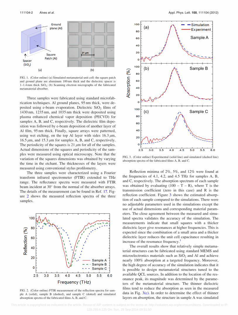
reflection coefficient. Figure 3 shows the estimated absorp-
tion of each sample compared to the simulations. There were
no adjustable parameters used in the simulations except the
use of actual dimensions and corresponding material param-
eters. The close agreement between the measured and simu-
lated spectra validates the accuracy of the simulation. The
measurements indicate that small squares with a thicker
dielectric layer give resonances at higher frequencies. This is
expected since the combination of a small area and a thicker
dielectric layer reduces the unit cell capacitance resulting in
increase of the resonance frequency.1
The overall results show that relatively simple metama-
terial structures can be fabricated using standard MEMS and
microelectronics materials such as SiO2 and Al and achieve
nearly 100% absorption at a targeted frequency. Moreover,
the high degree of accuracy of the simulation indicates that it
is possible to design metamaterial structures tuned to the
available QCL sources. In addition to the location of the res-
onance peak, its magnitude was determined by the parame-
ters of the metamaterial structure. The thinner dielectric
films tend to reduce the absorption as seen in the measured
data in Fig. 3(c). In order to determine the effect of thinner
layers on absorption, the structure in sample A was simulated
FIG. 1. (Color online) (a) Simulated metamaterial unit cell: the square patch
and ground plane are aluminum 100 nm thick and the dielectric spacer is
1–1.4 mm thick SiO2; (b) Scanning electron micrographs of the fabricated
metamaterial absorber.
FIG. 2. (Color online) FTIR measurement of the reflection spectra for sam-
ple A (solid), sample B (dashed), and sample C (dotted) and simulated
absorption spectra of the fabricated films A, B, and C.
FIG. 3. (Color online) Experimental (solid line) and simulated (dashed line)
absorption spectra of the fabricated films A, B, and C.
111104-2 Alves et al. Appl. Phys. Lett. 100, 111104 (2012)
This article is copyrighted as indicated in the article. Reuse of AIP content is subject to the terms at: http://scitation.aip.org/termsconditions. Downloaded to IP:
128.255.6.125 On: Sun, 28 Sep 2014 09:51:50
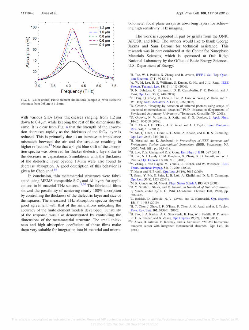
with various SiO2 layer thicknesses ranging from 1.2 lm
down to 0.4 lm while keeping the rest of the dimensions the
same. It is clear from Fig. 4 that the strength of the absorp-
tion decreases rapidly as the thickness of the SiO2 layer is
reduced. This is primarily due to an increase in impedance
mismatch between the air and the structure resulting in
higher reflection.13 Note that a slight blue shift of the absorp-
tion spectra was observed for thicker dielectric layers due to
the decrease in capacitance. Simulations with the thickness
of the dielectric layer beyond 1.4 lm were also found to
decrease absorption. A good description of this behavior is
given by Chen et al.18
In conclusion, thin metamaterial structures were fabri-
cated using MEMS compatible SiO2 and Al layers for appli-
cations in bi-material THz sensors.19,20 The fabricated films
showed the possibility of achieving nearly 100% absorption
by controlling the thickness of the dielectric layer and size of
the squares. The measured THz absorption spectra showed
good agreement with that of the simulations indicating the
accuracy of the finite element models developed. Tunability
of the response was also demonstrated by controlling the
dimensions of the metamaterial structure. The small thick-
ness and high absorption coefficient of these films make
them very suitable for integration into bi-material and micro-
bolometer focal plane arrays as absorbing layers for achiev-
ing high sensitivity THz imaging.
The work is supported in part by grants from the ONR,
AFOSR, and NRO. The authors would like to thank George
Jaksha and Sam Barone for technical assistance. This
research was in part conducted at the Center for Nanophase
Materials Sciences, which is sponsored at Oak Ridge
National Laboratory by the Office of Basic Energy Sciences,
U.S. Department of Energy.
1H. Tao, W. J. Padilla, X. Zhang, and R. Averitt, IEEE J. Sel. Top. Quan-
tum Electron. 17(1), 92 (2011).2A. W. M. Lee, B. S. Williams, S. Kumar, Q. Hu, and J. L. Reno, IEEE
Photon. Technol. Lett. 18(13), 1415 (2006).3B. N. Behnken, G. Karunasiri, D. R. Chamberlin, P. R. Robrish, and J.
Faist, Opt. Lett. 33(5), 440 (2008).4F. Dong, Q. Zhang, D. Chen, L. Pan, Z. Guo, W. Wang, Z. Duan, and X.
W. Dong, Sens. Actuators, A 133(1), 236 (2007).5D. Grbovic, “Imaging by detection of infrared photons using arrays of
uncooled micromechanical detectors,” Ph.D. dissertation (Department of
Physics and Astronomy, University of Tennessee, Knoxville, TN, 2008).6D. Grbovic, N. V. Lavrik, S. Rajic, and P. G. Datskos, J. Appl. Phys.
104(5), 054508 (2008).7H. T. Chen, J. F. O’Hara, A. K. Azad, and A. J. Taylor, Laser Photonics
Rev. 5(4), 513 (2011).8Y. Ma, Q. Chen, J. Grant, S. C. Saha, A. Khalid, and D. R. S. Cumming,
Opt. Lett. 36(6), 945 (2011).9H. Mosallaei and K. Sarabandi, in Proceedings of IEEE Antennas andPropagation Society International Symposium (IEEE, Piscataway, NJ,
2005), Vol. 1(B), pp. 615–618.10H. Luo, Y. Z. Cheng, and R. Z. Gong, Eur. Phys. J. B 81, 387 (2011).11H. Tao, N. I. Landy, C. M. Bingham, X. Zhang, R. D. Averitt, and W. J.
Padilla, Opt. Express 16(10), 7181 (2008).12Y. Zhang, J. von Hagen, M. Younis, C. Fischer, and W. Wiesbeck, IEEE
Trans. Antennas Propag. 51(10), 2704 (2003).13T. Maier and H. Bruckl, Opt. Lett. 34(19), 3012 (2009).14J. Grant, Y. Ma, S. Saha, L. B. Lok, A. Khalid, and D. R. S. Cumming,
Opt. Lett. 36(8), 1524 (2011).15M. K. Gunde and M. Macek, Phys. Status Solidi A 183, 439 (2001).16D. Y. Smith, E. Shiles, and M. Inokuti, in Handbook of Optical Constants
of Solids, edited by E. D. Palik (Academic, Chestnut Hill, 1998), pp.
306–406.17C. Bolakis, D. Grbovic, N. V. Lavrik, and G. Karunasiri, Opt. Express
18(14), 14488 (2010).18H. T. Chen, J. Zhou, J. F. O’Hara, F. Chen, A. K. Azad, and A. J. Taylor,
Phys. Rev. Lett. 105, 073901 (2010).19H. Tao, E. A. Kadlec, A. C. Strikwerda, K. Fan, W. J. Padilla, R. D. Aver-
itt, E. A. Shaner, and X. Zhang, Opt. Express 19(22), 21620 (2011).20F. Alves, D. Grbovic, B. Kearney, and G. Karunasiri, “MEMS bi-material
terahertz sensor with integrated metamaterial absorber,” Opt. Lett. (in
press).
FIG. 4. (Color online) Finite element simulations (sample A) with dielectric
thickness from 0.6 lm to 1.2 mm.
111104-3 Alves et al. Appl. Phys. Lett. 100, 111104 (2012)
This article is copyrighted as indicated in the article. Reuse of AIP content is subject to the terms at: http://scitation.aip.org/termsconditions. Downloaded to IP:
128.255.6.125 On: Sun, 28 Sep 2014 09:51:50