Embed Size (px)
Citation preview
ARTICLE
Received 11 Mar 2016 | Accepted 9 Nov 2016 | Published 21 Dec 2016
Strong confinement-induced engineering of theg factor and lifetime of conduction electron spinsin Ge quantum wellsAnna Giorgioni1, Stefano Paleari2, Stefano Cecchi3,w, Elisa Vitiello1, Emanuele Grilli1, Giovanni Isella3,
Wolfgang Jantsch4, Marco Fanciulli2 & Fabio Pezzoli1
Control of electron spin coherence via external fields is fundamental in spintronics. Its
implementation demands a host material that accommodates the desirable but contrasting
requirements of spin robustness against relaxation mechanisms and sizeable coupling
between spin and orbital motion of the carriers. Here, we focus on Ge, which is a prominent
candidate for shuttling spin quantum bits into the mainstream Si electronics. So far, however,
the intrinsic spin-dependent phenomena of free electrons in conventional Ge/Si
heterojunctions have proved to be elusive because of epitaxy constraints and an unfavourable
band alignment. We overcome these fundamental limitations by investigating a
two-dimensional electron gas in quantum wells of pure Ge grown on Si. These epitaxial
systems demonstrate exceptionally long spin lifetimes. In particular, by fine-tuning quantum
confinement we demonstrate that the electron Lande g factor can be engineered in our
CMOS-compatible architecture over a range previously inaccessible for Si spintronics.
DOI: 10.1038/ncomms13886 OPEN
1 LNESS and Dipartimento di Scienza dei Materiali, Universita di Milano Bicocca, via Cozzi 55, Milano 20125, Italy. 2 Dipartimento di Scienza dei Materiali,Universita di Milano Bicocca, via Cozzi 55, Milano 20125, Italy. 3 LNESS and Dipartimento di Fisica, Politecnico di Milano, via Anzani 42, Como 22100, Italy.4 Institut fur Halbleiter-und Festkorperphysik, Johannes Kepler University, Altenbergerstrasse 69, Linz 4040, Austria. w Present address: Paul-Drude-Institutfur Festkorperelektronik, Hausvogteiplatz 5–7, 10117 Berlin, Germany. Correspondence and requests for materials should be addressed to A.G.(email: [email protected]) or to F.P. (email: [email protected]).
NATURE COMMUNICATIONS | 7:13886 | DOI: 10.1038/ncomms13886 | www.nature.com/naturecommunications 1
Spin–orbit interaction (SOI) couples the quasi-momentum ofcharged particles to their spin1. This effect has sparkedconsiderable interest because it results in a suitable spin
splitting even in the absence of external magnetic fields. SOIgoverns spin-dependent phenomena such as Rashba physics2–6,persistent spin helix states7–9, spin Hall10–12 and spinSeebeck effects13,14, offering novel and exciting perspectives forutilizing spin currents in non-magnetic materials15. This holdsthe promise for the end-of-the-roadmap implementation ofsemiconductor spintronics16.
Elemental group IV semiconductors, which are the funda-mental materials of mainstream microelectronics, notably own acentrosymmetric crystal structure1,17. Although the resulting bulkinversion symmetry seemingly yields a negligible splitting of thespin sublevels, the spatial symmetry and relative order of theirenergy bands give rise to useful, albeit untapped, spin–orbitcoupling (SOC) phenomena. The band-dependence of the spinmixing in the carrier wave functions is of crucial importance indefining contributions to the spin–flip scattering mechanisms andits control, if achieved, is expected to enhance the spin lifetime ofthe carriers18–20. Similarly, the Lande g factor is governed byspin-dependent but orbital contributions due to the nonzero off-diagonal matrix elements of momentum that couple the lowestconduction band to remote bands21. A successful manipulationof the g factor can eventually facilitate the susceptibility of thespin state of the charge carrier to an external field1.
In Si, these SOC-dependent phenomena result in anexceptionally long spin lifetime18,22 but end up in a negligibledeviation of the electron g factor from the isotropic free carriervalue g0B2 (ref. 23). Seminal works demonstrating tailoring ofthe spin properties in Si rather focused on low-dimensionalSi/SiGe heterosystems, in which SOI gives rise to a momentum-dependent term in the Hamiltonian becoming more important atthe interfaces as a result of the induced spatial inversionasymmetry24–26. Yet the g factor tunability in such systemsremained very small27.
In this context, we turned our attention to Ge because it shareswith Si the key prerequisites for any practical implementation ofquantum information processing, namely a long spin-relaxationtime and a substantial abundance of spin-less isotopes28,29. Inaddition, by hosting conduction band electrons in the L- ratherthan X-valleys20,30, Ge features a highly anisotropic g factor31. Inview of its full compatibility with the technology of integratedcircuits and its exceptionally high bulk mobility, Ge alsoincreasingly is seen as a viable option for replacing Si inconventional high-frequency logics32 and can thus be regarded asan attractive candidate for transport in novel spintronicarchitectures.
Recently, intriguing phenomena have been revealed inGe-based heterostructures. Cubic-k terms have been shown todominate the k � p SOI Hamiltonian of two-dimensional holegases33. Electric-field-induced tuning of the hole g factor34 hasbeen reported in hybrid devices made from superconductors andself-assembled nanocrystals35, while core–shell Ge/Si nanowires36
have been envisioned as hosts for Majorana fermions37.To date, however, efforts have been mainly focused on the spin
physics of holes. Besides the large lattice mismatch, which inducesgrowth defects and poor material and interface quality, thespontaneous type II band alignment at Ge/Si heterojunctions38,39
has so far precluded the experimental study of spin–orbitmechanisms for conduction electrons confined in Ge. Indeed,charge carriers are spatially separated by the built-in potential,which favours holes (electrons) at the Ge (Si) side of theheterointerface.
Here we propose the use of heterostructures based on Ge anddemonstrate that a two-dimensional electron gas (2DEG)
confined in quantum wells of pure Ge offers a sizeable controlover the g factor and exhibits long spin relaxation and coherencetimes, eventually putting forward the potential of Ge in bridgingthe gap between spintronic concepts and semiconductor devicephysics.
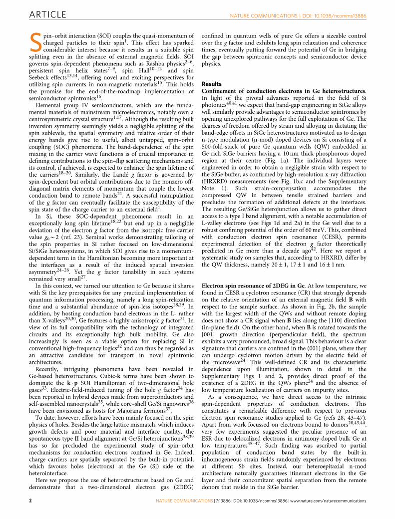
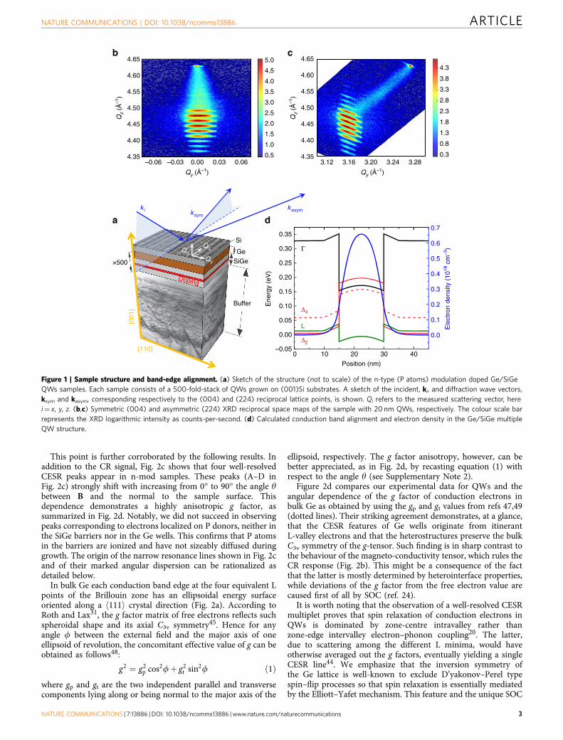
ResultsConfinement of conduction electrons in Ge heterostructures.In light of the pivotal advances reported in the field of Siphotonics40,41 we expect that band-gap engineering in SiGe alloyswill similarly provide advantages to semiconductor spintronics byopening unexplored pathways for the full exploitation of Ge. Thedegrees of freedom offered by strain and alloying in dictating theband-edge offsets in SiGe heterostructures motivated us to designn-type modulation (n-mod) doped devices on Si consisting of a500-fold-stack of pure Ge quantum wells (QW) embedded inGe-rich SiGe barriers having a 10 nm thick phosphorous dopedregion at their centre (Fig. 1a). The individual layers wereengineered in order to obtain a negligible strain with respect tothe SiGe buffer, as confirmed by high-resolution x-ray diffraction(HRXRD) measurements (see Fig. 1b,c and the SupplementaryNote 1). Such strain-compensation accommodates thecompressed QW in between tensile strained barriers andprecludes the formation of additional defects at the interfaces.The resulting Ge/SiGe heterojunction allows us to gather directaccess to a type I band alignment, with a notable accumulation ofL-valley electrons (see Figs 1d and 2a) in the Ge well due to arobust confining potential of the order of 60 meV. This, combinedwith conduction electron spin resonance (CESR), permitsexperimental detection of the electron g factor theoreticallypredicted in Ge more than a decade ago42. Here we report asystematic study on samples that, according to HRXRD, differ bythe QW thickness, namely 20±1, 17±1 and 16±1 nm.
Electron spin resonance of 2DEG in Ge. At low temperature, wefound in CESR a cyclotron resonance (CR) that strongly dependson the relative orientation of an external magnetic field B withrespect to the sample surface. As shown in Fig. 2b, the samplewith the largest width of the QWs and without remote dopingdoes not show a CR signal when B lies along the [110] direction(in-plane field). On the other hand, when B is rotated towards the[001] growth direction (perpendicular field), the spectrumexhibits a very pronounced, broad signal. This behaviour is a clearsignature that carriers are confined in the (001) plane, where theycan undergo cyclotron motion driven by the electric field ofthe microwave24. This well-defined CR and its characteristicdependence upon illumination, shown in detail in theSupplementary Figs 1 and 2, provides direct proof of theexistence of a 2DEG in the QWs plane24 and the absence oflow temperature localization of carriers on impurity sites.
As a consequence, we have direct access to the intrinsicspin-dependent properties of conduction electrons. Thisconstitutes a remarkable difference with respect to previouselectron spin resonance studies applied to Ge (refs 28, 43–47).Apart from work focussed on electrons bound to donors28,43,44,very few experiments suggested the peculiar presence of anESR due to delocalized electrons in antimony-doped bulk Ge atlow temperatures45–47. Such finding was ascribed to partialpopulation of conduction band states by the built-ininhomogeneous strain fields randomly experienced by electronsat different Sb sites. Instead, our heteroepitaxial n-modarchitecture naturally guarantees itinerant electrons in the Gelayer and their concomitant spatial separation from the remotedonors that reside in the SiGe barrier.
ARTICLE NATURE COMMUNICATIONS | DOI: 10.1038/ncomms13886
2 NATURE COMMUNICATIONS | 7:13886 | DOI: 10.1038/ncomms13886 | www.nature.com/naturecommunications
This point is further corroborated by the following results. Inaddition to the CR signal, Fig. 2c shows that four well-resolvedCESR peaks appear in n-mod samples. These peaks (A–D inFig. 2c) strongly shift with increasing from 0� to 90� the angle ybetween B and the normal to the sample surface. Thisdependence demonstrates a highly anisotropic g factor, assummarized in Fig. 2d. Notably, we did not succeed in observingpeaks corresponding to electrons localized on P donors, neither inthe SiGe barriers nor in the Ge wells. This confirms that P atomsin the barriers are ionized and have not sizeably diffused duringgrowth. The origin of the narrow resonance lines shown in Fig. 2cand of their marked angular dispersion can be rationalized asdetailed below.
In bulk Ge each conduction band edge at the four equivalent Lpoints of the Brillouin zone has an ellipsoidal energy surfaceoriented along a h111i crystal direction (Fig. 2a). According toRoth and Lax31, the g factor matrix of free electrons reflects suchspheroidal shape and its axial C3v symmetry45. Hence for anyangle f between the external field and the major axis of oneellipsoid of revolution, the concomitant effective value of g can beobtained as follows48:
g2 ¼ g2p cos2fþ g2
t sin2f ð1Þwhere gp and gt are the two independent parallel and transversecomponents lying along or being normal to the major axis of the
ellipsoid, respectively. The g factor anisotropy, however, can bebetter appreciated, as in Fig. 2d, by recasting equation (1) withrespect to the angle y (see Supplementary Note 2).
Figure 2d compares our experimental data for QWs and theangular dependence of the g factor of conduction electrons inbulk Ge as obtained by using the gp and gt values from refs 47,49(dotted lines). Their striking agreement demonstrates, at a glance,that the CESR features of Ge wells originate from itinerantL-valley electrons and that the heterostructures preserve the bulkC3v symmetry of the g-tensor. Such finding is in sharp contrast tothe behaviour of the magneto-conductivity tensor, which rules theCR response (Fig. 2b). This might be a consequence of the factthat the latter is mostly determined by heterointerface properties,while deviations of the g factor from the free electron value arecaused first of all by SOC (ref. 24).
It is worth noting that the observation of a well-resolved CESRmultiplet proves that spin relaxation of conduction electrons inQWs is dominated by zone-centre intravalley rather thanzone-edge intervalley electron–phonon coupling20. The latter,due to scattering among the different L minima, would haveotherwise averaged out the g factors, eventually yielding a singleCESR line44. We emphasize that the inversion symmetry ofthe Ge lattice is well-known to exclude D’yakonov–Perel typespin–flip processes so that spin relaxation is essentially mediatedby the Elliott–Yafet mechanism. This feature and the unique SOC
[001
]
[110]
×500 SiGe
Ge
Buffer
Si
c
k i ksym
kasym
Qx
Qy
Qz
0 10 20 30 40–0.05
0.00
0.05
0.10
0.15
0.20
0.25
0.30
0.35
L
Δ4
Δ2
Ene
rgy
(eV
)
Position (nm)
Γ
0.0
0.1
0.2
0.3
0.4
0.5
0.6
0.7d
5.0
4.5
4.0
3.5
3.0
2.5
2.0
1.5
1.0
0.5
4.3
3.8
3.3
2.8
2.3
1.8
1.3
0.8
0.3
4.65
4.60
4.55
4.50
4.45
4.40
4.35
4.65
4.60
4.55
4.50
4.45
4.40
4.35
Qy (Å–1) Qy (Å
–1)
Qz
(Å–1
)
Qz
(Å–1
)
Doping
–0.06 –0.03 0.00 0.03 0.06 3.12 3.16 3.20 3.24 3.28
Ele
ctro
n de
nsity
(10
18 c
m–3
)
b
a
Figure 1 | Sample structure and band-edge alignment. (a) Sketch of the structure (not to scale) of the n-type (P atoms) modulation doped Ge/SiGe
QWs samples. Each sample consists of a 500-fold-stack of QWs grown on (001)Si substrates. A sketch of the incident, ki, and diffraction wave vectors,
ksym and kasym, corresponding respectively to the (004) and (224) reciprocal lattice points, is shown. Qi refers to the measured scattering vector, here
i¼ x, y, z. (b,c) Symmetric (004) and asymmetric (224) XRD reciprocal space maps of the sample with 20 nm QWs, respectively. The colour scale bar
represents the XRD logarithmic intensity as counts-per-second. (d) Calculated conduction band alignment and electron density in the Ge/SiGe multiple
QW structure.
NATURE COMMUNICATIONS | DOI: 10.1038/ncomms13886 ARTICLE
NATURE COMMUNICATIONS | 7:13886 | DOI: 10.1038/ncomms13886 | www.nature.com/naturecommunications 3
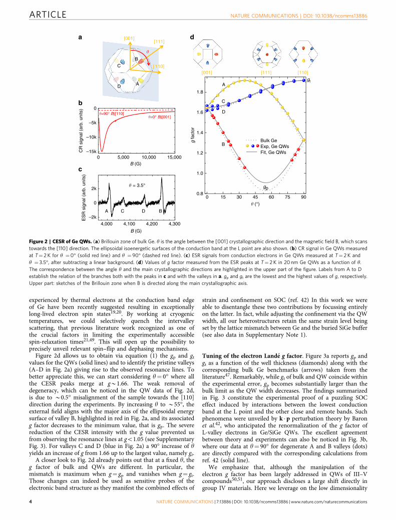
experienced by thermal electrons at the conduction band edgeof Ge have been recently suggested resulting in exceptionallylong-lived electron spin states19,20. By working at cryogenictemperatures, we could selectively quench the intervalleyscattering, that previous literature work recognized as one ofthe crucial factors in limiting the experimentally accessiblespin-relaxation times21,49. This will open up the possibility toprecisely unveil relevant spin–flip and dephasing mechanisms.
Figure 2d allows us to obtain via equation (1) the gp and gt
values for the QWs (solid lines) and to identify the pristine valleys(A–D in Fig. 2a) giving rise to the observed resonance lines. Tobetter appreciate this, we can start considering y¼ 0� where allthe CESR peaks merge at gB1.66. The weak removal ofdegeneracy, which can be noticed in the QW data of Fig. 2d,is due to B0.5� misalignment of the sample towards the [110]direction during the experiments. By increasing y to B55�, theexternal field aligns with the major axis of the ellipsoidal energysurface of valley B, highlighted in red in Fig. 2a, and its associatedg factor decreases to the minimum value, that is gp. The severereduction of the CESR intensity with the g value prevented usfrom observing the resonance lines at go1.05 (see SupplementaryFig. 3). For valleys C and D (blue in Fig. 2a) a 90� increase of yyields an increase of g from 1.66 up to the largest value, namely gt.
A closer look to Fig. 2d already points out that at a fixed y, theg factor of bulk and QWs are different. In particular, themismatch is maximum when g¼ gp and vanishes when g¼ gt.Those changes can indeed be used as sensitive probes of theelectronic band structure as they manifest the combined effects of
strain and confinement on SOC (ref. 42) In this work we wereable to disentangle these two contributions by focussing entirelyon the latter. In fact, while adjusting the confinement via the QWwidth, all our heterostructures retain the same strain level beingset by the lattice mismatch between Ge and the buried SiGe buffer(see also data in Supplementary Note 1).
Tuning of the electron Lande g factor. Figure 3a reports gp andgt as a function of the well thickness (diamonds) along with thecorresponding bulk Ge benchmarks (arrows) taken from theliterature47. Remarkably, while gt of bulk and QW coincide withinthe experimental error, gp becomes substantially larger than thebulk limit as the QW width decreases. The findings summarizedin Fig. 3 constitute the experimental proof of a puzzling SOCeffect induced by interactions between the lowest conductionband at the L point and the other close and remote bands. Suchphenomena were unveiled by k � p perturbation theory by Baronet al.42, who anticipated the renormalization of the g factor ofL-valley electrons in Ge/SiGe QWs. The excellent agreementbetween theory and experiments can also be noticed in Fig. 3b,where our data at y¼ 90� for degenerate A and B valleys (dots)are directly compared with the corresponding calculations fromref. 42 (solid line).
We emphasize that, although the manipulation of theelectron g factor has been largely addressed in QWs of III–Vcompounds50,51, our approach discloses a large shift directly ingroup IV materials. Here we leverage on the low dimensionality
0 15 30 45 60 75 900.8
1.0
1.2
1.4
1.6
1.8
Bulk GeExp, Ge QWsFit, Ge QWs
[110]
�
[001][111]
A
BC
D
4,000 4,100 4,200 4,300–2k
0
2k
0 5,000 10,000 15,000–15k
–10k
–5k
0
CR
sig
nal (
arb.
uni
ts)
ES
R s
igna
l (ar
b. u
nits
)
B
A
C
D
a d
gt
gp
[001] [111] [110]
BA C D
B (G)
B (G)
g fa
ctor
� (°)
� = 3.5°
�=0° B||[001]�=90° B||[110]
b
c
Figure 2 | CESR of Ge QWs. (a) Brillouin zone of bulk Ge. y is the angle between the [001] crystallographic direction and the magnetic field B, which scans
towards the [110] direction. The ellipsoidal isoenergetic surfaces of the conduction band at the L point are also shown. (b) CR signal in Ge QWs measured
at T¼ 2 K for y ¼0� (solid red line) and y ¼90� (dashed red line). (c) ESR signals from conduction electrons in Ge QWs measured at T¼ 2 K and
y ¼ 3.5�, after subtracting a linear background. (d) Values of g factor measured from the ESR peaks at T¼ 2 K in 20 nm Ge QWs as a function of y.
The correspondence between the angle y and the main crystallographic directions are highlighted in the upper part of the figure. Labels from A to D
establish the relation of the branches both with the peaks in c and with the valleys in a. gp and gt are the lowest and the highest values of g, respectively.
Upper part: sketches of the Brillouin zone when B is directed along the main crystallographic axis.
ARTICLE NATURE COMMUNICATIONS | DOI: 10.1038/ncomms13886
4 NATURE COMMUNICATIONS | 7:13886 | DOI: 10.1038/ncomms13886 | www.nature.com/naturecommunications
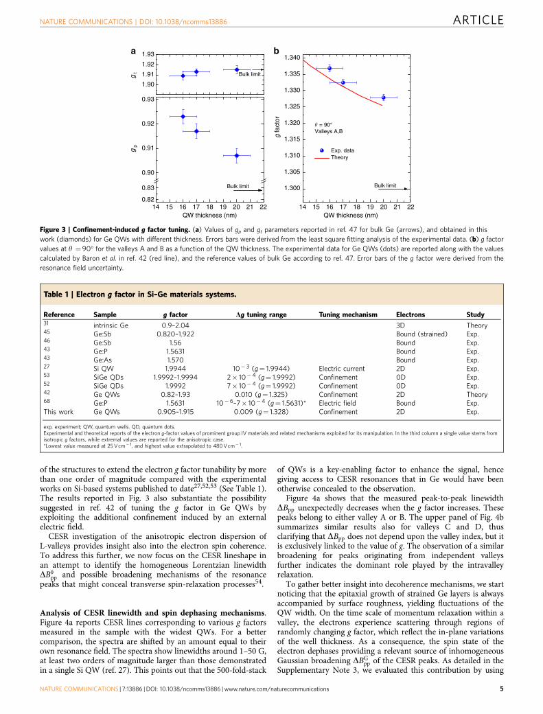
of the structures to extend the electron g factor tunability by morethan one order of magnitude compared with the experimentalworks on Si-based systems published to date27,52,53 (See Table 1).The results reported in Fig. 3 also substantiate the possibilitysuggested in ref. 42 of tuning the g factor in Ge QWs byexploiting the additional confinement induced by an externalelectric field.
CESR investigation of the anisotropic electron dispersion ofL-valleys provides insight also into the electron spin coherence.To address this further, we now focus on the CESR lineshape inan attempt to identify the homogeneous Lorentzian linewidthDB0
pp and possible broadening mechanisms of the resonancepeaks that might conceal transverse spin-relaxation processes54.
Analysis of CESR linewidth and spin dephasing mechanisms.Figure 4a reports CESR lines corresponding to various g factorsmeasured in the sample with the widest QWs. For a bettercomparison, the spectra are shifted by an amount equal to theirown resonance field. The spectra show linewidths around 1–50 G,at least two orders of magnitude larger than those demonstratedin a single Si QW (ref. 27). This points out that the 500-fold-stack
of QWs is a key-enabling factor to enhance the signal, hencegiving access to CESR resonances that in Ge would have beenotherwise concealed to the observation.
Figure 4a shows that the measured peak-to-peak linewidthDBpp unexpectedly decreases when the g factor increases. Thesepeaks belong to either valley A or B. The upper panel of Fig. 4bsummarizes similar results also for valleys C and D, thusclarifying that DBpp does not depend upon the valley index, but itis exclusively linked to the value of g. The observation of a similarbroadening for peaks originating from independent valleysfurther indicates the dominant role played by the intravalleyrelaxation.
To gather better insight into decoherence mechanisms, we startnoticing that the epitaxial growth of strained Ge layers is alwaysaccompanied by surface roughness, yielding fluctuations of theQW width. On the time scale of momentum relaxation within avalley, the electrons experience scattering through regions ofrandomly changing g factor, which reflect the in-plane variationsof the well thickness. As a consequence, the spin state of theelectron dephases providing a relevant source of inhomogeneousGaussian broadening DBG
pp of the CESR peaks. As detailed in theSupplementary Note 3, we evaluated this contribution by using
1.90
1.91
1.92
1.93
14 15 16 17 18 19 20 21 22
Exp. dataTheory
Bulk limit
Bulk limit
Bulk limit
� = 90°Valleys A,B
14 15 16 17 18 19 20 21 22QW thickness (nm) QW thickness (nm)
0.82
0.83
0.90
0.91
0.92
0.93
1.300
1.305
1.310
1.315
1.320
1.325
1.330
1.335
1.340
g fa
ctor
g p
g t
ba
Figure 3 | Confinement-induced g factor tuning. (a) Values of gp and gt parameters reported in ref. 47 for bulk Ge (arrows), and obtained in this
work (diamonds) for Ge QWs with different thickness. Errors bars were derived from the least square fitting analysis of the experimental data. (b) g factor
values at y ¼ 90� for the valleys A and B as a function of the QW thickness. The experimental data for Ge QWs (dots) are reported along with the values
calculated by Baron et al. in ref. 42 (red line), and the reference values of bulk Ge according to ref. 47. Error bars of the g factor were derived from the
resonance field uncertainty.
Table 1 | Electron g factor in Si–Ge materials systems.
Reference Sample g factor Dg tuning range Tuning mechanism Electrons Study31 intrinsic Ge 0.9–2.04 3D Theory45 Ge:Sb 0.820–1.922 Bound (strained) Exp.46 Ge:Sb 1.56 Bound Exp.43 Ge:P 1.5631 Bound Exp.43 Ge:As 1.570 Bound Exp.27 Si QW 1.9944 10� 3 (g¼ 1.9944) Electric current 2D Exp.53 SiGe QDs 1.9992–1.9994 2� 10�4 (g¼ 1.9992) Confinement 0D Exp.52 SiGe QDs 1.9992 7� 10�4 (g¼ 1.9992) Confinement 0D Exp.42 Ge QWs 0.82–1.93 0.010 (g¼ 1.325) Confinement 2D Theory68 Ge:P 1.5631 10�6–7� 10�4 (g¼ 1.5631)* Electric field Bound Exp.This work Ge QWs 0.905–1.915 0.009 (g¼ 1.328) Confinement 2D Exp.
exp, experiment; QW, quantum wells. QD, quantum dots.Experimental and theoretical reports of the electron g-factor values of prominent group IV materials and related mechanisms exploited for its manipulation. In the third column a single value stems fromisotropic g factors, while extremal values are reported for the anisotropic case.*Lowest value measured at 25 Vcm� 1, and highest value extrapolated to 480 Vcm� 1.
NATURE COMMUNICATIONS | DOI: 10.1038/ncomms13886 ARTICLE
NATURE COMMUNICATIONS | 7:13886 | DOI: 10.1038/ncomms13886 | www.nature.com/naturecommunications 5
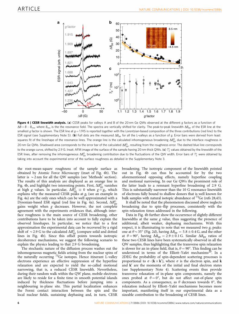
the root-mean-square roughness of the sample surface asobtained by Atomic Force Microscopy (inset of Fig. 4b). Thelatter is B2 nm for all the QW samples (see ‘Methods’ section).The results of this analysis are displayed as an orange line inFig. 4b, and highlight two interesting points. First, DBG
pp vanishesat high g values. In particular, DBG
pp � 0 when g¼ gt, whichexplains why the measured CESR peaks at gt (see an example inFig. 4a) are the only ones which can be well approximated with aDysonian-based ESR signal (red line in Fig. 4a). Second, DBG
ppgains weight when g decreases. However, the not completeagreement with the experiments evidences that, although inter-face roughness is the main source of CESR broadening, othercontributions have to be taken into account to fully explain theobserved lineshapes. In particular, we notice that to a firstapproximation the experimental data can be recovered by a rigidshift of B2.9 G to the calculated DBG
pp (compare solid and dottedlines in Fig. 4b). Since this offset points towards isotropicdecoherence mechanisms, we suggest the following scenario toexplain the physics leading to that 2.9 G broadening.
The stochastic nature of the diffusion process washes out theinhomogeneous magnetic fields arising from the nuclear spins ofthe naturally occurring 73Ge isotopes. Hence itinerant L-valleyelectrons experience an effective suppression of the hyperfinerelaxation and are expected to yield the so-called motionalnarrowing, that is, a reduced CESR linewidth. Nevertheless,during their random walk within the QW plane, mobile electronsare likely to reside for a finite time in smooth potential islandsinduced by thickness fluctuations before jumping into aneighbouring in-plane site. This partial localization enhancesthe Fermi contact interaction between the spin and thelocal nuclear fields, sustaining dephasing and, in turn, CESR
broadening. The isotropic component of the linewidth pointedout in Fig. 4b can thus be accounted for by the twoaforementioned opposing effects, namely hyperfine couplingand motional narrowing. In our Ge QWs the prominent role ofthe latter leads to a remnant hyperfine broadening of 2.9 G.This is substantially narrower than the 10 G resonance linewidthof electrons fully bound to shallow donors that is well known forbulk samples with natural isotopic abundance of 73Ge (refs 28,43).
It shall be noted that the phenomenon discussed above neglectsbroadening due to spin–flip processes, consistently with thespin-relaxation times addressed in the following.
Data in Fig. 4b further show the occurrence of slightly differentlinewidths at the same g value, thus suggesting the presence ofadditional, albeit weaker, dephasing mechanisms. With thisrespect, it is illuminating to note that we measured two gt peaks:one at yB35� (Fig. 2d), having DBpp ¼ 5:8� 0:4 G, and the otherat y¼ 90�, having DBpp ¼ 2:9� 0:1 G. Similar DBpp ratios ofthese two CESR lines have been systematically observed in all theQW samples, thus highlighting that the transverse spin relaxationis slower for an in-plane field, that is, y¼ 90�. This finding can beunderstood in terms of the Elliott–Yafet mechanims20. In a2DEG the probability of spin-dependent scattering processes isproportional to s � (k� k0), where s is the electron spin, and kand k0 are the momenta of the initial and final electron states(see Supplementary Note 4). Scattering events thus providetransverse relaxation of in-plane spin components, namely theones probed at y¼ 0�, but do not affect out-of-plane spincomponents. As a consequence, as y decreases towards 0�, therelaxation induced by Elliott–Yafet mechanisms becomes moreimportant, manifesting itself in our experimental data as asizeable contribution to the broadening of CESR lines.
0
10
20
ΔBpp
(G
)T
2 *
(ns)
30
40
50
60
1.1 1.2 1.3 1.4 1.5 1.6 1.7 1.8 1.9
100
101
102
1.897
1.909
1.688
1.427
1.821
1.643
g factor
–4.5 nm
8.5 nm
10 μm
ES
R s
igna
l (ar
b. u
nits
)
1.236
1.915
g t
500–50ΔB (G)
g factor
ΔBpp
a b
c
Figure 4 | CESR linewidth analysis. (a) CESR peaks for valleys A and B of the 20 nm Ge QWs observed at the different g factors as a function of
DB¼ B� Bres, where Bres is the the resonance field. The spectra are vertically shifted for clarity. The peak-to-peak linewidth DBpp of the ESR line at the
smallest g factor is shown. The ESR line at g¼ 1.915 is reported together with the Lorentzian-based composition of the three contributions (red line) to the
ESR signal (see Supplementary Note 5). (b) Full dots are the measured DBpp for all the L-valleys as a function of g. Error bars were derived from least
squares fit of the lineshape of the resonance lines. The orange line is the calculated inhomogeneous broadening DBGpp due to the interface roughness in
20 nm Ge QWs. Shadowed area corresponds to the error bar of the calculated DBGpp, resulting from the roughness error. The dashed blue line corresponds
to the orange curve, shifted by 2.9 G. Inset: AFM image of the surface of the sample having 20 nm thick QWs. (c) T�2 values obtained by the linewidth of the
ESR lines, after removing the inhomogeneous DBGpp broadening contribution due to the fluctuations of the QW width. Error bars of T�2 were obtained by
taking into account the experimental error of the surface roughness as detailed in the Supplementary Note 3.
ARTICLE NATURE COMMUNICATIONS | DOI: 10.1038/ncomms13886
6 NATURE COMMUNICATIONS | 7:13886 | DOI: 10.1038/ncomms13886 | www.nature.com/naturecommunications
The observation of larger linewidths at small y values also rulesout decoherence due to Rashba SOI. Although precluded by thesymmetric design of our n-mod structures, this effect can stillpossibly occur because of the rotoinversion asymmetry inducedby the finite, unavoidable roughness of the interfaces orasymmetric doping55. The nature of such SOI, if any, wouldlead to a Rashba field oriented within the 2DEG plane3 and wouldprovide an additional channel of transverse spin relaxation that,as opposed to our findings, increases the linewidth when yapproaches 90� (ref. 56).
After having discussed the mechanisms contributing to theobserved CESR linewidth, we can determine the relaxation timeof the spin ensemble T�2 , which provides a lower limit for the spindecoherence time T2 (ref. 54), as follows:
T�2 ¼‘
gmB
2ffiffiffi3p
DB0pp
ð2Þ
where : is the reduced Planck constant, mB the Bohr magneton, gis obtained from the CESR peak position, and DB0
pp can beobtained by the following relation57:
DBpp gð Þ ¼ 12DB0
ppþffiffiffiffiffiffiffiffiffiffiffiffiffiffiffiffiffiffiffiffiffiffiffiffiffiffiffiffiffiffiffiffiffiffiffiffiffiffiffiffiffiffiffiffiffiffi14
DB0pp
h i2þ DBG
pp gð Þh i2r
ð3Þ
using the measured DBpp(g) shown in Fig. 4b, and theinhomogeneous broadenings DBG
pp(g) as calculated in theSupplementary Note 3.
The values of T�2 for the widest QW sample are summarized inFig. 4c. Similar data have been found also for narrower QWs(Supplementary Fig. 4). In agreement with the physical picture ofitinerant electrons subject to fluctuating confinement potentials,T�2 turns out to be about 20 ns, which is about two times longerthan the hyperfine-limited dephasing times of electrons bound to
shallow donors28 and more in line with magneto-optical data forconduction band electrons in bulk Ge (ref. 58). In the latter casethe spin decoherence time was found to be anisotropic, reflectingthe intervalley scattering regime49. Figure 4b demonstrates thatwhen the intravalley relaxation is dominant, the ensembledephasing time is not g-factor-dependent and thus isotropic.
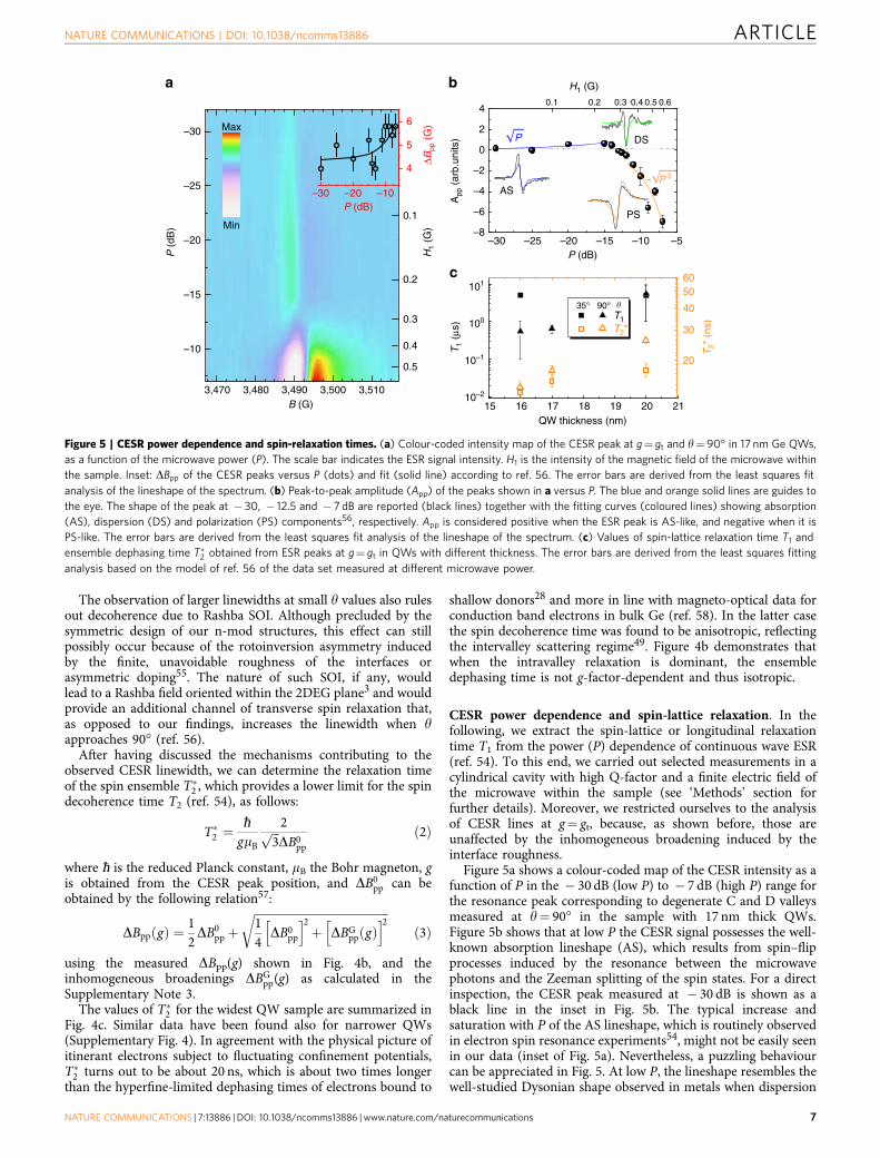
CESR power dependence and spin-lattice relaxation. In thefollowing, we extract the spin-lattice or longitudinal relaxationtime T1 from the power (P) dependence of continuous wave ESR(ref. 54). To this end, we carried out selected measurements in acylindrical cavity with high Q-factor and a finite electric field ofthe microwave within the sample (see ‘Methods’ section forfurther details). Moreover, we restricted ourselves to the analysisof CESR lines at g¼ gt, because, as shown before, those areunaffected by the inhomogeneous broadening induced by theinterface roughness.
Figure 5a shows a colour-coded map of the CESR intensity as afunction of P in the � 30 dB (low P) to � 7 dB (high P) range forthe resonance peak corresponding to degenerate C and D valleysmeasured at y¼ 90� in the sample with 17 nm thick QWs.Figure 5b shows that at low P the CESR signal possesses the well-known absorption lineshape (AS), which results from spin–flipprocesses induced by the resonance between the microwavephotons and the Zeeman splitting of the spin states. For a directinspection, the CESR peak measured at � 30 dB is shown as ablack line in the inset in Fig. 5b. The typical increase andsaturation with P of the AS lineshape, which is routinely observedin electron spin resonance experiments54, might not be easily seenin our data (inset of Fig. 5a). Nevertheless, a puzzling behaviourcan be appreciated in Fig. 5. At low P, the lineshape resembles thewell-studied Dysonian shape observed in metals when dispersion
–30 –25 –20 –15 –10 –5–8
–6
–4
–2
0
2
40.60.50.40.30.20.1
3,470 3,480 3,490 3,500 3,510
–10
–15
–20
–25
–30
0.1
0.2
0.3
0.4
Max
Min
0.5
AS
DS
PS
-
b
c
a
–30 –20 –10
4
5
6
15 16 17 18 19 20 2110–2
10–1
100
101
35°
QW thickness (nm)
20
30
40
5060
P (
dB)
H1
(G)
ΔBpp
(G
)
App
(ar
b.un
its)
P (dB)
T1
(μs)
B (G)
T2*
(ns
)
90° �T1T2*
H1 (G)
P (dB)
P
P 3–
Figure 5 | CESR power dependence and spin-relaxation times. (a) Colour-coded intensity map of the CESR peak at g¼ gt and y¼90� in 17 nm Ge QWs,
as a function of the microwave power (P). The scale bar indicates the ESR signal intensity. H1 is the intensity of the magnetic field of the microwave within
the sample. Inset: DBpp of the CESR peaks versus P (dots) and fit (solid line) according to ref. 56. The error bars are derived from the least squares fit
analysis of the lineshape of the spectrum. (b) Peak-to-peak amplitude (App) of the peaks shown in a versus P. The blue and orange solid lines are guides to
the eye. The shape of the peak at � 30, � 12.5 and � 7 dB are reported (black lines) together with the fitting curves (coloured lines) showing absorption
(AS), dispersion (DS) and polarization (PS) components56, respectively. App is considered positive when the ESR peak is AS-like, and negative when it is
PS-like. The error bars are derived from the least squares fit analysis of the lineshape of the spectrum. (c) Values of spin-lattice relaxation time T1 and
ensemble dephasing time T�2 obtained from ESR peaks at g¼ gt in QWs with different thickness. The error bars are derived from the least squares fitting
analysis based on the model of ref. 56 of the data set measured at different microwave power.
NATURE COMMUNICATIONS | DOI: 10.1038/ncomms13886 ARTICLE
NATURE COMMUNICATIONS | 7:13886 | DOI: 10.1038/ncomms13886 | www.nature.com/naturecommunications 7
of the microwave power arises because of skin effects at the metalsurface54. The pattern is asymmetric because of the occurrence ofan additional dispersion signal (DS), which in 2DEGs wasreported for the first time in Si QWs and explained byconsidering the real component of the magnetic susceptibilityof the samples56. Indeed, by increasing P at first the AS becomesweak and at PB� 12 dB the lineshape gets fully modified,showing one unexpected negative dip, which stems from a pureDS (see also inset of Fig. 5b). Notably, by further increasing P theintensity of the resonance peak turns out to be strongly enhancedand the lineshape changes again showing this time a parityinversion with respect to the AS-like pattern of the low powerregime (see also inset of Fig. 5b). Such sign change of theabsorption component compares well with the polarization signal(PS) occurring in 2D conduction electrons because of variationsof the spin-dependent conductivity during the microwaveabsorption process56.
In light of this discussion, the overall behaviour of the CESRlineshape as a function of P can be accounted for by a linearsuperposition of the three AS, DS and PS contributions(see Supplementary Note 5). According to the model put forwardin ref. 56, the latter leads to a peak-to-peak amplitude App thatscales as
ffiffiffiffiffiP3p
, while AS and DS are both proportional toffiffiffiPp
.Figure 5b, where we assumed negative amplitudes for PS-likepeaks, shows that such a phenomenological power law welldescribes our findings as AS (PS) dominates at low (high) P,while AS and PS cancel each other in the intermediate regime,eventually making the DS component clearly visible atPB� 12 dB.
As detailed in Supplementary Note 5, modelling the resonancelines by these three signal components provides us with the T1
and T�2 times summarized in Fig. 5c for all the QW samples. Forthe sample with the thickest QWs, the model gives T�2 in goodagreement with those anticipated in Fig. 4b for all g factors,further corroborating our previous linewidth analysis. Figure 5calso shows that T�2 decreases and its values at 90� and 35� getcloser in thinner QWs. This behaviour compares well with anenhancement in the electron localization when the QW width isreduced, and with the correspondingly increasing efficiency in thespin dephasing due to hyperfine coupling. Above all, Fig. 5cdiscloses T1 values in the ms regime, thus more than two orders ofmagnitude longer than T�2 . The accuracy of these findings is givenby the analysis of the CESR linewidth reported in Fig. 5a for the17 nm thick QWs. The modelling of the linewidth, as describedin ref. 56, is shown as a solid line in the inset of Fig. 5a andprovides a T1¼ 1 ms, in good agreement with the result of theCESR-amplitude study shown in Fig. 5c.
It is worth noting that spin-lattice relaxation times derived inour QWs approach 5 ms and are substantially longer than theone reported for conduction electrons in bulk Ge at thesame temperatures (see Table 2). While T1 below 1 ms were
experimentally obtained in bulk Ge between 30 and 60 K (ref. 21),in satisfactory agreement with the Elliott–Yafet prediction forthermal electrons20, various attempts failed to recover suchconsistency at lower temperatures (see ref. 29 and refs. therein).In this regime, theory suggests a T1 extending well above the msrange, whilst an experimentally attainable upper bound ofB100 ns was notably singled out at 4 K (ref. 29). All theseendeavours put forward the subtle role played by impurities inintroducing extrinsic spin-relaxation channels59,60 that in bulk Geemerge at low temperatures and drastically prevail over theintrinsic but slower Elliott–Yafet process. By spatially separatingconduction band electrons residing in the Ge QW from theirparent donor atoms embedded in the SiGe barriers, we preventthe impurity-induced bottleneck pertaining to experimentsutilizing bulk Ge wafers, and eventually resolve long-lived spinsdespite the low temperature operation.
In the Orbach-dominated regime, donor-bound electrons havebeen shown to retain in Ge exceedingly long T1 valuesapproaching 100–300ms (ref. 28). Such findings demonstratethat going from itinerant to immobile, fully-localized electrons,while inducing hyperfine dephasing, can be also beneficial inquenching the spin-lattice relaxation activated by impurities andElliott–Yafet spin–flip. This suggests that quantum confinement,guaranteed in our Ge/SiGe heterojunctions by the type I bandalignment, possibly provides an additional mechanism concur-ring to the lengthening of T1 that arises when the conductionelectrons reside in QWs rather than in bulk material.
Optical measurement of T1. To gather a deeper understanding ofthe spin physics offered by the Ge QWs and to substantiatefurther the spin-lattice relaxation times inferred from CESRdata, we carried out time- and polarization-resolved photo-luminescence (PL) measurements (see ‘Methods’ section).
In this case, we leverage spin–orbit to achieve optical spinorientation through absorption of photons carrying angularmomentum. The selection rules for electric dipole interbandtransitions with circularly polarized light allow the excitation of anon-equilibrium population of carriers in the vicinity of theG-point having a net spin orientation along the propagationdirection of the optical beam.
In Ge QWs, the energy relaxation of the photoexcited holes,towards the centre of the Brillouin zone in the valence band, isaccompanied by a quick spin depolarization occurring in a sub psregime61,62. On the other hand, ultrafast scattering events depletethe optically excited conduction band levels on a hundreds-of-fstime scale61,62. Electrons transferred out of G will eventuallyaccumulate at the bottom of the L-valley63, where they reside fora few ns64. The electron spin polarization is notably notextinguished during such non-trivial processes. Finally, it willgovern the radiative recombination with the unpolarizedhole-pocket at G, yielding circularly polarized PL61.
Table 2 | Spin relaxation and dephasing times for electrons in Ge.
Reference Sample T1 (ls) T�2 (ns) T (K) Electrons Technique21 Intrinsic Ge 0.2–0.9 30–60 Cond. - 3D Hot-electron transport58 Intrinsic Ge 0.017–0.065 26–36 10–50 Cond. - 3D Faraday rotation29 Intrinsic Ge 0.127–0.26 4–50 Cond. - 3D Photoluminescence25 Si QWs 2–3 1,400 4–5 Cond. - 2D cw and pulsed ESRThis work Ge QWs 1–5 10–30 2–5 Cond. - 2D cw ESR and PL28 7.8% 73Ge:As 50–800 11 2–5 Bound Pulsed ESR28 0.1% 73Ge:P 10–500 211 0.3–5 Bound Pulsed ESR
cond, conduction; ESR, electron spin resonance; exp, experiment; cw, continuous wave; PL, photoluminescence; QW, quantum wells.Longitudinal relaxation T1 and decoherence time of the spin ensemble T�2 of conduction (cond.) and bound to donor electrons. The samples, the temperature range (T) and the techniques utilized toexperimentally determine the values are also indicated.
ARTICLE NATURE COMMUNICATIONS | DOI: 10.1038/ncomms13886
8 NATURE COMMUNICATIONS | 7:13886 | DOI: 10.1038/ncomms13886 | www.nature.com/naturecommunications
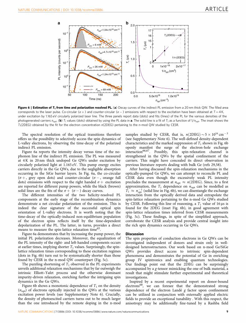
The spectral resolution of the optical transitions thereforeoffers us the possibility to selectively access the spin dynamics ofL-valley electrons, by observing the time-decay of the polarizedindirect PL emission.
Figure 6a reports the intensity decay versus time of the no-phonon line of the indirect PL emission. The PL was measuredat 4 K in 20 nm thick undoped Ge QWs under excitation bycircularly polarized light at 1.165 eV. This pump energy excitescarriers directly in the Ge QWs, due to the negligible absorptionoccurring in the SiGe barrier layers. In Fig. 6a, the co-circular(sþ , grey open dots) and counter-circular (s� , orange fulldots) emissions with respect to the right handed sþ excitationare reported for different pump powers, while the black (brown)solid lines are the fits of the sþ (s� ) decay curves.
The different intensities of the two helicity-resolved PLcomponents at the early stage of the recombination dynamicsdemonstrate a net circular polarization of the emission. This isindeed the clear signature of the successful optical spinorientation of L-valley electrons. It is worth noting that thetime-decay of the optically-induced non-equilibrium populationof the electron spins reflects itself by the time-dependentdepolarization of the PL. The latter, in turns, provides a directmeans to measure the spin-lattice relaxation time65.
Figure 6a demonstrates that by increasing the pump power, theinitial PL polarization decreases. Moreover, the equalization ofthe PL intensity of the right- and left-handed components occursat earlier times, implying shorter T1 values. Surprisingly, the spin-lattice relaxation times corresponding to these excitation regimes(dots in Fig. 6b) turn out to be systematically shorter than thosefound by CESR in the n-mod QW counterpart (Fig. 5c).
The puzzling shortening of T1 observed in the PL experimentsunveils additional relaxation mechanisms that by far outweigh theintrinsic Elliott–Yafet process and the otherwise dominantimpurity-driven relaxation, enriching further the intriguing spindynamics in the Ge QWs.
Figure 6b shows a monotonic dependence of T1 on the density(nopt) of electrons optically injected in the QWs at the variousexcitation power levels (see Supplementary Note 6). Crucially,the density of photoexcited carriers turns out to be much largerthan the one introduced by the remote doping in the n-mod
samples studied by CESR, that is, n 2DEGð Þ� 5� 1016 cm� 3
(see Supplementary Note 6). The well-defined density-dependentcharacteristics and the marked suppression of T1 shown in Fig. 6bopenly manifest the surge of the electron-hole exchangeinteraction66,67. Possibly, this spin-relaxation channel isstrengthened in the QWs by the spatial confinement of thecarriers. This might have concealed its direct observation inprevious literature reports dealing with bulk Ge (refs 29,58).
After having discussed the spin-relaxation mechanisms in theoptically-pumped Ge QWs, we can attempt to reconcile PL andCESR data even though the excessively weak PL intensityprecludes the measurement at nopt n 2DEGð Þ. Since, to a firstapproximation, the T1 dependence on nopt can be modelled asT1 n� 1
opt (solid line in Fig. 6b), we can disentangle the exchangeinteraction from the optically derived data and extrapolate thespin-lattice relaxation pertaining to the n-mod Ge QWs studiedby CESR. Following this line of reasoning, a T1 value of 16 ms isfound for the 2DEG (inset Fig. 6b), in good agreement withspin-lattice relaxation times inferred from CESR measurements(Fig. 5c). These findings, in spite of the simplified approach,corroborate the CESR analysis and provide central insight intothe rich spin dynamics occurring in Ge QWs.
DiscussionThe spin properties of conduction electrons in Ge QWs can beinvestigated independent of donors and strain only in well-designed heterostructures. Our work based on n-mod Ge/SiGeQWs provides direct access to intrinsic spin-dependentphenomena and demonstrates the potential of Ge in enrichinggroup IV spintronics and enabling quantum technologies.Our findings point out that the 2DEG can be surprisinglyaccompanied by a g-tensor mimicking the one of bulk material, aresult that might stimulate further experimental and theoreticalinvestigations.
Inspired by a recent experimental report on donor-boundelectrons68, we can foresee that the demonstrated strongdependence of the electron Lande g factor upon confinementcan be utilized in conjunction with externally applied electricfields to provide an exceptional tunability . With this respect, theanisotropy may be additionally fine-tuned by a Rashba field
00
1
15
16
17
�+�–
ba
1.0
2.0
1.5
0.5
0.0
nopt (cm–3)
50 100 150 200 1.0x10195.0x10180.0
T1
(μs)
10–1
100
10–1
100
10–1
Time (ns)
nopt=1.04×1018 cm–3
Pexc = 6 mW
nopt=4.7×1018 cm–3
Pexc = 26 mW
nopt=1.24×1019 cm–3
Pexc = 69 mW
T1
(μs)
T1(2DEG)
1/n (2DEG)
1/nopt (cm3)
1x10–18 2x10–17
PL
inte
nsity
(co
unts
per
sec
ond)
Figure 6 | Estimation of T1 from time and polarization resolved PL. (a) Decay curves of the indirect PL emission from a 20 nm thick QW. The filled area
corresponds to the laser pulse. Co-circular (sþ ) and counter-circular (s� ) emissions with respect to the excitation have been obtained at T¼4 K,
under excitation by 1.165 eV circularly polarized laser line. The three panels report data (dots) and fits (lines) of the PL for the various densities of the
photogenerated carriers nopt. (b) T1 values (dots) obtained by using the PL data in a. The solid line is a fit of T1 as a function of 1/nopt. The inset shows the
T1(2DEG) obtained by the fit for the electron concentration n(2DEG) pertaining to the n-mod QW studied by CESR.
NATURE COMMUNICATIONS | DOI: 10.1038/ncomms13886 ARTICLE
NATURE COMMUNICATIONS | 7:13886 | DOI: 10.1038/ncomms13886 | www.nature.com/naturecommunications 9
induced by asymmetric doping and subsequently modulated viaan external gate27.
CESR and PL studies unveiled microsecond long spin-latticerelaxation times in the low temperature regime, which strikinglymatch the T1 values measured in Si QWs (refs 25,69). Such resultsheds light on the coexistence of long spin-relaxation times andlarge g factor variations, which support Ge as an excellentcandidate for the exploitation of spin currents in novel transportarchitectures, such as spin-based interconnects70, transistors71
and reprogrammable logic72.We notice that strain engineering and heteroepitaxy on
(111)-oriented substrates have been recently put forward bytheoretical studies19,20,59 as a means to lift the valley degeneracy.Such an approach can be effectively utilized to further lengthenthe spin-lattice relaxation times and extend our results to highertemperatures, in a regime where intervalley scattering providesthe major spin-loss mechanism.
Eventually, by uniquely combining CESR and PL, we were ableto demonstrate the existence of exchange-driven relaxationmechanisms that markedly depend upon the non-equilibriumcarrier density.
Looking ahead, 2DEGs in Ge can offer a special framework forquantum computation, in particular electrostatically defined Gequantum structures on Si can open unexplored pathways forfuture studies of confinement-induced tailoring of the spinphysics in group IV semiconductors.
MethodsSample growth. Ge/SiGe QWs were grown by low energy plasma enhancedchemical vapour deposition73 at 475 �C on p-Si(001) substrates with a resistivity of1–10O cm. Before heteroepitaxy, RCA cleaning was carried out, and the nativeoxide was removed by dipping the substrate in HF solution (HF:H2O 1:10) for 30 s.The first part of the structure consists of a 13 mm thick Si1� xGex graded buffer,deposited at a rate of 5–10 nm s� 1, in which the Ge concentration is linearlyincreased from 0 to 92.5%. A 2 mm thick relaxed Si0.075Ge0.925 layer was depositedon top of the graded buffer. Finally, the stack of 500 pure Ge QWs embedded in21 nm thick Si0.15Ge0.85 barriers was deposited with a rate of 5 nm s� 1. Due toplasma confinement, the growth rate is not uniform across the 400 wafer. For thisreason samples with different QW width but exactly the same stoichiometry of thebarrier layer and comparable strain are provided in one growth run. In the middleof each barrier, co-deposition of P was used to provide a 10 nm layer with Pconcentration of 1011 cm� 2, yielding n-type modulation doping of the QWs.Finally, a 40 nm thick Si0.075Ge0.925 layer and a relaxed crystalline Si capping layerhaving 10 nm of thickness were also deposited.
X-ray diffraction. High-resolution x-ray diffraction measurements wereperformed using a PANalytical X’Pert PRO MRD diffractometer: The system isequipped with a hybrid mirror and a two-bounce asymmetric Ge monochromatorfor a high-intensity Cu Ka1 beam. The beam size in this configuration is2 mm� 20 mm. Reciprocal space maps were taken around the (004) and (224)Bragg reflections. The average Ge content and strain are obtained from the positionof the 0th-order peak in the reciprocal space. The period of the superlattices iscalculated from the satellite peaks period. Composition and thickness of QWand barrier layers are extracted by the intensity profile of the satellites along theout-of-plane component of the scattering vector Qz.
Electronic structure calculation. The band alignment and electronic wavefunctions of the remotely doped QW structures were calculated within the effectivemass approximation by using a Schrodinger–Poisson solver implemented inNextnano74. The set of deformation potentials used for the calculations is reportedin ref. 75 and the average valence band offset between Si and Ge was chosen to be800 meV according to ref. 76.
Atomic force microscopy. We used a Veeco Innova atomic force microscopy(AFM). The microscope was used in tapping mode imaging. We made images of10mm� 10mm area or larger, using a ultra-sharp tip. Samples were rinsed inacetone and isopropanol before carrying out the measurements. AFM images of thesurface of the samples provided a r.m.s. roughness between 1.7±0.2 nm and2.2±0.2 nm.
Electron spin resonance. Two continuous wave EPR spectrometers wereemployed: A Bruker Elexsys E500 with Bruker ER4102ST rectangular cavity
and a Varian E-9 magnet with E-101 microwave bridge (X-band, B9.5 GHz) withsuper-high Q ER4122SHQE cylindrical cavity. Oxford ESR910/ESR900 Liquid Hecryostat operating below 2 and 4 K were used with the two spectrometers,respectively.
Time- and polarization-resolved photoluminescence. PL experiments wereperformed in backscattering geometry using a Nd:YAG Q-switched laser at 10 kHzfrequency, whose pulses have a temporal width of about 10 ns. The circularlypolarized laser light was focused to a 53 mm diameter spot, and the emissionwas probed by a photomultiplier tube (Hamamatsu R5509–73) coupled to amonochromator. The band pass was 3.55 nm, and the time resolution of the wholedetection system 5 ns. The sample was mounted in a cold finger closed-cyclecryostat.
Data availability. The data that support the findings of this study are availablefrom the corresponding authors on request.
References1. Zutic, I., Fabian, J. & Das Sarma, S. Spintronics: fundamentals and applications.
Rev. Mod. Phys. 76, 323–410 (2004).2. Bychkov, Y. A. & Rashba, E. I. Properties of a 2D electron gas with lifted
spectral degeneracy. Z. Eksp. Teor. Fiz. Pis’ma 39, 78–81 (1984).3. Manchon, A., Koo, H. C., Nitta, J., Frolov, S. M. & Duine, R. A. New
perspectives for Rashba spin–orbit coupling. Nat. Mater. 14, 871–882 (2015).4. Bychkov, Y. A. & Rashba, E. I. Oscillatory effects and the magnetic
susceptibility of carriers in inversion layers. J. Phys. C Solid State Phys. 17,6039–6045 (1984).
5. Rashba, E. I. & Sheka, V. I. Symmetry of energy bands in wurzite-type crystals.II. Band symmetry with allowance for spin interactions. Sov. Phys. Solid State 1,143 (1959).
6. Ohkawa, F. J. & Uemura, Y. Quantized surface states of a narrow-gapsemicondutor. J. Phys. Soc. Jpn 37, 1325–1333 (1974).
7. Bernevig, B. A., Orenstein, J. & Zhang, S.-C. Exact SU(2) symmetry andpersistent spin helix in a spin-orbit coupled system. Phys. Rev. Lett. 97, 236601(2006).
8. Koralek, J. D. et al. Emergence of the persistent spin helix in semiconductorquantum wells. Nature 458, 610–613 (2009).
9. Walser, M. P., Reichl, C., Wegscheider, W. & Salis, G. Direct mapping of theformation of a persistent spin helix. Nat. Phys. 8, 757–762 (2012).
10. Dyakonov, M. I. & Perel, V. I. Possibility of orienting electron spins withcurrent. Sov. Phys. JETP Lett. 13, 467 (1971).
11. D’yakonov, M. I. & Perel, V. I. Current-induced spin orientation of electrons insemiconductors. Phys. Lett. A 35, 459–460 (1971).
12. Sinova, J., Valenzuela, S. O., Wunderlich, J., Back, C. H. & Jungwirth, T. SpinHall effects. Rev. Mod. Phys. 87, 1213–1259 (2015).
13. Breton, J.-C. L., Sharma, S., Saito, H., Yuasa, S. & Jansen, R. Thermal spincurrent from a ferromagnet to silicon by Seebeck spin tunnelling. Nature 475,82–85 (2011).
14. Bauer, G. E. W., Saitoh, E. & Wees, B. J. v. Spin caloritronics. Nat. Mater. 11,391–399 (2012).
15. Flatte, M. E. & Awschalom, D. D. Challenges for semiconductor spintronics.Nat. Phys. 3, 153–159 (2007).
16. Jansen, R. Silicon spintronics. Nat. Mater. 11, 400–408 (2012).17. Zutic, I., Fabian, J. & Erwin, S. C. Spin injection and detection in silicon. Phys.
Rev. Lett. 97, 026602 (2006).18. Song, Y. & Dery, H. Analysis of phonon-induced spin relaxation processes in
silicon. Phys. Rev. B 86, 085201 (2012).19. Tang, J.-M., Collins, B. T. & Flatte, M. E. Electron spin-phonon interaction
symmetries and tunable spin relaxation in silicon and germanium. Phys. Rev. B85, 045202 (2012).
20. Li, P., Song, Y. & Dery, H. Intrinsic spin lifetime of conduction electrons ingermanium. Phys. Rev. B 86, 085202 (2012).
21. Li, P., Li, J., Qing, L., Dery, H. & Appelbaum, I. Anisotropy-driven spinrelaxation in germanium. Phys. Rev. Lett. 111, 257204 (2013).
22. Cheng, J. L., Wu, M. W. & Fabian, J. Theory of the spin relaxation ofconduction electrons in silicon. Phys. Rev. Lett. 104, 016601 (2010).
23. Wilson, D. K. & Feher, G. Electron spin resonance experiments on donors insilicon. iii. investigation of excited states by the application of uniaxial stressand their importance in relaxation processes. Phys. Rev. 124, 1068–1083 (1961).
24. Wilamowski, Z., Jantsch, W., Malissa, H. & Roessler, U. Evidence andevaluation of the Bychkov-Rashba effect in SiGe/Si/SiGe quantum wells. Phys.Rev. B 66, 195315 (2002).
25. Tyryshkin, A. M., Lyon, S. A., Jantsch, W. & Schaffler, F. Spin manipulation offree two-dimensional electrons in Si/SiGe quantum wells. Phys. Rev. Lett. 94,126802 (2005).
ARTICLE NATURE COMMUNICATIONS | DOI: 10.1038/ncomms13886
10 NATURE COMMUNICATIONS | 7:13886 | DOI: 10.1038/ncomms13886 | www.nature.com/naturecommunications
26. Matsunami, J., Ooya, M. & Okamoto, T. Electrically detected electron spinresonance in a high-mobility silicon quantum well. Phys. Rev. Lett. 97, 066602(2006).
27. Wilamowski, Z., Hans Malissa, H., Schaeffler, F. & Jantsch, W. g-factor tuningand manipulation of spins by an electric current. Phys. Rev. Lett. 98, 187203(2007).
28. Sigillito, A. J. et al. Electron spin coherence of shallow donors in natural andisotopically enriched. Phys. Rev. Lett. 115, 247601 (2015).
29. Giorgioni, A., Vitiello, E., Grilli, E., Guzzi, M. & Pezzoli, F. Valley-dependentspin polarization and long-lived electron spins in germanium. Appl. Phys. Lett.105, 152404 (2014).
30. Li, P., Trivedi, D. & Dery, H. Spin-dependent optical properties in strainedsilicon and germanium. Phys. Rev. B 87, 115203 (2013).
31. Roth, L. M. & Lax, B. g Factor of electrons in germanium. Phys. Rev. 3, 217–219(1959).
32. Pillarisetty, R. Academic and industry research progress in germaniumnanodevices. Nature 479, 324–328 (2011).
33. Moriya, R. et al. Cubic rashba spin-orbit interaction of a two-dimensional holegas in a strained-Ge/SiGe quantum well. Phys. Rev. Lett. 113, 086601 (2014).
34. Ares, N. et al. Nature of tunable hole g factors in quantum dots. Phys. Rev. Lett.110, 046602 (2013).
35. Katsaros, G. et al. Hybrid superconductor–semiconductor devices made fromself-assembled SiGe nanocrystals on silicon. Nat. Nanotech. 5, 458–464 (2010).
36. Hu, Y., Kuemmeth, F., Lieber, C. M. & Marcus, C. M. Hole spin relaxation inGe–Si core–shell nanowire qubits. Nat. Nanotech. 7, 47–50 (2012).
37. Maier, F., Klinovaja, J. & Loss, D. Majorana fermions in Ge/Si hole nanowires.Phys. Rev. B 90, 195421 (2014).
38. Rieger, M. M. & Vogl, P. Electronic-band parameters in strained Si(1-x)Ge(x)alloys on Si(1-y)Ge(y) substrates. Phys. Rev. B 48, 14276 (1993).
39. Virgilio, M. & Grosso, G. Type-I alignment and direct fundamental gap in SiGebased heterostructures. J. Phys. Condens. Matter 18, 1021–1031 (2006).
40. Kuo, Y.-H. et al. Strong quantum-confined Stark effect in germaniumquantum-well structures on silicon. Nature 437, 1334–1336 (2005).
41. Chaisakul, P. et al. Integrated germanium optical interconnects on siliconsubstrates. Nat. Photon. 8, 482–488 (2014).
42. Baron, F. A. et al. Manipulating the L-valley electron g factor in Si-Geheterostructures. Phys. Rev. B 68, 195306 (2003).
43. Feher, G., Wilson, D. K. & Gere, E. A. Electron spin resonance experiments onshallow donors in germanium. Phys. Rev. Lett. 3, 25–28 (1959).
44. Wilson, D. K. Electron spin resonance experiments on shallow donors ingermanium. Phys. Rev. 134, A265–A286 (1964).
45. Pontinen, R. E. & Sanders, T. M. J. New electron spin resonance spectrum inantimony-doped germanium. Phys. Rev. Lett. 5, 311–313 (1960).
46. Mitsuma, T. & Morigaki, K. Effects of uniaxial [110]-compressive stress onthe additional spin resonance spectrum in Sb-doped Ge. J. Phys. Soc. Jpn. 20,491–499 (1965).
47. Hale, E. B., Dennis, J. R. & Pan, S.-H. Strain effects on the ESR spectrum fromantimony donors in germanium. Phys. Rev. B 12, 2553–2561 (1975).
48. Roth, L. M. g Factor and donor spin-lattice relaxation for electrons ingermanium and silicon. Phys. Rev 118, 1534–1540 (1960).
49. Hautmann, C. & Betz, M. Magneto-optical analysis of the effective g tensorand electron spin decoherence in the multivalley. Phys. Rev. B 85, 121203(R)(2012).
50. Ivchenko, E. L. & Kiselev, A. A. Electron g factor of quantum wells andsuperlattices. Sov. Phys. Semicond. 26, 827–831 (1992).
51. Salis, G., Kato, Y., Ensslin, K., Driscoll, D. C. & Gossard, A. C. Electrical controlof spin coherence in semiconductor nanostructures. Nature 414, 619–622(2001).
52. Zinovieva, A. F. et al. Electron localization in Ge/Si heterostructures withdouble quantum dots detected by an electron spin resonance method. Phys.Rev. B 88, 235308 (2013).
53. Lipps, F. et al. Electron spin resonance study of Si/SiGe quantum dots. Phys.Rev. B 81, 125312 (2010).
54. Poole, C. P. J. Electron Spin Resonance: A Comprehensive Treatise onExperimental Technique (Dover Publications, 1996).
55. Golub, L. E. & Ivchenko, E. L. Spin splitting in symmetrical SiGe quantumwells. Phys. Rev. B 69, 115333 (2004).
56. Wilamowski, Z. & Jantsch, W. Suppression of spin relaxation of conductionelectrons by cyclotron motion. Phys. Rev. B 69, 035328 (2004).
57. Brower, K. L. Strain broadening of the dangling-bond resonance at the(111)Si-Si02 interface. Phys. Rev. B 33, 4471–4478 (1986).
58. Lohrenz, J., Paschen, T. & Betz, M. Resonant spin amplification in intrinsic bulkgermanium: evidence for electron spin lifetimes exceeding 50 ns. Phys. Rev. B89, 121201 (2014).
59. Song, Y., Chalaev, O. & Dery, H. Donor-driven spin relaxation in multivalleysemiconductors. Phys. Rev. Lett. 113, 167201 (2014).
60. Qing, L., Li, J., Appelbaum, I. & Dery, H. Spin relaxation via exchange withdonor impurity-bound electrons. Phys. Rev. B 91, 241405 (R) (2015).
61. Pezzoli, F. et al. Optical spin injection and spin lifetime in Ge heterostructures.Phys. Rev. Lett. 108, 156603 (2012).
62. Lange, C. et al. Spin band-gap renormalization and hole spin dynamics inGe/SiGe quantum wells. Phys. Rev. B 85, 241303(R) (2012).
63. Pezzoli, F. et al. Spin and energy relaxation in germanium studied byspin-polarized direct-gap photoluminescence. Phys. Rev. B 88, 045204 (2013).
64. Giorgioni, A. et al. Photoluminescence decay of direct and indirect transitions inGe/SiGe multiple quantum wells. Appl. Phys. Lett. 111, 013501 (2012).
65. D’yakonov, M. I. Spin Physics in Semiconductors (Springer, 2008).66. Hu, C. et al. Room temperature spin diffusion in (110) GaAs/AlGaAs quantum
wells. Nanoscale Res. Lett. 6, 149 (2011).67. Ohno, Y., Terauchi, R., Adachi, T., Matsukura, F. & Ohno, H. Spin relaxation in
GaAs(110) quantum wells. Phys. Rev. Lett. 83, 4196 (1999).68. Sigillito, A. J. et al. Large stark tuning of donor electron spin quantum bits in
germanium. Phys. Rev. B 94, 125204 (2016).69. Wilamowski, Z. et al. Spin relaxation and g-factor of two-dimensional electrons
in Si/SiGe quantum wells. Physica E 16, 111–120 (2003).70. Dery, H., Song, Y., Li, P. & Zutic, I. Silicon spin communication. Appl. Phys.
Lett. 99, 082502 (2011).71. Datta, S. & Das, B. Electronic analog of the electrooptic modulator. Appl. Phys.
Lett. 56, 665–667 (1990).72. Dery, H., Dalal, P., Cywinski, L. & Sham, L. J. Spin-based logic in
semiconductors for reconfigurable large-scale circuits. Nature 447, 573–576(2007).
73. Rosenblad, C. et al. Silicon epitaxy by low-energy plasma enhanced chemicalvapor deposition. J. Vac. Sci. Technol. A 16, 2785–2790 (1998).
74. Birner, S. et al. Nextnano: general purpose 3-D simulations. TEEE Trans.Electron Devices 54, 2137–2142 (2007).
75. Paul, D. J. 8-band k.p modeling of the quantum confined Stark effect in Gequantum wells on Si substrates. Phys. Rev. B 77, 155323 (2008).
76. Teherani, J. T. et al. Extraction of large valence-band energy offsets andcomparison to theoretical values for strained-Si/strained-Ge type-IIheterostructures on relaxed SiGe substrates. Phys. Rev. B 85, 205308 (2012).
AcknowledgementsWe acknowledge T. Maggi and S. Bietti for assistance with the AFM measurements,L. Golub, M.M. Glazov and M. Guzzi for fruitful discussions. This work was supportedby the Fondazione Cariplo through Grant SearchIV No 2013-0623.
Author contributionsF.P. conceived and coordinated the project, A.G. and S.P. carried out the ESR mea-surements under the supervision of W.J. and M.F.; AFM analysis was conducted by A.G.;x-ray characterization was done by S.C.; E.V. and A.G. performed the PL investigationsunder the supervision of E.G. and F.P.; S.C. and G.I. grew the samples and G.I. carriedout the band structure calculations; all authors discussed the results and commented onthe manuscript written by A.G. and F.P.
Additional informationSupplementary Information accompanies this paper at http://www.nature.com/naturecommunications
Competing financial interests: The authors declare no competing financial interests.
Reprints and permission information is available online at http://npg.nature.com/reprintsandpermissions/
How to cite this article: Giorgioni, A. et al. Strong confinement-induced engineeringof the g factor and lifetime of conduction electron spins in Ge quantum wells.Nat. Commun. 7, 13886 doi: 10.1038/ncomms13886 (2016).
Publisher’s note: Springer Nature remains neutral with regard to jurisdictional claims inpublished maps and institutional affiliations.
This work is licensed under a Creative Commons Attribution 4.0International License. The images or other third party material in this
article are included in the article’s Creative Commons license, unless indicated otherwisein the credit line; if the material is not included under the Creative Commons license,users will need to obtain permission from the license holder to reproduce the material.To view a copy of this license, visit http://creativecommons.org/licenses/by/4.0/
r The Author(s) 2016
NATURE COMMUNICATIONS | DOI: 10.1038/ncomms13886 ARTICLE
NATURE COMMUNICATIONS | 7:13886 | DOI: 10.1038/ncomms13886 | www.nature.com/naturecommunications 11