Embed Size (px)
Citation preview

1
Strong band kinks in magic-thickness Yb films arising from
interfacial electron-phonon coupling
Yi Wu1, Yuan Fang1, Shuyi Zhou1, Peng Li1, Zhongzheng Wu1, Zhiguang Xiao1, Xiaoxiong
Wang2, Chao Cao3, Tai-Chang Chiang4*, Yang Liu1,5,6*
1Center for Correlated Matter and Department of Physics, Zhejiang University, Hangzhou, P. R.
China
2College of Science, Nanjing University of Science and Technology, Nanjing, P. R. China
3Department of Physics, Hangzhou Normal University, Hangzhou, P. R. China
4Department of Physics and Frederick Seitz Material Research Laboratory, University of Illinois
at Urbana-Champaign, Urbana, IL 61822, USA
5Zhejiang Province Key Laboratory of Quantum Technology and Device, Zhejiang University,
Hangzhou, P. R. China
6Collaborative Innovation Center of Advanced Microstructures, Nanjing University, Nanjing, P.
R. China
*Corresponding authors: [email protected], [email protected]

2
Abstract
Interfacial electron-phonon coupling in ultrathin films has attracted much interest; it can give rise
to novel effects and phenomena, including enhanced superconductivity. Here we report an
observation of strong kinks in the energy dispersions of quantum well states in ultrathin Yb films
grown on graphite. These kinks, arising from interfacial electron-phonon coupling, are most
prominent for films with a preferred ("magic") thickness of 4 monolayers, which are strained and
hole doped by the substrate. The energy position of the kinks agrees well with the optical phonon
energy of graphite, and the extracted electron-phonon coupling strength λ shows a large subband
dependence, with a maximum value up to 0.6. The kinks decay rapidly with increasing film
thickness, consistent with its interfacial origin. The variation of λ is correlated with evolution of
the electronic wave function amplitudes at the interface. A Lifshitz transition occurs just beyond
the magic thickness where the heavy Yb 5d bands begin to populate right below the Fermi level.
3
Electron-phonon coupling (EPC) plays an important role in condensed matter physics; it can
drive superconductivity (SC) and charge-density-wave formation [1]. While EPC effects in bulk
materials have been studied extensively, much less is known about interfacial EPC. Because of
abrupt changes of the crystal potential at an interface [2], EPC at the interface can be much stronger
than that in the bulk, possibly leading to enhanced properties in ultrathin films. A notable example
is single-layer FeSe grown on SrTiO3(001), for which a SC transition temperature (TC) up to 60 K
has been reported [3,4,5,6,7,8]. This single-layer TC is almost an order of magnitude higher than
the TC of ~8 K in bulk FeSe. This remarkable effect has been attributed to a large interfacial EPC
[9, 10,11,12, 13], and it points to a promising avenue towards achieving high TC's in interface-
engineered systems [14].
Experimental signatures of interfacial EPC in thin films have been identified by angle-
resolved photoemission spectroscopy (ARPES) via shake-off bands due to bosonic excitations [9]
or temperature-dependent broadening of quasiparticle bands [2]. Theoretically, when the substrate
phonon energy is much smaller than the film conduction band width, interfacial EPC can also give
rise to kinks in the film quasiparticle dispersions [15], similar to those observed in bulk crystals
such as certain cuprates [16,17,18] or in simple metal surfaces [19,20]. However, to the best of our
knowledge, no such interface-EPC-induced kinks for films have been documented in the literature
thus far. Here we report prominent kinks for the quantum well states (QWSs) in ultrathin Yb films
grown on graphite, which imply a strong interfacial EPC in this system. Our extracted coupling
constant λ in the Yb films is as high as 0.6, which far exceeds the Bardeen-Cooper-Schrieffer (BCS)
threshold for SC. It is interesting to note that both Yb and graphite are non-superconducting and
exhibit a weak EPC in the bulk [21].
4
Our work on Yb films is also motivated by earlier studies suggesting that 4f electrons might
be involved in the Fermi surface (FS) of ultrathin Yb films at low temperatures [22], analogous to
the celebrated α phase of Ce [23,24]. Our results for Yb films on graphite demonstrate that the Yb
4f electrons remain localized and do not contribute to the FS. A heavy electron band just below
the Fermi level, with effective mass up to 19 me, is observed for thick films and is attributed to the
Yb 5d states. Prior studies of Yb films on W(110) [25,26,27], while informative, did not provide
the fine band dispersions near the Fermi level to address the issues of 4f-5d occupancy and
interfacial EPC effects.
Yb films were grown by molecular beam epitaxy (MBE) in an Omicron Lab10 growth
chamber. ARPES measurements were performed by transferring the sample under ultrahigh
vacuum from the growth chamber to a dedicated ARPES chamber. ARPES measurements were
performed at ~20 K, using a Scienta-Omicron VUV-5k helium lamp and DA-30(L) electron
analyzer. Most of the ARPES data were taken using He-II photons (40.8 eV), with an energy
(momentum) resolution of ~10 meV (~0.01 Å-1) (see [28] for details).
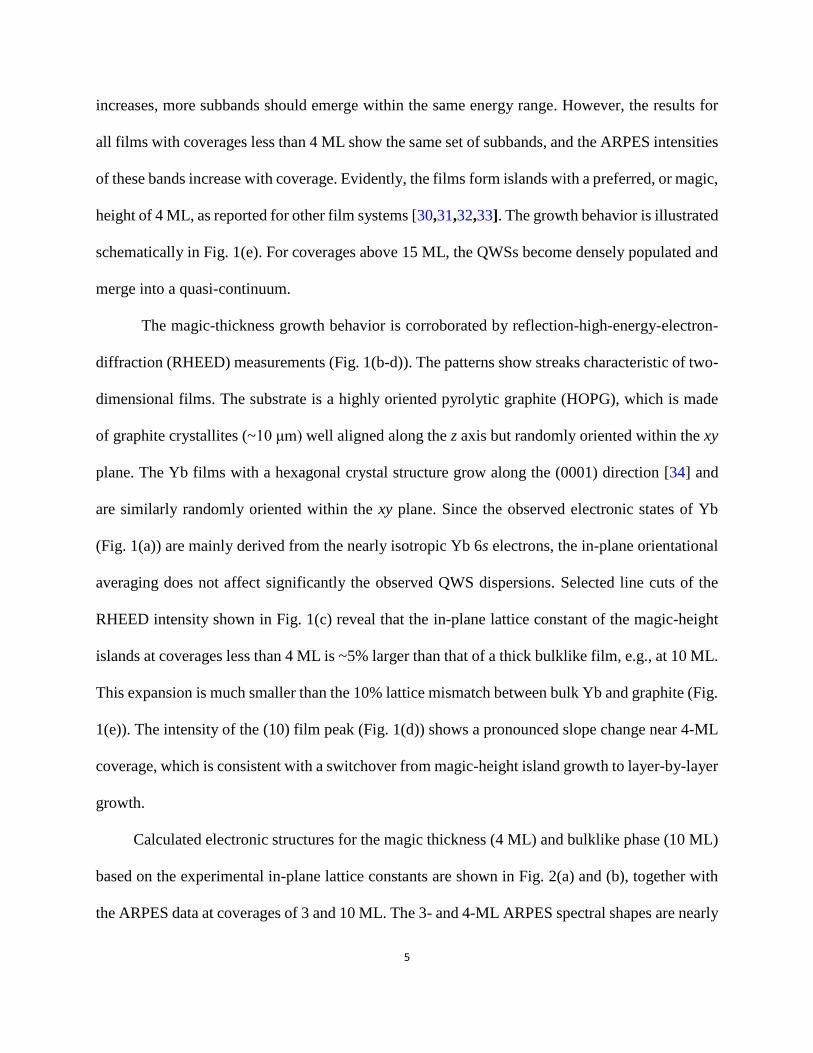
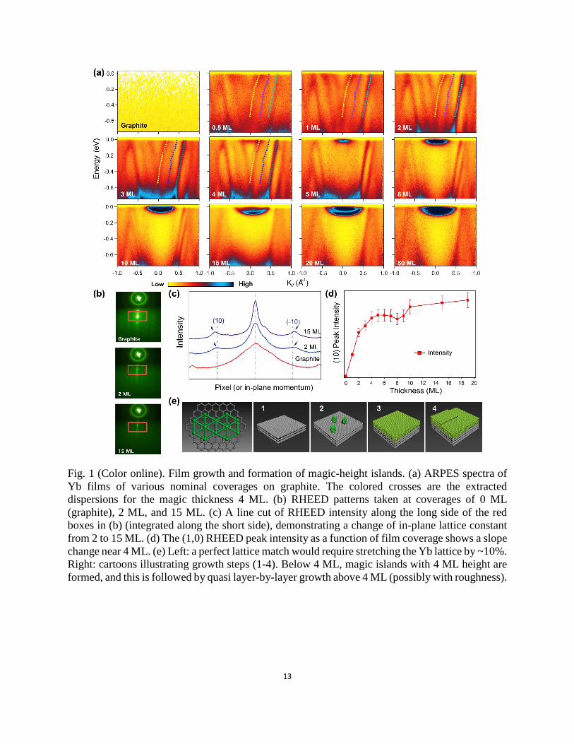
ARPES spectra for Yb films at various coverages, in units of monolayers (MLs), are shown
in Fig. 1(a). The substrate graphite has no occupied bands or features within the probed energy
and momentum ranges. Approximately parabolic bands emerge as the coverage increases; these
correspond to QWSs [29]. The energies of these QWSs are governed by the Bohr-Sommerfeld
quantization condition [29]
2𝑘𝑧(𝐸)𝑁𝑡 + 𝜑𝑠 + 𝜑𝑖 = 2𝑛𝜋, (1)
where kz(E) is the perpendicular momentum as a function of energy E in accordance with the bulk
band structure, N is the film thickness in units of ML, t is the thickness of one ML, φs (φi) is the
phase shift at the surface (interface), and n is the quantum number of each QWS subband. As N
5
increases, more subbands should emerge within the same energy range. However, the results for
all films with coverages less than 4 ML show the same set of subbands, and the ARPES intensities
of these bands increase with coverage. Evidently, the films form islands with a preferred, or magic,
height of 4 ML, as reported for other film systems [30,31,32,33]. The growth behavior is illustrated
schematically in Fig. 1(e). For coverages above 15 ML, the QWSs become densely populated and
merge into a quasi-continuum.
The magic-thickness growth behavior is corroborated by reflection-high-energy-electron-
diffraction (RHEED) measurements (Fig. 1(b-d)). The patterns show streaks characteristic of two-
dimensional films. The substrate is a highly oriented pyrolytic graphite (HOPG), which is made
of graphite crystallites (~10 μm) well aligned along the z axis but randomly oriented within the xy
plane. The Yb films with a hexagonal crystal structure grow along the (0001) direction [34] and
are similarly randomly oriented within the xy plane. Since the observed electronic states of Yb
(Fig. 1(a)) are mainly derived from the nearly isotropic Yb 6s electrons, the in-plane orientational
averaging does not affect significantly the observed QWS dispersions. Selected line cuts of the
RHEED intensity shown in Fig. 1(c) reveal that the in-plane lattice constant of the magic-height
islands at coverages less than 4 ML is ~5% larger than that of a thick bulklike film, e.g., at 10 ML.
This expansion is much smaller than the 10% lattice mismatch between bulk Yb and graphite (Fig.
1(e)). The intensity of the (10) film peak (Fig. 1(d)) shows a pronounced slope change near 4-ML
coverage, which is consistent with a switchover from magic-height island growth to layer-by-layer
growth.
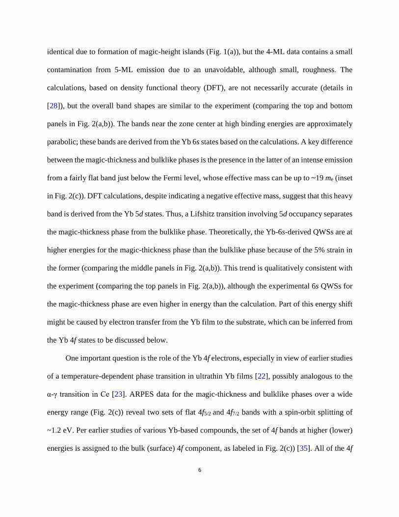
Calculated electronic structures for the magic thickness (4 ML) and bulklike phase (10 ML)
based on the experimental in-plane lattice constants are shown in Fig. 2(a) and (b), together with
the ARPES data at coverages of 3 and 10 ML. The 3- and 4-ML ARPES spectral shapes are nearly
6
identical due to formation of magic-height islands (Fig. 1(a)), but the 4-ML data contains a small
contamination from 5-ML emission due to an unavoidable, although small, roughness. The
calculations, based on density functional theory (DFT), are not necessarily accurate (details in
[28]), but the overall band shapes are similar to the experiment (comparing the top and bottom
panels in Fig. 2(a,b)). The bands near the zone center at high binding energies are approximately
parabolic; these bands are derived from the Yb 6s states based on the calculations. A key difference
between the magic-thickness and bulklike phases is the presence in the latter of an intense emission
from a fairly flat band just below the Fermi level, whose effective mass can be up to ~19 me (inset
in Fig. 2(c)). DFT calculations, despite indicating a negative effective mass, suggest that this heavy
band is derived from the Yb 5d states. Thus, a Lifshitz transition involving 5d occupancy separates
the magic-thickness phase from the bulklike phase. Theoretically, the Yb-6s-derived QWSs are at
higher energies for the magic-thickness phase than the bulklike phase because of the 5% strain in
the former (comparing the middle panels in Fig. 2(a,b)). This trend is qualitatively consistent with
the experiment (comparing the top panels in Fig. 2(a,b)), although the experimental 6s QWSs for
the magic-thickness phase are even higher in energy than the calculation. Part of this energy shift
might be caused by electron transfer from the Yb film to the substrate, which can be inferred from
the Yb 4f states to be discussed below.
One important question is the role of the Yb 4f electrons, especially in view of earlier studies
of a temperature-dependent phase transition in ultrathin Yb films [22], possibly analogous to the
α-γ transition in Ce [23]. ARPES data for the magic-thickness and bulklike phases over a wide
energy range (Fig. 2(c)) reveal two sets of flat 4f5/2 and 4f7/2 bands with a spin-orbit splitting of
~1.2 eV. Per earlier studies of various Yb-based compounds, the set of 4f bands at higher (lower)
energies is assigned to the bulk (surface) 4f component, as labeled in Fig. 2(c)) [35]. All of the 4f
7
bands are far away from the Fermi level, corresponding to an electronic configuration of 4f14 for
both phases. Thus, valence fluctuations involving the 4f13 configuration are irrelevant in the present
case. A 4f13 Yb ion is expected to exhibit characteristic multiple peaks between -6 and -12 eV [36],
which are not observed here. The bulk 4f states for the magic thickness are at slightly higher
energies than those for the bulklike phase. This is consistent with a charge transfer across the
interface that moves the QWSs toward higher energies as discussed earlier.
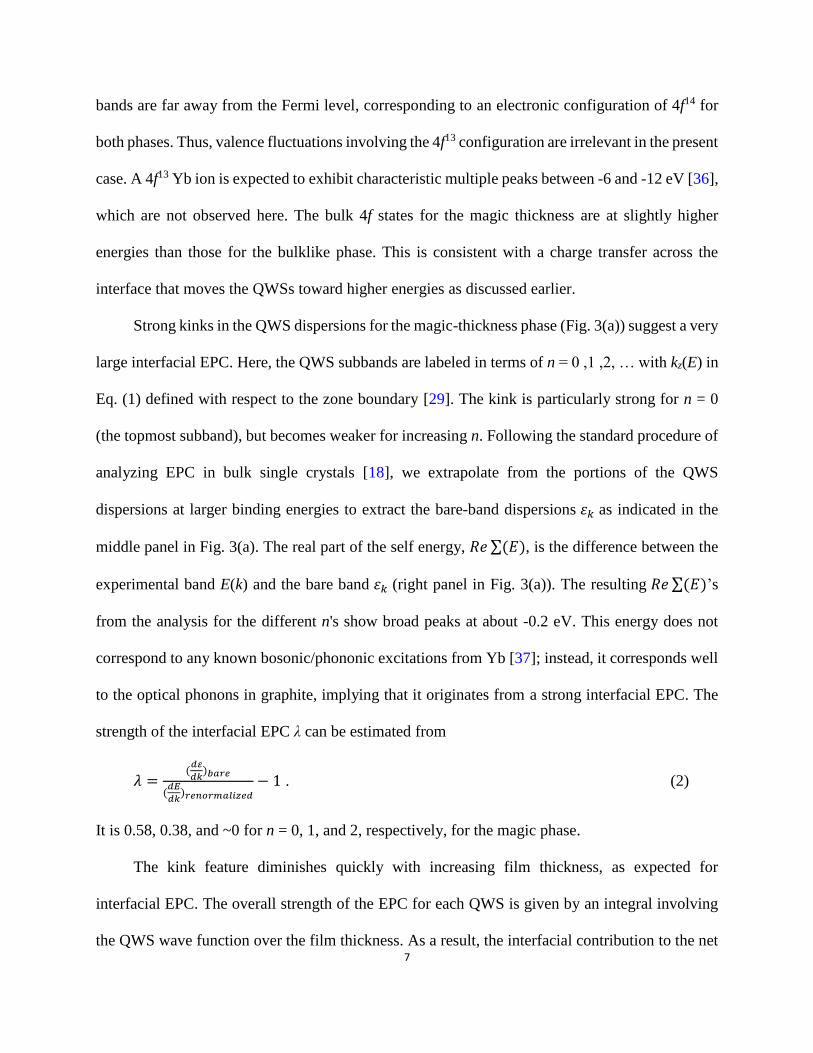
Strong kinks in the QWS dispersions for the magic-thickness phase (Fig. 3(a)) suggest a very
large interfacial EPC. Here, the QWS subbands are labeled in terms of n = 0 ,1 ,2, … with kz(E) in
Eq. (1) defined with respect to the zone boundary [29]. The kink is particularly strong for n = 0
(the topmost subband), but becomes weaker for increasing n. Following the standard procedure of
analyzing EPC in bulk single crystals [18], we extrapolate from the portions of the QWS
dispersions at larger binding energies to extract the bare-band dispersions 𝜀𝑘 as indicated in the
middle panel in Fig. 3(a). The real part of the self energy, 𝑅𝑒∑(𝐸), is the difference between the
experimental band E(k) and the bare band 𝜀𝑘 (right panel in Fig. 3(a)). The resulting 𝑅𝑒∑(𝐸)’s
from the analysis for the different n's show broad peaks at about -0.2 eV. This energy does not
correspond to any known bosonic/phononic excitations from Yb [37]; instead, it corresponds well
to the optical phonons in graphite, implying that it originates from a strong interfacial EPC. The
strength of the interfacial EPC λ can be estimated from
𝜆 =(𝑑𝜀
𝑑𝑘)𝑏𝑎𝑟𝑒
(𝑑𝐸
𝑑𝑘)𝑟𝑒𝑛𝑜𝑟𝑚𝑎𝑙𝑖𝑧𝑒𝑑
− 1 . (2)
It is 0.58, 0.38, and ~0 for n = 0, 1, and 2, respectively, for the magic phase.
The kink feature diminishes quickly with increasing film thickness, as expected for
interfacial EPC. The overall strength of the EPC for each QWS is given by an integral involving
the QWS wave function over the film thickness. As a result, the interfacial contribution to the net
8
EPC must decrease with increasing film thickness [2]. Results of a similar analysis as above for
10 and 20-ML films are shown in Fig. 3(b). The extracted values of λ for the n = 0 QWS is ~0.22
and ~0 for N = 10 and 20 films, respectively. Note that 𝑅𝑒∑(𝐸) for the N = 10 film is also peaked
at about -0.2 eV, consistent with interfacial EPC, but the kink is much weaker.
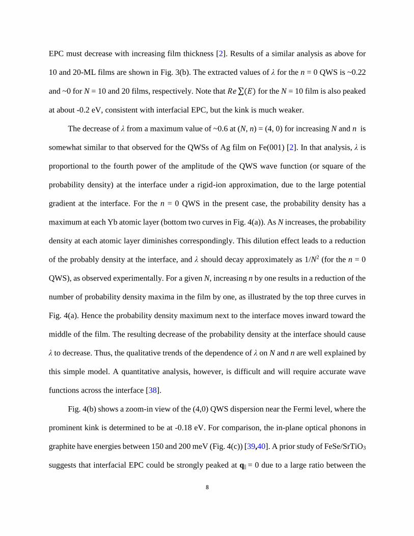
The decrease of λ from a maximum value of ~0.6 at (N, n) = (4, 0) for increasing N and n is
somewhat similar to that observed for the QWSs of Ag film on Fe(001) [2]. In that analysis, λ is
proportional to the fourth power of the amplitude of the QWS wave function (or square of the
probability density) at the interface under a rigid-ion approximation, due to the large potential
gradient at the interface. For the n = 0 QWS in the present case, the probability density has a
maximum at each Yb atomic layer (bottom two curves in Fig. 4(a)). As N increases, the probability
density at each atomic layer diminishes correspondingly. This dilution effect leads to a reduction
of the probably density at the interface, and λ should decay approximately as 1/N2 (for the n = 0
QWS), as observed experimentally. For a given N, increasing n by one results in a reduction of the
number of probability density maxima in the film by one, as illustrated by the top three curves in
Fig. 4(a). Hence the probability density maximum next to the interface moves inward toward the
middle of the film. The resulting decrease of the probability density at the interface should cause
λ to decrease. Thus, the qualitative trends of the dependence of λ on N and n are well explained by
this simple model. A quantitative analysis, however, is difficult and will require accurate wave
functions across the interface [38].
Fig. 4(b) shows a zoom-in view of the (4,0) QWS dispersion near the Fermi level, where the
prominent kink is determined to be at -0.18 eV. For comparison, the in-plane optical phonons in
graphite have energies between 150 and 200 meV (Fig. 4(c)) [39,40]. A prior study of FeSe/SrTiO3
suggests that interfacial EPC could be strongly peaked at q|| = 0 due to a large ratio between the
9
in- and out-of-plane dielectric constants in two-dimensional films [9,41]. The same argument
could apply in the present case. The kink energy of -0.18 eV corresponds well to a weighted
average of the in-plane optical phonons near the Γ and A points (green dashed circles in Fig. 4(c)).
No kinks arising from other lower-energy phonons could be identified, indicating that couplings
to these phonons might be much weaker.
The large interfacial EPC in the magic-thickness phase could be connected to the strain and
possible charge transfer at the Yb/graphite interface. This implies strong interfacial bonding, likely
caused by the small electronegativity of Yb. Similar interfacial charge transfer and strain effect
have been observed in FeSe/SrTiO3 [3], where λ decays rapidly with N and becomes negligibly
small beyond 2 unit cells [9]. In the Yb/graphite case, however, large interfacial EPC occurs for a
magic thickness of 4 ML and decays more gradually with thickness, similar to the Ag/Fe(001) case
[2]. The different thickness dependence of λ may be related to electronic wave mixing or phonon
propagation across the interface.
The above discussion leads to the conclusion that the very strong kinks observed for some
of the Yb QWSs are caused by an interfacial EPC effect that involves coupling of electrons in the
Yb film and the in-plane optical phonons in the graphite substrate. This cross-interface fermion-
boson interaction is strongest for a magic thickness of 4 ML and for the n = 0 QWS, which has the
largest interfacial weight of the wave function. The magic thickness marks the boundary of a
Lifshitz transition with Yb 5d occupancy at larger film thicknesses. The 4f electrons apparently do
not play an important role in these changes. All of these observations indicate that the Yb/graphite
system is highly unusual with remarkable properties that are governed by multiple effects
including quantum confinement, strain, electronic phase transition, and interfacial EPC.
10
This work is supported by the National Key R&D Program of the MOST of China (Grant
No. 2016YFA0300203, 2017YFA0303100) and the National Science Foundation of China (No.
11674280). TCC acknowledges support from the US Department of Energy under Grant No. DE-
FG02-07ER46383. XXW acknowledges support from the Fundamental Research Funds for the
Central Universities (No. 30917011338).
Reference
1 G. Grimvall, The electron-phonon interaction in metals, vol.16 (North-Holland Amsterdam,
1981).
2 D. A. Luh, T. Miller, J. J. Paggel, and T.-C. Chiang, Physical review letters 88, 256802 (2002).
3 Q. Y. Wang et al., Chinese Physics Letters 29, 037402 (2012).
4 D. Liu et al., Nature communications 3, 931 (2012).
5 W. H. Zhang et al., Chinese Physics Letters 31, 017401 (2014).
6 R. Peng et al., Nature communications 5, 5044 (2014).
7 R. Peng et al., Physical review letters 112, 107001 (2014).
8 J. F. Ge, Z. L. Liu, C. Liu, C. L. Gao, D. Qian, Q. K. Xue, Y. Liu, and J. F. Jia, Nature materials
14, 285 (2015).
9 J. J. Lee et al., Nature 515, 245 (2014).
10 H. Ding, Y. F. Lv, K. Zhao, W. L. Wang, L. Wang, C. L. Song, X. Chen, X. C. Ma, and Q. K.
Xue, Physical review letters 117, 067001 (2016).
11 S. Zhang et al., Physical Review B 94 (2016).
12 S. N. Rebec, T. Jia, C. Zhang, M. Hashimoto, D. H. Lu, R. G. Moore, and Z. X. Shen, Physical
review letters 118, 067002 (2017).

11
13 Q. Song et al., Nature communications 10, 758 (2019).
14 I. Bozovic and C. Ahn, Nature Physics 10, 892 (2014).
15 F. Giustino, Reviews of Modern Physics 89, 015003 (2017).
16 T. Valla, A. V. Fedorov, P. D. Johnson, B. O. Wells, S. L. Hulbert, Q. Li, G. D. Gu, and N.
Koshizuka, Science 285, 2110 (1999).
17 A. Lanzara et al., Nature 412, 510 (2001).
18 A. Damascelli, Z. Hussain, and Z.-X. Shen, Reviews of Modern Physics 75, 473 (2003).
19 B. A. McDougall, T. Balasubramanian, and E. Jensen, Physical Review B 51, 13891 (1995).
20 E. W. Plummer, J. Shi, S. J. Tang, E. Rotenberg, and S. D. Kevan, Progress in Surface Science
74, 251 (2003).
21 G. Profeta, M. Calandra, and F. Mauri, Nature Physics 8, 131 (2012).
22 E. Weschke et al., Physical review letters 83, 584 (1999).
23 D. C. Koskenmaki, and Jr K. A. Gschneidner, in Handbook on the Physics and Chemistry of
Rare Earths, Vol.1 (eds Gschneidner, Jr K. A. & Eyring, L.) Ch.4 337-377 (Elsevier, Amsterdam,
North Holland, 1978).
24 J. W. Allen and R. M. Martin, Physical review letters 49, 1106 (1982).
25 D. Wegner, A. Bauer, and G. Kaindl, Physical review letters 94, 126804 (2005).
26 Y. S. Dedkov, D. V. Vyalikh, M. Weser, M. Holder, S. L. Molodtsov, C. Laubschat, Y.
Kucherenko, and M. Fonin, Surface Science 604, 269 (2010).
27 F. Offi et al., Physical Review B 85, 115108 (2012).
28 See supplementary materials.
29 T.-C. Chiang, Surface Science Reports 39, 181 (2000).
30 Z. Zhang., Q. Niu., and C.-K. Shih., Physical review letters 80, 5381 (1998).

12
31 L. Gavioli, K. R. Kimberlin, M. C. Tringides, J. F. Wendelken, and Z. Zhang, Physical review
letters 82, 129 (1999).
32 H. Hong, C. M. Wei, M. Y. Chou, Z. Wu, L. Basile, H. Chen, M. Holt, and T. C. Chiang,
Physical review letters 90, 076104 (2003).
33 Y. Liu, T. Miller, and T.-C. Chiang, Journal of physics. Condensed Matter 23, 365302 (2011).
34 F. X. Kayser, Physical review letters 25, 662 (1970).
35 S. Danzenbächer et al., Physical Review B 75, 045109 (2007).
36 S. Fujimori, Journal of physics. Condensed matter : an Institute of Physics journal 28, 153002
(2016).
37 X. J. Zhang and C. L. Chen, Journal of Low Temperature Physics 169, 40 (2012).
38 N. J. Speer, S. J. Tang, T. Miller, and T.-C. Chiang, Science 314, 804 (2006).
39 M. Mohr, J. Maultzsch, E. Dobardžić, S. Reich, I. Milošević, M. Damnjanović, A. Bosak, M.
Krisch, and C. Thomsen, Physical Review B 76, 035439 (2007).
40 A. Grüneis et al., Physical Review B 80, 085423 (2009).
41 D. H. Lee, Chinese Physics B 24, 117405 (2015).
13
Fig. 1 (Color online). Film growth and formation of magic-height islands. (a) ARPES spectra of
Yb films of various nominal coverages on graphite. The colored crosses are the extracted
dispersions for the magic thickness 4 ML. (b) RHEED patterns taken at coverages of 0 ML
(graphite), 2 ML, and 15 ML. (c) A line cut of RHEED intensity along the long side of the red
boxes in (b) (integrated along the short side), demonstrating a change of in-plane lattice constant
from 2 to 15 ML. (d) The (1,0) RHEED peak intensity as a function of film coverage shows a slope
change near 4 ML. (e) Left: a perfect lattice match would require stretching the Yb lattice by ~10%.
Right: cartoons illustrating growth steps (1-4). Below 4 ML, magic islands with 4 ML height are
formed, and this is followed by quasi layer-by-layer growth above 4 ML (possibly with roughness).

14
Fig. 2 (Color online). Thickness-dependent electronic structure of Yb films. (a,b). ARPES spectra
(top panels) of the magic-height islands (3 ML coverage, a) and the bulk phase (10 ML, b), in
comparison with DFT calculations (middle and bottom panels). The middle panels show the
projected bulk band calculations for a 20-ML slab along two high-symmetry directions, using the
experimentally determined lattice constant, i.e., ~5% tensile strained for (a) and bulk for (b). The
bottom panels show the calculated QWSs based on Eq. (1), assuming a constant phase shift at the
surface/interface. (c) ARPES spectra over a wide energy range and integrated energy distribution
curves (EDCs) for the magic-height islands (2 ML coverage) and the bulk phase (20 ML). The
inset is a zoom-in view of the band dispersion near the zone center for the 20 ML film, highlighting
a heavy electron band with an effective mass ~19 me.

15
Fig. 3 (Color online). Pronounced kinks in QWSs of ultrathin Yb films by interfacial EPC. (a)
Left: ARPES spectra (using He I photons) near the Fermi level for the magic-height islands (3 ML
coverage). Strong kinks are seen at about -0.2 eV (yellow arrows). The extracted band dispersions
based on an analysis of momentum distribution curves (MDCs) are overlaid on top. Middle:
Extraction of the self-energy and EPC constant λ based on the ARPES band dispersions (colored
crosses). The dashed curves are the dispersions of the bare bands (without EPC). Right: Extracted
real part of the self-energy and λ for each QWS. Each QWS is labelled by the film thickness and
quantum number (N, n). (b) Similar analysis for the bulk phase at 10 and 20 ML. Left and middle:
ARPES spectra for 10 and 20 ML films, together with extracted band dispersions. Right: Extracted
real part of the self-energy and λ for (10,0) and (20,0) QWSs.

16
Fig. 4 (Color online). A simple model to explain the thickness (N) and subband (n) dependence of
interfacial EPC constant λ. (a) Drawings of the simplified probability density of QWS wave
functions, labelled by (N, n). Black (purple) filled circles indicate carbon (Yb) atoms, and blue
arrows indicate movement directions of carbon atoms for the phonons involved in interfacial EPC.
The probability density for QWSs are shown as curves, with their zeros offset vertically for clarity.
λ is approximately proportional to the square of the probability density at the interface. (b) A zoom-
in view of the kink for the (4,0) QWS (data from 3 ML coverage), with its extracted dispersion
and kink position shown on the right. (c) Calculated phonon dispersion relations for graphite, with
dashed green circles highlighting the relevant phonon modes involved in the interfacial EPC.