Embed Size (px)
Citation preview
Striplines and Microstrips
(PCB Transmission Lines)
© Eatman Associates 2014
Rockwall TX
800-388-4036
rev. October 1, 2014

Disclaimer:
This presentation is merely a compilation of information
from public sources. It does not constitute engineering
“advice” or “consulting”. Eatman Associates assumes no
responsibility related to the use of the information presented
here.
Models shown in this presentation assume certain
conditions which may not be present.

What is a Transmission Line?
• A transmission line is a specialized cable or other
structure designed to transfer electrical power
- preferably with minimal losses
• Maximum power transfer occurs when
the characteristic impedances of the source, line,
and load are all matched

Characteristic Impedance Z0:
• A transmission line that is terminated at one end with a
resistor equal to the characteristic impedance appears
to the source like an infinitely long transmission line.
That is to say that, properly terminated, the end of a
uniform transmission line produces no reflections
• The characteristic impedance (or surge impedance) of
a uniform transmission line, usually written Z0, is the
ratio of the amplitudes of voltage and current of a
single wave propagating along the line assuming no
reflections (scalar, not vector)

History of Transmission Lines:
• Initial research was for the telegraph industry
- Samuel Morse invented the telegraph in 1837
- transmission line theory was needed
• In 1858, the first transatlantic telegraph cable was
laid – it lasted three weeks
• Wildman Whitehouse, chief electrician for the
Atlantic Telegraph Company, blew the cable up by
applying too much signal voltage (2000 volts!) in
an attempt to overcome signal losses
• 1880 – Oliver Heaviside patented coaxial cable

One Type of PCB Transmission Line – the Microstrip:
Looks pretty familiar!
tpd (ps/in) ~ 85(sqrt(0.475 εr + 0.67)) ≠ c !

Microstrip Dk = 4 - Special Rule of Thumb:
Use transmission line theory and matched load impedance
when the microstrip trace length exceeds 2 in./ns of
rise/fall time
• Applies only for microstrip lines when εr = 4
• Use rise or fall time, whichever is faster
• At 1 GHz with 0.35 ns rise time, the critical line length
would be 0.70 inches

Transmission Line Model: Telegrapher’s Equations
• Developed by Heaviside circa 1880
• Can be derived from Maxwell’s equations or
loop and node equations of the lumped model
∂/∂x V(x,t) = - L ∂/∂t I(x,t) – RI (x,t)
∂/∂x I (x,t) = - C ∂/∂t V(x,t) – GV(x,t)

Effects of Capacitance, Inductance, and Resistance:
• Capacitors store energy in an electric field
• Inductors store energy in a magnetic field
• Resistors convert electrical energy into heat
- results in loss of signal amplitude

Capacitance, Inductance, and Resistance:
• Capacitance and inductance affect varying signals (AC and RF)
- includes on-off transitions in DC applications
• Discontinuities in distributed capacitance and inductance
along a transmission line cause signal reflections
- like an optical mirror does
- PC board vias are discontinuities

How Discontinuities Cause Reflections:
Boundary conditions at the load: no current
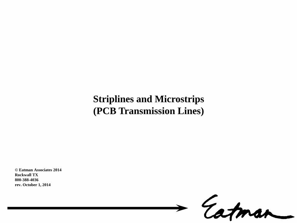
PC Board Traces as Transmission Lines:
• Board traces are conductors
• The board material itself (FR-4, etc.) is a dielectric
• Impedance discontinuities ► reflected waves
• At DC frequency (zero Hz), the return signal follows the
path of least resistance
• At RF frequencies, the return signal follows the path of least
impedance

Characteristic Impedance Z0:
• In the ideal case of a “lossless” transmission line
(line resistance and conductance = 0)
lossless line
1. Capacitance goes up, Z0 goes down
- higher εr and thinner dielectric = higher capacitance
2. Inductance goes up, Z0 goes up
- wider signal traces have lower inductance
Z0 = sqrt (L/C)
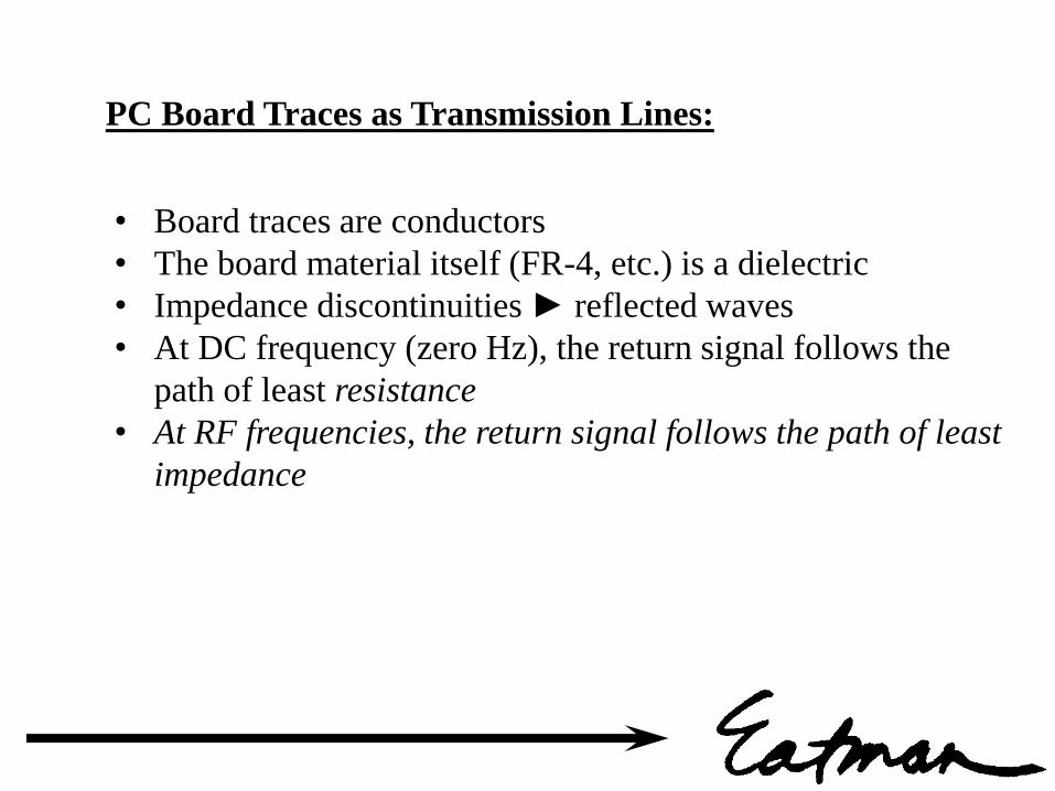
Typical PCB Trace Impedance Discontinuities:
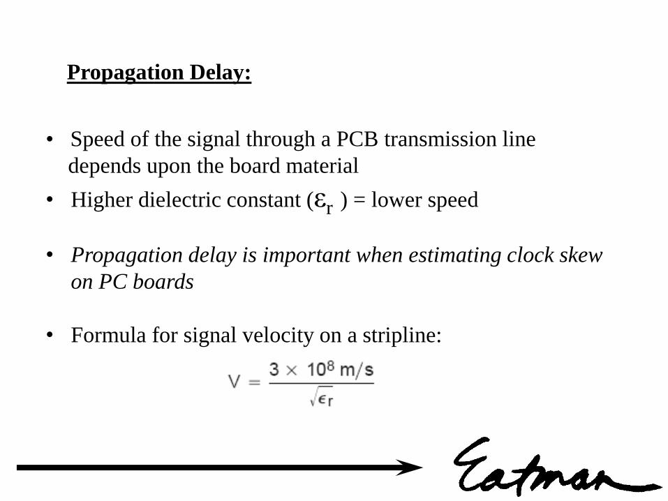
Propagation Delay:
• Speed of the signal through a PCB transmission line
depends upon the board material
• Higher dielectric constant (εr ) = lower speed
• Propagation delay is important when estimating clock skew
on PC boards
• Formula for signal velocity on a stripline:
Types of PC Board Transmission Lines
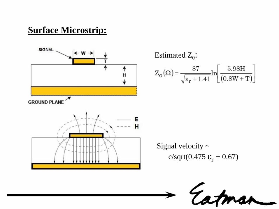
Surface Microstrip:
Estimated Z0:
Signal velocity ~
c/sqrt(0.475 εr + 0.67)
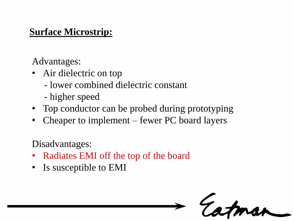
Surface Microstrip:
Advantages:
• Air dielectric on top
- lower combined dielectric constant
- higher speed
• Top conductor can be probed during prototyping
• Cheaper to implement – fewer PC board layers
Disadvantages:
• Radiates EMI off the top of the board
• Is susceptible to EMI
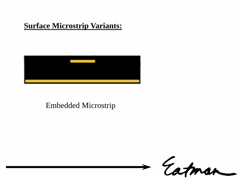
Surface Microstrip Variants:
Embedded Microstrip Embedded Microstrip
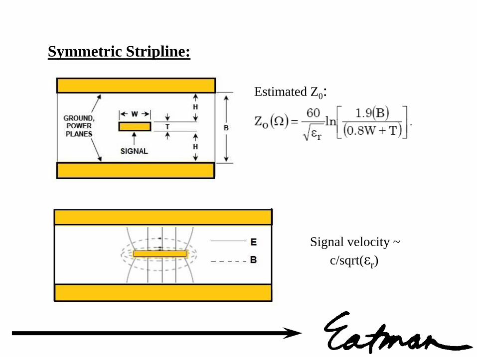
Symmetric Stripline:
Estimated Z0:
Signal velocity ~
c/sqrt(εr)

Stripline:
Advantages:
• Signal traces shielded – less EMI, less crosstalk
Disadvantages:
• Difficult to troubleshoot – no top board access
• More costly (more layers)
• For flex circuits, less flexible (thicker)
• Slower speed

Stripline variants:
Asymmetric Stripline Edge-coupled Stripline

Other Surface Topologies:
Coplanar Waveguide (CPW)
Edge-coupled CPW
with Ground (CPWG)
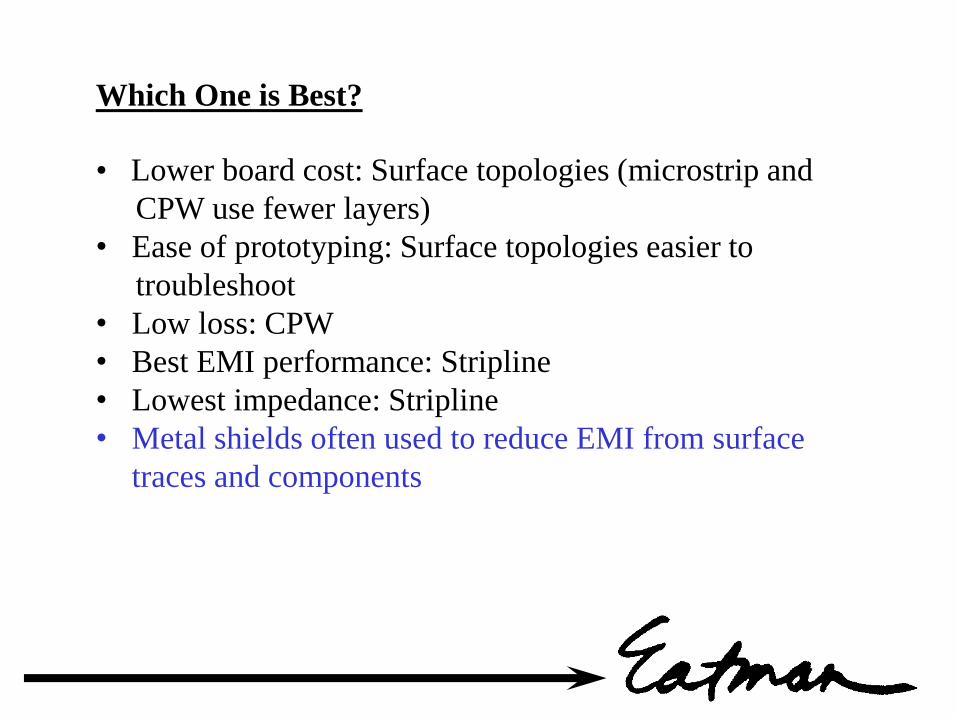
Which One is Best?
• Lower board cost: Surface topologies (microstrip and
CPW use fewer layers)
• Ease of prototyping: Surface topologies easier to
troubleshoot
• Low loss: CPW
• Best EMI performance: Stripline
• Lowest impedance: Stripline
• Metal shields often used to reduce EMI from surface
traces and components

Which One is Best?
• Adhesiveless flex circuit cores have better
thickness control
• Teflon® composite flex material can have εr as low as
2.3 and loss tangent of .0015
• Low Dk rigid board laminates are also available
- suitable for very high speeds
• Soldermasks have dielectric properties and loss
tangents similar to board materials
- affects performance of microstrip and CPW
Reducing Unwanted Coupling (Crosstalk)

Reducing Unwanted Coupling (Crosstalk):
• Crosstalk is caused by undesired capacitive, inductive, or
conductive coupling from one circuit, part of a circuit, or
channel, to another. Coupling affects impedance.
• A transmission line can be a EMI source and/or victim
• Reducing unwanted coupling requires reorientation, distance,
or shielding
• Effect of coupling decreases with the square of the distance
between the conductors
Minimizing Crosstalk:
• Use striplines or embedded microstrips vs microstrips
• Minimize congestion of traces through component placement
• Move signal lines as close to the ground plane as possible
- while maintaining the desired impedance
• Minimize parallel run lengths between signals
• Route signals on different layers orthogonal to each other

Minimizing Crosstalk:
• For single-ended line:
Keep adjacent traces as far apart as possible
- at least 2 trace widths
• For a differential pair: crosstalk cancels out
Route differential pair traces (for one signal) as close
together as possible
• Use differential pairs with equal length lines
Nested bends = unequal length traces

Transmission Line Losses

Components of Attenuation / Signal Loss:
• Metal (resistive) losses
- “skin effect” loss proportional to sqrt (frequency)
- also affected by metal surface roughness (“tooth”)
• Dielectric loss
- proportional to frequency – see “loss tangent”
• Dielectric conductivity loss
- stable over frequency
- may be ignored if resistivity > 10,000 Ohm-cm
• Radiation loss

Bad Design ► Bad Performance
• Choose the right PC board materials:
- choose material properties @ frequency of use
- choose metal for resistance @ frequency
• Use good general PC board layout practices:
- don’t route separate signals in parallel
- eliminate sharp corners on traces
- avoid ground plane slots
- use clean return paths directly under signal lines
- pick the right stackup
- etc…

PC Board Manufacturing Issues Affecting Impedance:
• Interlayer voids = ∆ capacitance
• Pre-preg thickness variation = ∆ capacitance
• Poor via-to-pad registration - drill deflection
• Inconsistent etching ► varying trace widths
• RA copper has less “tooth” than ED copper
• Vendor and processes affect your outcome

Transmission line design goals:
Perfect transfer of power (signal) from one end to the
other (source to load)
• No signal reflections down the line (no discontinuities)
• No radiated or induced EMI (no coupling or crosstalk)
• No amplitude reduction (no resistive or dielectric losses)
All this in a double sided board with a tight layout, dirt
cheap materials, and a sketchy board fabricator
NOT EXACTLY

The End