Embed Size (px)
Citation preview
Stress Estimation in Open Tungsten TSV
A. P. Singulani*†, H. Ceric*†, and S. Selberherr* *Institute for Microelectronics, TU Wien, Gußhausstraße 27–29/E360, A-1040 Wien, Austria
†Christian Doppler Laboratory for Reliability Issues in Microelectronics at Institute for Microelectronics, Wien, Austria
Email: {singulani|ceric|selberherr}@iue.tuwien.ac.at
Abstract—We have studied the residual stress formation in the metal film of a Through Silicon Via (TSV) technology. The film is deposited by a CVD process in the TSV’s wall and a residual stress arises due to this process. Our goal was to develop a methodology to estimate the stress based on growth parameters. The calculation results exhibit a good agreement with experiments, although there is a tendency for stress underestimation.
I. INTRODUCTION Three-dimensional (3D) integration in semiconductor
technology provides an alternative for keeping the current pace of miniaturization and enhances devices’ capabilities. The advantages can be summarized briefly as increased density, broader functionality, and higher performance per unit area, by making efficient use of the third dimension [1], [2]. However, three-dimensional integration opens up new challenges in design and fabrication, which must be overcome in order to achieve large scale production [1], [2].
The Through Silicon Via (TSV) is one of the main elements of 3D integration technology. TSVs enables vertical connections between dies such that devices can be piled-up, thereby increasing the integration density of the technology. However, the addition of large metal vias in the middle of a die creates mechanical reliability problems. Thermo-mechanical stress arises from the difference between the coefficient of thermal expansion (CTE) of silicon and the interconnection metal. At the same time intrinsic stress arises as a result of different physical mechanisms which take place during metal deposition. Those stresses, if not managed properly, can be driving forces to delamination and cracking mechanisms, which eventually lead to device failure.
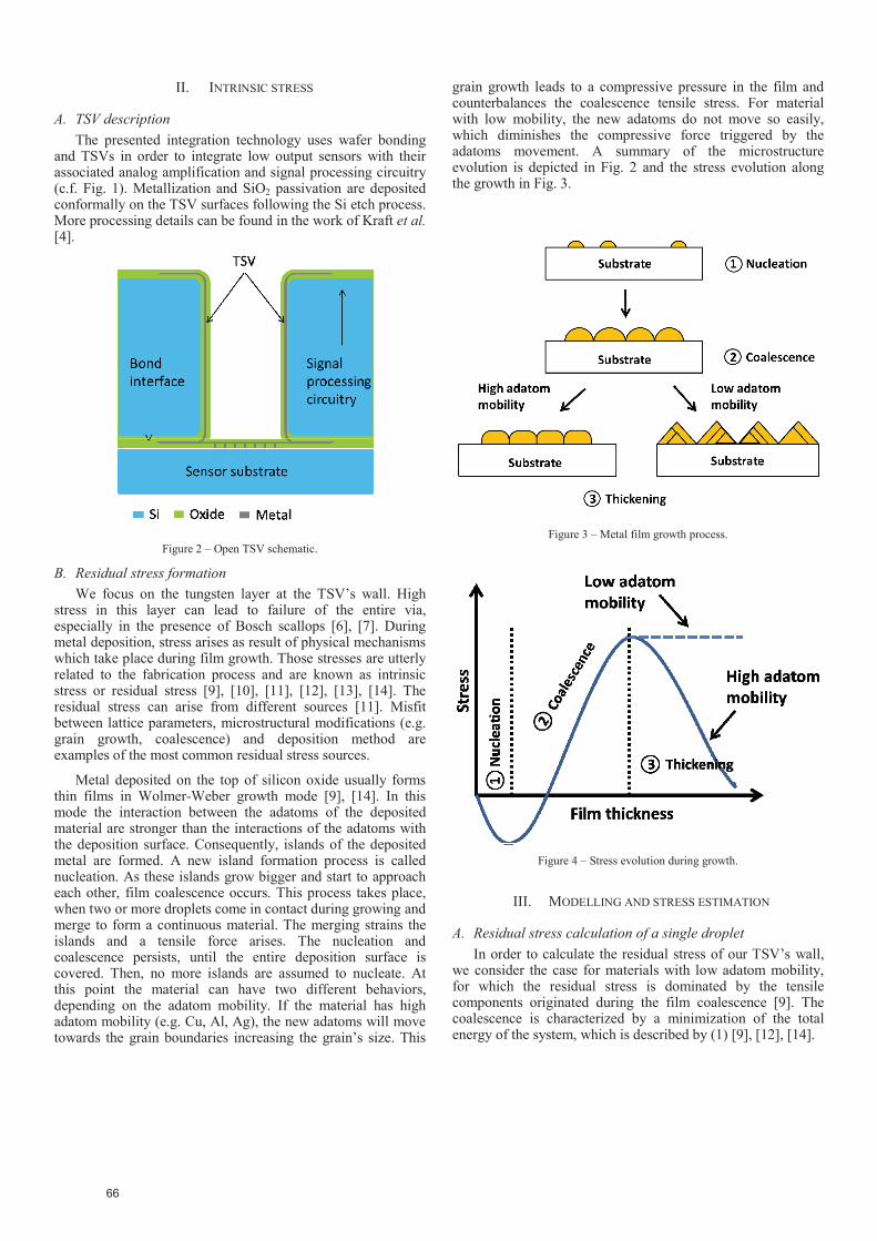
Several TSV designs were proposed as attempt to hinder the stress impact in the structure. The strategies usually involve a careful choice of the interconnection metal and via’s geometry with the purpose to reduce or to compensate the CTE mismatch. Cylindrically shaped TSVs are the most successful designs, since there are no sharp corners to induce stress accumulation. An additional stress reduction can be achieved by insertion of a polymer barrier between the via and the silicon [3]. The barrier absorbs the stress and prevents its propagation towards the silicon. A different approach is the utilization of open (unfilled) vias [4], [5]. Utilizing such TSVs reduces the amount of material in the structure and provides room for the metal to expand freely towards the axis of the via,
leading to an overall stress reduction. A summary of this discussion is sketched in Fig. 1.
Figure 1 – Three cylindrical TSV designs: (A) Filled TSV, (B) Filled TSV with liners, and (C) open (unfilled) TSV.
The choice of the interconnection metal is a critical step of the TSV’s design. The material should combine good electrical properties with low CTE mismatch to silicon. Copper is a common option due to the high conductivity of the material and the fabrication easiness. However, the difference of more than one order of magnitude between silicon and copper CTEs affects negatively the mechanical reliability. Tungsten is used as an alternative to copper, especially in TSVs for which the mechanical stress is a major concern. Although tungsten does not bear the electrical qualities of copper, the CTE mismatch to silicon is very low. But on the other hand, tungsten films usually exhibit a very high residual stress after the deposition process, which is a drawback especially for open TSVs.
The TSV technology considered in this work is an open via with tungsten as interconnection metal [4]. We have investigated mechanical aspects of this structure in several previous papers [5], [6], [7]. Other works have explored the electrical properties [2], processing [4], and experimental mechanical characterization [8] of this technology. In this paper we focus on the residual stress which arises in the metal layer of the TSV. Our goal is to provide a methodology to estimate the residual stress on the metal layer. In that way, the residual stress can be properly accounted during the device design.
978-1-4673-5736-4/13/$31.00 ©2013 IEEE 65
II. INTRINSIC STRESS
A. TSV description The presented integration technology uses wafer bonding
and TSVs in order to integrate low output sensors with their associated analog amplification and signal processing circuitry (c.f. Fig. 1). Metallization and SiO2 passivation are deposited conformally on the TSV surfaces following the Si etch process. More processing details can be found in the work of Kraft et al. [4].
Figure 2 – Open TSV schematic.
B. Residual stress formation We focus on the tungsten layer at the TSV’s wall. High
stress in this layer can lead to failure of the entire via, especially in the presence of Bosch scallops [6], [7]. During metal deposition, stress arises as result of physical mechanisms which take place during film growth. Those stresses are utterly related to the fabrication process and are known as intrinsic stress or residual stress [9], [10], [11], [12], [13], [14]. The residual stress can arise from different sources [11]. Misfit between lattice parameters, microstructural modifications (e.g. grain growth, coalescence) and deposition method are examples of the most common residual stress sources.
Metal deposited on the top of silicon oxide usually forms thin films in Wolmer-Weber growth mode [9], [14]. In this mode the interaction between the adatoms of the deposited material are stronger than the interactions of the adatoms with the deposition surface. Consequently, islands of the deposited metal are formed. A new island formation process is called nucleation. As these islands grow bigger and start to approach each other, film coalescence occurs. This process takes place, when two or more droplets come in contact during growing and merge to form a continuous material. The merging strains the islands and a tensile force arises. The nucleation and coalescence persists, until the entire deposition surface is covered. Then, no more islands are assumed to nucleate. At this point the material can have two different behaviors, depending on the adatom mobility. If the material has high adatom mobility (e.g. Cu, Al, Ag), the new adatoms will move towards the grain boundaries increasing the grain’s size. This
grain growth leads to a compressive pressure in the film and counterbalances the coalescence tensile stress. For material with low mobility, the new adatoms do not move so easily, which diminishes the compressive force triggered by the adatoms movement. A summary of the microstructure evolution is depicted in Fig. 2 and the stress evolution along the growth in Fig. 3.
Figure 3 – Metal film growth process.
Figure 4 – Stress evolution during growth.
III. MODELLING AND STRESS ESTIMATION
A. Residual stress calculation of a single droplet In order to calculate the residual stress of our TSV’s wall,
we consider the case for materials with low adatom mobility, for which the residual stress is dominated by the tensile components originated during the film coalescence [9]. The coalescence is characterized by a minimization of the total energy of the system, which is described by (1) [9], [12], [14].
66
020 )2)(21()41( zEyE gbsTotal γγ −−= (1)
Where ETotal is the total energy of the system, E is the Young modulus, s is the free surface energy of the droplet, gb is the grain boundary surface energy, and y0 and z0 are the dimensions depicted on Fig. 5.
Figure 5 – Structure considered for coalescence simulation. The droplets come in contact at height z0 and the surface is displaced at most by y0.The angle formed between the droplet and the deposition substrate is identified by [9].
In the coalescence process the free surface energy of the droplets is exchanged by elastic energy and, as a consequence, a tensile stress arises in the film. To calculate the average stress created by the coalescence, we carried out Finite Element Method (FEM) simulations as described in a previous work [14]. The structure of Fig. 2 is considered and a prescribed displacement in both droplets towards the center till the height z0 is imposed. A FEM simulation example of our setup is presented in Fig. 6.
Figure 6 – FEM simulation for a single encounter between two droplets.
B. Residual stress estimation for the entire film However, the stress in a single droplet does not characterize
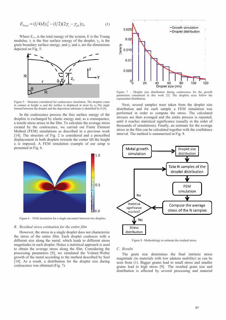
the stress of the entire film. Each droplet coalesces with a different size along the metal, which leads to different stress magnitudes in each droplet. Hence a statistical approach is used to obtain the average stress along the film. Considering the processing parameters [9], we simulated the Volmer-Weber growth of the metal according to the method described by Seel [14]. As a result, a distribution for the droplet size during coalescence was obtained (Fig. 7).
Figure 7 – Droplet size distribution during coalescence for the growth parameters considered in this work [3]. The droplets sizes follow the exponential distribution.
Next, several samples were taken from the droplet size distribution and for each sample a FEM simulation was performed in order to compute the stress. The calculated stresses are then averaged and the entire process is repeated, until it reaches statistical significance (usually in the order of thousands of simulations). Finally, an estimate for the average stress in the film can be calculated together with the confidence interval. The method is summarized in Fig. 8.
Figure 8 –Methodology to estimate the residual stress.
C. Results The grain size determines the final intrinsic stress
magnitude (in materials with low adatom mobility) as can be seen from (1). Bigger grains lead to small stress and smaller grains lead to high stress [9]. The resulted grain size and distribution is affected by several processing and material
67
parameters. However, a process engineer can control - to some extent - grain size distribution only by the growth rate and the nucleation rate. Thus, the intrinsic stress can be engineered, in principle, solely by those two rates. We neglect at this discussion any other processing step after deposition, which alters the microstructure of the material (e.g. annealing). Models which discuss those processes can be found in previous works.
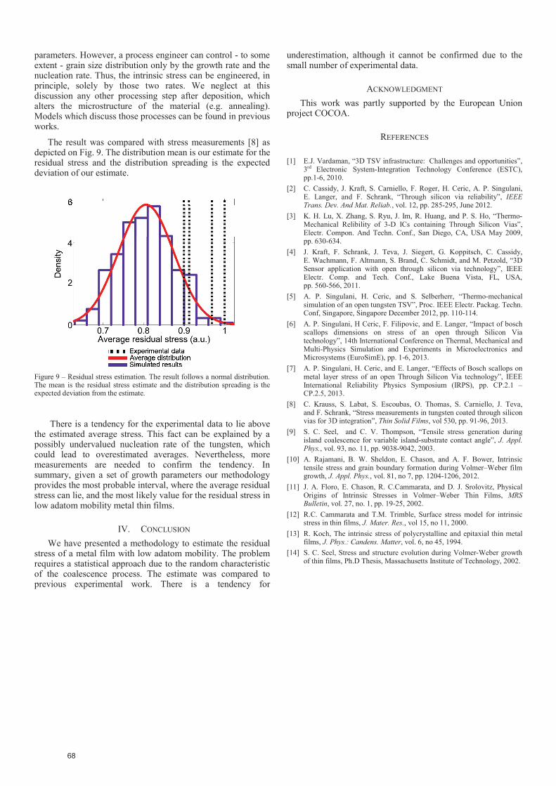
The result was compared with stress measurements [8] as depicted on Fig. 9. The distribution mean is our estimate for the residual stress and the distribution spreading is the expected deviation of our estimate.
Figure 9 – Residual stress estimation. The result follows a normal distribution. The mean is the residual stress estimate and the distribution spreading is the expected deviation from the estimate.
There is a tendency for the experimental data to lie above the estimated average stress. This fact can be explained by a possibly undervalued nucleation rate of the tungsten, which could lead to overestimated averages. Nevertheless, more measurements are needed to confirm the tendency. In summary, given a set of growth parameters our methodology provides the most probable interval, where the average residual stress can lie, and the most likely value for the residual stress in low adatom mobility metal thin films.
IV. CONCLUSION We have presented a methodology to estimate the residual
stress of a metal film with low adatom mobility. The problem requires a statistical approach due to the random characteristic of the coalescence process. The estimate was compared to previous experimental work. There is a tendency for
underestimation, although it cannot be confirmed due to the small number of experimental data.
ACKNOWLEDGMENT This work was partly supported by the European Union
project COCOA.
REFERENCES
[1] E.J. Vardaman, “3D TSV infrastructure: Challenges and opportunities”, 3rd Electronic System-Integration Technology Conference (ESTC), pp.1-6, 2010.
[2] C. Cassidy, J. Kraft, S. Carniello, F. Roger, H. Ceric, A. P. Singulani, E. Langer, and F. Schrank, “Through silicon via reliability”, IEEE Trans. Dev. And Mat. Reliab., vol. 12, pp. 285-295, June 2012.
[3] K. H. Lu, X. Zhang, S. Ryu, J. Im, R. Huang, and P. S. Ho, “Thermo-Mechanical Relibility of 3-D ICs containing Through Silicon Vias”, Electr. Compon. And Techn. Conf., San Diego, CA, USA May 2009, pp. 630-634.
[4] J. Kraft, F. Schrank, J. Teva, J. Siegert, G. Koppitsch, C. Cassidy, E. Wachmann, F. Altmann, S. Brand, C. Schmidt, and M. Petzold, “3D Sensor application with open through silicon via technology”, IEEE Electr. Comp. and Tech. Conf., Lake Buena Vista, FL, USA, pp. 560-566, 2011.
[5] A. P. Singulani, H. Ceric, and S. Selberherr, “Thermo-mechanical simulation of an open tungsten TSV”, Proc. IEEE Electr. Packag. Techn. Conf, Singapore, Singapore December 2012, pp. 110-114.
[6] A. P. Singulani, H Ceric, F. Filipovic, and E. Langer, “Impact of bosch scallops dimensions on stress of an open through Silicon Via technology”, 14th International Conference on Thermal, Mechanical and Multi-Physics Simulation and Experiments in Microelectronics and Microsystems (EuroSimE), pp. 1-6, 2013.
[7] A. P. Singulani, H. Ceric, and E. Langer, “Effects of Bosch scallops on metal layer stress of an open Through Silicon Via technology”, IEEE International Reliability Physics Symposium (IRPS), pp. CP.2.1 – CP.2.5, 2013.
[8] C. Krauss, S. Labat, S. Escoubas, O. Thomas, S. Carniello, J. Teva, and F. Schrank, “Stress measurements in tungsten coated through silicon vias for 3D integration”, Thin Solid Films, vol 530, pp. 91-96, 2013.
[9] S. C. Seel, and C. V. Thompson, “Tensile stress generation during island coalescence for variable island-substrate contact angle”, J. Appl. Phys., vol. 93, no. 11, pp. 9038-9042, 2003.
[10] A. Rajamani, B. W. Sheldon, E. Chason, and A. F. Bower, Intrinsic tensile stress and grain boundary formation during Volmer–Weber film growth, J. Appl. Phys., vol. 81, no 7, pp. 1204-1206, 2012.
[11] J. A. Floro, E. Chason, R. C.Cammarata, and D. J. Srolovitz, Physical Origins of Intrinsic Stresses in Volmer–Weber Thin Films, MRS Bulletin, vol. 27, no. 1, pp. 19-25, 2002.
[12] R.C. Cammarata and T.M. Trimble, Surface stress model for intrinsic stress in thin films, J. Mater. Res., vol 15, no 11, 2000.
[13] R. Koch, The intrinsic stress of polycrystalline and epitaxial thin metal films, J. Phys.: Candens. Matter, vol. 6, no 45, 1994.
[14] S. C. Seel, Stress and structure evolution during Volmer-Weber growth of thin films, Ph.D Thesis, Massachusetts Institute of Technology, 2002.
68