Embed Size (px)
Citation preview
1
Project Number: SJB MQP 2A11
Stray Voltage Detector
A Major Qualifying Project Report
Submitted to the Faculty
Of
WORCESTER POLYTECHNIC INSTITUTE
In partial fulfillment of the requirements for a
Bachelor of Science Degree
In
Electrical & Computer Engineering
By
____________________________________
Andrew Dawson
____________________________________
Michael Flaherty
____________________________________
Steven Tidwell
April 26, 2012
____________________________________
Professor Stephen J. Bitar, Major Advisor
____________________________________
Professor Alexander Emanuel, Co-Advisor

2
ACKNOWLEDGEMENTS
We would like thank Professor Stephen Bitar and Professor Alexander Emanuel for
advising us throughout the year on this project. Their knowledge and support helped us to
maintain our focus and lead to an overall successful MQP experience.
We would also like to thank Tom Angelotti and Pat Morrison from the Atwater Kent
ECE Shop. They helped us to find the appropriate components and materials needed in designing
our prototype.
Additionally, students Craig Janeczek and Greg Overton were instrumental in the
development of the LED output display circuitry and the mechanical aspects. We’d also like to
thank our family and friends for their continued support in our project endeavors.

3
ABSTRACT
The purpose of this project is to design and create a handheld device that can detect stray
voltage sources from a distance of a few meters away. The detector consists of a directional
antenna, an analog signal processing circuit powered by a 9V battery, and a grounded shield to
eliminate parasitic sources. The device is configured to detect electrified sources at 60Hz and
the signal strength is shown through an LED bar display driven by a digital A/D circuit.

4
EXECUTIVE SUMMARY
In our technologically driven society, we must be sure that what powers our homes and
our way of life is safely controlled. Unfortunately, life threatening incidences involving stray
voltage sources happen more often than they should. Though there are ways to detect these
electrified sources, they are limited in their use and most devices available require physical
contact with the object. With this project, we hoped to bridge the gap between the handheld
devices that require direct contact with the sources and the large, general location devices. Our
goal was to develop an easily portable, handheld device that can detect stray voltage sources of
120V, 60Hz, from a distance of a few meters.
As our project is a continuation of a previous stray voltage project, we wanted to address
the issues that remained unresolved. First, the previous year’s project wasn’t a handheld device.
Second, it didn’t solve the problem of the capacitive coupling effect between the device and its
surroundings. As our device is handheld, and thus has a “floating ground,” capacitive coupling
to various electrical noise sources has an effect on our ground reference point. To better
understand how we could resolve this issue, we decided to start at the beginning through a few
preliminary experiments.
For our first test, we connected a metal pole to an electrical socket to simulate a stray
voltage source of 120V and 60Hz. Using an aluminum plate connected to an oscilloscope to
detect the electrico magnetic field (EMF) signal given off by the pole at various distances, we
were able to get an estimate of what sort of signal we could detect before incorporating a
filtering and amplification circuit. To see if a different electrified object would give us similar
results, our next test involved connecting an aluminum plate of comparable size to our detection
plate to an electrical outlet. Connecting our detection plate to the oscilloscope, and taking
measurements at the same distances as in the previous test, we saw results that were consistent to
that of the charged pole experiment.
With results to compare to later on in the development of our device, we started to
develop a theoretical model for our circuit. While discussing what sort of problems we would
confront, we determined four distinct issues. First, we knew our device must read a voltage
signal by capacitively coupling to the source through the air. Next, as we wanted to optimize
distance sensitivity with relatively small antennas, it became apparent that the received signal
5
would have to be amplified. We also assumed that there might be more than one charged source
in the area we would be detecting, and would thus need some type of shielding for our antenna to
prevent those sources from affecting the signal we wanted to detect. Lastly, we knew the human
body had a capacitive and resistive value relative to the surface it was standing on. This would
have to be accounted for in our design. With these issues in mind, we proceeded to create the
following model.
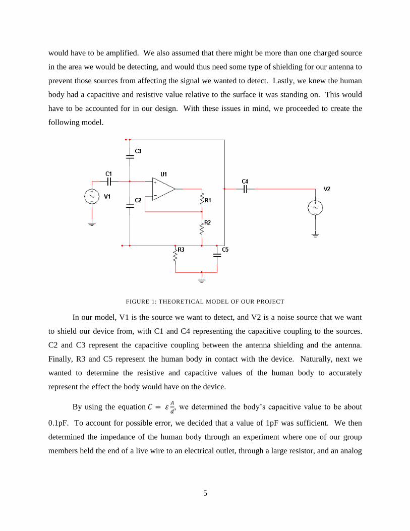
FIGURE 1: THEORETICAL MODEL OF OUR PROJECT
In our model, V1 is the source we want to detect, and V2 is a noise source that we want
to shield our device from, with C1 and C4 representing the capacitive coupling to the sources.
C2 and C3 represent the capacitive coupling between the antenna shielding and the antenna.
Finally, R3 and C5 represent the human body in contact with the device. Naturally, next we
wanted to determine the resistive and capacitive values of the human body to accurately
represent the effect the body would have on the device.
By using the equation
, we determined the body’s capacitive value to be about
0.1pF. To account for possible error, we decided that a value of 1pF was sufficient. We then
determined the impedance of the human body through an experiment where one of our group
members held the end of a live wire to an electrical outlet, through a large resistor, and an analog
6
voltmeter. The calculated impedance value came to be 10MΩ. With these values, we could then
begin to design and assemble our detector.
Our device uses a fairly simple amplification circuit with a bandwidth filter to make sure
that we only detect 60Hz signals. It is also designed to run on a common, 9V battery. Similar in
appearance to a radar gun, our detector is a directionally sensitive device. The handle, which
houses the battery, is attached to an electrical conduit pipe used to shield the antenna and
detection circuit.
With our final prototype assembled, we conducted a distance and viewing angle
performance tests to determine the optimal antenna depth within the shielding. From our tests,
our device was able to detect a stay voltage source from over 3 meters away, exceeding our
initial expectations.

7
TABLE OF CONTENTS
Acknowledgements ......................................................................................................................... 2
Abstract ........................................................................................................................................... 3
Executive Summary ........................................................................................................................ 4
Table of Figures ............................................................................................................................ 10
Table of Tables ............................................................................................................................. 12
Introduction ................................................................................................................................... 13
Problem Statement .................................................................................................................... 13
Background ................................................................................................................................... 15
Literature Review...................................................................................................................... 15
Article One ............................................................................................................................ 15
Article Two ........................................................................................................................... 16
Article Three ......................................................................................................................... 16
Case Studies .............................................................................................................................. 17
Case One ............................................................................................................................... 17
Case Two .............................................................................................................................. 17
Case Three ............................................................................................................................ 18
Consolidate Edison ............................................................................................................... 18
Prior Art .................................................................................................................................... 19
Patent One ............................................................................................................................. 19
Patent Two ............................................................................................................................ 21
Patent Three .......................................................................................................................... 22
Initial Design Considerations ........................................................................................................ 23
Floating Ground, Capacitive Coupling & Body Impedance ..................................................... 23

8
Determining Coupling Capacitance ...................................................................................... 23
Charged Pole Experiment ......................................................................................................... 24
Charged Pole Experiment Results ........................................................................................ 26
Parallel Plate Experiment .......................................................................................................... 28
The Human Impedance Test ..................................................................................................... 32
Human Impedence Test Findings ......................................................................................... 34
Developing a Circuit ................................................................................................................. 34
Deriving the Equation from our Model .................................................................................... 36
Inverting vs. Non-inverting Configurations .............................................................................. 40
JFET vs. CMOS AMplifier ....................................................................................................... 42
Schematic .................................................................................................................................. 42
Biasing the Input Pins ............................................................................................................... 43
Zeroing the Offset ..................................................................................................................... 44
Filtering ..................................................................................................................................... 44
Assembly of the Detector .......................................................................................................... 45
Methodology ................................................................................................................................. 46
Antenna ..................................................................................................................................... 46
Shielding ................................................................................................................................... 47
Gain Stage ................................................................................................................................. 48
60 Hz Bandpass Filter ............................................................................................................... 48
Creating a Printed Circuit Board............................................................................................... 49
MSP430 Input ........................................................................................................................... 50
LED Output ............................................................................................................................... 52
Results ........................................................................................................................................... 53

9
Filter Test .............................................................................................................................. 54
Amplifier Test ....................................................................................................................... 55
Antenna Depth and Performance Tests ..................................................................................... 57
Viewing Angle Experiment .................................................................................................. 57
Distance Test ......................................................................................................................... 60
Recommendations ......................................................................................................................... 62
Conclusion .................................................................................................................................... 62
Final Device Design ...................................................................................................................... 64
Appendix ....................................................................................................................................... 65
Code for Analog to Digital Converter (MSP430) ..................................................................... 65
References ..................................................................................................................................... 68

10
TABLE OF FIGURES
Figure 1: Theoretical Model of our Project .................................................................................... 5
Figure 2: Stray Voltage Detector .................................................................................................. 20
Figure 3: Hand-held Non-contact Voltage Tester ......................................................................... 21
Figure 4: High Voltage Switching Circuit .................................................................................... 22
Figure 5: First Test Configuration ................................................................................................ 24
Figure 6: Charged Pole's Voltage Waveform ............................................................................... 25
Figure 7: Second Test Configuration ............................................................................................ 25
Figure 8: Detected Voltage from 1” from Charged Pole .............................................................. 26
Figure 9: Detected Voltage from 4" from Charged Pole .............................................................. 26
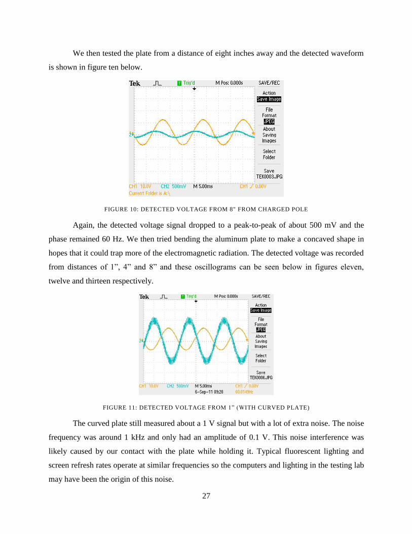
Figure 10: Detected Voltage from 8" from Charged Pole ............................................................ 27
Figure 11: Detected Voltage from 1” (with Curved Plate) ........................................................... 27
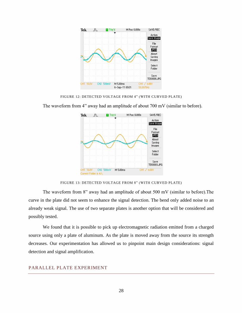
Figure 12: Detected Voltage from 4” (with Curved Plate) ........................................................... 28
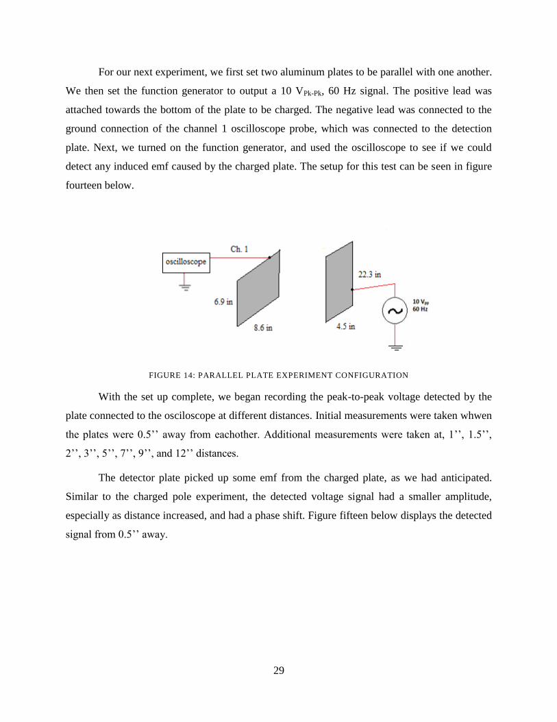
Figure 13: Detected Voltage from 8” (with Curved Plate) ........................................................... 28
Figure 14: Parallel Plate Experiment Configuration ..................................................................... 29
Figure 15: Detected Voltage from 0.5’’ ........................................................................................ 30
Figure 16: Detected Voltage from 1.5" ......................................................................................... 30
Figure 17: Detected Voltage from 3’’ with Phase Shift ............................................................... 30
Figure 18: Detected Voltage from 12’’ ......................................................................................... 31
Figure 19: Equivalent Resistance of Footwear ............................................................................. 34
Figure 20: Theoretical model of the project ................................................................................. 35
Figure 21: Basic Model of System................................................................................................ 36
Figure 22: System with Parasitic Source Disconnected ............................................................... 37
Figure 23: Norton Equivalent of System ...................................................................................... 38

11
Figure 24: Final System Representation ....................................................................................... 38
Figure 25:Value of voltage without parasitic influence ................................................................ 39
Figure 26: Simplified inverting configuration of our system ....................................................... 41
Figure 27: Simplified non-inverting configuration of our system ................................................ 41
Figure 28: Full schematic of our working system ........................................................................ 43
Figure 29: Block Diagram of Final Prototype .............................................................................. 46
Figure 30: Antenna used in Device Design .................................................................................. 47
Figure 31: Antenna's Location Inside the Shielding Tube ............................................................ 48
Figure 32: Inside of Shielding Tube ............................................................................................. 48
Figure 33: Ultiboard Circuit Image ............................................................................................... 50
Figure 34: Completed Printed Circuit Board ................................................................................ 50
Figure 35: LED Bar graph ............................................................................................................ 52
Figure 36: "waterfall" circuit ........................................................................................................ 53
Figure 37: Frequency set to 15 Hz ................................................................................................ 54
Figure 38: Frequency set to 60 Hz ................................................................................................ 54
Figure 39: Frequency set to 100 Hz .............................................................................................. 55
Figure 40: Frequency set to 1 kHz ................................................................................................ 55
Figure 41: Amplitude from d=1ft ................................................................................................. 56
Figure 42: Amplitude from d=2ft ................................................................................................. 56
Figure 43: Amplitude from d=3ft ................................................................................................. 56
Figure 44: Amplitude from d=4ft ................................................................................................. 57
Figure 45: Angle Experiment Setup ............................................................................................. 58
Figure 46: Antenna Depth Tradeoff .............................................................................................. 58
Figure 47: Recorded Volatge vs. Viewing Angle ......................................................................... 59

12
Figure 48: Distance Test Setup ..................................................................................................... 60
Figure 49: Recorded Voltage VS. Distance from Source ............................................................. 61
Figure 50: Profile of Stray Voltage Detector ................................................................................ 64
Figure 51: Front View of Stray Voltage Detector ........................................................................ 64
TABLE OF TABLES
Table 1: Measurements Taken at Each Distance .......................................................................... 31
Table 2: Angle Test Results .......................................................................................................... 59
Table 3: Distance Test Results ...................................................................................................... 61

13
INTRODUCTION
Electricity is a resource that many can’t imagine life without. It powers our home
appliances, cell phones, computers, and soon, it will even fuel our cars. Though electricity is
important in our daily lives, it is always important to remember that it can also present a hazard.
Some of these dangers occur as a result of faulty wiring or improper grounding. When an object
such as a street lamp or a manhole cover becomes electrically charged as a result, it becomes a
stray voltage source. Stray voltage sources have the potential to deliver a strong, sometimes
lethal shock to humans or animals that come into contact with them. Therefore, it is important to
be able to detect stray voltage sources before it has the chance to cause harm.
The goal of our project, which is a continuation of a previous stray voltage detection
project, is to create a handheld, easily portable device that can detect stray voltage sources of
120V, 60Hz, from a distance of a few meters. It will also attempt to solve the issues that were
not addressed in the previous project, such as the capacitive coupling effect between the device
and its surroundings. To accomplish this, we will be conducting tests to determine factors such
as the optimal antenna depth in the device to get the most sensitivity out of the device, and the
approximate signal strength we can expect at different distances before the amplification of the
detected signal.
PROBLEM STATEMENT
There are few devices currently available to detect stray voltage sources, and mostly
involve getting close enough to a potential source to physically touch it verify if the object is
electrically charged, such as voltage sniffers. Though there are devices available to detect these
sources at a distance, they must be attached to the back of a car due to their size, and they cannot
give you the specific location of a source, only a general area. From there, the person looking
for the stray voltage source must check each potentially electrified object with the devices that
require physical contact. Of course, the lack of detection range in these devices is a major
limitation, as finding the stray voltage source can sometimes turn into trying to find a needle in a
haystack.
Our project looks to bridge the gap between the handheld devices that require direct
contact with the sources and the large, general location devices. Our device will be able to be

14
easily carried around, and provide a reasonable detection radius, making the search for the
improperly charged objects quicker.

15
BACKGROUND
LITERATURE REVIEW
From previous research, it is apparent the term “stray voltage” is still ambiguous in the
professional community. From the article The Confusion Surrounding ‘Stray Voltage’ [1],
written by Jim Burke, we can see there are distinct attempts to eliminate this confusion.
By examining other articles relevant to stray voltage, we will be able to see in certain
instances when stray voltage has been detected. Since our project is based on stray voltage, we
must investigate cases in which stray voltage has caused harm to communities. The following
articles will be able to define and present stray voltage as harmful to a community.
ARTICLE ONE
The Confusion Surrounding ‘Stray Voltage’ By Jim Burke
The purpose of this article is to eliminate the confusion of the term “stray voltage” and
how it is used today. Burke proposes that the following terms will be useful in deciphering a
clear definition to stray voltage.
Neutral to earth voltage- the voltage on a neutral conductor as a result of
unbalanced loading.
Temporary Overvoltages- The high voltage caused temporarily by overcurrent
protection.
Contact voltage- where a live conductor makes contact with an exposed housing
or other conductive surfaces.
Step and Touch voltages – the voltage that can result across the body between the
feet or hands due to currents passing nearby.
Static Discharge- charge distribution caused by friction
High Impedance faults- a difficult fault to protect against because currents are
usually too low for overcurrent mechanisms.
Stray Current- currents traveling through the earth.
In his article, Burke argues the term “stray voltage” should only be used to refer to
neutral to earth voltage. Burke insists neutral to earth voltage is usually only quantized by
a few volts and rarely considered dangerous. He offers the explanation that industry
16
participation has decreased in the standards of writing and “has created a situation where
non-professionals, such as state legislators and lawyers are rewriting definitions, creating
new terms and creating arbitrary limits and testing procedures”. He also offers that these
non-professional parties have been “costing the industry many millions of dollars which
could have been used far more wisely to promote both safety and reliability.”
ARTICLE TWO
Diagnosis and Trouble Shooting of Stray Voltage Problems by Alvin Bierbaum
This article was written as an IEEE conference paper to justify The National Electric
Code (NEC). By using historical examples such as agriculture development, Bierbaum shows
how stray voltage has been an ongoing issue [2]. His primary case of question revolves around
the three phase power systems in dairy farms. In such systems, the NEC requires the neutral
conductor be tied to the neutral bus bar. Bierbaum explains, “The neutral bus bar must be bonded
to the panel box, ground rod and another grounding source that makes contact with a metallic
surface that has sufficient contact with the earth.” Relating this quote to the previous article, this
type code requirement would be categorized as contact voltages. The grounding of the bus bar
sets all the contacting metallic surfaces to ground. Bierbaum explains this code is instituted to
easily resolve grounding faults. He explains these faults can easily be solved by fusing or
breakers. Bierbaum also states his experience shows “at least 80 percent of the stray voltage
problems occur on the farmer’s side of the meter.”
ARTICLE THREE
Was Stray Voltage really stray? By Charlie Williams
This article was written in regards to residential communities complaining of high
voltage from a shower faucet [3]. The resident reported that while taking a shower and adjusting
the shower head, he would feel an electric shock. Curious, he measured the voltage relevant to
ground and experienced 26 Volts. Williams points out that stray voltage is more prevalent
around water because of its high conductivity. Eventually investigations discovered the
energized neutral source was accredited to an improperly wired street lamp. The street lamp in
question created a short in the circuit approximately one mile from his abode. Williams
17
continues to pose the question, “Is stray voltage really stray?” In this case, since the neutral was
connected directly to a transformer, it’s most likely not accredited to a stray effect.
CASE STUDIES
From the previous articles, we can see that stray voltage has been a concern in everyday
life. Stray voltage incidents have been reported more frequently in urban areas where urban
objects have been charged and have harmed people and animals alike either by shocking,
electrocuting and in worst cases, death. The following section discusses certain incidents that
could have been prevented with the use of a stray voltage detector.
More commonly, stray voltage incidents occur in urban areas. Due to the vast amount of
metallic surfaces and amount of electrically powered objects, the chances for faults are greater.
The more common surfaces which cause issues for the public tend to be street lamps, manhole
covers, and anything with public running water such as water fountains.
CASE ONE
The earliest and one of the more severe cases of stray voltage induced injury occurred in
March of 1994 [4]. While delivering a load of logs using a Cascade, a type of trailer loader, one
man was severely injured. The man was shocked when standing in a puddle of water while trying
to use the Cascade. He had pressed his stomach against the truck and reached over the truck’s
loader hook to operate the machine using the control box. As soon as he pressed the button, he
received an instantaneous shock and was knocked unconscious. The man suffered from multiple
internal electrical burns, but survived the ordeal.
CASE TWO
In 2004 in New York, a woman was walking her dogs down the street in East Village
when she was electrocuted [5]. The shock occurred when she walked over the metallic cover of
a utility box. After the incident, the woman sued Consolidate Edison, the electric company that
owned the utility box. After a cash settlement of $10.6 million, the Consolidate Edison Company
inspected the box and discovered that this incident was caused by improperly wrapped and
18
exposed wires within the box. As a result, the Consolidate Edison Company decided to begin
slowly examining the roads looking for potentially dangerous charged objects.
CASE THREE
A more recent case occurred in December 2009 in Santa Fe, New Mexico. While walking
their dogs, two women noticed one dog had jumped. They began to search for what had shocked
the dog [6] and soon after, the other dog fell to the ground in pain. Concerned, the women
returned the dogs to their cars and while walking by a lamp post, one speculated there could be a
short circuit within the post. While standing on wet concrete, she pressed her hand against the
pole and did feel a slight shock.
CONSOLIDATE EDISON
All of these occurrences ended in a lawsuit due to hazardous voltage levels that were
“invisible” until an electric shock occurred. If these cities had used devices such as stray voltage
detectors, these occurrences could have been avoided. Even companies that have taken large
hits, such as Consolidate Edison, could have used stray voltage detectors during routine
maintenance to determine where there may have been a hazard.
Due to the large number of reported incidents, Consolidate Edison spent around $10
million on stray voltage detectors and other precautionary devices to prevent further occurrences
of electrical harm [7]. One precautionary measure that they have been conducting annually is to
take surveys of “the underground system plus additional surveys within five days of storms that
result in the salting of city roadways.”
When the surveys were conducted, Consolidate Edison tested 728,789 pieces of
equipment from December 2004 to November 2005. Of these tested objects, a total of 1,214
objects were found to be sources of stray voltage. This number includes “1,083 streetlights, 99
utility poles, and 32 power-distribution structures like manholes, service boxes, and transformer
vaults” [8].
Consolidate Edison invested $100 million on stray voltage solutions. Part of the
investment included 15 mobile stray voltage detectors and 4 different kinds of handheld devices.
The mobile devices are rather large and will roam the streets year round on the back of pick-up

19
trucks. These devices will scan metallic objects remotely and can sense a level as small as 1 volt.
When the truck has sensed a voltage in a specific direction, the workmen would take to the
direction and test each metallic object (manhole covers, gratings, service boxes etc.) in the
vicinity the voltage was sensed.
According to the “City Room Blog” of the New York Times, the number of incidents has
decreased to about 24 incidents a month. While the number of incidents decreases, the number of
objects sense has increased to roughly 900 objects sensed per month. Nearly seventy-five percent
of these 900 objects are street lights, traffic lights, sidewalks, manhole covers, and fences.
Electrical shock has been an ever growing problem of the past few decades in urban
areas. However, Consolidate Edison has taken several motions to make positive strides in the
right direction. The above facts and figures concerning Consolidate Edison prove with the proper
equipment, these incidents can be avoided. Regardless of the number of increasing electrically
charged objects, we can still prevent severe incidents due to early detection.
PRIOR ART
In the field of stray voltage preventions there are several items of prior art that aid in
detecting electrically charged objects. We will examine several patents and devices that achieve
the same basic end result, but function differently than our own device.
PATENT ONE
The first patent we came across was patent number US 7,449,892 B2, a device used to
sense stray voltage through a portable housing that includes electrostatic charge sensors and field
intensity indicators [9]. The device is shown below:
20
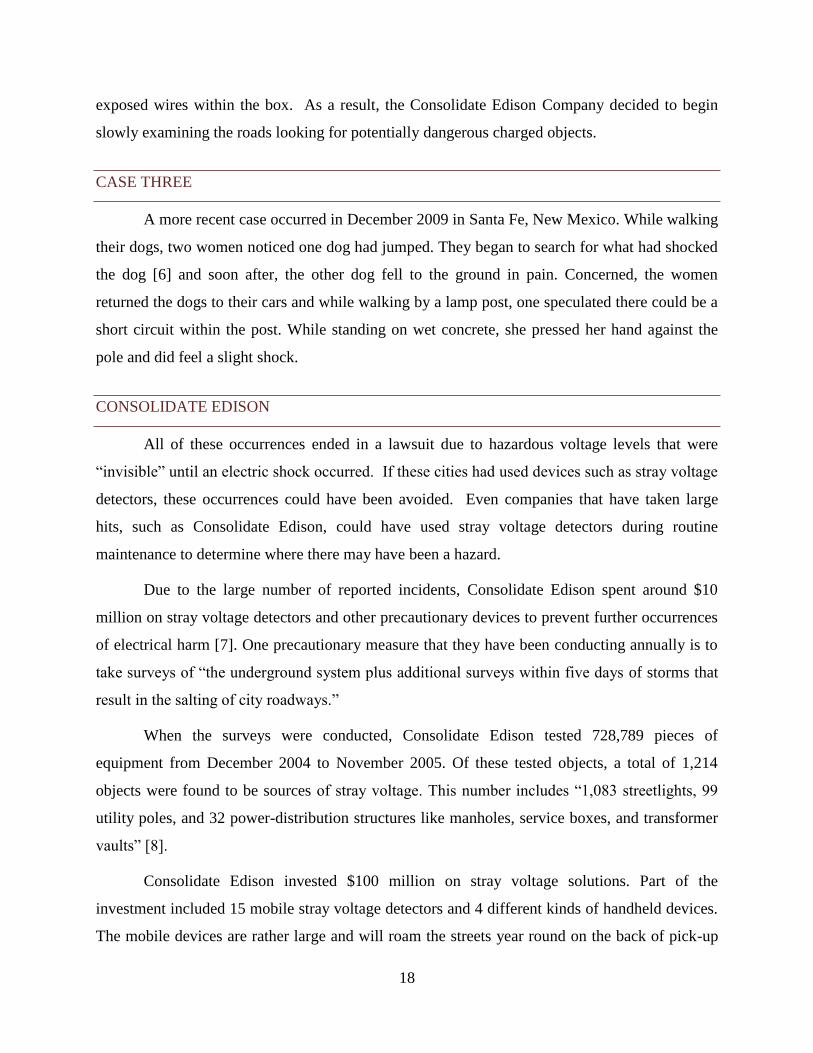
FIGURE 2: STRAY VOLTAGE DETECTOR
Invented by Daniel C. Wiswell, Meredith P. Peterson, and Jianping Sun, this device can
sense stray voltage through a capacitance between an electrically charged object and two
electrostatic plates along the same axis and two field intensity indicators which are connected
one of the charge sensors. Through the schematic, we observed that the signal was first
processed through a fixed gain stage which is then passed on through an adjustable gain stage
that is used to nullify parasitic noise. The overall gain of the system can be set from 1 to 10,000.
From here, the signal is processed through audio and visual indication blocks that utilize LEDs
and Headphones for the user interface. The patent mentions the LED indications can be carried
out through light intensity or by illuminating multiple LEDs in bar graph form to show field
intensity. The patent also claims that in some configurations, the left and right audio can be
output to show direction through a headset wearable by the user.
The patent mentions the “electrostatic charge sensors each comprise a plate of conductive
material on a circuit board.” It claims the plate is etched to reveal a copper layer of the board that
connects to components on the board using vias.
Patent No.: US 7,449,892 B2
Patent Date: November 11, 2008
21
When giving the full capabilities of the device, the patent claims the devices can be
mounted to robots, cars, and other vehicles that can roam the streets and sense voltage. This
would work well for urban cities and would save money in terms of salaries to pay people to do
the same automated work. However, the patent does not mention what the dynamic range the
device can sense. This could be accredited to the various cases in which the device can be
configured.
PATENT TWO
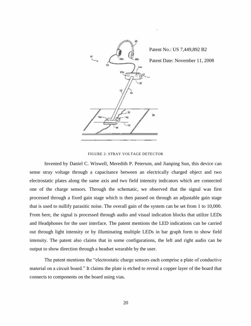
The second patent investigated is the hand-held non-contact voltage test [10]. We were
able to obtain a probe for under twenty dollars at The Home Depot®. The device is designed to
sense AC voltage through a small plate utilized as the receiving antenna. The generic
resemblance of the patent is shown below:
Figure 3: Hand-held Non-contact Voltage Tester
This device uses LED indicators and audio indicators to alert the user when a voltage is
detected. The probe can prevent false readings due to static build up on the antenna and only
allows signals of high enough frequency to initialize the device. The probe also has variable gain
options increasing or decreasing the minimum distance to sense a voltage. The downside to this
design, we noticed, was the range the probe could sense AC signals was limited. The device
Patent No.: US 6,828,767 B2
Patent Date: Dec. 7, 2004
22
would turn on at a maximum distance of a few inches from the source. In practice, this device is
only used to show live wires.
In our predicament, this probe would not be useful considering it does not have a low
pass filter which would eliminate any greater frequency signals. Our design is optimized to
operate at 50-60 Hz to sense voltages in urban areas. Anything above that threshold would be
considered noise or parasitic sources.
PATENT THREE
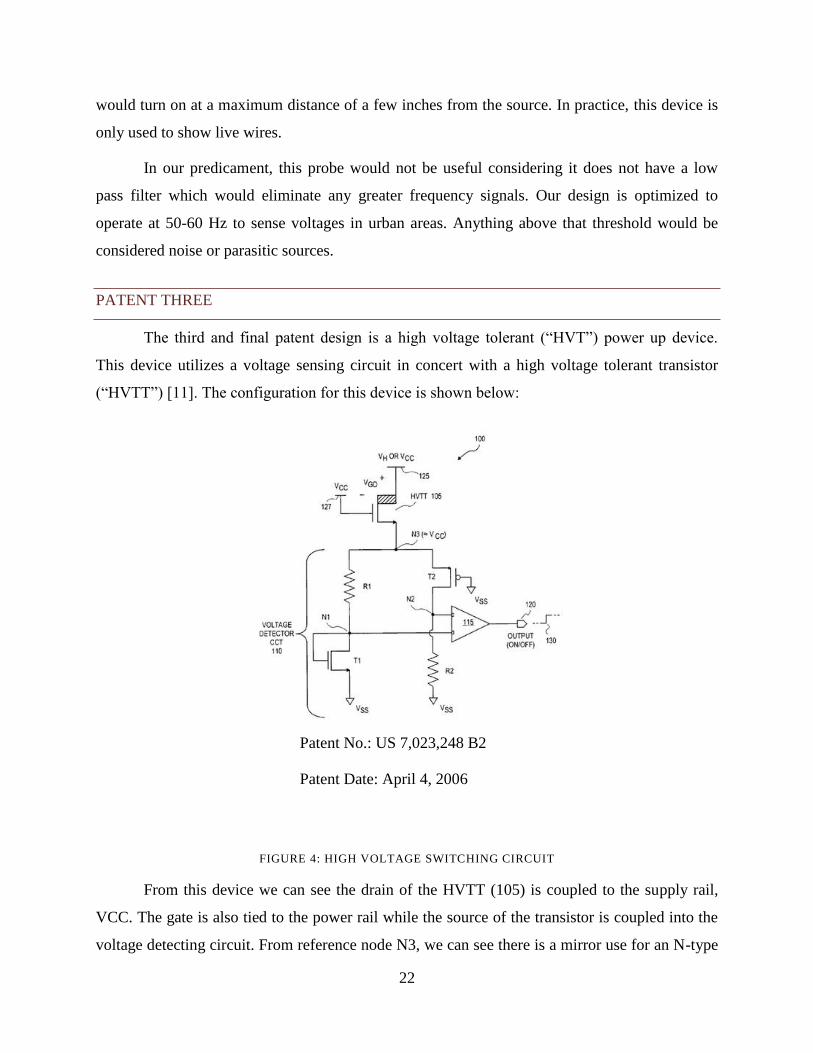
The third and final patent design is a high voltage tolerant (“HVT”) power up device.
This device utilizes a voltage sensing circuit in concert with a high voltage tolerant transistor
(“HVTT”) [11]. The configuration for this device is shown below:
FIGURE 4: HIGH VOLTAGE SWITCHING CIRCUIT
From this device we can see the drain of the HVTT (105) is coupled to the supply rail,
VCC. The gate is also tied to the power rail while the source of the transistor is coupled into the
voltage detecting circuit. From reference node N3, we can see there is a mirror use for an N-type
Patent No.: US 7,023,248 B2
Patent Date: April 4, 2006
23
MOSFET (“NMOS”) and a P-type MOSFET (“PMOS”). The NMOS has shorted the gate and
drain of the transistor and with R1 create a current path from N3 to ground. On the other end, the
concert of R2 and T2 also create another current path to ground. From these two parallel current
paths, a comparator is place between nodes N1 and N2 (115). This comparator will then compare
the values of N1 and N2 and output through the integrated circuit
In order for the output to be turned on to logic high, N3 would have to be greater or equal
to the supply voltage of the HVTT (105). This shows the transistor will not turn on unless the
voltage supply to the gate of 105 will not turn on unless it is above the threshold voltage.
INITIAL DESIGN CONSIDERATIONS
FLOATING GROUND, CAPACITIVE COUPLING & BODY IMPEDANCE
One large problem that our group encountered while designing this handheld device was
the effect of our “floating ground”. Our circuit uses a ground that’s not tied to the actual earth
ground (therefore “floating”); we can think of it as more of a reference potential. By “grounding”
our shield we hoped to provide a path for the noise to flow through. The challenge with handheld
devices is that electronic signals tend to capacitively couple with other sources (including
ground). This effect kept changing the potential at our reference ground as the distance to ground
was varied. Additionally, our body’s resistance through the hand to the ground will affect that
voltage potential. We performed a few experiments to see the effect that these happenings had on
our circuit’s accuracy.
DETERMINING COUPLING CAPACITANCE
To understand the effects that the coupling to ground will exhibit on our circuit, we
needed to estimate how large a capacitance is present. Using the equation for capacitance (shown
below) at a distance of one meter and an approximate shield area of 0.05 m2, we estimated the
capacitance to be on the order of 0.1 pF.
(1)
24
This device will need to operate outdoors which can increase the coupling capacitance to
ground. In order to account for this ‘error’ in our simulation, we estimated the ground-to-device
capacitance value at 1 pF.
CHARGED POLE EXPERIMENT
We first set the function generator to output a 10 VP-P, 60 Hz signal. The positive lead
was attached at the top of the metal pole (to simulate a charged light post). We then used a sheet
of coated aluminum attached to the oscilloscope to see if we could detect any induced EMF that
would’ve been caused by the magnetic flux from the post. The aluminum sheet was 16.7 cm in
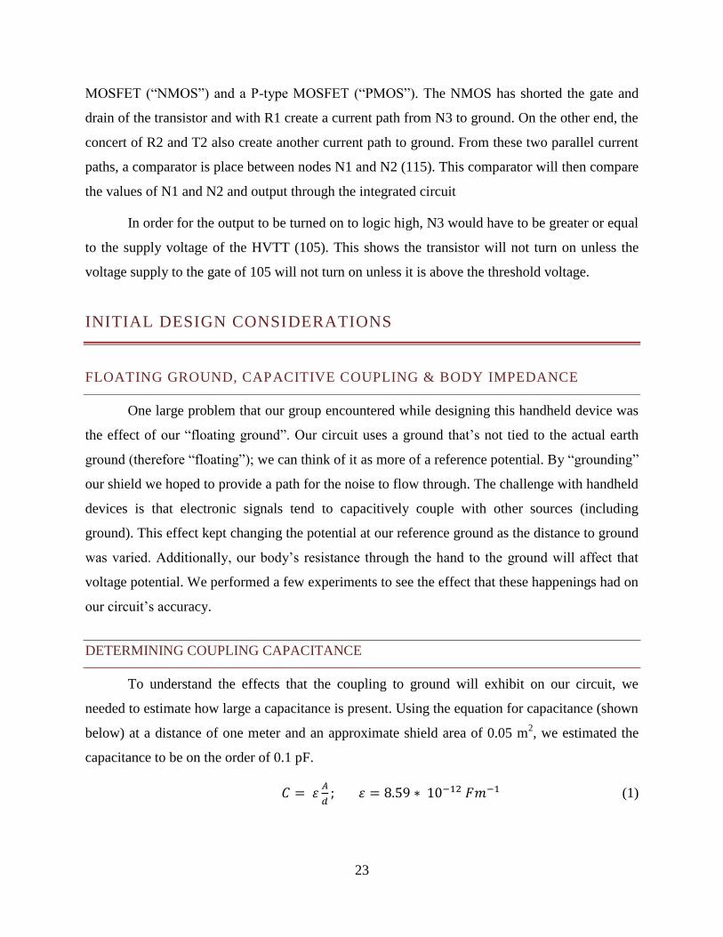
width, and 6.05 cm in length. For the first trial, the plate’s distance from the charged pole, d,
was approximately 1”. The charged pole stands at a height of 38.1 cm, shown as variable h, and
has a diameter, denoted by variable r, of 3.2 cm. The distance between the two objects was
increased in the next two trials to 4” and finally to 8” away. The setup for this first test can be
seen in figure five below.
FIGURE 5: FIRST TEST CONFIGURATION
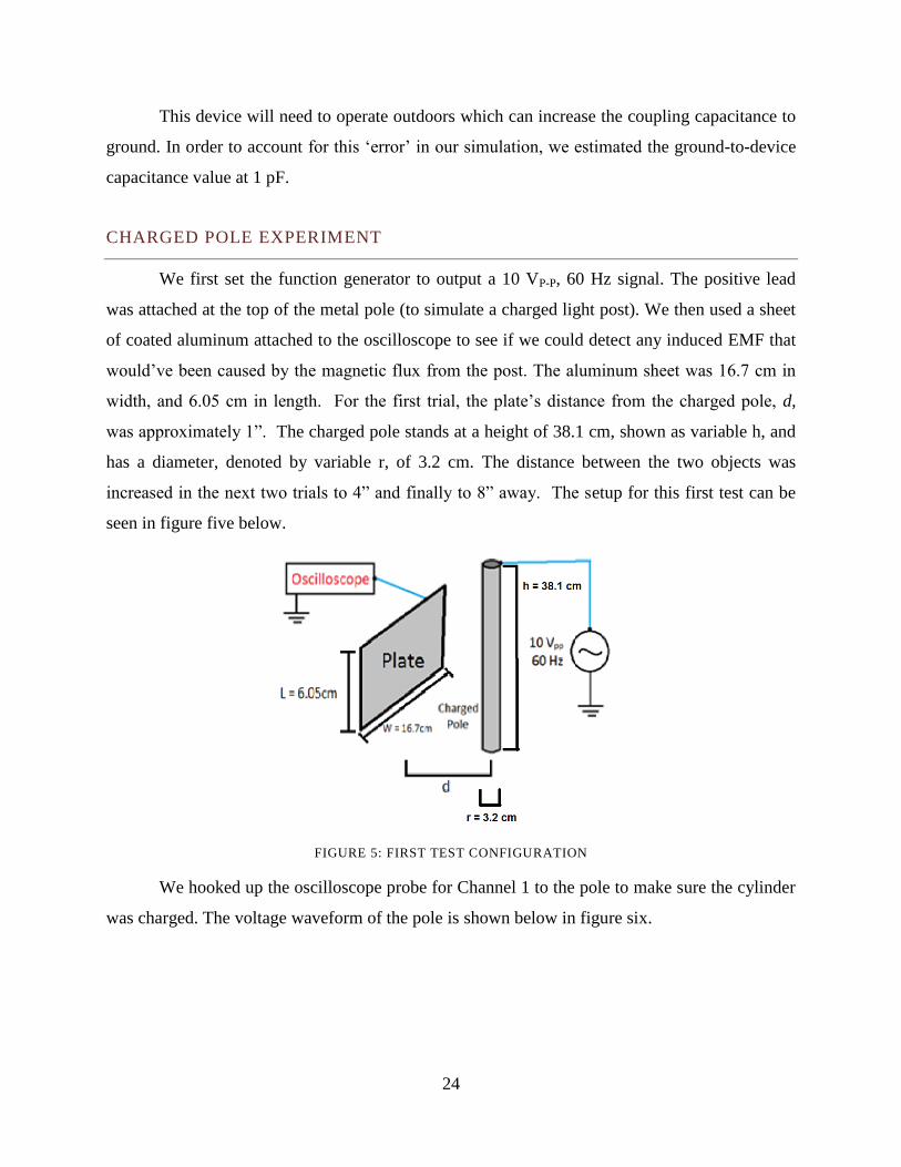
We hooked up the oscilloscope probe for Channel 1 to the pole to make sure the cylinder
was charged. The voltage waveform of the pole is shown below in figure six.
25
FIGURE 6: CHARGED POLE'S VOLTAGE WAVEFORM
The recorded peak-to-peak voltage was 10 V and the frequency was 59.9976 Hz (60Hz).
As the plate’s distance from the poke increased, a smaller voltage was recorded from the
oscilloscope.
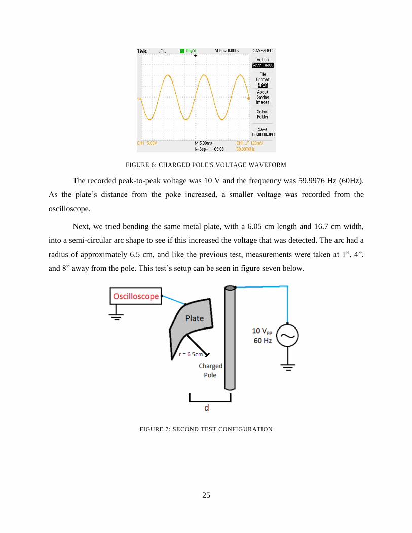
Next, we tried bending the same metal plate, with a 6.05 cm length and 16.7 cm width,
into a semi-circular arc shape to see if this increased the voltage that was detected. The arc had a
radius of approximately 6.5 cm, and like the previous test, measurements were taken at 1”, 4”,
and 8” away from the pole. This test’s setup can be seen in figure seven below.
FIGURE 7: SECOND TEST CONFIGURATION
26
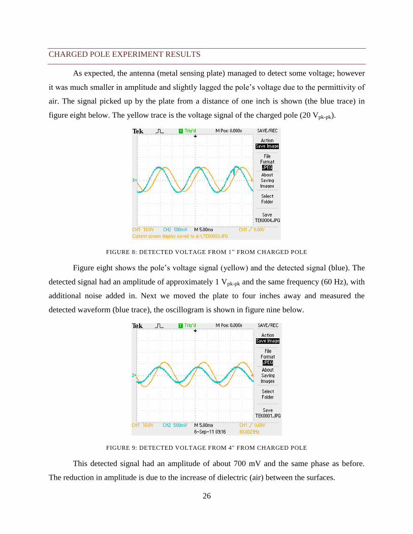
CHARGED POLE EXPERIMENT RESULTS
As expected, the antenna (metal sensing plate) managed to detect some voltage; however
it was much smaller in amplitude and slightly lagged the pole’s voltage due to the permittivity of
air. The signal picked up by the plate from a distance of one inch is shown (the blue trace) in
figure eight below. The yellow trace is the voltage signal of the charged pole (20 Vpk-pk).
FIGURE 8: DETECTED VOLTAGE FROM 1” FROM CHARGED POLE
Figure eight shows the pole’s voltage signal (yellow) and the detected signal (blue). The
detected signal had an amplitude of approximately 1 Vpk-pk and the same frequency (60 Hz), with
additional noise added in. Next we moved the plate to four inches away and measured the
detected waveform (blue trace), the oscillogram is shown in figure nine below.
FIGURE 9: DETECTED VOLTAGE FROM 4" FROM CHARGED POLE
This detected signal had an amplitude of about 700 mV and the same phase as before.
The reduction in amplitude is due to the increase of dielectric (air) between the surfaces.
27
We then tested the plate from a distance of eight inches away and the detected waveform
is shown in figure ten below.
FIGURE 10: DETECTED VOLTAGE FROM 8" FROM CHARGED POLE
Again, the detected voltage signal dropped to a peak-to-peak of about 500 mV and the
phase remained 60 Hz. We then tried bending the aluminum plate to make a concaved shape in
hopes that it could trap more of the electromagnetic radiation. The detected voltage was recorded
from distances of 1”, 4” and 8” and these oscillograms can be seen below in figures eleven,
twelve and thirteen respectively.
FIGURE 11: DETECTED VOLTAGE FROM 1” (WITH CURVED PLATE)
The curved plate still measured about a 1 V signal but with a lot of extra noise. The noise
frequency was around 1 kHz and only had an amplitude of 0.1 V. This noise interference was
likely caused by our contact with the plate while holding it. Typical fluorescent lighting and
screen refresh rates operate at similar frequencies so the computers and lighting in the testing lab
may have been the origin of this noise.
28
FIGURE 12: DETECTED VOLTAGE FROM 4” (WITH CURVED PLATE)
The waveform from 4” away had an amplitude of about 700 mV (similar to before).
FIGURE 13: DETECTED VOLTAGE FROM 8” (WITH CURVED PLATE)
The waveform from 8” away had an amplitude of about 500 mV (similar to before).The
curve in the plate did not seem to enhance the signal detection. The bend only added noise to an
already weak signal. The use of two separate plates is another option that will be considered and
possibly tested.
We found that it is possible to pick up electromagnetic radiation emitted from a charged
source using only a plate of aluminum. As the plate is moved away from the source its strength
decreases. Our experimentation has allowed us to pinpoint main design considerations: signal
detection and signal amplification.
PARALLEL PLATE EXPERIMENT
29
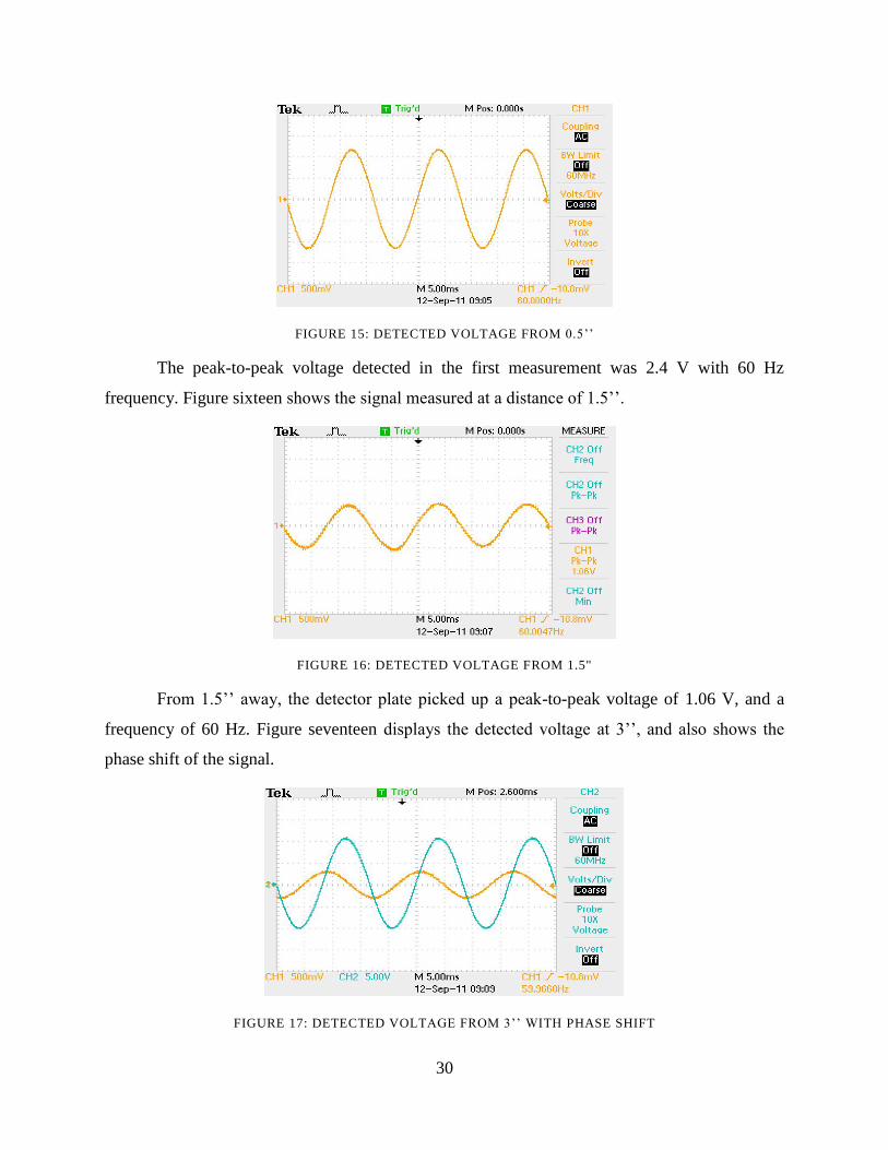
For our next experiment, we first set two aluminum plates to be parallel with one another.
We then set the function generator to output a 10 VPk-Pk, 60 Hz signal. The positive lead was
attached towards the bottom of the plate to be charged. The negative lead was connected to the
ground connection of the channel 1 oscilloscope probe, which was connected to the detection
plate. Next, we turned on the function generator, and used the oscilloscope to see if we could
detect any induced emf caused by the charged plate. The setup for this test can be seen in figure
fourteen below.
FIGURE 14: PARALLEL PLATE EXPERIMENT CONFIGURATION
With the set up complete, we began recording the peak-to-peak voltage detected by the
plate connected to the osciloscope at different distances. Initial measurements were taken whwen
the plates were 0.5’’ away from eachother. Additional measurements were taken at, 1’’, 1.5’’,
2’’, 3’’, 5’’, 7’’, 9’’, and 12’’ distances.
The detector plate picked up some emf from the charged plate, as we had anticipated.
Similar to the charged pole experiment, the detected voltage signal had a smaller amplitude,
especially as distance increased, and had a phase shift. Figure fifteen below displays the detected
signal from 0.5’’ away.
30
FIGURE 15: DETECTED VOLTAGE FROM 0.5’’
The peak-to-peak voltage detected in the first measurement was 2.4 V with 60 Hz
frequency. Figure sixteen shows the signal measured at a distance of 1.5’’.
FIGURE 16: DETECTED VOLTAGE FROM 1.5"
From 1.5’’ away, the detector plate picked up a peak-to-peak voltage of 1.06 V, and a
frequency of 60 Hz. Figure seventeen displays the detected voltage at 3’’, and also shows the
phase shift of the signal.
FIGURE 17: DETECTED VOLTAGE FROM 3’’ WITH PHASE SHIFT
31
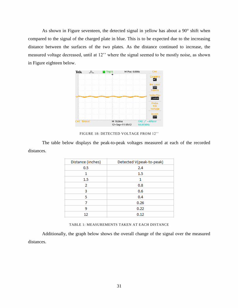
As shown in Figure seventeen, the detected signal in yellow has about a 90° shift when
compared to the signal of the charged plate in blue. This is to be expected due to the increasing
distance between the surfaces of the two plates. As the distance continued to increase, the
measured voltage decreased, until at 12’’ where the signal seemed to be mostly noise, as shown
in Figure eighteen below.
FIGURE 18: DETECTED VOLTAGE FROM 12’’
The table below displays the peak-to-peak voltages measured at each of the recorded
distances.
TABLE 1: MEASUREMENTS TAKEN AT EACH DISTANCE
Additionally, the graph below shows the overall change of the signal over the measured
distances.

32
As the graph indicates, the voltage detected decreases in strength as the plates move
farther away from each other. This is consistent with the results of the charged pole experiment.
Using two unshielded aluminum plates in parallel, we found that we could successfully
detect a voltage signal from about a foot away. Similar to the charged pole experiment, the
strength of the detected signal decreases as the plate was moved away from the source. With the
information gathered in this experiment and the charge pole experiment, we can begin to
incorporate signal amplification and noise filtering into the following stages of our project.
THE HUMAN IMPEDANCE TEST
In order to accurately represent our body’s resistance we conducted an experiment that
allowed us to estimate this value. In the test, one group member stood on the ground and with
one hand grabbed the end of a 120 V, 60 Hz live wire. A 1 MΩ resistor was used in between the
wire and the subject’s hand in order to limit the current and avoid possible injury. An analog
voltmeter was used to measure the voltage across the resistor and measurements were taking
with the subjects standing on concrete, grass and dirt. Using Ohm’s law, the voltage drop across
the subject’s body was calculated. The experiment setup is shown below with RX and CX
representing
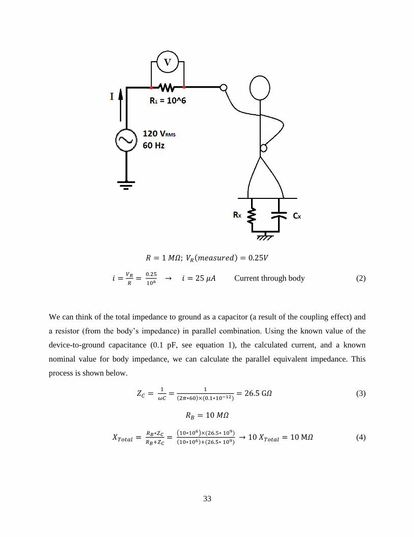
33
( )
Current through body (2)
We can think of the total impedance to ground as a capacitor (a result of the coupling effect) and
a resistor (from the body’s impedance) in parallel combination. Using the known value of the
device-to-ground capacitance (0.1 pF, see equation 1), the calculated current, and a known
nominal value for body impedance, we can calculate the parallel equivalent impedance. This
process is shown below.
( ) ( ) (3)
( ) ( )
( ) ( ) (4)
34
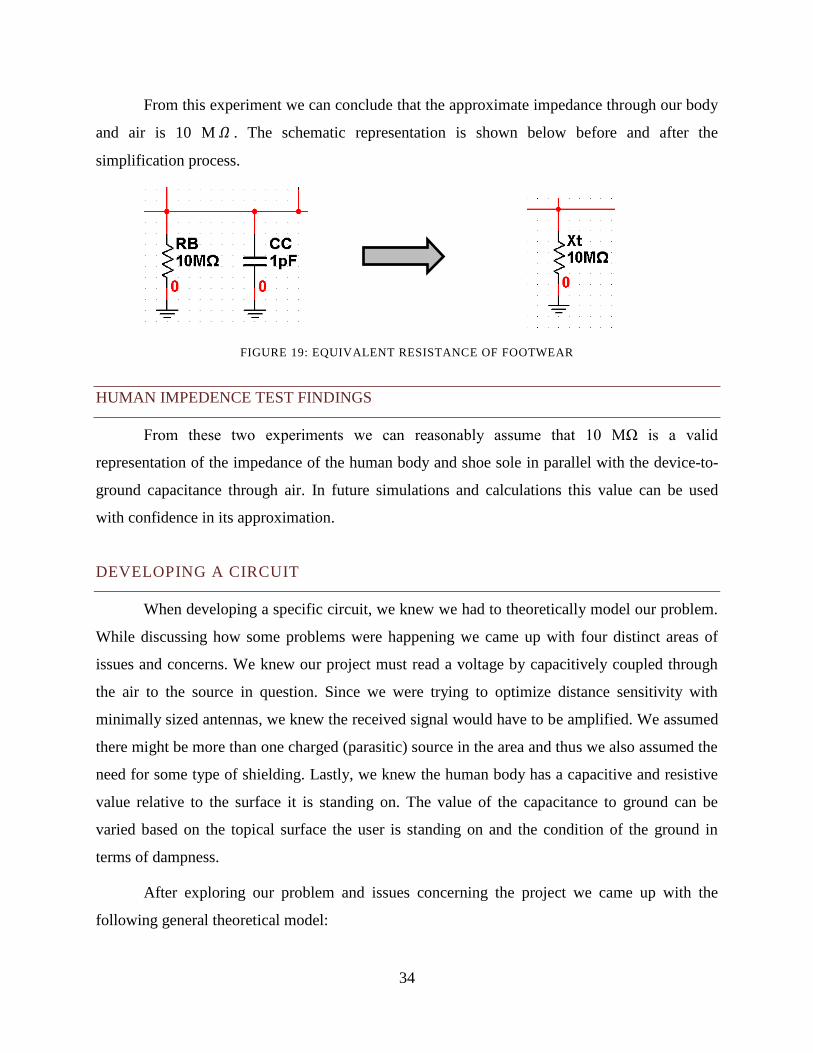
From this experiment we can conclude that the approximate impedance through our body
and air is 10 M . The schematic representation is shown below before and after the
simplification process.
FIGURE 19: EQUIVALENT RESISTANCE OF FOOTWEAR
HUMAN IMPEDENCE TEST FINDINGS
From these two experiments we can reasonably assume that 10 MΩ is a valid
representation of the impedance of the human body and shoe sole in parallel with the device-to-
ground capacitance through air. In future simulations and calculations this value can be used
with confidence in its approximation.
DEVELOPING A CIRCUIT
When developing a specific circuit, we knew we had to theoretically model our problem.
While discussing how some problems were happening we came up with four distinct areas of
issues and concerns. We knew our project must read a voltage by capacitively coupled through
the air to the source in question. Since we were trying to optimize distance sensitivity with
minimally sized antennas, we knew the received signal would have to be amplified. We assumed
there might be more than one charged (parasitic) source in the area and thus we also assumed the
need for some type of shielding. Lastly, we knew the human body has a capacitive and resistive
value relative to the surface it is standing on. The value of the capacitance to ground can be
varied based on the topical surface the user is standing on and the condition of the ground in
terms of dampness.
After exploring our problem and issues concerning the project we came up with the
following general theoretical model:
35
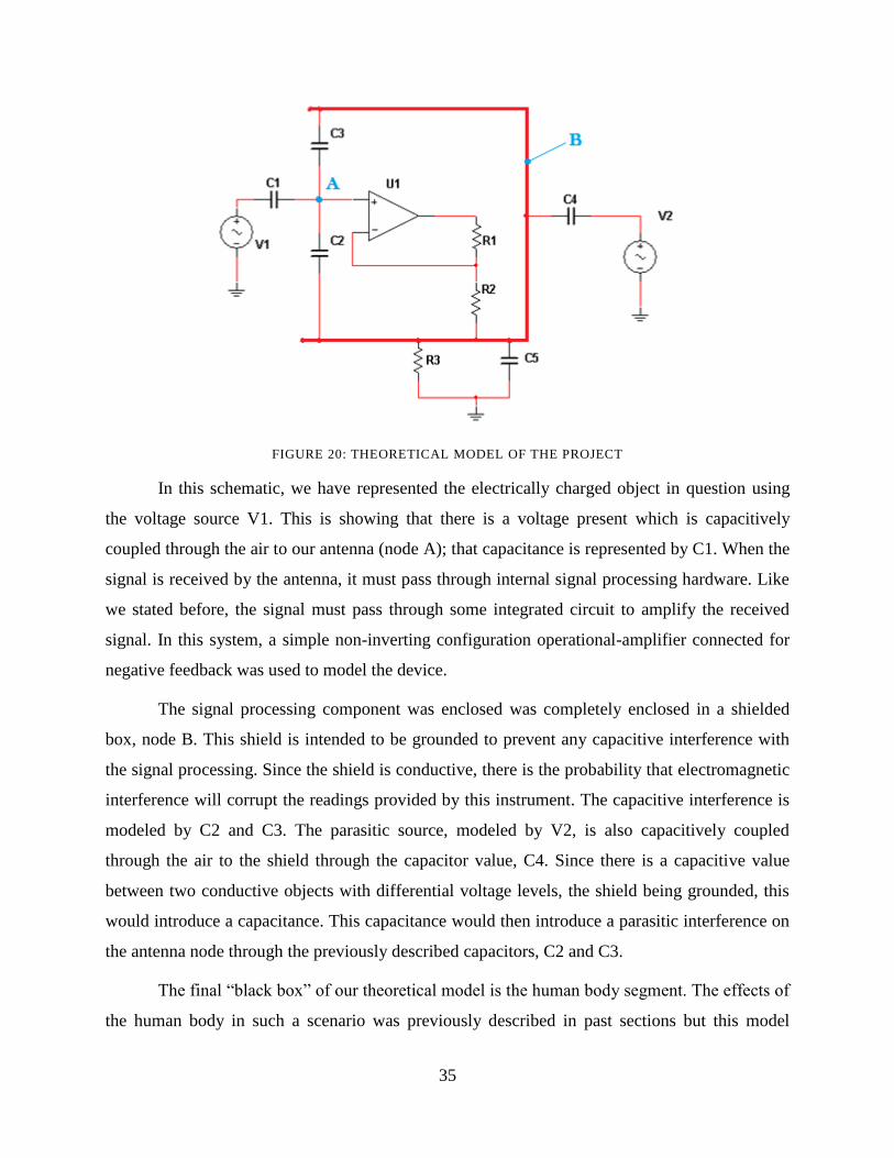
FIGURE 20: THEORETICAL MODEL OF THE PROJECT
In this schematic, we have represented the electrically charged object in question using
the voltage source V1. This is showing that there is a voltage present which is capacitively
coupled through the air to our antenna (node A); that capacitance is represented by C1. When the
signal is received by the antenna, it must pass through internal signal processing hardware. Like
we stated before, the signal must pass through some integrated circuit to amplify the received
signal. In this system, a simple non-inverting configuration operational-amplifier connected for
negative feedback was used to model the device.
The signal processing component was enclosed was completely enclosed in a shielded
box, node B. This shield is intended to be grounded to prevent any capacitive interference with
the signal processing. Since the shield is conductive, there is the probability that electromagnetic
interference will corrupt the readings provided by this instrument. The capacitive interference is
modeled by C2 and C3. The parasitic source, modeled by V2, is also capacitively coupled
through the air to the shield through the capacitor value, C4. Since there is a capacitive value
between two conductive objects with differential voltage levels, the shield being grounded, this
would introduce a capacitance. This capacitance would then introduce a parasitic interference on
the antenna node through the previously described capacitors, C2 and C3.
The final “black box” of our theoretical model is the human body segment. The effects of
the human body in such a scenario was previously described in past sections but this model
36
shows the exact correlation to our project. We know the human body has both a resistive and
capacitive value based on the relation to ground. With the user touching the grounded shield, we
are creating a parallel value of resistance and capacitance to ground.
With a better understanding of the problem at hand, we can begin to design a product that
can compensate for or eliminate the parasitic interference and how we can design the product to
be handheld yet sensitive enough to be used from a few meters away and work appropriately.
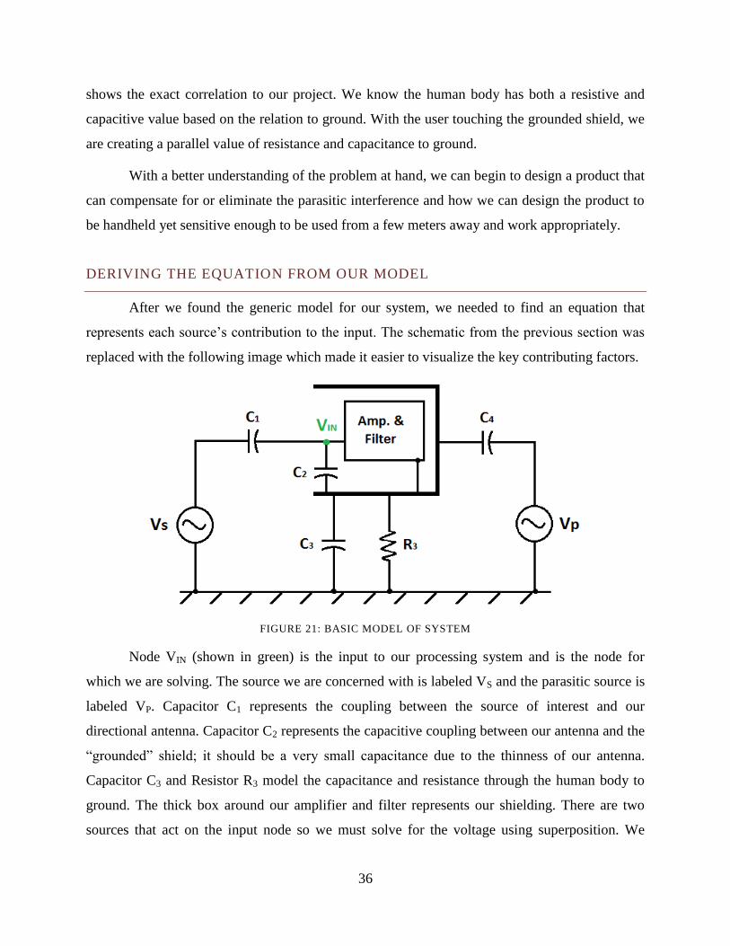
DERIVING THE EQUATION FROM OUR MODEL
After we found the generic model for our system, we needed to find an equation that
represents each source’s contribution to the input. The schematic from the previous section was
replaced with the following image which made it easier to visualize the key contributing factors.
FIGURE 21: BASIC MODEL OF SYSTEM
Node VIN (shown in green) is the input to our processing system and is the node for
which we are solving. The source we are concerned with is labeled VS and the parasitic source is
labeled VP. Capacitor C1 represents the coupling between the source of interest and our
directional antenna. Capacitor C2 represents the capacitive coupling between our antenna and the
“grounded” shield; it should be a very small capacitance due to the thinness of our antenna.
Capacitor C3 and Resistor R3 model the capacitance and resistance through the human body to
ground. The thick box around our amplifier and filter represents our shielding. There are two
sources that act on the input node so we must solve for the voltage using superposition. We
37
needed to zero out each source one at a time and calculate the voltage at VIN due to the remaining
source. The calculations and steps are shown below:
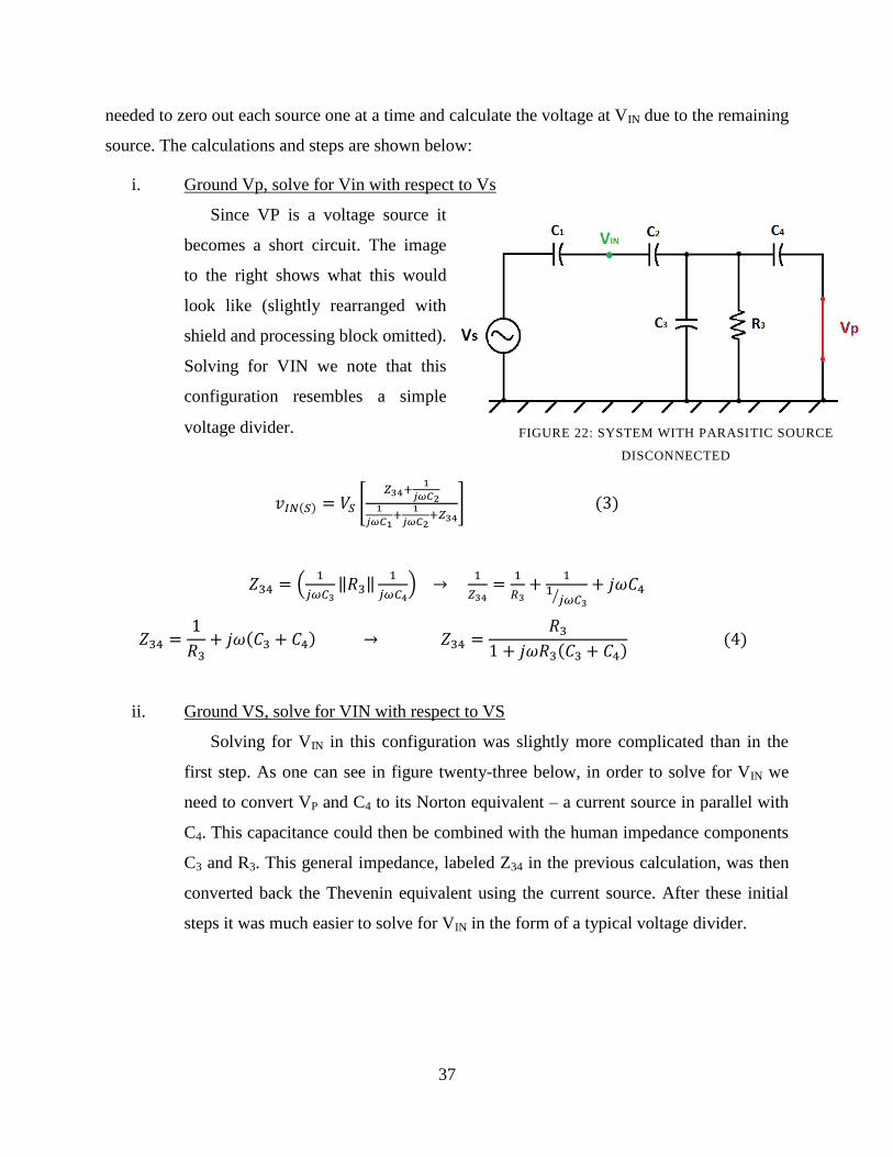
i. Ground Vp, solve for Vin with respect to Vs
Since VP is a voltage source it
becomes a short circuit. The image
to the right shows what this would
look like (slightly rearranged with
shield and processing block omitted).
Solving for VIN we note that this
configuration resembles a simple
voltage divider.
( ) [
] ( )
(
‖ ‖
)
⁄
( )
( )
( )
ii. Ground VS, solve for VIN with respect to VS
Solving for VIN in this configuration was slightly more complicated than in the
first step. As one can see in figure twenty-three below, in order to solve for VIN we
need to convert VP and C4 to its Norton equivalent – a current source in parallel with
C4. This capacitance could then be combined with the human impedance components
C3 and R3. This general impedance, labeled Z34 in the previous calculation, was then
converted back the Thevenin equivalent using the current source. After these initial
steps it was much easier to solve for VIN in the form of a typical voltage divider.
FIGURE 22: SYSTEM WITH PARASITIC SOURCE
DISCONNECTED
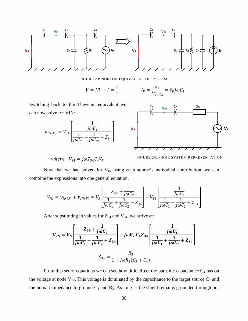
38
⁄
Switching back to the Thevenin equivalent we
can now solve for VIN:
( ) [
]
Now that we had solved for VIN using each source’s individual contribution, we can
combine the expressions into one general equation.
( ) ( ) [
] [
]
After substituting in values for Z34 and V34, we arrive at:
[
] [
]
( )
From this set of equations we can see how little effect the parasitic capacitance C4 has on
the voltage at node VIN. This voltage is dominated by the capacitance to the target source C1 and
the human impedance to ground C3 and R3. As long as the shield remains grounded through our
FIGURE 23: NORTON EQUIVALENT OF SYSTEM
FIGURE 24: FINAL SYSTEM REPRESENTATION

39
body and the antenna is directed at the target source, the parasitic voltage source will have a
negligible effect on our reading.
The following charts shows the effects of the parasitic capacitance’s influence on the
node .
FIGURE 25:SCATTER PLOTS OF VOLTAGE BASED ON CAPACITANCE
FIGURE 26:EXCEL SPREADSHEET FOR THE CHART ABOVE
0
20
40
60
80
100
120
140
0.00010.0010.010.11101001000
Vo
lta
ge
at
An
ten
na
(V
)
Capacitance to Antenna (fF)
Change in Voltage Over
Capacitance
40
[
] [
]
FIGURE 27: EQUATION USED TO CALCULATE NUMBERS
From chart above in figure twenty-five we can recognize the effects of the parasitic
source and how it influences our output. In the graph, the line marked with triangles represents
the value of our input without the effects of the parasitic capacitance. This allows us to witness
as the distance grows and the value of the capacitance decreases, so does the value of the
voltage. The line marked with squares represents the effects of the parasitic source when the
parasitic source is far greater than the capacitance in question. This allows the antenna to receive
a great amount of parasitic influence and would over power the signal we were attempting to
obtain. Finally, there is one other line located underneath the triangle line. This represents the
value of the parasitic capacitance being approximately equal to our capacitance in question. But
from this graph you can see as long as the capacitance from the parasitic source is much larger,
our reading will prove to be approximately true. The error percentage from the ideal to the best
cases is always less than three percent for the data marks taken
INVERTING VS. NON-INVERTING CONFIGURATIONS
When implementing an operational amplifier, you can configure the integrated circuit
(IC) to be an inverting or non-inverting configuration. In our schematic, we were left to weigh
the pros and cons of each configuration in order to choose the best implementation for our
design. We first assumed we would need a configuration with low input impedance in order to
reduce consumption through our system. For this matter, we would choose an inverting
configuration. From the figure below, you can see the generic configuration of an inverting
operational amplifier connected for negative feedback.
41
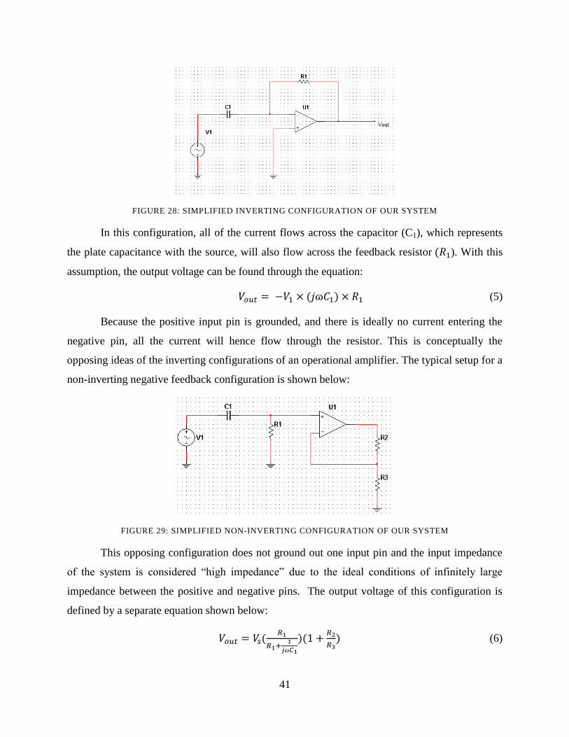
FIGURE 28: SIMPLIFIED INVERTING CONFIGURATION OF OUR SYSTEM
In this configuration, all of the current flows across the capacitor (C1), which represents
the plate capacitance with the source, will also flow across the feedback resistor ( ). With this
assumption, the output voltage can be found through the equation:
( ) (5)
Because the positive input pin is grounded, and there is ideally no current entering the
negative pin, all the current will hence flow through the resistor. This is conceptually the
opposing ideas of the inverting configurations of an operational amplifier. The typical setup for a
non-inverting negative feedback configuration is shown below:
FIGURE 29: SIMPLIFIED NON-INVERTING CONFIGURATION OF OUR SYSTEM
This opposing configuration does not ground out one input pin and the input impedance
of the system is considered “high impedance” due to the ideal conditions of infinitely large
impedance between the positive and negative pins. The output voltage of this configuration is
defined by a separate equation shown below:
(
)(
) (6)

42
From these two options of configurations, we chose the non-inverting configuration
because of its ability to accept gain to the output. Since we can assume the frequency and
capacitance will be constant (60 Hz due to national power frequency and capacitance based on
distance given a receiving plate size) we will have better control on the gain while still biasing
the input pin. We know the inverting and non-inverting pins of the op-amp, when connected for
negative feedback will drive them to be equal. In the inverting configurations, we are cutting out
one entire side of the oscillation spectrum. If we use the non-inverting configuration, we can
control the DC-bias based on a single supply operational amplifier. This will be further explained
in the coming sections.
JFET VS. CMOS AMPLIFIER
When choosing a specific IC chip, there are various styles of chips that can yield the
same results. When first conducting the experimental configurations we had utilized the TL081
IC chip manufactured by Texas Instruments. The chip is a JFET input stage IC chip. One reason
for choosing this IC chip was based on ease of access and to model the schematic suggested by
Professor Bitar. After some research, we realized a CMOS op-amp would fare better.
Based on comparison, the CMOS and JFET have some common useful perks. Both
designs have capabilities to run off a single source and have very low current-noise density (each
around 0.5fA/√ ). But we have learned the JFET allows for greater Voltage-Noise density.
When examining the CMOS input stage amplifiers, we learned they allow for greater voltage
spectrums. JFET usually reduces the ability for the output voltages to reach full “rail potentials”.
JFET usually limit within 1-1.5 volts of the rails. CMOS allows for greater utilizations of the
output capabilities. The CMOS also offers lower input-bias currents, voltage offset, and
distortion. They also specialize in voltage-noise density, low-input current-noise density, and
current-noise performance (MAXIM).
SCHEMATIC
The following schematic is the working schematic of our system. It is a primary design
which all components are not finalize, but the one we will use in order to conduct robust
experiments. Please see the image below for our design; all blue icons were actual components in
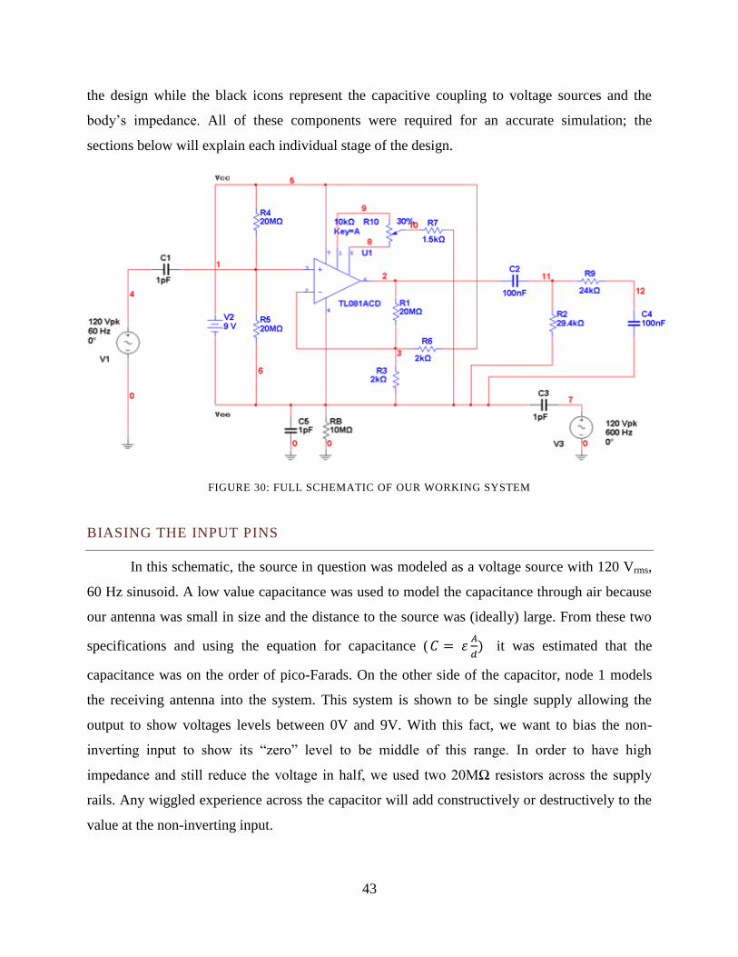
43
the design while the black icons represent the capacitive coupling to voltage sources and the
body’s impedance. All of these components were required for an accurate simulation; the
sections below will explain each individual stage of the design.
FIGURE 30: FULL SCHEMATIC OF OUR WORKING SYSTEM
BIASING THE INPUT PINS
In this schematic, the source in question was modeled as a voltage source with 120 Vrms,
60 Hz sinusoid. A low value capacitance was used to model the capacitance through air because
our antenna was small in size and the distance to the source was (ideally) large. From these two
specifications and using the equation for capacitance (
) it was estimated that the
capacitance was on the order of pico-Farads. On the other side of the capacitor, node 1 models
the receiving antenna into the system. This system is shown to be single supply allowing the
output to show voltages levels between 0V and 9V. With this fact, we want to bias the non-
inverting input to show its “zero” level to be middle of this range. In order to have high
impedance and still reduce the voltage in half, we used two 20MΩ resistors across the supply
rails. Any wiggled experience across the capacitor will add constructively or destructively to the
value at the non-inverting input.

44
The same mechanism was used at the output. From the positive power supply to the
circuit ground there is low impedance biasing the inverting input terminal. By combining two
2kΩ resistors in parallel to the 1MΩ resistor on the output, we set the Thevenized equivalent
resistance to 1kΩ. This sets the gain ratio to be approximately 1000. By connecting the inverting
input to the middle of these two resistors, this also biases the inverting input to equal the non-
inverting input. Once again, the wiggle experienced by the non-inverting input will be shown
and compensated for at the inverting input.
ZEROING THE OFFSET
You will notice between pins 1 and 5, there is a potentiometer and an additional resistor
connected to ground. The potentiometer is used to rid the operational amplifier of its offset
voltage. The offset voltages are usually set to tolerate up to 6 mV. In this system, this 6 mV of
offset will show as 6 V on the output when multiplied by the gain of 1000. This output voltage
will limit the amount of voltage we can read on the output. By installing a potentiometer, we will
be able to zero the offset giving our system the best chance to show the signal through. The
additional resistor is added in order to improve the resolution of the potentiometer as well as
limit the value of the resistance across the pins.
FILTERING
Through our circuit we experienced a few instances of interference. Even though our
shield is grounded, we are still experiencing stray frequencies. These unexpected frequencies are
usually accredited to static motion from feet scuffing the carpet, refresh rates from the screens of
nearby monitors, or stray voltages from higher frequency machines. In order to reduce these
effects we needed to install some sort of filtering within our system. In our schematic above, we
modeled the interference source as a 600 Hz source. This value was great enough for use to see
visibly the effects of the parasitic source.
In order for our filter to work effectively, we must neglect low and high parasitic
frequencies. We know we are able to focus on a 60 Hz source since our national standard is 60
Hz. With these facts, we decided to implement a bandpass filter made up of a low pass and high
pass filter. The frequencies of the cutoffs are found by the equation below:

45
(7)
By implementing a low pass filter followed by a high pass filter, we are able to
effectively manipulate a band pass filter. Our design sets the high pass filter to pass frequencies
of 55 Hz or greater and the low pass filter is designed to kill any frequencies greater than 65 Hz.
This filter configuration can be found off of the output of the op-amp.
ASSEMBLY OF THE DETECTOR
The construction of our device revolved around our choice of antenna shielding, which
was electrical conduit piping made from galvanized steel. It was then decided that the most
fitting design for the detector would be something similar to a radar gun. With that in mind, we
began to gather materials to make a handle and to attach it to the pipe, and to hold our circuit
board inside the pipe.
First, small metal rods, which were cut to the length of the pipe, were bolted to the inside
of the pipe to allow the circuit board to be slid into position underneath. To give us the ability to
adjust the potentiometer used to zero the offset voltage of the amplifier, a hole small enough to
fit the end of a screwdriver into was drilled out of the pipe.
For the handle, we customized an airsoft gun foregrip so that it could hold a 9V battery.
To do this, we filed out the center of the foregrip, which initially held an insert that could be
screwed in, so that a 9V battery could slide in easily. The screw insert was then cut down so that
it could hold the battery in place. We then cut out a small section towards the top of the grip to
insert our trigger; a switch which would turn the device on so long as the button was held down.
A 9V battery clip was attached to the trigger, as well as hot and ground leads, which had a
female connector at the end to plug the wires into the circuit.
To attach the handle to the pipe, we had a plastic piece made to fit the contours already
provided by the handle. The piece was modeled in the SolidWorks design program, and a rapid
prototype of the model was created. A hole in the center of the piece was also cut out so that the
leads from the handle could be inserted into the pipe. So, in addition to the holes drilled into the
pipe for the two screws that would attach the plastic piece, another hole similar to the hole cut
out of the plastic piece was cut out of the pipe. The plastic piece was then screwed onto the pipe.
46
The handle was then attached to the pipe once the plastic piece was attached, and the hot
and ground leads from the trigger were fed through the hole at the top of the hand and into the
inside of the pipe. Before inserting the circuit, the bottom of the PCB was covered with a
nonconductive tape to protect the exposed component leads of the board from the pipe shielding.
We then plugged in the wires from the handle into the circuit board, and slid it into place so that
the antenna would rest at about 1cm from the operating end of the device. To ground the board
to the shielding, we attached another ground wire to the board with an insulated ring connector,
which was then fit onto one of the screws from the plastic piece with a nut screwed in over it. A
small hole was then drilled though the center of the steel pipe end cap so that the output wire of
the circuit could be put through. Finally, the end cap was screwed into place at the end of the
device.
METHODOLOGY
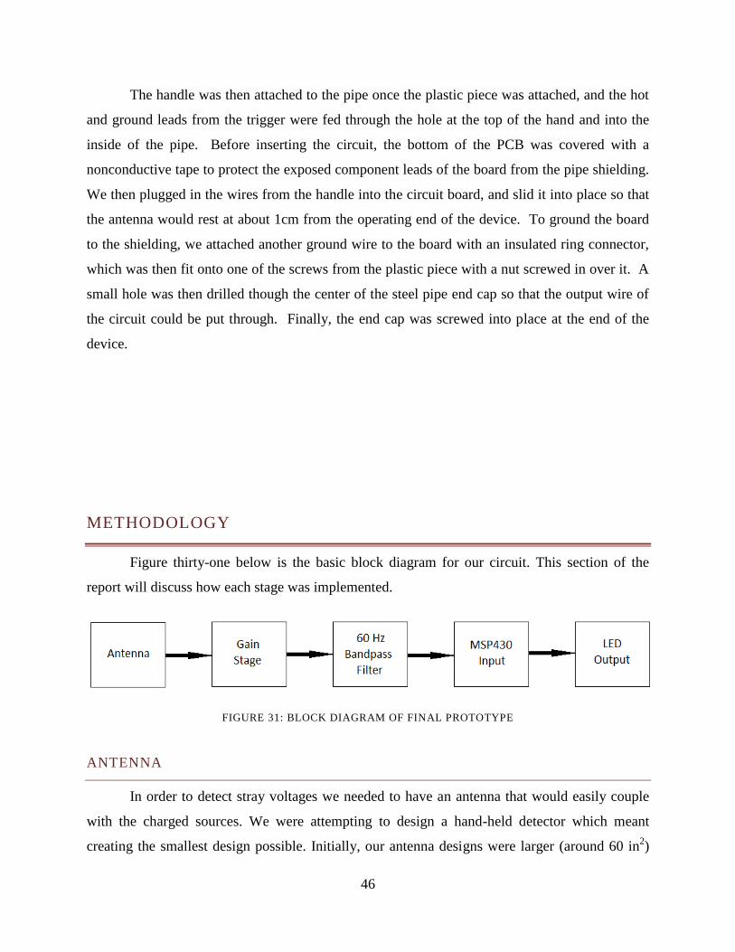
Figure thirty-one below is the basic block diagram for our circuit. This section of the
report will discuss how each stage was implemented.
FIGURE 31: BLOCK DIAGRAM OF FINAL PROTOTYPE
ANTENNA
In order to detect stray voltages we needed to have an antenna that would easily couple
with the charged sources. We were attempting to design a hand-held detector which meant
creating the smallest design possible. Initially, our antenna designs were larger (around 60 in2)
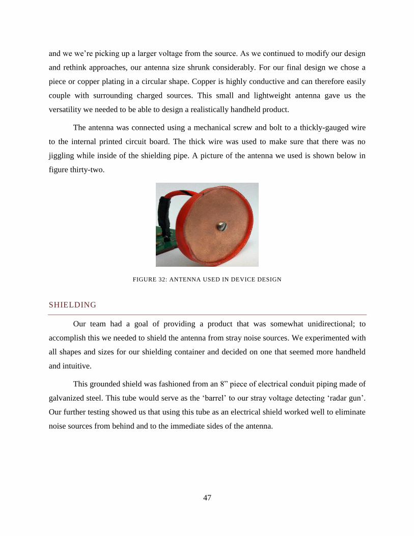
47
and we we’re picking up a larger voltage from the source. As we continued to modify our design
and rethink approaches, our antenna size shrunk considerably. For our final design we chose a
piece or copper plating in a circular shape. Copper is highly conductive and can therefore easily
couple with surrounding charged sources. This small and lightweight antenna gave us the
versatility we needed to be able to design a realistically handheld product.
The antenna was connected using a mechanical screw and bolt to a thickly-gauged wire
to the internal printed circuit board. The thick wire was used to make sure that there was no
jiggling while inside of the shielding pipe. A picture of the antenna we used is shown below in
figure thirty-two.
FIGURE 32: ANTENNA USED IN DEVICE DESIGN
SHIELDING
Our team had a goal of providing a product that was somewhat unidirectional; to
accomplish this we needed to shield the antenna from stray noise sources. We experimented with
all shapes and sizes for our shielding container and decided on one that seemed more handheld
and intuitive.
This grounded shield was fashioned from an 8” piece of electrical conduit piping made of
galvanized steel. This tube would serve as the ‘barrel’ to our stray voltage detecting ‘radar gun’.
Our further testing showed us that using this tube as an electrical shield worked well to eliminate
noise sources from behind and to the immediate sides of the antenna.
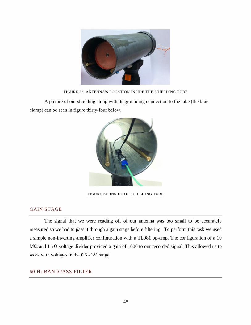
48
FIGURE 33: ANTENNA'S LOCATION INSIDE THE SHIELDING TUBE
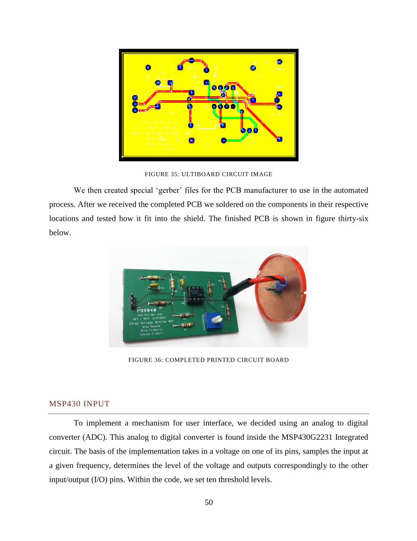
A picture of our shielding along with its grounding connection to the tube (the blue
clamp) can be seen in figure thirty-four below.
FIGURE 34: INSIDE OF SHIELDING TUBE
GAIN STAGE
The signal that we were reading off of our antenna was too small to be accurately
measured so we had to pass it through a gain stage before filtering. To perform this task we used
a simple non-inverting amplifier configuration with a TL081 op-amp. The configuration of a 10
MΩ and 1 kΩ voltage divider provided a gain of 1000 to our recorded signal. This allowed us to
work with voltages in the 0.5 - 3V range.
60 HZ BANDPASS FILTER

49
To implement a 60 Hz bandpass filter we used a common low pass filter followed by a
high pass filter. The bandwidth for the filter was set using the resistor and capacitor values, and
chosen to be 10 Hz centered on the target frequency of 60 Hz.
To implement the low pass filter we used a capacitor and a resistor in parallel
combination with the resistor terminating to ground. To calculate the cutoff frequency of the low
pass filter we used the relation described before;
. Substituting in the chosen values of
100 nF for the capacitor and 29 kΩ for the resistor we obtain:
( ) ( )
Similarly to make the high pass filter we used a resistor in parallel combination with a
capacitor terminating to ground. And once again, to calculate the cutoff frequency using our
chosen values of 100 nF for the capacitor and 29 kΩ for the resistor we obtain:
( ) ( )
This bandpass filter performs ideally and its output supplies the filtered input signal to the
MSP430 microprocessor. In hindsight, we would’ve added a unity gain buffer at the output or in
between each filtering stage in order to provide more current to the microprocessor.
CREATING A PRINTED CIRCUIT BOARD
In order for our circuit to fit inside the shielding pipe, we need to create a custom printed
circuit board (PCB) with the exact dimensions required. To convert our schematic into a board
design file we used UltiBoard, a program designed to work in conjunction with MultiSim in this
process. We measured the track width inside the shielding pipe with calipers to find the desired
width for the PCB. In Ultiboard, we customized the width and length of the board and laid out
the components in an intuitive and neat pattern.
50
FIGURE 35: ULTIBOARD CIRCUIT IMAGE
We then created special ‘gerber’ files for the PCB manufacturer to use in the automated
process. After we received the completed PCB we soldered on the components in their respective
locations and tested how it fit into the shield. The finished PCB is shown in figure thirty-six
below.
FIGURE 36: COMPLETED PRINTED CIRCUIT BOARD
MSP430 INPUT
To implement a mechanism for user interface, we decided using an analog to digital
converter (ADC). This analog to digital converter is found inside the MSP430G2231 Integrated
circuit. The basis of the implementation takes in a voltage on one of its pins, samples the input at
a given frequency, determines the level of the voltage and outputs correspondingly to the other
input/output (I/O) pins. Within the code, we set ten threshold levels.

51
The ADC works on interrupts rather than embedded coding. This means, every 10 kHz
the program will pause from its code and perform an ADC reading, retrieve the value of the
sample, and proceed with the code. When the ADC reads in 20 samples, there is a code that will
read the average and determine which threshold it belongs to. This threshold value correlates to a
given 4 bit output code. The average value code is shown below:
while(1) average=0; //initalize the energy to 0 for(i=0;i<window;i++) average= average +(data[i]); //add all the array elements together average=average/window; Warn(average);
When this program executes, the code then performs the code for the function warn. The
following function performs this task:
void Warn(int averageADC) if (averageADC > threshold10) //setting thresholds Highest to lowest. P1OUT=BIT4 + BIT2; //Setting outputs to decoder else if (averageADC > threshold9) P1OUT= BIT4 + BIT1; else if (averageADC > threshold8) //the error would be only if the bit one is lit up. get rid of else and just if P1OUT= BIT4; else if (averageADC > threshold7) // then add breaks. P1OUT= BIT3 + BIT2 +BIT1; else if (averageADC > threshold6) P1OUT= BIT3 + BIT2; else if (averageADC > threshold5) P1OUT= BIT3 + BIT1; else if (averageADC > threshold4) P1OUT= BIT3; else if (averageADC > threshold3) P1OUT= BIT2 + BIT1; else if (averageADC > threshold2) P1OUT= BIT2; else if (averageADC > threshold1) P1OUT= BIT1;
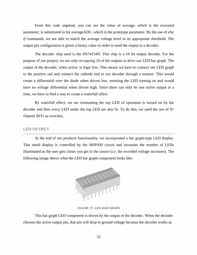
52
From this code segment, you can see the value of average, which is the executed
parameter, is substituted in for averageADC, which is the prototype parameter. By the use of else
if commands, we are able to match the average voltage level to its appropriate threshold. The
output pin configuration is given a binary value in order to send the output to a decoder.
The decoder chip used is the SN74154N. This chip is a 16 bit output decoder. For the
purpose of our project, we are only occupying 10 of the outputs to drive our LED bar graph. The
output of the decoder, when active, is logic low. This means we have to connect our LED graph
to the positive rail and connect the cathode end to our decoder through a resistor. This would
create a differential over the diode when driven low, ensuring the LED turning on and would
have no voltage differential when driven high. Since there can only be one active output at a
time, we have to find a way to create a waterfall effect.
By waterfall effect, we are insinuating the top LED of operation is turned on by the
decoder and then every LED under the top LED are also lit. To do this, we used the use of N-
channel BJTs as switches.
LED OUTPUT
At the end of our products functionality, we incorporated a bar graph-type LED display.
This small display is controlled by the MSP430 circuit and increases the number of LEDs
illuminated as the user gets closer you get to the source (i.e. the recorded voltage increases). The
following image shows what the LED bar graph component looks like:
FIGURE 37: LED BAR GRAPH
This bar graph LED component is driven by the output of the decoder. When the decoder
chooses the active output pin, that pin will drop to ground voltage because the decoder works as
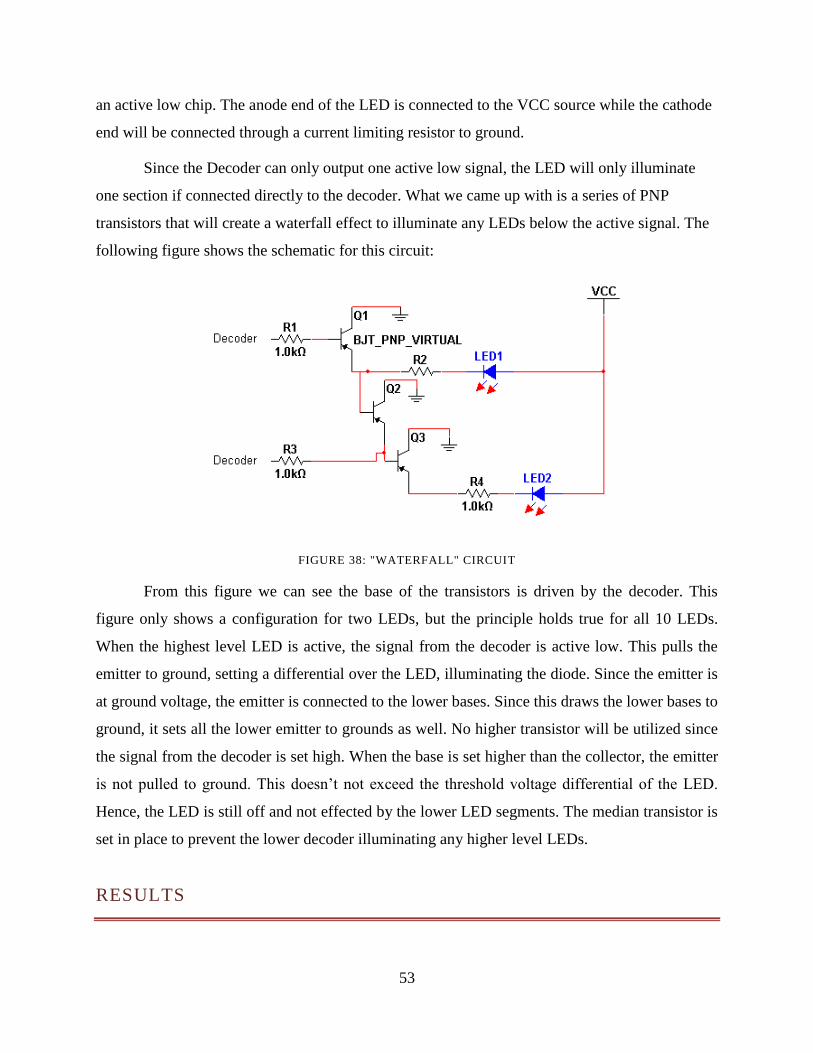
53
an active low chip. The anode end of the LED is connected to the VCC source while the cathode
end will be connected through a current limiting resistor to ground.
Since the Decoder can only output one active low signal, the LED will only illuminate
one section if connected directly to the decoder. What we came up with is a series of PNP
transistors that will create a waterfall effect to illuminate any LEDs below the active signal. The
following figure shows the schematic for this circuit:
FIGURE 38: "WATERFALL" CIRCUIT
From this figure we can see the base of the transistors is driven by the decoder. This
figure only shows a configuration for two LEDs, but the principle holds true for all 10 LEDs.
When the highest level LED is active, the signal from the decoder is active low. This pulls the
emitter to ground, setting a differential over the LED, illuminating the diode. Since the emitter is
at ground voltage, the emitter is connected to the lower bases. Since this draws the lower bases to
ground, it sets all the lower emitter to grounds as well. No higher transistor will be utilized since
the signal from the decoder is set high. When the base is set higher than the collector, the emitter
is not pulled to ground. This doesn’t not exceed the threshold voltage differential of the LED.
Hence, the LED is still off and not effected by the lower LED segments. The median transistor is
set in place to prevent the lower decoder illuminating any higher level LEDs.
RESULTS
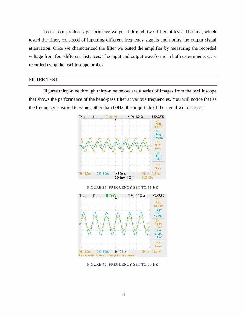
54
To test our product’s performance we put it through two different tests. The first, which
tested the filter, consisted of inputting different frequency signals and noting the output signal
attenuation. Once we characterized the filter we tested the amplifier by measuring the recorded
voltage from four different distances. The input and output waveforms in both experiments were
recorded using the oscilloscope probes.
FILTER TEST
Figures thirty-nine through thirty-nine below are a series of images from the oscilloscope
that shows the performance of the band-pass filter at various frequencies. You will notice that as
the frequency is varied to values other than 60Hz, the amplitude of the signal will decrease.
FIGURE 39: FREQUENCY SET TO 15 HZ
FIGURE 40: FREQUENCY SET TO 60 HZ
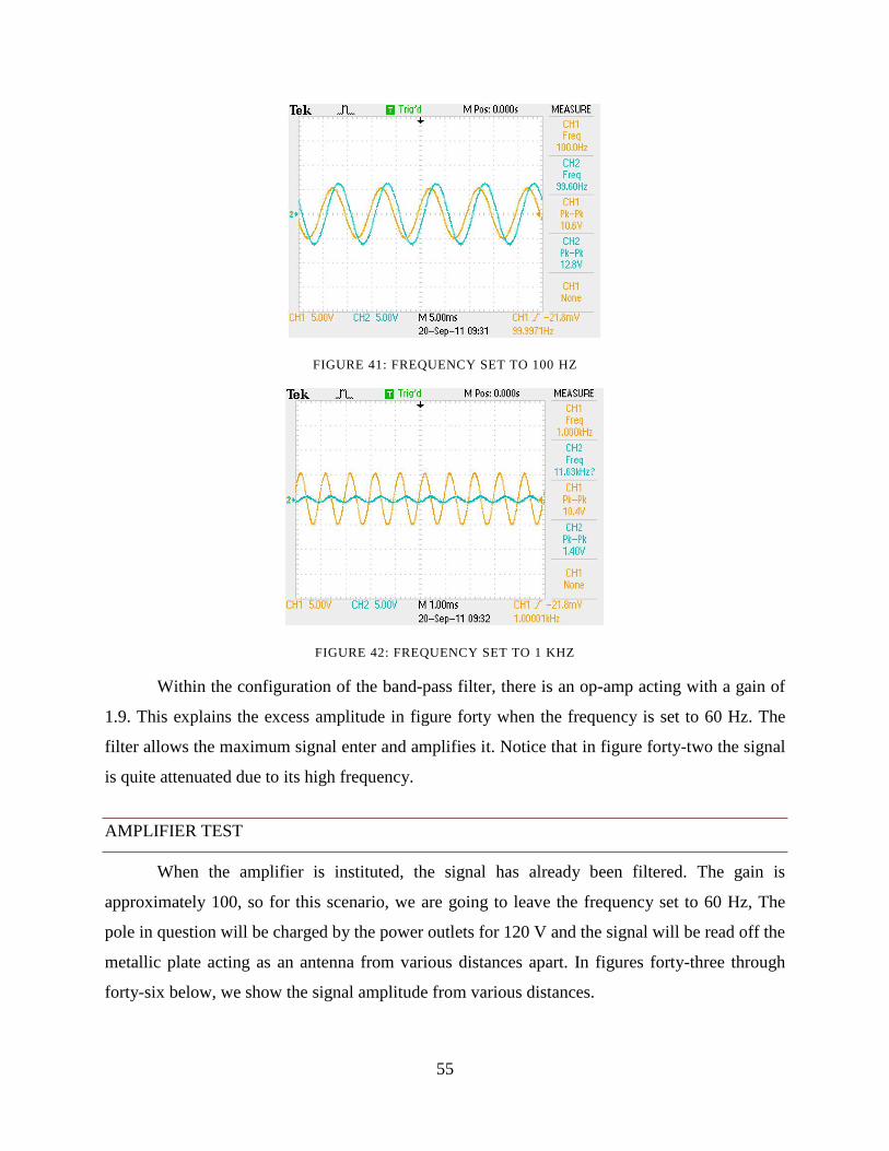
55
FIGURE 41: FREQUENCY SET TO 100 HZ
FIGURE 42: FREQUENCY SET TO 1 KHZ
Within the configuration of the band-pass filter, there is an op-amp acting with a gain of
1.9. This explains the excess amplitude in figure forty when the frequency is set to 60 Hz. The
filter allows the maximum signal enter and amplifies it. Notice that in figure forty-two the signal
is quite attenuated due to its high frequency.
AMPLIFIER TEST
When the amplifier is instituted, the signal has already been filtered. The gain is
approximately 100, so for this scenario, we are going to leave the frequency set to 60 Hz, The
pole in question will be charged by the power outlets for 120 V and the signal will be read off the
metallic plate acting as an antenna from various distances apart. In figures forty-three through
forty-six below, we show the signal amplitude from various distances.
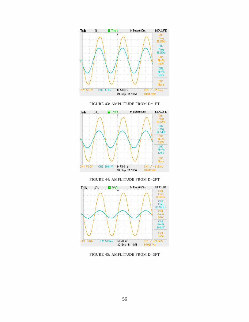
56
FIGURE 43: AMPLITUDE FROM D=1FT
FIGURE 44: AMPLITUDE FROM D=2FT
FIGURE 45: AMPLITUDE FROM D=3FT
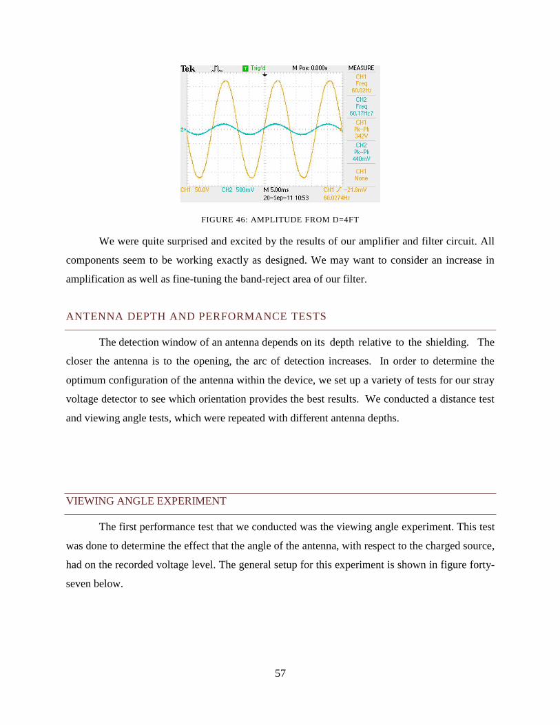
57
FIGURE 46: AMPLITUDE FROM D=4FT
We were quite surprised and excited by the results of our amplifier and filter circuit. All
components seem to be working exactly as designed. We may want to consider an increase in
amplification as well as fine-tuning the band-reject area of our filter.
ANTENNA DEPTH AND PERFORMANCE TESTS
The detection window of an antenna depends on its depth relative to the shielding. The
closer the antenna is to the opening, the arc of detection increases. In order to determine the
optimum configuration of the antenna within the device, we set up a variety of tests for our stray
voltage detector to see which orientation provides the best results. We conducted a distance test
and viewing angle tests, which were repeated with different antenna depths.
VIEWING ANGLE EXPERIMENT
The first performance test that we conducted was the viewing angle experiment. This test
was done to determine the effect that the angle of the antenna, with respect to the charged source,
had on the recorded voltage level. The general setup for this experiment is shown in figure forty-
seven below.
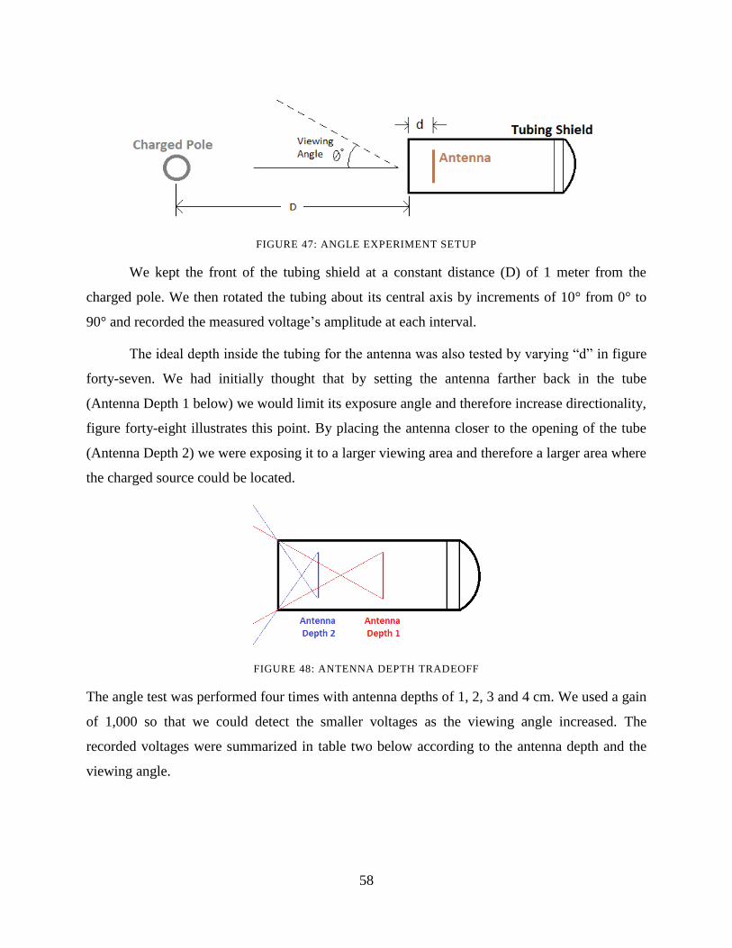
58
FIGURE 47: ANGLE EXPERIMENT SETUP
We kept the front of the tubing shield at a constant distance (D) of 1 meter from the
charged pole. We then rotated the tubing about its central axis by increments of 10° from 0° to
90° and recorded the measured voltage’s amplitude at each interval.
The ideal depth inside the tubing for the antenna was also tested by varying “d” in figure
forty-seven. We had initially thought that by setting the antenna farther back in the tube
(Antenna Depth 1 below) we would limit its exposure angle and therefore increase directionality,
figure forty-eight illustrates this point. By placing the antenna closer to the opening of the tube
(Antenna Depth 2) we were exposing it to a larger viewing area and therefore a larger area where
the charged source could be located.
FIGURE 48: ANTENNA DEPTH TRADEOFF
The angle test was performed four times with antenna depths of 1, 2, 3 and 4 cm. We used a gain
of 1,000 so that we could detect the smaller voltages as the viewing angle increased. The
recorded voltages were summarized in table two below according to the antenna depth and the
viewing angle.
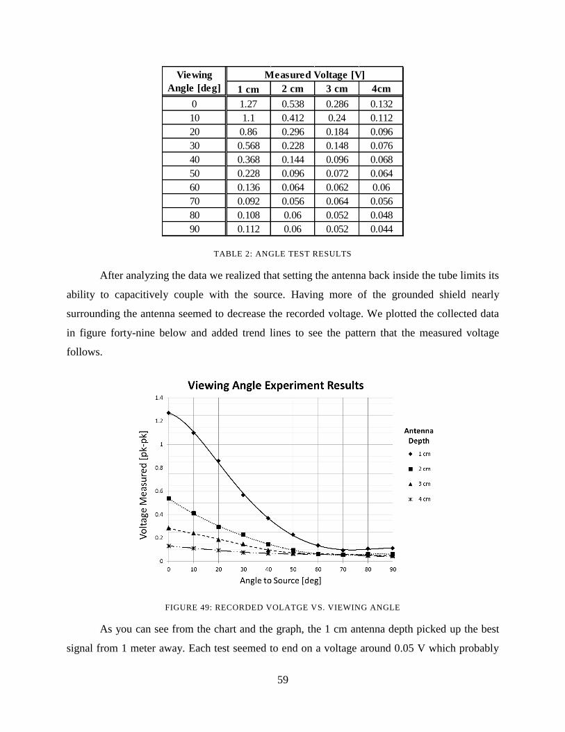
59
TABLE 2: ANGLE TEST RESULTS
After analyzing the data we realized that setting the antenna back inside the tube limits its
ability to capacitively couple with the source. Having more of the grounded shield nearly
surrounding the antenna seemed to decrease the recorded voltage. We plotted the collected data
in figure forty-nine below and added trend lines to see the pattern that the measured voltage
follows.
FIGURE 49: RECORDED VOLATGE VS. VIEWING ANGLE
As you can see from the chart and the graph, the 1 cm antenna depth picked up the best
signal from 1 meter away. Each test seemed to end on a voltage around 0.05 V which probably
1 cm 2 cm 3 cm 4cm
0 1.27 0.538 0.286 0.132
10 1.1 0.412 0.24 0.112
20 0.86 0.296 0.184 0.096
30 0.568 0.228 0.148 0.076
40 0.368 0.144 0.096 0.068
50 0.228 0.096 0.072 0.064
60 0.136 0.064 0.062 0.06
70 0.092 0.056 0.064 0.056
80 0.108 0.06 0.052 0.048
90 0.112 0.06 0.052 0.044
Measured Voltage [V]Viewing
Angle [deg]
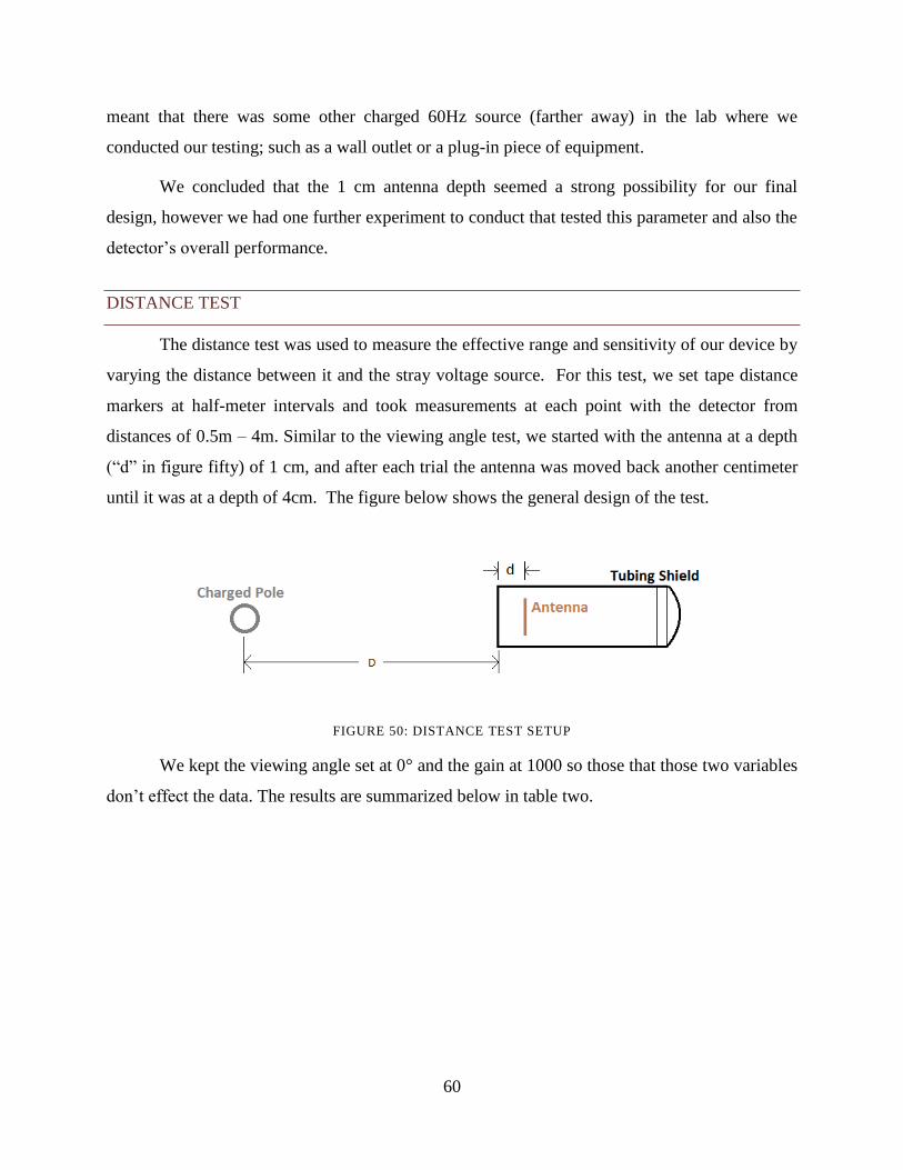
60
meant that there was some other charged 60Hz source (farther away) in the lab where we
conducted our testing; such as a wall outlet or a plug-in piece of equipment.
We concluded that the 1 cm antenna depth seemed a strong possibility for our final
design, however we had one further experiment to conduct that tested this parameter and also the
detector’s overall performance.
DISTANCE TEST
The distance test was used to measure the effective range and sensitivity of our device by
varying the distance between it and the stray voltage source. For this test, we set tape distance
markers at half-meter intervals and took measurements at each point with the detector from
distances of 0.5m – 4m. Similar to the viewing angle test, we started with the antenna at a depth
(“d” in figure fifty) of 1 cm, and after each trial the antenna was moved back another centimeter
until it was at a depth of 4cm. The figure below shows the general design of the test.
FIGURE 50: DISTANCE TEST SETUP
We kept the viewing angle set at 0° and the gain at 1000 so those that those two variables
don’t effect the data. The results are summarized below in table two.
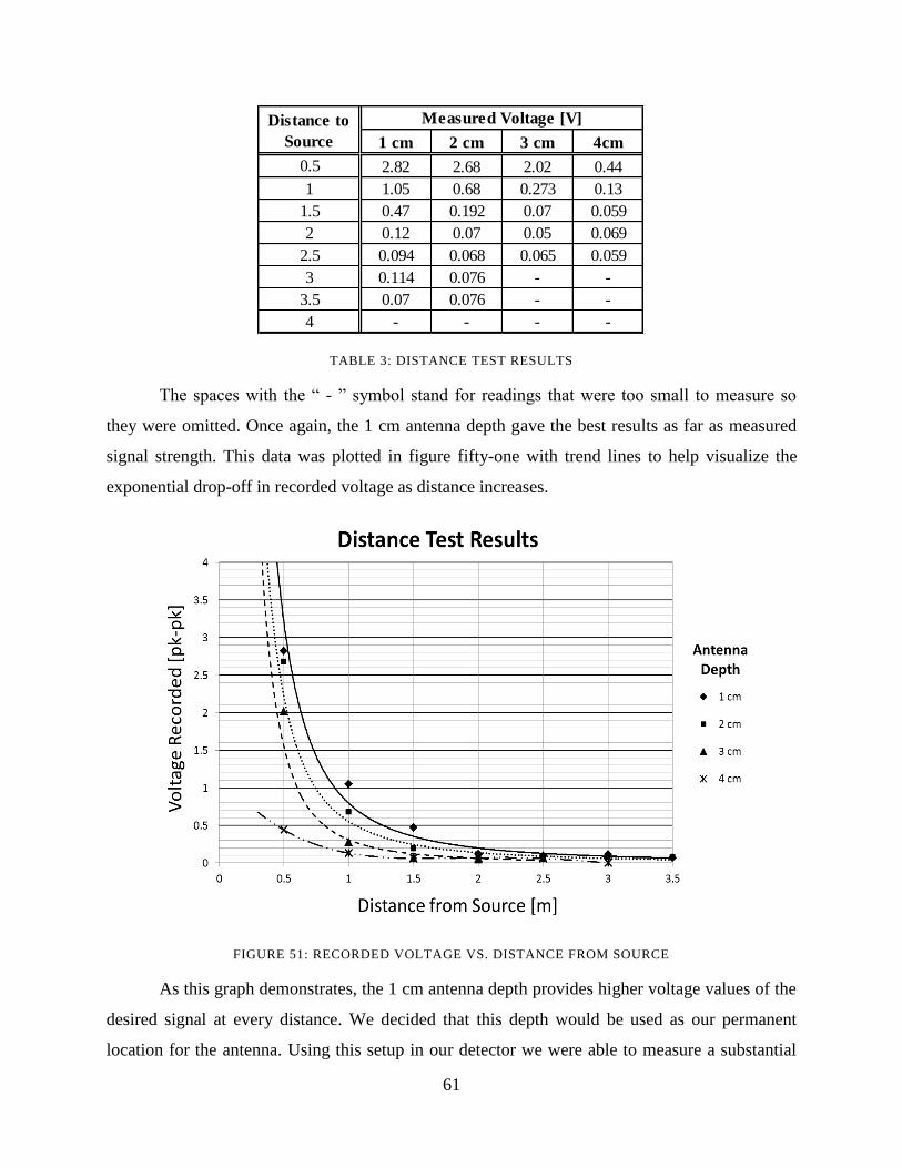
61
TABLE 3: DISTANCE TEST RESULTS
The spaces with the “ - ” symbol stand for readings that were too small to measure so
they were omitted. Once again, the 1 cm antenna depth gave the best results as far as measured
signal strength. This data was plotted in figure fifty-one with trend lines to help visualize the
exponential drop-off in recorded voltage as distance increases.
FIGURE 51: RECORDED VOLTAGE VS. DISTANCE FROM SOURCE
As this graph demonstrates, the 1 cm antenna depth provides higher voltage values of the
desired signal at every distance. We decided that this depth would be used as our permanent
location for the antenna. Using this setup in our detector we were able to measure a substantial
1 cm 2 cm 3 cm 4cm
0.5 2.82 2.68 2.02 0.44
1 1.05 0.68 0.273 0.13
1.5 0.47 0.192 0.07 0.059
2 0.12 0.07 0.05 0.069
2.5 0.094 0.068 0.065 0.059
3 0.114 0.076 - -
3.5 0.07 0.076 - -
4 - - - -
Distance to
Source
Measured Voltage [V]

62
voltage value (70 mV) at 3.5 meters away from the charged source. This was a great result
because it meant that we had successfully reached our goal: to design an easily portable and
handheld device that could detect voltages from at least two meters away.
RECOMMENDATIONS
Although our product is working as designed and detecting stray voltage sources, there
are a few things that we wish we had done somewhat differently. Due to time constraints we
were unable to make this prototype exactly how we wanted.
To future projects (if applicable) we would suggest adding or modifying only a few
things. The potentiometer tuning prior to any use of the device was quite annoying because of
the shield piping. We suggest that the next group design an ‘auto-zeroing’ circuit that would
make this problem a self-correcting issue. This way, the user could literally point and detect any
item without about worrying if the DC offset level is affecting the output measurements.
Another suggestion to future groups would be to include the digital processing stages
inside the piping so that the entire detector’s circuitry (filter, amplifier, and output logic) would
be shielded. This product could be used to detect different frequency levels by simply altering
the filter design to target that frequency range.
Finally, some other ideas that might make this product more user-friendly include the
addition of an auditory signal generator. The user could possibly wear headphones which plays a
beeping sound that increases in frequency the closer you get to a charged source.
CONCLUSION
This project is deemed a success because all proposed goals were met. The device was
successfully functional with an analog processing circuit driven by a single supply battery
source, implemented a grounding shield to prevent parasitic sources from influencing the voltage
measured at the antenna, and utilized a band-pass filter to only pass signals through that were
approximately 60 Hz (tolerance swayed usually by 2 Hz). The device successfully uses a button
trigger to conserve battery life, cylindrical tube housing to case all working circuitry, antenna,
and output wires to the oscilloscope or LED display. The device was successfully able to sense

63
stray voltage with accuracy from more than 3 meters away and performed greatest with an
antenna depth of 1 cm.
The LED display circuitry is still in the testing phase. As explained earlier, the LED can
only be illuminated one at a time from the decoder, so a small circuit using PNP transistors was
designed to create a waterfall effect. This effect will allow the top LED to illuminate and all
other lower LEDs will be turned on as well. Once testing is complete, it would be fitting to put
all circuitry within the cylindrical tube and mount the LED display for user interface.
As stated above, if this project were to be continued there are few recommendations for
the future project team. If the device had an “automatic Zero Offset Biasing” feature, it would
greatly improve the user interface because our design requires the operational amplifier to be
tuned manually to eliminate the offset bias. All circuitry should be incased in the same housing
as well. This will eliminate unwanted clutter the user will experience. Finally there should be an
audible sensor as well. This will increase user accuracy and reinforce what the visual sensor
already tells.
Overall, the device is a practical starting place for future project teams. With all the
foundations of a prototype down and all processing circuitry in order, the future project teams
would be able to design a device that is more practical for everyday use. Also improving the
performance of the amplifying circuit and equip it with an adjustable again stage to change the
sensitivity based on distance would be a viable addition. The device could also have a more
robust adjustable viewing angle slide to increase viewing angle accuracy as the object in question
is closer to the device. No matter what the following teams decide to do with the project, the
device designed and implemented in the last school year is a great beginning for any future
improvements because of its ability to sense a voltage from great distances with acceptable
sensitivity and directional sensitivity.
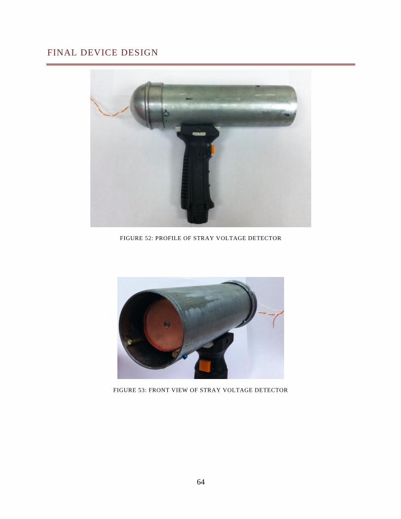
64
FINAL DEVICE DESIGN
FIGURE 52: PROFILE OF STRAY VOLTAGE DETECTOR
FIGURE 53: FRONT VIEW OF STRAY VOLTAGE DETECTOR

65
APPENDIX
CODE FOR ANALOG TO DIGITAL CONVERTER (MSP430)
#include <msp430g2231.h> #include <math.h> #define window 20 // 20 samples at about 10kHz is 0.05 seconds #define threshold1 0 // threshold energy #define threshold2 102 #define threshold3 204 #define threshold4 306 #define threshold5 408 #define threshold6 510 #define threshold7 612 #define threshold8 714 #define threshold9 816 #define threshold10 918 volatile long reading; int i=0; int average; // average value of the data array int pointer=0; // array pointer variable unsigned int data [window]; //array of window data void FaultRoutine(void); void ConfigClocks(void); void ConfigTimerA2(void); void ConfigADC10(void); void ConfigPins(void); void Warn(int); void main(void) WDTCTL = WDTPW + WDTHOLD; // Stop watchdog timer _BIS_SR(GIE); // Global Interrupt Enable ConfigPins(); // Configure the input and output pins ConfigClocks(); // Configure internal clocks ConfigTimerA2(); // Configure TimerA to interrupt at 10kHz ConfigADC10(); while(1) average=0; //initalize the energy to 0 for(i=0;i<window;i++) average= average +(data[i]); //add all the array elements together // end of main average=average/window; //average of the array to get one data output //if (data[0] > 800) // P1OUT |= BIT4; //else // P1OUT &= ~BIT4; Warn(average);

66
void FaultRoutine(void) P1OUT = 0x01; // red LED on while(1); // TRAP void ConfigClocks(void) if (CALBC1_1MHZ ==0xFF || CALDCO_1MHZ == 0xFF) FaultRoutine(); // If calibration data is erased // run FaultRoutine() BCSCTL1 = CALBC1_1MHZ; // Set range DCOCTL = CALDCO_1MHZ; // Set DCO step + modulation BCSCTL3 |= LFXT1S_0; // LFXT1 = cryatal32.768kHz IFG1 &= ~OFIFG; // Clear OSCFault flag BCSCTL2 |= SELM_0 + DIVM_0 + DIVS_0; // MCLK = DCO, SMCLK = DCO void ConfigADC10(void) ADC10CTL0 = SREF_0 + ADC10SHT_0 + ADC10ON + ADC10IE; // VCC and Vss ADC10CTL1 = INCH_5 + ADC10DIV_0; // A0 ADC10CLK ADC10AE0 = BIT5; void ConfigTimerA2(void) CCTL0 = CCIE; // interupt enable CCR0 = 10; // interrupt at 10kHz TACTL = TASSEL_1 + MC_1; // ACLK, operate in up mode void ConfigPins(void) P1DIR &= ~BIT5; //set P1.5 to be input P1SEL = BIT5; //set P1.5 to be ADC input P1DIR |= BIT1 + BIT2 + BIT3 +BIT4; //set P1.1-4 to be output to decoder P1OUT &=~BIT1 + ~BIT2 + ~BIT3 +~BIT4; //set P1.1-4 low void Warn(int averageADC) if (averageADC > threshold10) //setting thresholds Highest to lowest. P1OUT=BIT4 + BIT2; //Setting outputs to decoder else if (averageADC > threshold9) P1OUT= BIT4 + BIT1; else if (averageADC > threshold8) //the error would be only if the bit one is lit up. get rid of else and just if P1OUT= BIT4; else if (averageADC > threshold7) // then add breaks. P1OUT= BIT3 + BIT2 +BIT1; else if (averageADC > threshold6)

67
P1OUT= BIT3 + BIT2; else if (averageADC > threshold5) P1OUT= BIT3 + BIT1; else if (averageADC > threshold4) P1OUT= BIT3; else if (averageADC > threshold3) P1OUT= BIT2 + BIT1; else if (averageADC > threshold2) P1OUT= BIT2; else if (averageADC > threshold1) P1OUT= BIT1; #pragma vector=TIMERA0_VECTOR __interrupt void Timer_A (void) ADC10CTL0 |= ENC + ADC10SC; // Samp and convert start #pragma vector=ADC10_VECTOR __interrupt void ADC10 (void) reading = ADC10MEM; // Read conversion value data[pointer]=reading; // transfer reading to the array pointer++; //increment pointer variable pointer=pointer%window; //loop through the array and replace oldest value

68
REFERENCES
[1.] Burke, J. (2007). The Confusion Surrounding "Stray Voltage". Rapid City, SD: IEEE.
[2.] Bierbaum, A. C. (1992). Diagnosis and Trouble Shooting of Stray Voltage Problems. New
Orleans, LA: IEEE.
[3.] Williams, C. (2006). Was the Stray Voltage Really Stray? Dallas, TX: IEEE.
[4.] http://caselaw.findlaw.com/wa-court-of-appeals/1323678.html
[5.] http://www.mba.state.mn.us/resource.html?Id=17470
[6.] http://www.santafenewmexican.com/Local%20News/Shocker--Lamppost-short-circuits-pets
[7.] http://www.nytimes.com/2006/03/04/nyregion/04voltage.html?_r=2
[8.] http://cityroom.blogs.nytimes.com/2008/01/18/stray-voltage-still-a-problem-4-years-later/
[9.] http://www.google.com/patents?id=66ClAAAAEBAJ&printsec=abstract&zoom=4#v=on
epage&q&f=false
[10.]
http://www.google.com/patents?id=m6URAAAAEBAJ&pg=PA15&dq=ac+voltage+detector
+handheld&hl=en&ei=e7NvT4WpCerf0QHHhvDOBg&sa=X&oi=book_result&ct=book
-thumbnail&resnum=4&ved=0CDwQ6wEwAw#v=onepage&q=ac%20voltage
%20detector%20handheld&f=false
[11.]
http://www.google.com/patents?id=l1J4AAAAEBAJ&pg=PA9&dq=high+voltage+detector&
hl=en&sa=X&ei=94dwT--_I-Pz0gHkrYzSBg&sqi=2&ved=0CDgQ6AEwAg#v
=onepage&q=high%20voltage%20detector&f=true