Embed Size (px)
Citation preview
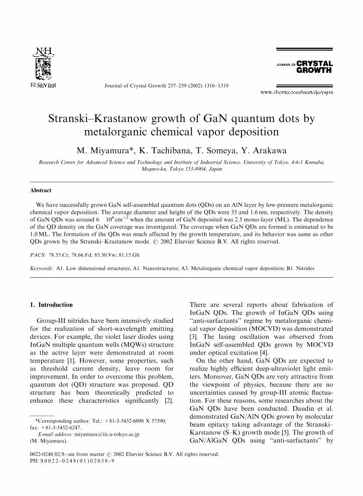
Journal of Crystal Growth 237–239 (2002) 1316–1319
Stranski–Krastanow growth of GaN quantum dots bymetalorganic chemical vapor deposition
M. Miyamura*, K. Tachibana, T. Someya, Y. Arakawa
Research Center for Advanced Science and Technology and Institute of Industrial Science, University of Tokyo, 4-6-1 Komaba,
Meguro-ku, Tokyo 153-8904, Japan
Abstract
We have successfully grown GaN self-assembled quantum dots (QDs) on an AlN layer by low-pressure metalorganic
chemical vapor deposition. The average diameter and height of the QDs were 35 and 1.6 nm, respectively. The density
of GaN QDs was around 6� 108 cm�2 when the amount of GaN deposited was 2.5 mono-layer (ML). The dependence
of the QD density on the GaN coverage was investigated. The coverage when GaN QDs are formed is estimated to be
1.0ML. The formation of the QDs was much affected by the growth temperature, and its behavior was same as other
QDs grown by the Stranski–Krastanow mode. r 2002 Elsevier Science B.V. All rights reserved.
PACS: 78.55.Cr; 78.66.Fd; 85.30.Vw; 81.15.Gh
Keywords: A1. Low dimensional structures; A1. Nanostructures; A3. Metalorganic chemical vapor deposition; B1. Nitrides
1. Introduction
Group-III nitrides have been intensively studiedfor the realization of short-wavelength emittingdevices. For example, the violet laser diodes usingInGaN multiple quantum wells (MQWs) structureas the active layer were demonstrated at roomtemperature [1]. However, some properties, suchas threshold current density, leave room forimprovement. In order to overcome this problem,quantum dot (QD) structure was proposed. QDstructure has been theoretically predicted toenhance these characteristics significantly [2].
There are several reports about fabrication ofInGaN QDs. The growth of InGaN QDs using‘‘anti-surfactants’’ regime by metalorganic chemi-cal vapor deposition (MOCVD) was demonstrated[3]. The lasing oscillation was observed fromInGaN self-assembled QDs grown by MOCVDunder optical excitation [4].On the other hand, GaN QDs are expected to
realize highly efficient deep-ultraviolet light emit-ters. Moreover, GaN QDs are very attractive fromthe viewpoint of physics, because there are nouncertainties caused by group-III atomic fluctua-tion. For these reasons, some researches about theGaN QDs have been conducted. Daudin et al.demonstrated GaN/AlN QDs grown by molecularbeam epitaxy taking advantage of the Stranski–Karstanow (S–K) growth mode [5]. The growth ofGaN/AlGaN QDs using ‘‘anti-surfactants’’ by
*Corresponding author. Tel.: +81-3-5452-6098 X 57590;
fax: +81-3-5452-6247.
E-mail address: [email protected]
(M. Miyamura).
0022-0248/02/$ - see front matter r 2002 Elsevier Science B.V. All rights reserved.
PII: S 0 0 2 2 - 0 2 4 8 ( 0 1 ) 0 2 0 5 8 - 9
MOCVD and stimulation of emission from theseQDs were also reported [6,7]. As another way tofabricate GaN or InGaN QDs, the selectivegrowth method was proposed [8]. But there areno reports on the self-assembled growth of GaNQDs without any ‘‘anti-surfactants’’ by MOCVD.In this paper, we demonstrate the GaN self-
assembled QDs grown on a very flat surface ofAlN by low-pressure MOCVD. The formation ofGaN QDs is explained mainly by the 2.5% latticemismatch of the GaN/AlN system. First, thegrowth conditions of an AlN buffer layer andGaN QDs are introduced. This AlN layer ischaracterized by X-ray diffraction (XRD) andatomic force microscopy (AFM) measurements.We investigated the dependence of the QD densityon the GaN coverage. Finally, the influence of thegrowth temperature on the formation of GaNQDs is discussed.
2. Experimental procedure
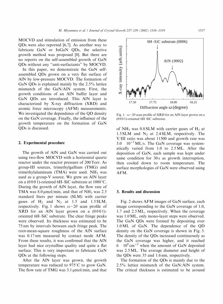
The growth of AlN and GaN was carried outusing two-flow MOCVD with a horizontal quartzreactor under the reactor pressure of 200Torr. Asgroup-III sources, trimethylgallium (TMG) andtrimethylaluminum (TMA) were used. NH3 wasused as a group-V source. We grew an AlN layeron a (0 0 0 1)-oriented 6H–SiC substrate at 10801C.During the growth of AlN layer, the flow rate ofTMA was 8.0 mmol/min, and that of NH3 was 2.5standard liters per minute (SLM) with carriergases of H2 and N2 at 1.5 and 1.5 SLM,respectively. Fig. 1 shows o22y scan profile ofXRD for an AlN layer grown on a (0 0 0 1)-oriented 6H–SiC substrate. The clear fringe peakswere observed. Its thickness was estimated to be75 nm by intervals between each fringe peak. Theroot-mean-square roughness of the AlN surfacewas 0.17 nm measured by contact mode AFM.From these results, it was confirmed that the AlNlayer had nice crystalline quality and quite a flatsurface. This is very important to fabricate GaNQDs at the following steps.After the AlN layer was grown, the growth
temperature was reduced to 9751C to grow GaN.The flow rate of TMG was 3.1 mmol/min, and that
of NH3 was 0.8 SLM with carrier gases of H2 at1.5 SLM and N2 at 2.4 SLM, respectively. TheV/III ratio was about 11500 and growth rate was5.0� 10�2ML/s. The GaN coverage was system-atically varied from 1.0 to 2.5ML. After thedeposition of GaN, each sample was kept undersame condition for 30 s as growth interruption,then cooled down to room temperature. Thesurface morphologies of GaN were observed usingAFM.
3. Results and discussion
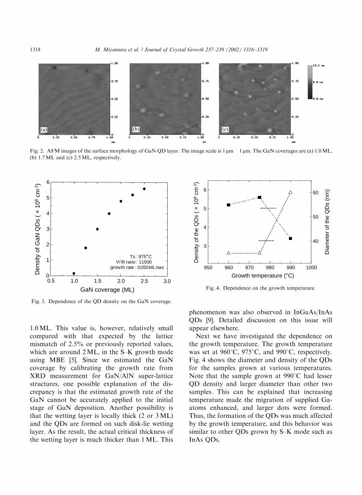
Fig. 2 shows AFM images of GaN surface, eachimage corresponding to the GaN coverage of 1.0,1.7 and 2.5ML, respectively. When the coveragewas 1.0ML, only mono-layer steps were observed.The GaN QDs were formed by depositing over1.0ML of GaN. The dependence of the QDdensity on the GaN coverage is shown in Fig. 3.The density of the QDs increased continuously asthe GaN coverage was higher, and it reached6� 108 cm�2 when the amount of GaN depositedwas 2.5ML. The average diameter and height ofthe QDs were 35 and 1.6 nm, respectively.The formation of the QDs is mainly due to the
2.5% lattice mismatch of the GaN/AlN system.The critical thickness is estimated to be around
17.50 17.75 18.00 18.25
AlN (0002)
6H -SiC substrate (0006)
X-r
ay i
nten
sity
(ar
b.un
its)
Diffraction angle ω (degree)
Fig. 1. o22y scan profile of XRD for an AlN layer grown on a
(0 0 0 1)-oriented 6H–SiC substrate.
M. Miyamura et al. / Journal of Crystal Growth 237–239 (2002) 1316–1319 1317
1.0ML. This value is, however, relatively smallcompared with that expected by the latticemismatch of 2.5% or previously reported values,which are around 2ML, in the S–K growth modeusing MBE [5]. Since we estimated the GaNcoverage by calibrating the growth rate fromXRD measurement for GaN/AlN super-latticestructures, one possible explanation of the dis-crepancy is that the estimated growth rate of theGaN cannot be accurately applied to the initialstage of GaN deposition. Another possibility isthat the wetting layer is locally thick (2 or 3ML)and the QDs are formed on such disk-lie wettinglayer. As the result, the actual critical thickness ofthe wetting layer is much thicker than 1ML. This
phenomenon was also observed in InGaAs/InAsQDs [9]. Detailed discussion on this issue willappear elsewhere.Next we have investigated the dependence on
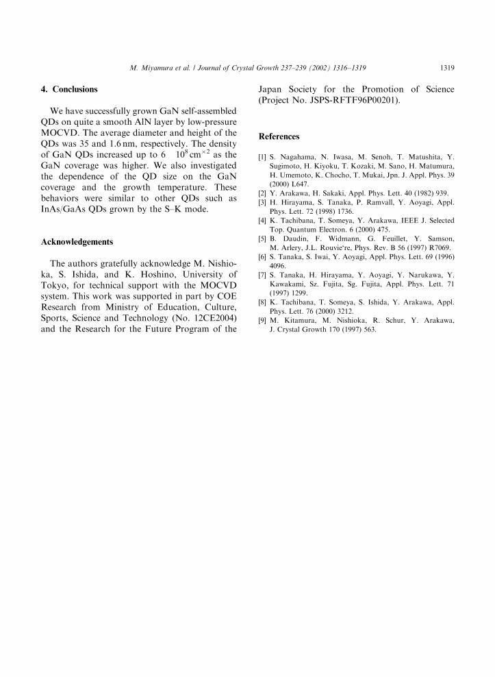
the growth temperature. The growth temperaturewas set at 9601C, 9751C, and 9901C, respectively.Fig. 4 shows the diameter and density of the QDsfor the samples grown at various temperatures.Note that the sample grown at 9901C had lesserQD density and larger diameter than other twosamples. This can be explained that increasingtemperature made the migration of supplied Ga-atoms enhanced, and larger dots were formed.Thus, the formation of the QDs was much affectedby the growth temperature, and this behavior wassimilar to other QDs grown by S–K mode such asInAs QDs.
0.5 1.0 1.5 2.0 2.5 3.00
1
2
3
4
5
6
Ts : 975˚CV/ III ratio : 11500
growth rate : 0.050 ML/sec
Den
sity
of G
aN Q
Ds
( ×
108
cm
-2)
GaN coverage (ML)
Fig. 3. Dependence of the QD density on the GaN coverage.
950 960 970 980 990 1000
3
4
5
6D
ensi
ty o
f the
QD
s (
× 1
08 c
m-2
)
Growth temperature (˚C)
40
50
60
Dia
met
er o
f the
QD
s (n
m)
Fig. 4. Dependence on the growth temperature.
Fig. 2. AFM images of the surface morphology of GaN QD layer. The image scale is 1 mm� 1mm. The GaN coverages are (a) 1.0ML,
(b) 1.7ML and (c) 2.5ML, respectively.
M. Miyamura et al. / Journal of Crystal Growth 237–239 (2002) 1316–13191318
4. Conclusions
We have successfully grown GaN self-assembledQDs on quite a smooth AlN layer by low-pressureMOCVD. The average diameter and height of theQDs was 35 and 1.6 nm, respectively. The densityof GaN QDs increased up to 6� 108 cm�2 as theGaN coverage was higher. We also investigatedthe dependence of the QD size on the GaNcoverage and the growth temperature. Thesebehaviors were similar to other QDs such asInAs/GaAs QDs grown by the S–K mode.
Acknowledgements
The authors gratefully acknowledge M. Nishio-ka, S. Ishida, and K. Hoshino, University ofTokyo, for technical support with the MOCVDsystem. This work was supported in part by COEResearch from Ministry of Education, Culture,Sports, Science and Technology (No. 12CE2004)and the Research for the Future Program of the
Japan Society for the Promotion of Science(Project No. JSPS-RFTF96P00201).
References
[1] S. Nagahama, N. Iwasa, M. Senoh, T. Matushita, Y.
Sugimoto, H. Kiyoku, T. Kozaki, M. Sano, H. Matumura,
H. Umemoto, K. Chocho, T. Mukai, Jpn. J. Appl. Phys. 39
(2000) L647.
[2] Y. Arakawa, H. Sakaki, Appl. Phys. Lett. 40 (1982) 939.
[3] H. Hirayama, S. Tanaka, P. Ramvall, Y. Aoyagi, Appl.
Phys. Lett. 72 (1998) 1736.
[4] K. Tachibana, T. Someya, Y. Arakawa, IEEE J. Selected
Top. Quantum Electron. 6 (2000) 475.
[5] B. Daudin, F. Widmann, G. Feuillet, Y. Samson,
M. Arlery, J.L. Rouvie‘re, Phys. Rev. B 56 (1997) R7069.
[6] S. Tanaka, S. Iwai, Y. Aoyagi, Appl. Phys. Lett. 69 (1996)
4096.
[7] S. Tanaka, H. Hirayama, Y. Aoyagi, Y. Narukawa, Y.
Kawakami, Sz. Fujita, Sg. Fujita, Appl. Phys. Lett. 71
(1997) 1299.
[8] K. Tachibana, T. Someya, S. Ishida, Y. Arakawa, Appl.
Phys. Lett. 76 (2000) 3212.
[9] M. Kitamura, M. Nishioka, R. Schur, Y. Arakawa,
J. Crystal Growth 170 (1997) 563.
M. Miyamura et al. / Journal of Crystal Growth 237–239 (2002) 1316–1319 1319