Embed Size (px)
Citation preview
Strain-Balanced Quantum Well Solar Cells From Multi-Wafer Production
Jessica Adams
33rd IEEE Photovoltaic Specialists Conference
12th May 2008

Can we manufacture the strain-balanced quantum well solar cell on a multi-wafer
production run?
Research wafers Industrial wafers
2”
4”
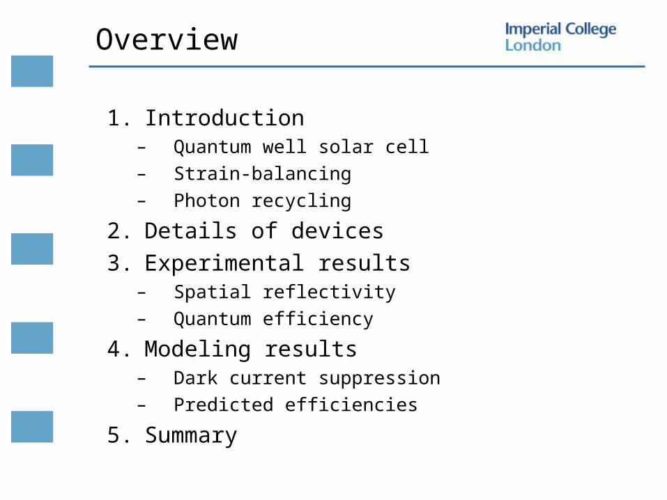
1. Introduction
– Quantum well solar cell– Strain-balancing– Photon recycling
2. Details of devices
3. Experimental results– Spatial reflectivity– Quantum efficiency
4. Modeling results– Dark current suppression– Predicted efficiencies
5. Summary
Overview

Strain-Balanced Quantum Well Solar Cell (I)
• Wells inserted in i-region of p-i-n
• Extends absorption energy range to below that of bulk
p i n
Ea
Eg
V
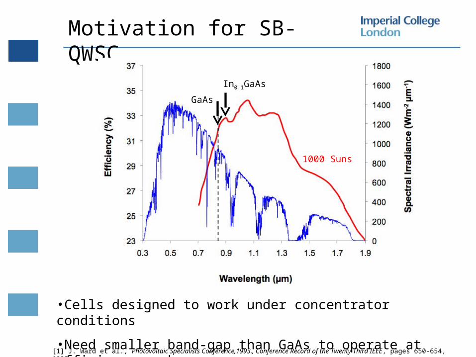
Motivation for SB-QWSC
[1] J. Ward et al., Photovoltaic Specialists Conference,1993., Conference Record of the Twenty Third IEEE, pages 650-654, 1993.
•Cells designed to work under concentrator conditions
•Need smaller band-gap than GaAs to operate at efficiency peak
GaAs
In0.1GaAs
1000 Suns
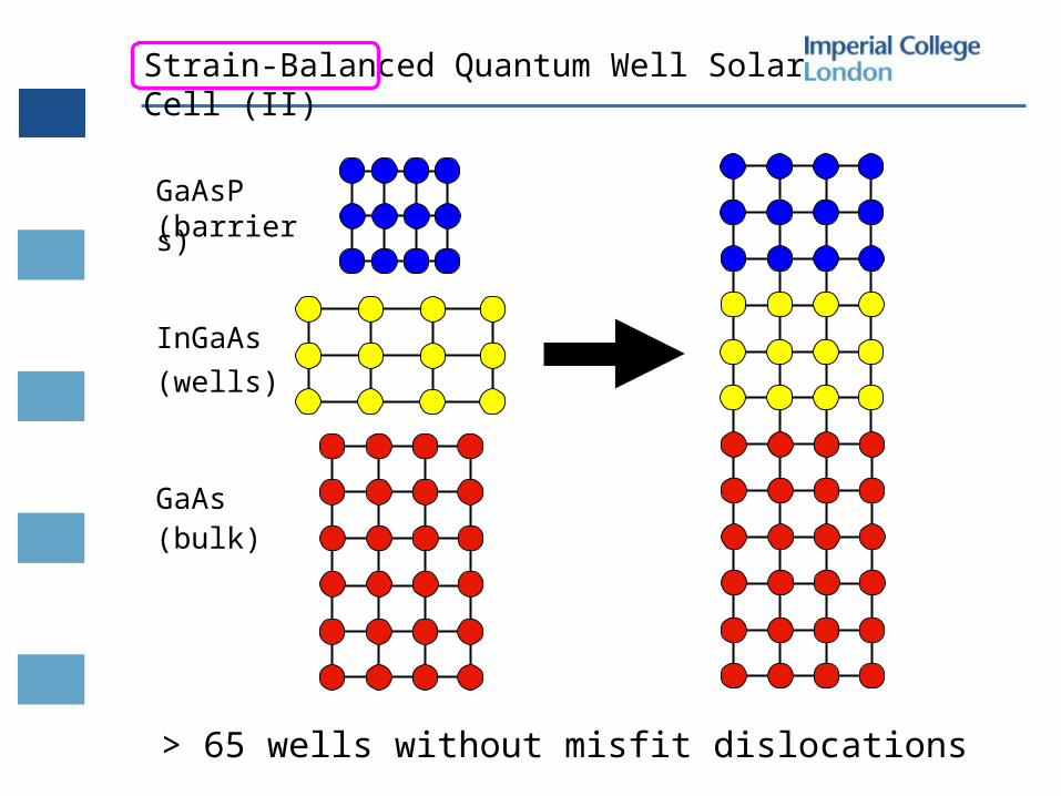
GaAsP(barriers)
InGaAs
(wells)
GaAs(bulk)
> 65 wells without misfit dislocations
Strain-Balanced Quantum Well Solar Cell (II)

• Photons not absorbed on first pass reflected => increased JSC
• Photons from radiative recombination loss reflected back through wells => photon recycling => increased VOC
• Efficiency increased ~1 % absolute
Photon Recycling
Quantum wells
Distributed Bragg reflector (mirror)
n
p
ContactAR coat
i
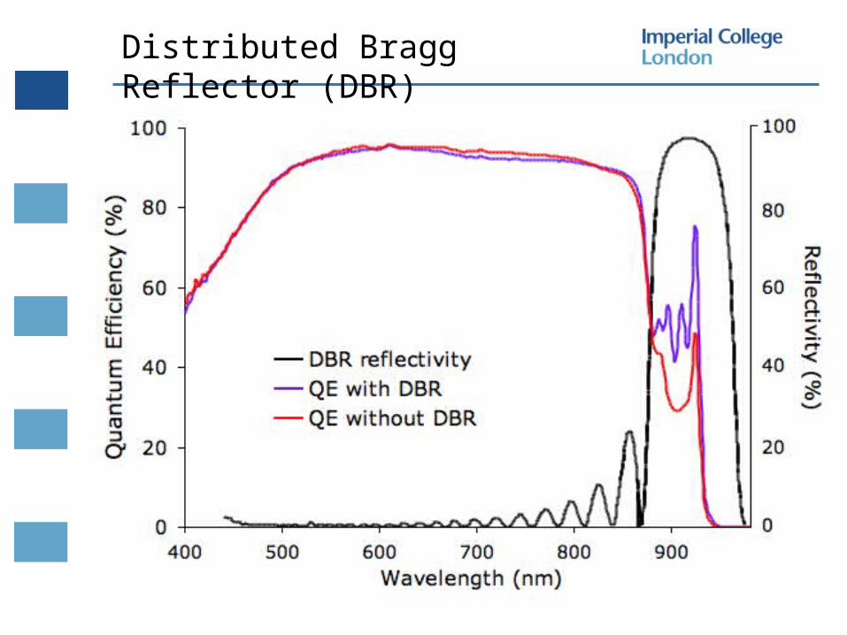
Distributed Bragg Reflector (DBR)
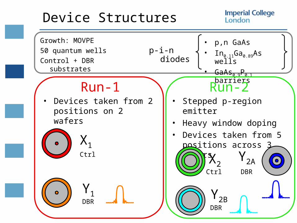
Device Structures
Growth: MOVPE
50 quantum wells
Control + DBR substrates
p-i-n diodes• p,n GaAs• In0.11Ga0.89As wells• GaAs0.9P0.1 barriers
• Devices taken from 2 positions on 2 wafers
Run-1 Run-2• Stepped p-region emitter• Heavy window doping• Devices taken from 5
positions across 3 wafersX1
Y1
Ctrl
DBR
X2
Y2B
Ctrl
DBR
DBR
Y2A

DBR Spatial Reflectivity
Wavelength of maximum reflectivity varies from 924 nm to 904 nm
X1
X1
Y1
Y1
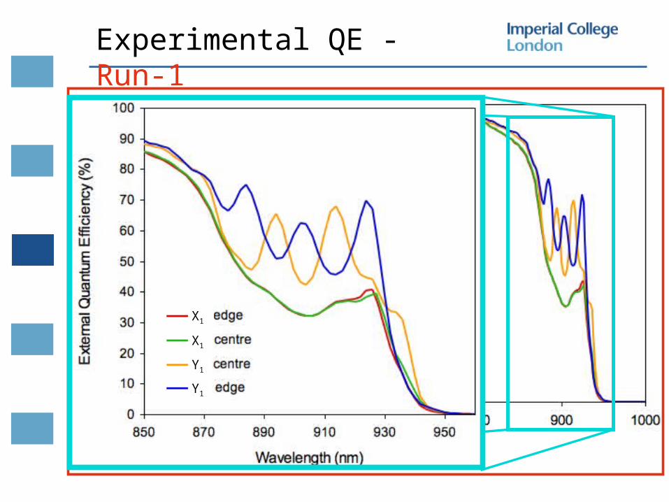
Experimental QE - Run-1
X1
X1
Y1
Y1

Y2A
Y2A
Y2B
X2
X2
X2
X2
Y2B
Y2A
Y2A
Experimental QE - Run-2
Carrier transport
Quantum well absorption
Carrier distributions
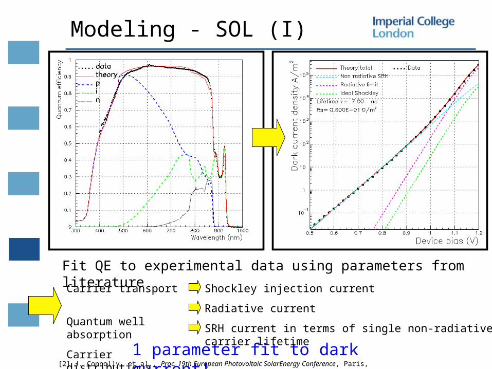
Modeling - SOL (I)
Fit QE to experimental data using parameters from literature
1 parameter fit to dark current!
Shockley injection current
Radiative current
SRH current in terms of single non-radiative carrier lifetime
[2] J. Connolly, et al., Proc. 19th European Photovoltaic SolarEnergy Conference, Paris, 2004.
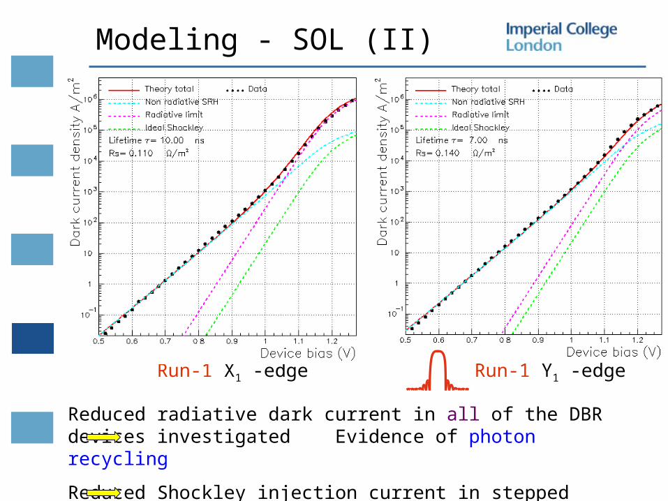
Modeling - SOL (II)
Run-1 X1 -edge Run-1 Y1 -edge
Reduced radiative dark current in all of the DBR devices investigated Evidence of photon recycling
Reduced Shockley injection current in stepped emitter devicesEvidence of reduced surface recombination current

Predicted Efficiencies
X1
Y1
AM1.5D x500
5% shading
Run-1
X2
Y2A
Y2B
Run-2
Effi
cie
ncy
(%
)
25.5
28.0
27.5
26.0
27.0
26.5
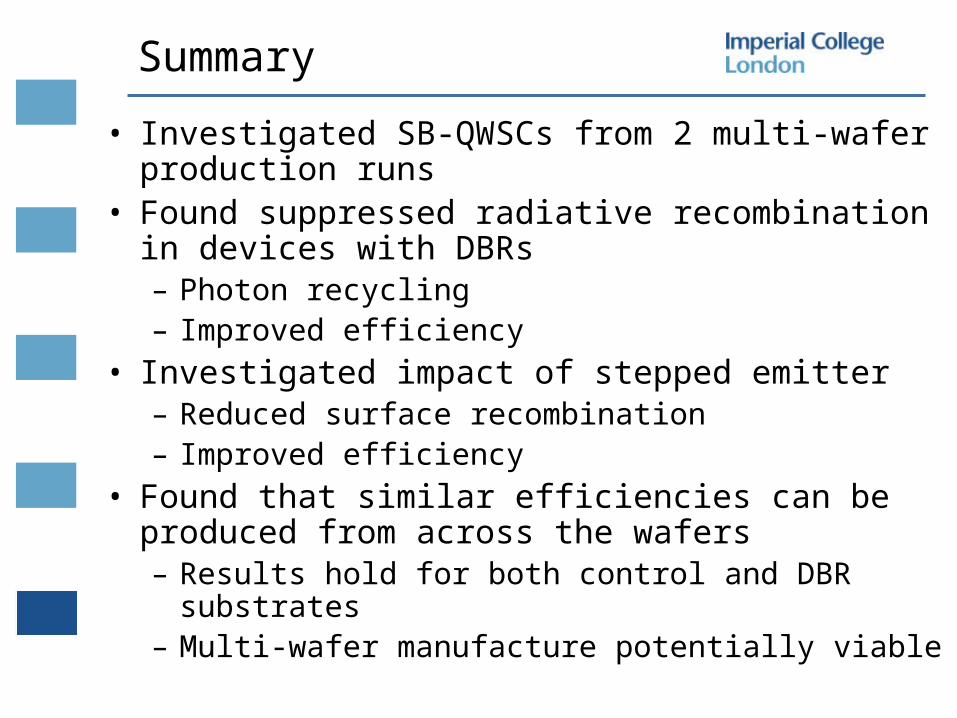
• Investigated SB-QWSCs from 2 multi-wafer production runs
• Found suppressed radiative recombination in devices with DBRs– Photon recycling– Improved efficiency
• Investigated impact of stepped emitter– Reduced surface recombination– Improved efficiency
• Found that similar efficiencies can be produced from across the wafers– Results hold for both control and DBR substrates– Multi-wafer manufacture potentially viable
Summary
Keith Barnham, James Connolly and the QPV group at Imperial College London
J.S. Roberts and G. Hill at the EPSRC National Centre for III-V Technologies
T. Tibbits of QuantaSol Ltd.
M. Geen of IQE Europe
M. Pate of the Centre for Integrated Photonics
Acknowledgments
http://www.sc.ic.ac.uk/~q_pv


![Mechanical Load Testing of Solar Panels – Beyond ...brightspotautomation.com/wp-content/uploads/2020/... · [Beck, Siva, NREL PVMRW 2016] 9 43RD IEEE PHOTOVOLTAIC SPECIALISTS CONFERENCE](https://img.pdfslide.us/doc/110x75/600bd4b3e9436f129f30f4c0/mechanical-load-testing-of-solar-panels-a-beyond-beck-siva-nrel-pvmrw-2016.jpg)


![ACES-Cosim: A Framework to Simulate Advanced Electric … · 2020. 3. 3. · Robert Broderick, Photovoltaic Specialists Conference, 2017 [3]Presentation: “ARPA-E Energy Summit in](https://img.pdfslide.us/doc/110x75/603812daeedcab35a766ae84/aces-cosim-a-framework-to-simulate-advanced-electric-2020-3-3-robert-broderick.jpg)