Embed Size (px)
Citation preview
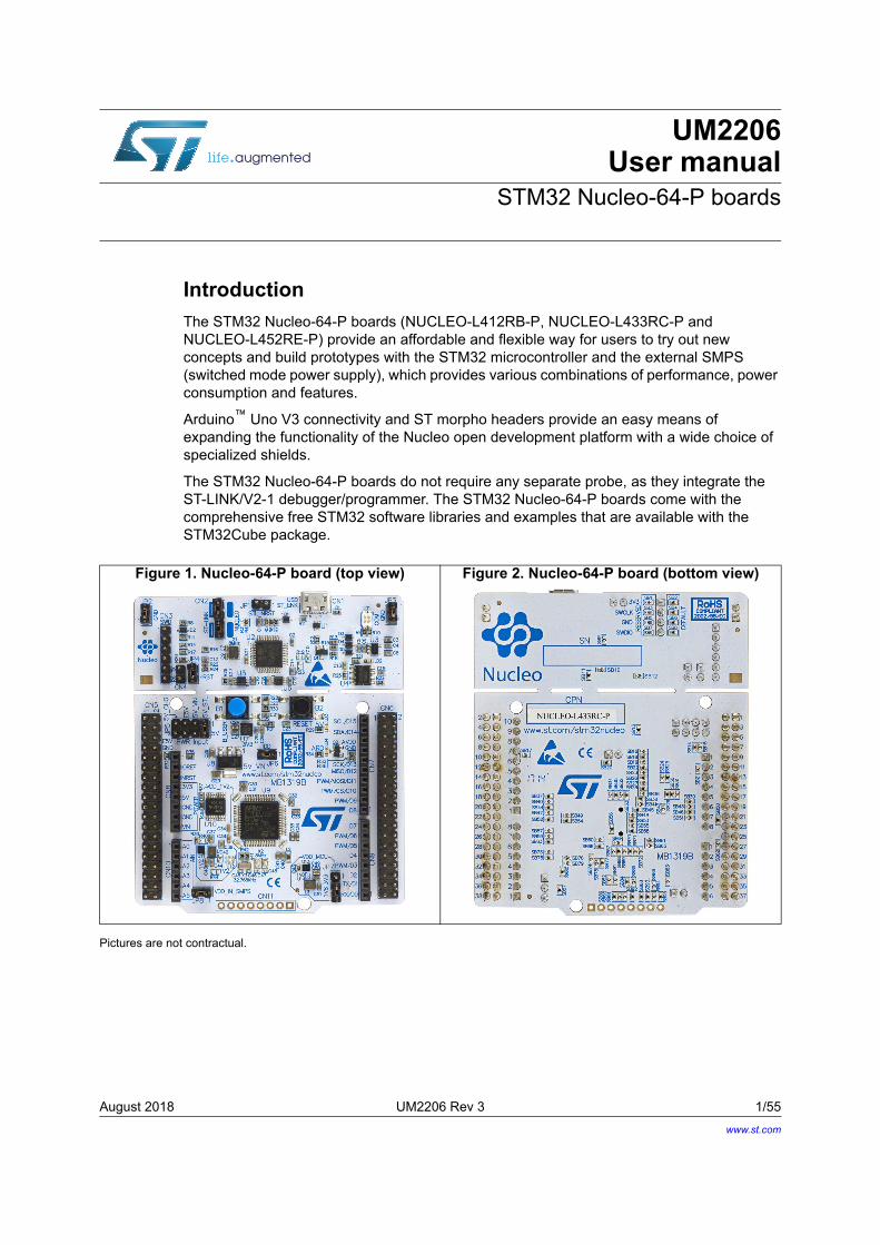
August 2018 UM2206 Rev 3 1/55
1
UM2206User manual
STM32 Nucleo-64-P boards
Introduction
The STM32 Nucleo-64-P boards (NUCLEO-L412RB-P, NUCLEO-L433RC-P and NUCLEO-L452RE-P) provide an affordable and flexible way for users to try out new concepts and build prototypes with the STM32 microcontroller and the external SMPS (switched mode power supply), which provides various combinations of performance, power consumption and features.
Arduino™ Uno V3 connectivity and ST morpho headers provide an easy means of expanding the functionality of the Nucleo open development platform with a wide choice of specialized shields.
The STM32 Nucleo-64-P boards do not require any separate probe, as they integrate the ST-LINK/V2-1 debugger/programmer. The STM32 Nucleo-64-P boards come with the comprehensive free STM32 software libraries and examples that are available with the STM32Cube package.
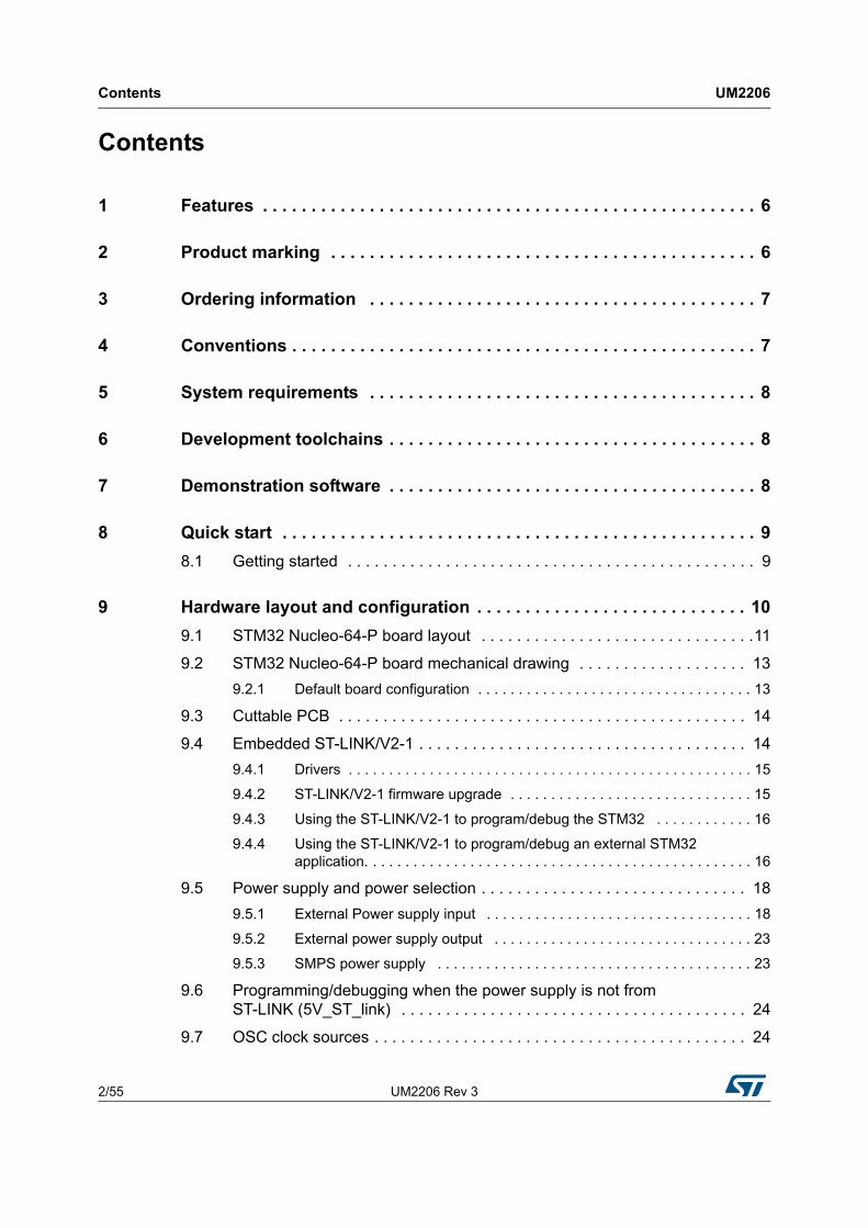
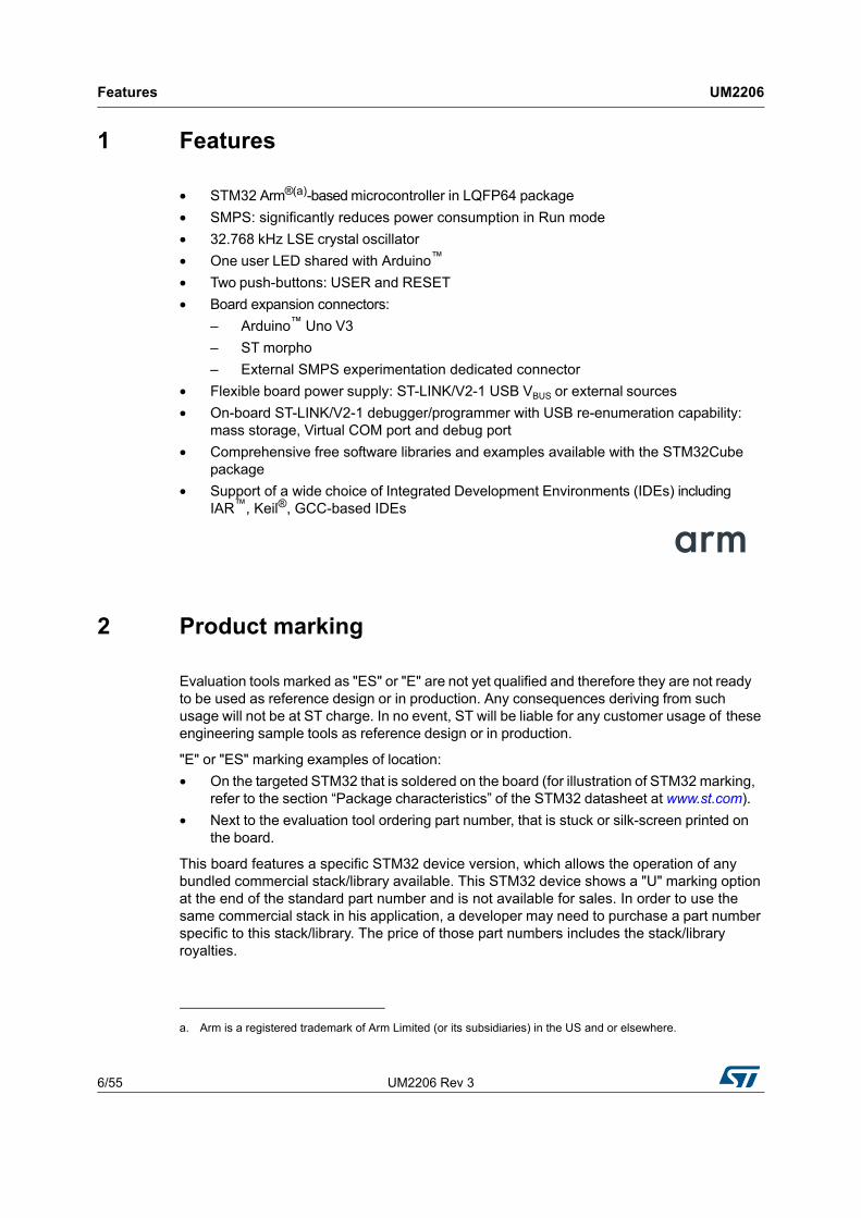
Pictures are not contractual.
Figure 1. Nucleo-64-P board (top view) Figure 2. Nucleo-64-P board (bottom view)
www.st.com
Contents UM2206
2/55 UM2206 Rev 3
Contents
1 Features . . . . . . . . . . . . . . . . . . . . . . . . . . . . . . . . . . . . . . . . . . . . . . . . . . . 6
2 Product marking . . . . . . . . . . . . . . . . . . . . . . . . . . . . . . . . . . . . . . . . . . . . 6
3 Ordering information . . . . . . . . . . . . . . . . . . . . . . . . . . . . . . . . . . . . . . . . 7
4 Conventions . . . . . . . . . . . . . . . . . . . . . . . . . . . . . . . . . . . . . . . . . . . . . . . . 7
5 System requirements . . . . . . . . . . . . . . . . . . . . . . . . . . . . . . . . . . . . . . . . 8
6 Development toolchains . . . . . . . . . . . . . . . . . . . . . . . . . . . . . . . . . . . . . . 8
7 Demonstration software . . . . . . . . . . . . . . . . . . . . . . . . . . . . . . . . . . . . . . 8
8 Quick start . . . . . . . . . . . . . . . . . . . . . . . . . . . . . . . . . . . . . . . . . . . . . . . . . 9
8.1 Getting started . . . . . . . . . . . . . . . . . . . . . . . . . . . . . . . . . . . . . . . . . . . . . . 9
9 Hardware layout and configuration . . . . . . . . . . . . . . . . . . . . . . . . . . . . 10
9.1 STM32 Nucleo-64-P board layout . . . . . . . . . . . . . . . . . . . . . . . . . . . . . . .11
9.2 STM32 Nucleo-64-P board mechanical drawing . . . . . . . . . . . . . . . . . . . 13
9.2.1 Default board configuration . . . . . . . . . . . . . . . . . . . . . . . . . . . . . . . . . . 13
9.3 Cuttable PCB . . . . . . . . . . . . . . . . . . . . . . . . . . . . . . . . . . . . . . . . . . . . . . 14
9.4 Embedded ST-LINK/V2-1 . . . . . . . . . . . . . . . . . . . . . . . . . . . . . . . . . . . . . 14
9.4.1 Drivers . . . . . . . . . . . . . . . . . . . . . . . . . . . . . . . . . . . . . . . . . . . . . . . . . . 15
9.4.2 ST-LINK/V2-1 firmware upgrade . . . . . . . . . . . . . . . . . . . . . . . . . . . . . . 15
9.4.3 Using the ST-LINK/V2-1 to program/debug the STM32 . . . . . . . . . . . . 16
9.4.4 Using the ST-LINK/V2-1 to program/debug an external STM32 application. . . . . . . . . . . . . . . . . . . . . . . . . . . . . . . . . . . . . . . . . . . . . . . . 16
9.5 Power supply and power selection . . . . . . . . . . . . . . . . . . . . . . . . . . . . . . 18
9.5.1 External Power supply input . . . . . . . . . . . . . . . . . . . . . . . . . . . . . . . . . 18
9.5.2 External power supply output . . . . . . . . . . . . . . . . . . . . . . . . . . . . . . . . 23
9.5.3 SMPS power supply . . . . . . . . . . . . . . . . . . . . . . . . . . . . . . . . . . . . . . . 23
9.6 Programming/debugging when the power supply is not from ST-LINK (5V_ST_link) . . . . . . . . . . . . . . . . . . . . . . . . . . . . . . . . . . . . . . . 24
9.7 OSC clock sources . . . . . . . . . . . . . . . . . . . . . . . . . . . . . . . . . . . . . . . . . . 24
UM2206 Rev 3 3/55
UM2206 Contents
3
9.7.1 LSE: OSC 32 KHz clock supply . . . . . . . . . . . . . . . . . . . . . . . . . . . . . . . 24
9.7.2 OSC clock supply . . . . . . . . . . . . . . . . . . . . . . . . . . . . . . . . . . . . . . . . . 25
9.8 Reset sources . . . . . . . . . . . . . . . . . . . . . . . . . . . . . . . . . . . . . . . . . . . . . 26
9.9 Virtual COM port: LPUART1/USART1 . . . . . . . . . . . . . . . . . . . . . . . . . . . 26
9.10 LEDs . . . . . . . . . . . . . . . . . . . . . . . . . . . . . . . . . . . . . . . . . . . . . . . . . . . . 26
9.11 Push buttons . . . . . . . . . . . . . . . . . . . . . . . . . . . . . . . . . . . . . . . . . . . . . . 27
9.12 IDD measurement . . . . . . . . . . . . . . . . . . . . . . . . . . . . . . . . . . . . . . . . . . 27
9.13 Jumper configuration . . . . . . . . . . . . . . . . . . . . . . . . . . . . . . . . . . . . . . . . 28
9.14 Configuration of the solder bridges . . . . . . . . . . . . . . . . . . . . . . . . . . . . . 28
10 Connectors . . . . . . . . . . . . . . . . . . . . . . . . . . . . . . . . . . . . . . . . . . . . . . . 33
10.1 USB Micro-B connector CN1 . . . . . . . . . . . . . . . . . . . . . . . . . . . . . . . . . . 33
10.2 Arduino Uno V3 connectors . . . . . . . . . . . . . . . . . . . . . . . . . . . . . . . . . . . 34
10.3 ST morpho connectors CN5 and CN6 . . . . . . . . . . . . . . . . . . . . . . . . . . . 37
10.4 External power connector . . . . . . . . . . . . . . . . . . . . . . . . . . . . . . . . . . . . . 38
Appendix A NUCLEO-L412RB-P, NUCLEO-L433RC-P and NUCLEO-L452RE-P I/O assignment . . . . . . . . . . . . . . . . . . . . . . . . . . . . . . . . . . . . . . . . . . 40
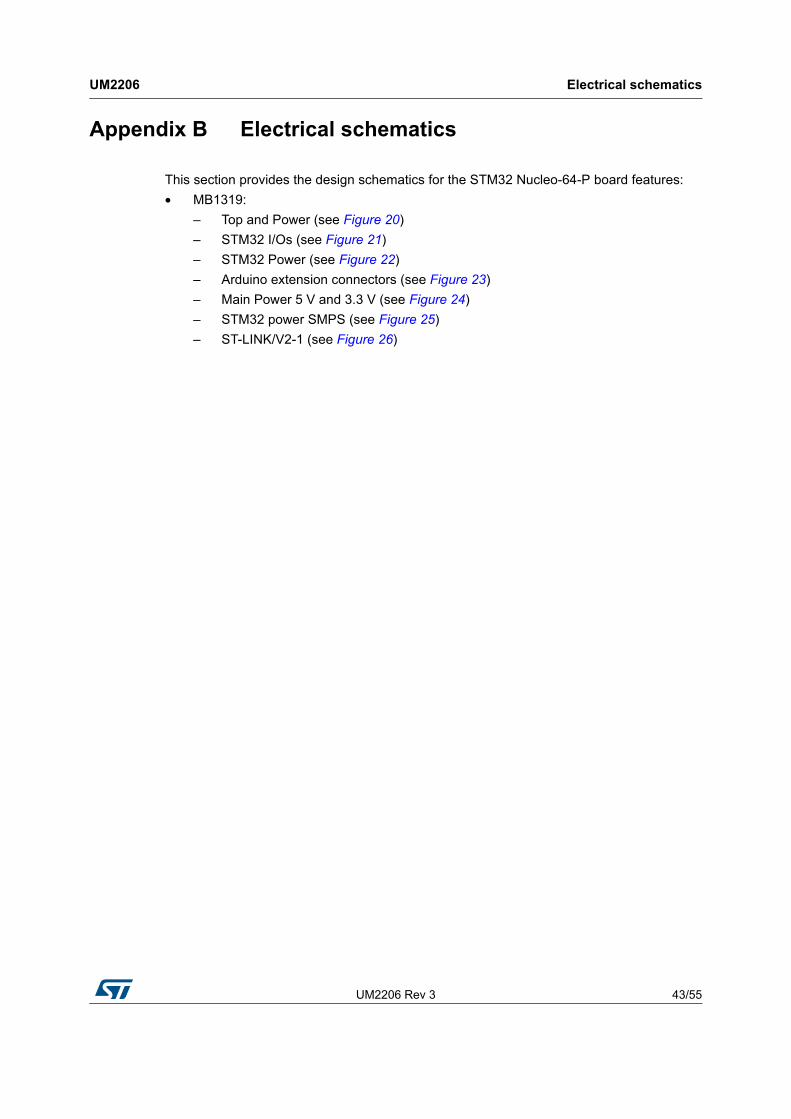
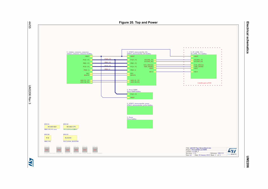
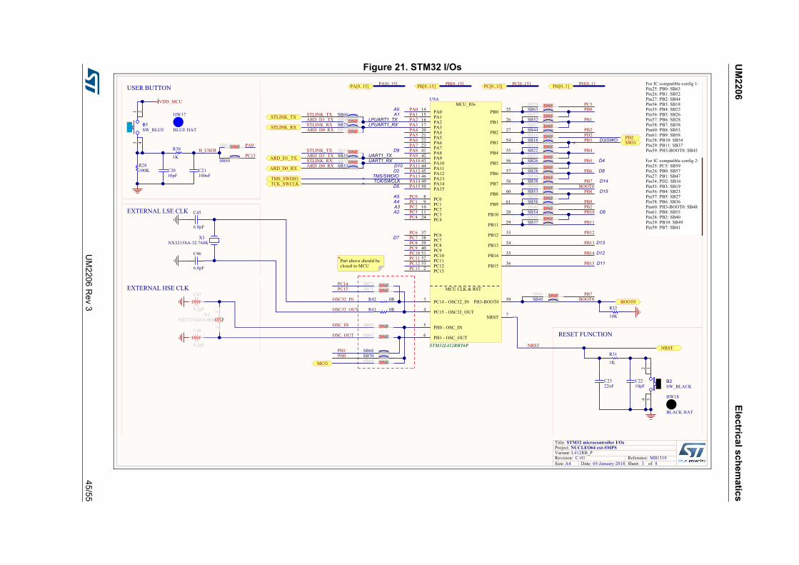
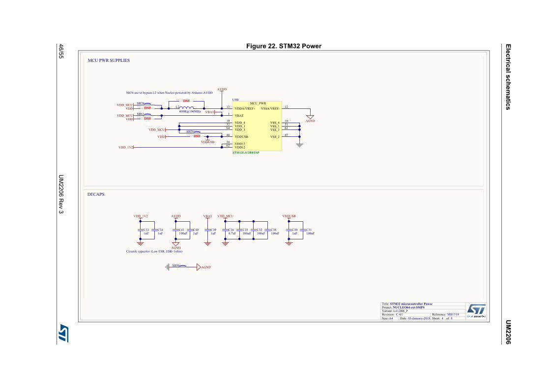
Appendix B Electrical schematics . . . . . . . . . . . . . . . . . . . . . . . . . . . . . . . . . . . . 43
Appendix C Federal Communications Commission (FCC) and Industry Canada (IC) Compliance . . . . . . . . . . . . . . . . . . . . . . . 51
C.1 FCC Compliance Statement . . . . . . . . . . . . . . . . . . . . . . . . . . . . . . . . . . . 51
C.1.1 Part 15.19 . . . . . . . . . . . . . . . . . . . . . . . . . . . . . . . . . . . . . . . . . . . . . . . . 51
C.1.2 Part 15.105 . . . . . . . . . . . . . . . . . . . . . . . . . . . . . . . . . . . . . . . . . . . . . . . 51
C.1.3 Part 15.21 . . . . . . . . . . . . . . . . . . . . . . . . . . . . . . . . . . . . . . . . . . . . . . . . 51
C.2 IC Compliance Statement . . . . . . . . . . . . . . . . . . . . . . . . . . . . . . . . . . . . . 51
C.2.1 Compliance Statement . . . . . . . . . . . . . . . . . . . . . . . . . . . . . . . . . . . . . . 52
C.2.2 Déclaration de conformité. . . . . . . . . . . . . . . . . . . . . . . . . . . . . . . . . . . . 52
Appendix D CISPR32 . . . . . . . . . . . . . . . . . . . . . . . . . . . . . . . . . . . . . . . . . . . . . . . 53
D.1 Warning . . . . . . . . . . . . . . . . . . . . . . . . . . . . . . . . . . . . . . . . . . . . . . . . . . . 53
Revision history . . . . . . . . . . . . . . . . . . . . . . . . . . . . . . . . . . . . . . . . . . . . . . . . . . . . 54
List of tables UM2206
4/55 UM2206 Rev 3
List of tables
Table 1. Ordering information . . . . . . . . . . . . . . . . . . . . . . . . . . . . . . . . . . . . . . . . . . . . . . . . . . . . . . . 7Table 2. Codification explanation . . . . . . . . . . . . . . . . . . . . . . . . . . . . . . . . . . . . . . . . . . . . . . . . . . . . 7Table 3. ON/OFF convention . . . . . . . . . . . . . . . . . . . . . . . . . . . . . . . . . . . . . . . . . . . . . . . . . . . . . . . 7Table 4. Default jumper settings . . . . . . . . . . . . . . . . . . . . . . . . . . . . . . . . . . . . . . . . . . . . . . . . . . . . 14Table 5. ST-LINK jumper configuration . . . . . . . . . . . . . . . . . . . . . . . . . . . . . . . . . . . . . . . . . . . . . . 15Table 6. Debug connector SWD . . . . . . . . . . . . . . . . . . . . . . . . . . . . . . . . . . . . . . . . . . . . . . . . . . . . 17Table 7. Power supply capabilities . . . . . . . . . . . . . . . . . . . . . . . . . . . . . . . . . . . . . . . . . . . . . . . . . . 18Table 8. SB9 configurations . . . . . . . . . . . . . . . . . . . . . . . . . . . . . . . . . . . . . . . . . . . . . . . . . . . . . . . 22Table 9. LPUART1 connection . . . . . . . . . . . . . . . . . . . . . . . . . . . . . . . . . . . . . . . . . . . . . . . . . . . . . 26Table 10. USART1 connection . . . . . . . . . . . . . . . . . . . . . . . . . . . . . . . . . . . . . . . . . . . . . . . . . . . . . . 26Table 11. Jumper settings . . . . . . . . . . . . . . . . . . . . . . . . . . . . . . . . . . . . . . . . . . . . . . . . . . . . . . . . . 28Table 12. Solder bridge configurations and settings. . . . . . . . . . . . . . . . . . . . . . . . . . . . . . . . . . . . . . 29Table 13. USB Micro-B pinout . . . . . . . . . . . . . . . . . . . . . . . . . . . . . . . . . . . . . . . . . . . . . . . . . . . . . . 33Table 14. Arduino connector pinout . . . . . . . . . . . . . . . . . . . . . . . . . . . . . . . . . . . . . . . . . . . . . . . . . . 35Table 15. External power connector pinout . . . . . . . . . . . . . . . . . . . . . . . . . . . . . . . . . . . . . . . . . . . . 39Table 16. NUCLEO-L412RB-P, NUCLEO-L433RC-P and NUCLEO-L452RE-P
I/O assignment . . . . . . . . . . . . . . . . . . . . . . . . . . . . . . . . . . . . . . . . . . . . . . . . . . . . . . . . . . 40Table 17. Document revision history . . . . . . . . . . . . . . . . . . . . . . . . . . . . . . . . . . . . . . . . . . . . . . . . . 54
UM2206 Rev 3 5/55
UM2206 List of figures
5
List of figures
Figure 1. Nucleo-64-P board (top view) . . . . . . . . . . . . . . . . . . . . . . . . . . . . . . . . . . . . . . . . . . . . . . . . 1Figure 2. Nucleo-64-P board (bottom view) . . . . . . . . . . . . . . . . . . . . . . . . . . . . . . . . . . . . . . . . . . . . . 1Figure 3. Hardware block diagram. . . . . . . . . . . . . . . . . . . . . . . . . . . . . . . . . . . . . . . . . . . . . . . . . . . 10Figure 4. STM32 Nucleo-64-P board top layout . . . . . . . . . . . . . . . . . . . . . . . . . . . . . . . . . . . . . . . . 11Figure 5. STM32 Nucleo-64-P board bottom layout . . . . . . . . . . . . . . . . . . . . . . . . . . . . . . . . . . . . . 12Figure 6. STM32 Nucleo-64 -P board mechanical drawing . . . . . . . . . . . . . . . . . . . . . . . . . . . . . . . . 13Figure 7. USB composite device . . . . . . . . . . . . . . . . . . . . . . . . . . . . . . . . . . . . . . . . . . . . . . . . . . . . 15Figure 8. ST-LINK debugger: jumper configuration for on-board MCU . . . . . . . . . . . . . . . . . . . . . . . 16Figure 9. ST-LINK debugger: jumper configuration for external MCU . . . . . . . . . . . . . . . . . . . . . . . . 17Figure 10. JP5[1-2]: 5V_STL power source. . . . . . . . . . . . . . . . . . . . . . . . . . . . . . . . . . . . . . . . . . . . . 19Figure 11. JP5[3-4]: 5V_VIN power source . . . . . . . . . . . . . . . . . . . . . . . . . . . . . . . . . . . . . . . . . . . . . 20Figure 12. JP5[5-6]: E5V power source . . . . . . . . . . . . . . . . . . . . . . . . . . . . . . . . . . . . . . . . . . . . . . . . 21Figure 13. JP6[7-8]: 5V_USB_CHG power source . . . . . . . . . . . . . . . . . . . . . . . . . . . . . . . . . . . . . . . 22Figure 14. USB Micro-B connector CN1 (front view) . . . . . . . . . . . . . . . . . . . . . . . . . . . . . . . . . . . . . . 33Figure 15. Arduino connectors. . . . . . . . . . . . . . . . . . . . . . . . . . . . . . . . . . . . . . . . . . . . . . . . . . . . . . . 34Figure 16. Arduino connector pinout . . . . . . . . . . . . . . . . . . . . . . . . . . . . . . . . . . . . . . . . . . . . . . . . . . 35Figure 17. ST morpho connector . . . . . . . . . . . . . . . . . . . . . . . . . . . . . . . . . . . . . . . . . . . . . . . . . . . . . 37Figure 18. ST morpho connector pinout . . . . . . . . . . . . . . . . . . . . . . . . . . . . . . . . . . . . . . . . . . . . . . . 38Figure 19. External power connector . . . . . . . . . . . . . . . . . . . . . . . . . . . . . . . . . . . . . . . . . . . . . . . . . . 39Figure 20. Top and Power . . . . . . . . . . . . . . . . . . . . . . . . . . . . . . . . . . . . . . . . . . . . . . . . . . . . . . . . . . 44Figure 21. STM32 I/Os. . . . . . . . . . . . . . . . . . . . . . . . . . . . . . . . . . . . . . . . . . . . . . . . . . . . . . . . . . . . . 45Figure 22. STM32 Power . . . . . . . . . . . . . . . . . . . . . . . . . . . . . . . . . . . . . . . . . . . . . . . . . . . . . . . . . . . 46Figure 23. Arduino extension connectors . . . . . . . . . . . . . . . . . . . . . . . . . . . . . . . . . . . . . . . . . . . . . . 47Figure 24. Main Power 5 V, 3.3 V . . . . . . . . . . . . . . . . . . . . . . . . . . . . . . . . . . . . . . . . . . . . . . . . . . . . 48Figure 25. STM32 power SMPS . . . . . . . . . . . . . . . . . . . . . . . . . . . . . . . . . . . . . . . . . . . . . . . . . . . . . 49Figure 26. ST-LINK/V2-1 . . . . . . . . . . . . . . . . . . . . . . . . . . . . . . . . . . . . . . . . . . . . . . . . . . . . . . . . . . . 50
Features UM2206
6/55 UM2206 Rev 3
1 Features
• STM32 Arm®(a)-based microcontroller in LQFP64 package
• SMPS: significantly reduces power consumption in Run mode
• 32.768 kHz LSE crystal oscillator
• One user LED shared with Arduino™
• Two push-buttons: USER and RESET
• Board expansion connectors:
– Arduino™ Uno V3
– ST morpho
– External SMPS experimentation dedicated connector
• Flexible board power supply: ST-LINK/V2-1 USB VBUS or external sources
• On-board ST-LINK/V2-1 debugger/programmer with USB re-enumeration capability: mass storage, Virtual COM port and debug port
• Comprehensive free software libraries and examples available with the STM32Cube package
• Support of a wide choice of Integrated Development Environments (IDEs) including IAR™, Keil®, GCC-based IDEs
2 Product marking
Evaluation tools marked as "ES" or "E" are not yet qualified and therefore they are not ready to be used as reference design or in production. Any consequences deriving from such usage will not be at ST charge. In no event, ST will be liable for any customer usage of these engineering sample tools as reference design or in production.
"E" or "ES" marking examples of location:
• On the targeted STM32 that is soldered on the board (for illustration of STM32 marking, refer to the section “Package characteristics” of the STM32 datasheet at www.st.com).
• Next to the evaluation tool ordering part number, that is stuck or silk-screen printed on the board.
This board features a specific STM32 device version, which allows the operation of any bundled commercial stack/library available. This STM32 device shows a "U" marking option at the end of the standard part number and is not available for sales. In order to use the same commercial stack in his application, a developer may need to purchase a part number specific to this stack/library. The price of those part numbers includes the stack/library royalties.
a. Arm is a registered trademark of Arm Limited (or its subsidiaries) in the US and or elsewhere.
UM2206 Rev 3 7/55
UM2206 Ordering information
54
3 Ordering information
To order the Nucleo-64-P board corresponding to the targeted STM32, refer to Table 1.
The meaning of the codification is explained in Table 2.
This order code is mentioned on a sticker placed on bottom side of the board.
4 Conventions
Table 3 provides the conventions used for the ON and OFF settings in the present document.
In this document the references for all information that is common to all sale types, are “STM32 Nucleo-64-P board” and “STM32 Nucleo-64-P boards”.
Table 1. Ordering information
Order code Target STM32
NUCLEO-L412RB-P STM32L412RBT6P
NUCLEO-L433RC-P STM32L433RCT6P
NUCLEO-L452RE-P STM32L452RET6P
Table 2. Codification explanation
NUCLEO-LxxxRy-P Description Example: NUCLEO-L452RE-P
Lxxx STM32 Product line STM32L452
R STM32 package pin count 64 pins
y
STM32 Flash memory size (8 for 64 Kbytes, B for 128 Kbytes, C for 256 Kbytes, E for 512 Kbytes, G for 1MKbyte, H for 1.5 Mbytes and I for 2 Mbytes)
E = 512 Kbytes
-P External SMPS architecture.
Table 3. ON/OFF convention
Convention Definition
Jumper JPx ON Jumper fitted
Jumper JPx OFF Jumper not fitted
Jumper JPx [1-2] Jumper should be fitted between Pin 1 and Pin 2
Solder bridge SBx ON SBx connections closed by 0 ohm resistor
Solder bridge SBx OFF SBx connections left open
System requirements UM2206
8/55 UM2206 Rev 3
5 System requirements
• Windows® OS (7, 8 and 10), Linux® or macOS®(a)
• USB Type-A to Micro-B cable
6 Development toolchains
• Keil® MDK-ARM(b)
• IAR™ EWARM(b)
• GCC-based IDEs including free SW4STM32 from AC6
7 Demonstration software
The demonstration software, included in the STM32Cube MCU Package, is preloaded in the STM32 Flash memory for easy demonstration of the device peripherals in standalone mode. The latest versions of the demonstration source code and associated documentation can be downloaded from the www.st.com/stm32nucleo webpage.
a. macOS® is a trademark of Apple Inc.\nregistered in the U.S. and other countries.
b. On Windows® only.
UM2206 Rev 3 9/55
UM2206 Quick start
54
8 Quick start
This section describes how to start a development quickly using the STM32 Nucleo-64-P board.
Before installing and using the product, accept the Evaluation Product License Agreement from the www.st.com/epla webpage.
8.1 Getting started
The STM32 Nucleo-64-P board is a low-cost and easy-to-use development kit to quickly evaluate and start a development with an STM32 microcontroller in QFP64 package. To start using this board, follow the steps below:
1. Check the jumper position on the board, as showed in the Table 4: Default jumper settings
2. For a correct identification of all device interfaces from the host PC, install the Nucleo USB driver available on the www.st.com/ stm32nucleo webpage, prior connecting the board.
3. To power the board connect the Nucleo-64-P board to a PC with a USB cable ‘type A to micro-B’ through the USB connector CN1. As a result the green LED LD3 (5 V PWR) lights up, LD1 (COM) and green LED LD4 blink.
4. Press user button B1 (blue).
5. Observe that the blinking frequency of the three green LED LD4 changes, by clicking on the button B1.
6. The software demonstration and the several software examples, that allow the user to use the Nucleo features, are available at the www.st.com/stm32nucleo webpage.
7. Develop an application using the available examples.
Hardware layout and configuration UM2206
10/55 UM2206 Rev 3
9 Hardware layout and configuration
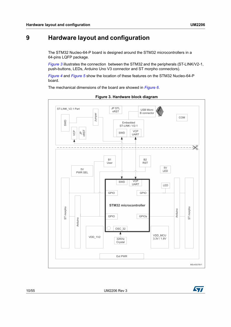
The STM32 Nucleo-64-P board is designed around the STM32 microcontrollers in a 64-pins LQFP package.
Figure 3 illustrates the connection between the STM32 and the peripherals (ST-LINK/V2-1, push-buttons, LEDs, Arduino Uno V3 connector and ST morpho connectors).
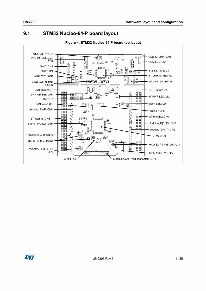
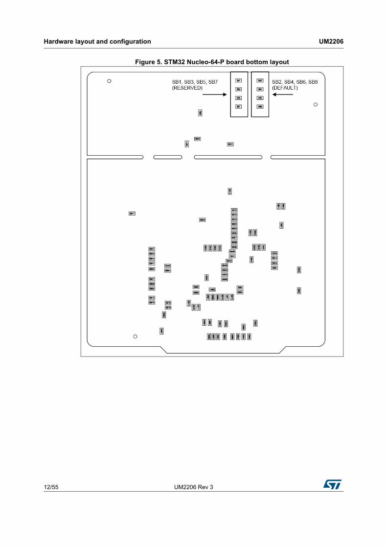
Figure 4 and Figure 5 show the location of these features on the STM32 Nucleo-64-P board.
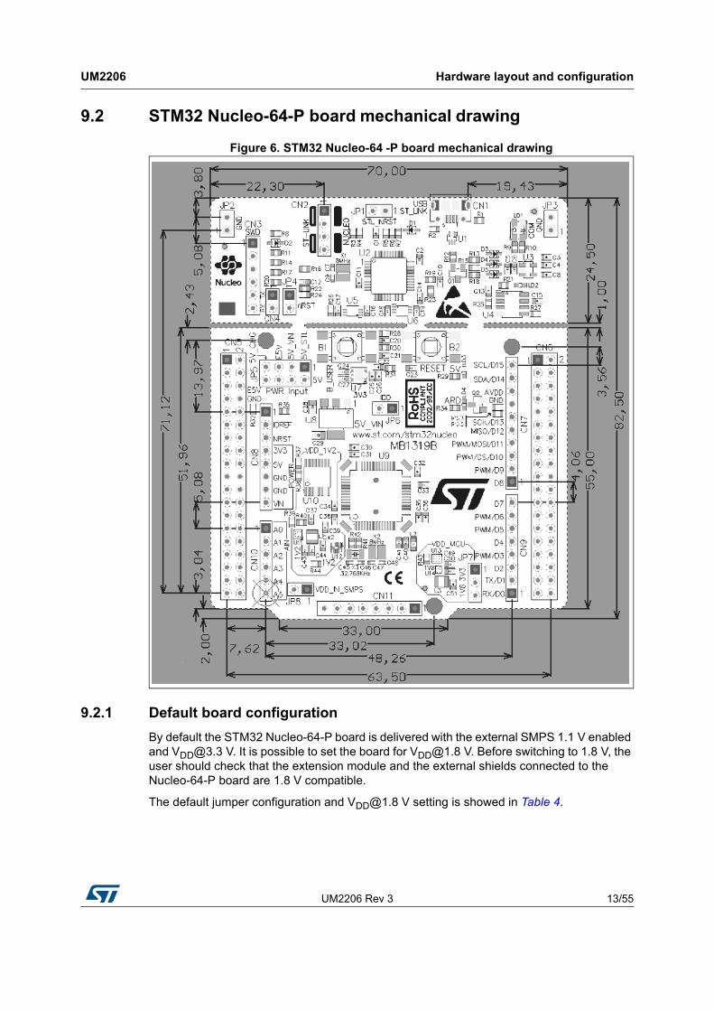
The mechanical dimensions of the board are showed in Figure 6.
Figure 3. Hardware block diagram
UM2206 Rev 3 11/55
UM2206 Hardware layout and configuration
54
9.1 STM32 Nucleo-64-P board layout
Figure 4. STM32 Nucleo-64-P board top layout
IDD JP: JP6
Arduino_D[8..15]: CN7
Arduino_D[0..7]: CN9
Arduino_A[0..5]: CN10
Arduino_PWR: CN8
SMPS_1V1: U11/U12
ST-LINK STM32: U2
User button: B1
UART VPN: CN4
SWD: CN3
USB_STLINK: CN1
5V PWR SEL: JP5
STLINK_5V_SW: U4
ST-LINK debugger: CN2
STLINK_3V3: U3
5V PWR LED: LD3
ST morpho: CN6
MCU 1V8 / 3V3: JP7
MCU SMPS 1V8: U13/U14
RST Button: B2
ST morpho: CN5
VIN to 5V: U8
3V3: U7
SMPS_1V2 SW: U10
VDD1V2_SMPS_IN: JP8
32KHz: X3
ST-LINK RST: JP1
User_LED: LD4
External Core PWR connector: CN11
SWD level shifter:U5/U6
nRST: JP4
COM LED: LD1
STM32: U9
Hardware layout and configuration UM2206
12/55 UM2206 Rev 3
Figure 5. STM32 Nucleo-64-P board bottom layout
UM2206 Rev 3 13/55
UM2206 Hardware layout and configuration
54
9.2 STM32 Nucleo-64-P board mechanical drawing
Figure 6. STM32 Nucleo-64 -P board mechanical drawing
9.2.1 Default board configuration
By default the STM32 Nucleo-64-P board is delivered with the external SMPS 1.1 V enabled and [email protected] V. It is possible to set the board for [email protected] V. Before switching to 1.8 V, the user should check that the extension module and the external shields connected to the Nucleo-64-P board are 1.8 V compatible.
The default jumper configuration and [email protected] V setting is showed in Table 4.
Hardware layout and configuration UM2206
14/55 UM2206 Rev 3
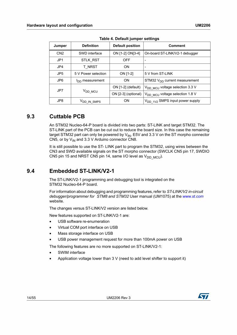
9.3 Cuttable PCB
An STM32 Nucleo-64-P board is divided into two parts: ST-LINK and target STM32. The ST-LINK part of the PCB can be cut out to reduce the board size. In this case the remaining target STM32 part can only be powered by VIN, E5V and 3.3 V on the ST morpho connector CN5, or by VIN and 3.3 V Arduino connector CN8.
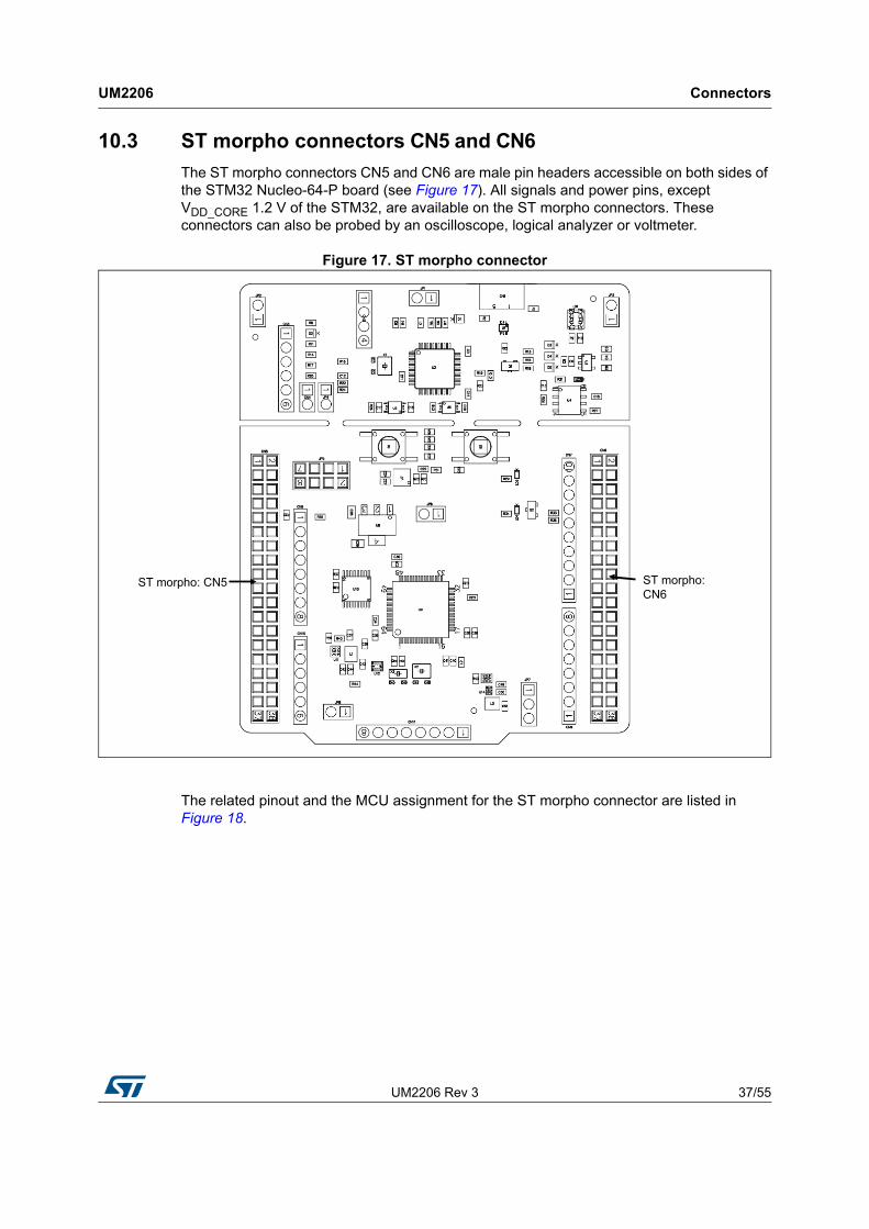
It is still possible to use the ST- LINK part to program the STM32, using wires between the CN3 and SWD available signals on the ST morpho connector (SWCLK CN5 pin 17, SWDIO CN5 pin 15 and NRST CN5 pin 14, same I/O level as VDD_MCU).
9.4 Embedded ST-LINK/V2-1
The ST-LINK/V2-1 programming and debugging tool is integrated on the STM32 Nucleo-64-P board.
For information about debugging and programming features, refer to ST-LINK/V2 in-circuit debugger/programmer for STM8 and STM32 User manual (UM1075) at the www.st.com website.
The changes versus ST-LINK/V2 version are listed below.
New features supported on ST-LINK/V2-1 are:
• USB software re-enumeration
• Virtual COM port interface on USB
• Mass storage interface on USB
• USB power management request for more than 100mA power on USB
The following features are no more supported on ST-LINK/V2-1:
• SWIM interface
• Application voltage lower than 3 V (need to add level shifter to support it)
Table 4. Default jumper settings
Jumper Definition Default position Comment
CN2 SWD interface ON [1-2] ON[3-4] On-board ST-LINK/V2-1 debugger
JP1 STLK_RST OFF -
JP4 T_NRST ON -
JP5 5 V Power selection ON [1-2] 5 V from ST-LINK
JP6 IDD measurement ON STM32 VDD current measurement
JP7 VDD_MCU
ON [1-2] (default) VDD_MCU voltage selection 3.3 V
ON [2-3] (optional) VDD_MCU voltage selection 1.8 V
JP8 VDD_IN_SMPS ON VDD_1V2 SMPS input power supply
UM2206 Rev 3 15/55
UM2206 Hardware layout and configuration
54
The embedded ST-LINK/V2-1 can be used in two different ways according to the jumper states (refer to Table 5):
• Program/debug the STM32 on board,
• Program/debug an STM32 in an external application board using a cable connected to SWD connector.
9.4.1 Drivers
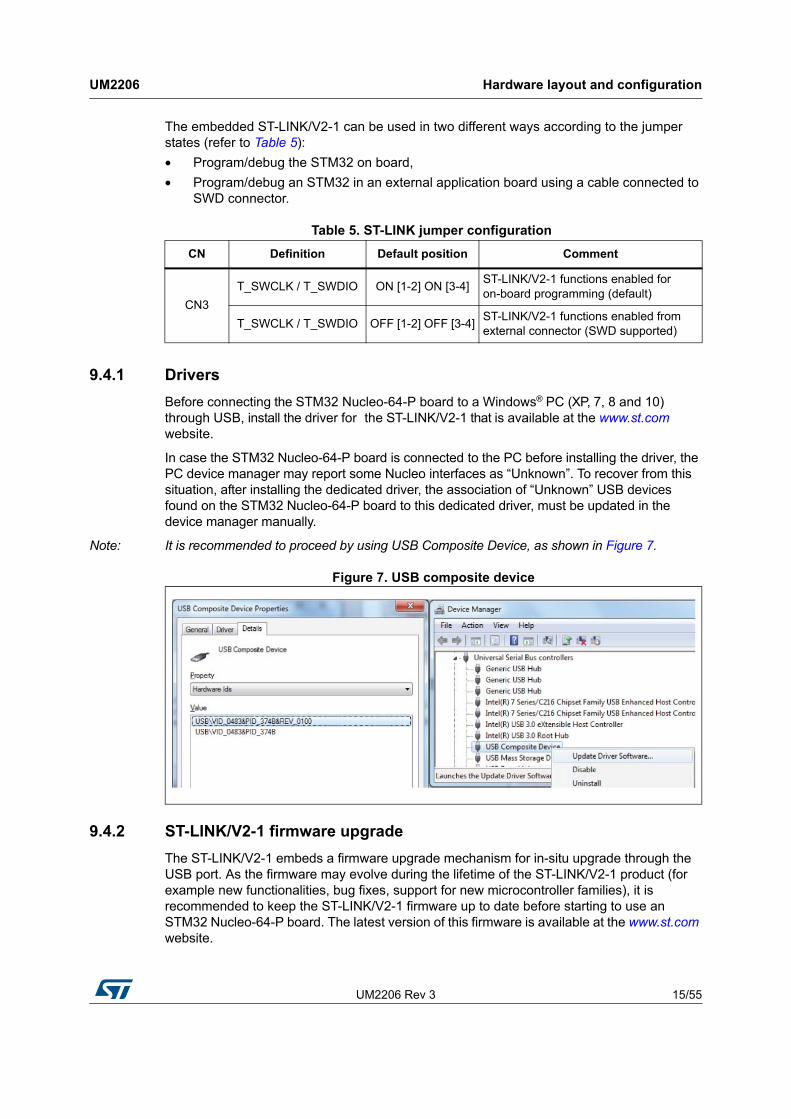
Before connecting the STM32 Nucleo-64-P board to a Windows® PC (XP, 7, 8 and 10) through USB, install the driver for the ST-LINK/V2-1 that is available at the www.st.com website.
In case the STM32 Nucleo-64-P board is connected to the PC before installing the driver, the PC device manager may report some Nucleo interfaces as “Unknown”. To recover from this situation, after installing the dedicated driver, the association of “Unknown” USB devices found on the STM32 Nucleo-64-P board to this dedicated driver, must be updated in the device manager manually.
Note: It is recommended to proceed by using USB Composite Device, as shown in Figure 7.
Figure 7. USB composite device
9.4.2 ST-LINK/V2-1 firmware upgrade
The ST-LINK/V2-1 embeds a firmware upgrade mechanism for in-situ upgrade through the USB port. As the firmware may evolve during the lifetime of the ST-LINK/V2-1 product (for example new functionalities, bug fixes, support for new microcontroller families), it is recommended to keep the ST-LINK/V2-1 firmware up to date before starting to use an STM32 Nucleo-64-P board. The latest version of this firmware is available at the www.st.com website.
Table 5. ST-LINK jumper configuration
CN Definition Default position Comment
CN3
T_SWCLK / T_SWDIO ON [1-2] ON [3-4]ST-LINK/V2-1 functions enabled for on-board programming (default)
T_SWCLK / T_SWDIO OFF [1-2] OFF [3-4]ST-LINK/V2-1 functions enabled from external connector (SWD supported)
Hardware layout and configuration UM2206
16/55 UM2206 Rev 3
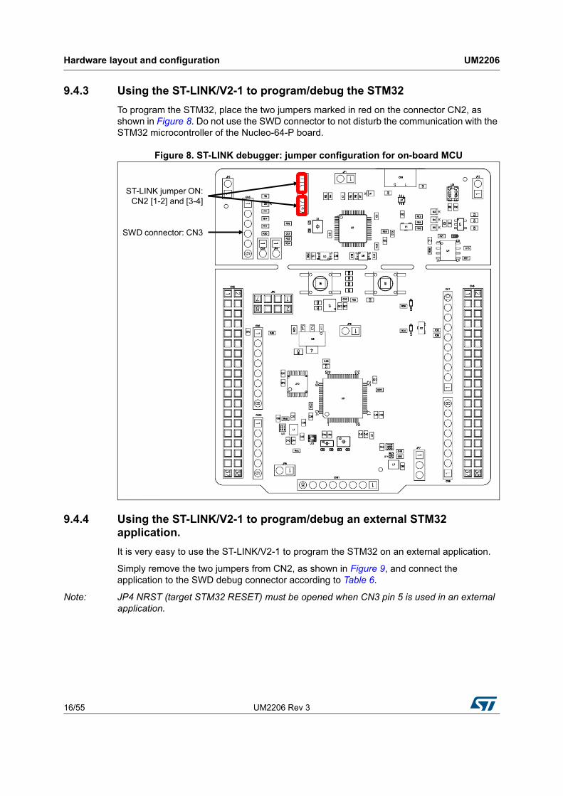
9.4.3 Using the ST-LINK/V2-1 to program/debug the STM32
To program the STM32, place the two jumpers marked in red on the connector CN2, as shown in Figure 8. Do not use the SWD connector to not disturb the communication with the STM32 microcontroller of the Nucleo-64-P board.
Figure 8. ST-LINK debugger: jumper configuration for on-board MCU
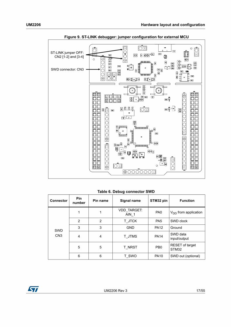
9.4.4 Using the ST-LINK/V2-1 to program/debug an external STM32 application.
It is very easy to use the ST-LINK/V2-1 to program the STM32 on an external application.
Simply remove the two jumpers from CN2, as shown in Figure 9, and connect the application to the SWD debug connector according to Table 6.
Note: JP4 NRST (target STM32 RESET) must be opened when CN3 pin 5 is used in an external application.
SWD connector: CN3
ST-LINK jumper ON: CN2 [1-2] and [3-4]
UM2206 Rev 3 17/55
UM2206 Hardware layout and configuration
54
Figure 9. ST-LINK debugger: jumper configuration for external MCU
Table 6. Debug connector SWD
ConnectorPin
numberPin name Signal name STM32 pin Function
SWD
CN3
1 1VDD_TARGET:
AIN_1PA0 VDD from application
2 2 T_JTCK PA5 SWD clock
3 3 GND PA12 Ground
4 4 T_JTMS PA14SWD data input/output
5 5 T_NRST PB0RESET of target STM32
6 6 T_SWO PA10 SWD out (optional)
SWD connector: CN3
ST-LINK jumper OFF:CN2 [1-2] and [3-4]
Hardware layout and configuration UM2206
18/55 UM2206 Rev 3
9.5 Power supply and power selection
9.5.1 External Power supply input
The STM32 Nucleo-64-P board is designed to be powered by several DC power supply. It is possible to supply the STM32 Nucleo-64-P board with any of the following sources:
• 5V_ST_LINK from ST-LINK USB connector
• VIN (7 V-12 V) from Arduino connector or ST morpho connector
• E5V from ST morpho connector
• 5V_USB_CHARGER from ST-LINK USB
• 3.3 V on Arduino connector or ST morpho connector
Note: If an external 5V DC power source is used, the Discovery board must be powered by a power supply unit or by an auxiliary equipment complying with the standard EN-60950-1: 2006+A11/2009 and must be Safety Extra Low Voltage (SELV) with limited power capability.
The power supply capabilities are showed in Table 7.
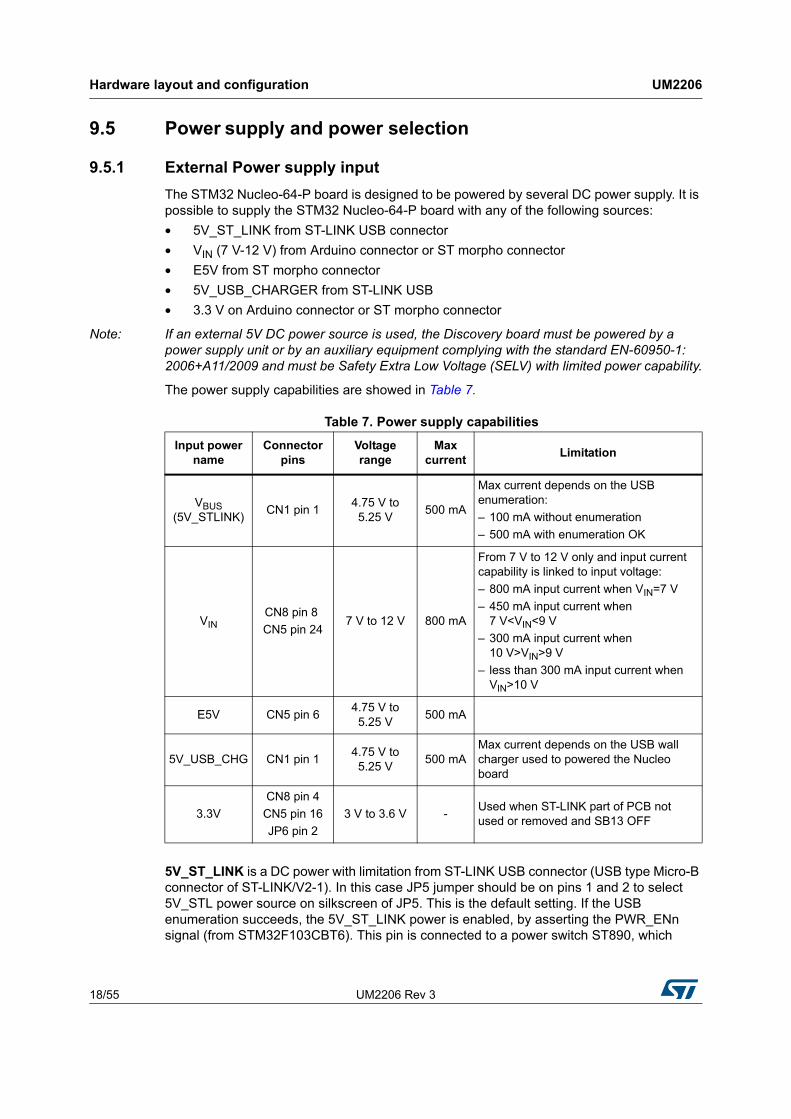
5V_ST_LINK is a DC power with limitation from ST-LINK USB connector (USB type Micro-B connector of ST-LINK/V2-1). In this case JP5 jumper should be on pins 1 and 2 to select 5V_STL power source on silkscreen of JP5. This is the default setting. If the USB enumeration succeeds, the 5V_ST_LINK power is enabled, by asserting the PWR_ENn signal (from STM32F103CBT6). This pin is connected to a power switch ST890, which
Table 7. Power supply capabilities
Input power name
Connector pins
Voltagerange
Max current
Limitation
VBUS (5V_STLINK)
CN1 pin 1 4.75 V to 5.25 V
500 mA
Max current depends on the USB enumeration:
– 100 mA without enumeration
– 500 mA with enumeration OK
VINCN8 pin 8
CN5 pin 247 V to 12 V 800 mA
From 7 V to 12 V only and input current capability is linked to input voltage:
– 800 mA input current when VIN=7 V
– 450 mA input current when 7 V<VIN<9 V
– 300 mA input current when 10 V>VIN>9 V
– less than 300 mA input current when VIN>10 V
E5V CN5 pin 64.75 V to 5.25 V
500 mA
5V_USB_CHG CN1 pin 1 4.75 V to 5.25 V
500 mAMax current depends on the USB wall charger used to powered the Nucleo board
3.3V
CN8 pin 4
CN5 pin 16
JP6 pin 2
3 V to 3.6 V -Used when ST-LINK part of PCB not used or removed and SB13 OFF
UM2206 Rev 3 19/55
UM2206 Hardware layout and configuration
54
powers the board. This power switch also features a current limitation to protect the PC in case of a short-circuit on board (more than 750 mA).
The STM32 Nucleo-64-P board and its shield can be powered from the ST-LINK USB connector CN1, but only ST-LINK circuit is powered before USB enumeration, because the host PC only provides 100 mA to the board at that time. During the USB enumeration, STM32 Nucleo-64-P board requires 500 mA of current to the host PC. If the host is able to provide the required power, the enumeration ends by a “SetConfiguration” command and then, the power transistor ST890 is switched ON, the green LED LD3 is turned ON, thus the STM32 Nucleo-64-P board and its shield request no more than 500 mA current. If the host is not able to provide the required current, the enumeration fails. Therefore the power switch ST890 stays OFF and the MCU part including the extension board is not powered. As a consequence the green LED LD3 stays turned OFF. In this case it is mandatory to use an external power supply.
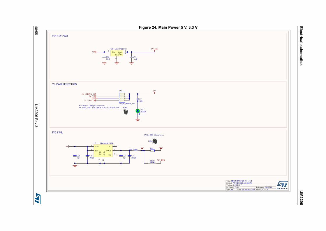
USB power: 5V_STL configuration: jumper JP5[1-2] should be connected as showed in Figure 10.
Figure 10. JP5[1-2]: 5V_STL power source
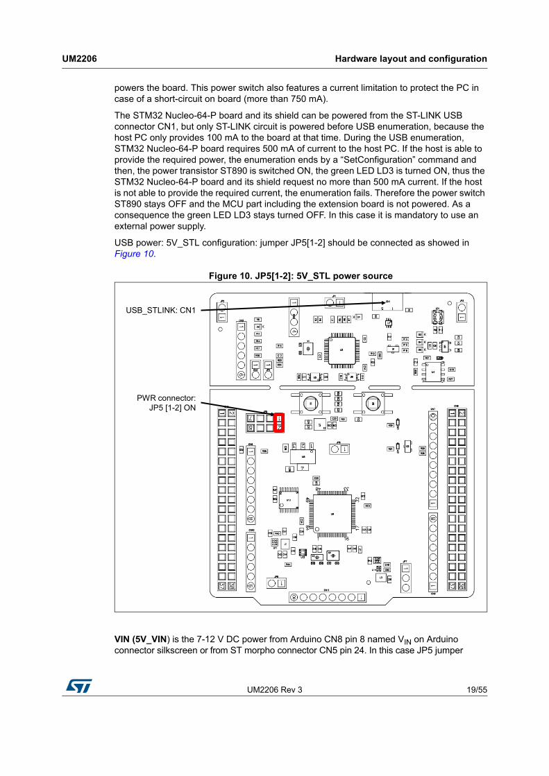
VIN (5V_VIN) is the 7-12 V DC power from Arduino CN8 pin 8 named VIN on Arduino connector silkscreen or from ST morpho connector CN5 pin 24. In this case JP5 jumper
PWR connector:JP5 [1-2] ON
USB_STLINK: CN1
Hardware layout and configuration UM2206
20/55 UM2206 Rev 3
should be on pins 3 and 4 to select 5V_VIN power source on silkscreen of JP5. In that case the DC power comes from the power supply through the Arduino Uno V3 battery shield (compatible with Adafruit PowerBoost 500 shield).
5V_VIN configuration: jumper JP5[3-4] should be connected as showed in Figure 11.
Figure 11. JP5[3-4]: 5V_VIN power source
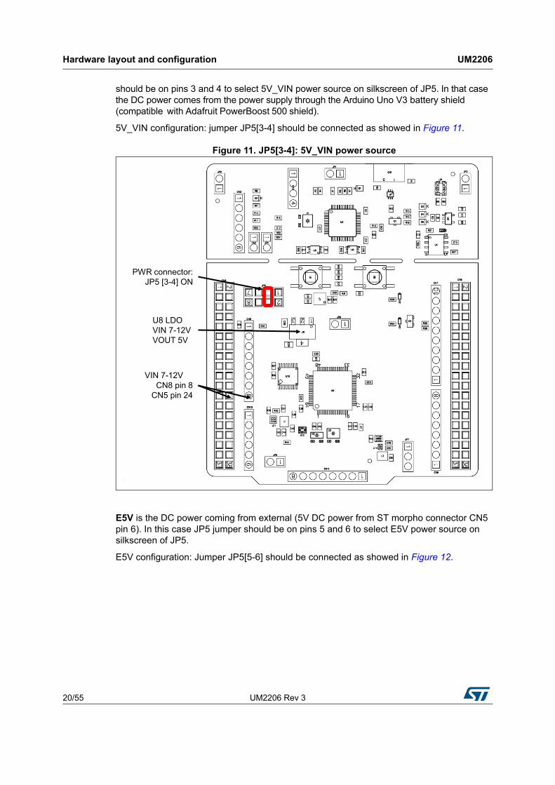
E5V is the DC power coming from external (5V DC power from ST morpho connector CN5 pin 6). In this case JP5 jumper should be on pins 5 and 6 to select E5V power source on silkscreen of JP5.
E5V configuration: Jumper JP5[5-6] should be connected as showed in Figure 12.
VIN 7-12VCN8 pin 8
CN5 pin 24
U8 LDOVIN 7-12VVOUT 5V
PWR connector:JP5 [3-4] ON
UM2206 Rev 3 21/55
UM2206 Hardware layout and configuration
54
Figure 12. JP5[5-6]: E5V power source
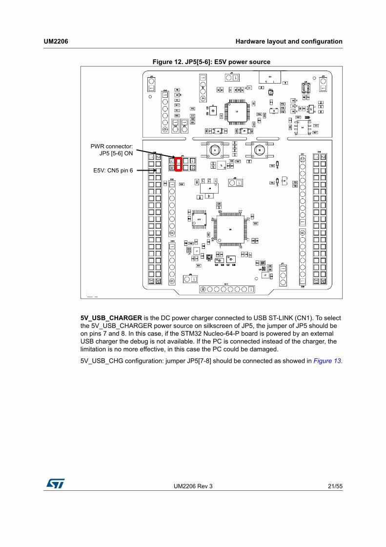
5V_USB_CHARGER is the DC power charger connected to USB ST-LINK (CN1). To select the 5V_USB_CHARGER power source on silkscreen of JP5, the jumper of JP5 should be on pins 7 and 8. In this case, if the STM32 Nucleo-64-P board is powered by an external USB charger the debug is not available. If the PC is connected instead of the charger, the limitation is no more effective, in this case the PC could be damaged.
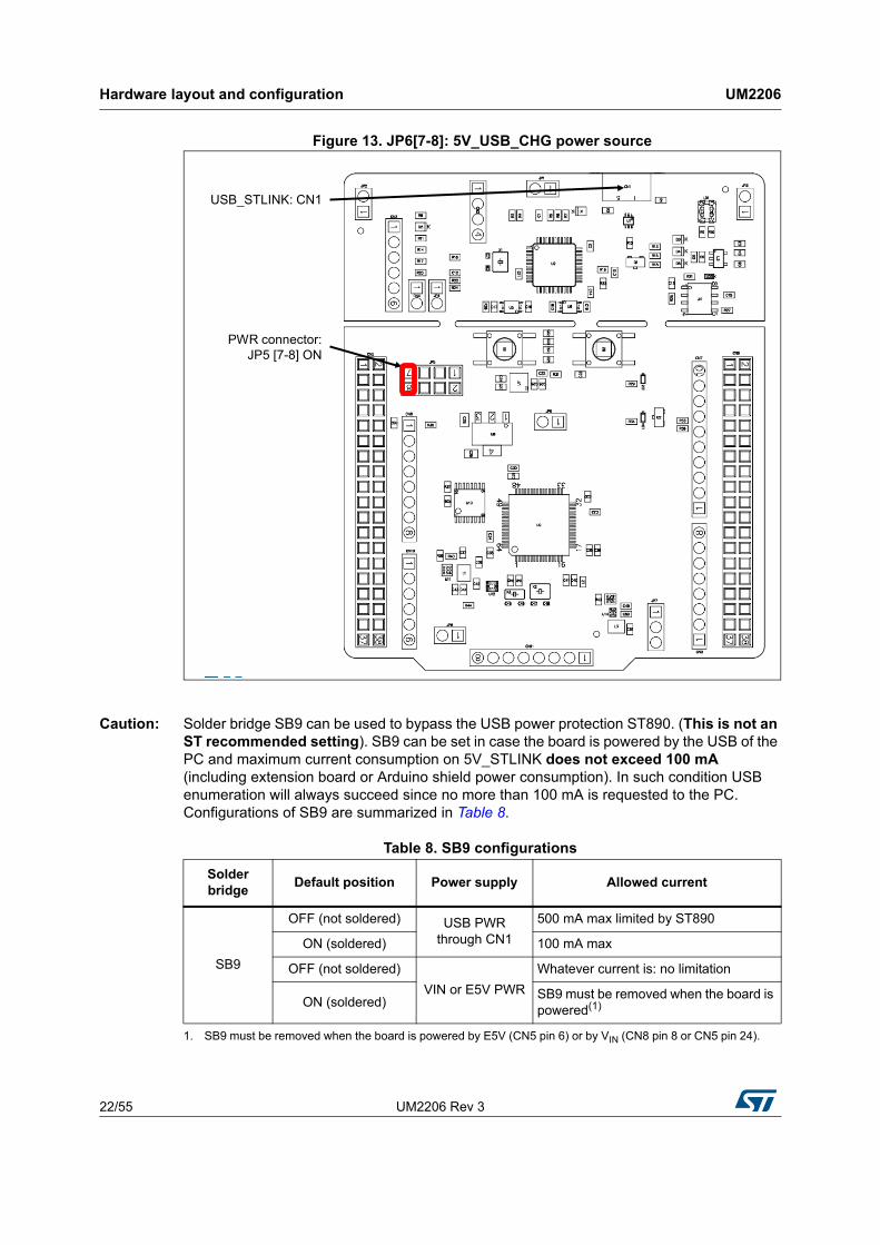
5V_USB_CHG configuration: jumper JP5[7-8] should be connected as showed in Figure 13.
E5V: CN5 pin 6
PWR connector:JP5 [5-6] ON
Hardware layout and configuration UM2206
22/55 UM2206 Rev 3
Figure 13. JP6[7-8]: 5V_USB_CHG power source
Caution: Solder bridge SB9 can be used to bypass the USB power protection ST890. (This is not an ST recommended setting). SB9 can be set in case the board is powered by the USB of the PC and maximum current consumption on 5V_STLINK does not exceed 100 mA (including extension board or Arduino shield power consumption). In such condition USB enumeration will always succeed since no more than 100 mA is requested to the PC. Configurations of SB9 are summarized in Table 8.
PWR connector:JP5 [7-8] ON
USB_STLINK: CN1
Table 8. SB9 configurations
Solder bridge
Default position Power supply Allowed current
SB9
OFF (not soldered) USB PWR through CN1
500 mA max limited by ST890
ON (soldered) 100 mA max
OFF (not soldered)
VIN or E5V PWR
Whatever current is: no limitation
ON (soldered)SB9 must be removed when the board is powered(1)
1. SB9 must be removed when the board is powered by E5V (CN5 pin 6) or by VIN (CN8 pin 8 or CN5 pin 24).

UM2206 Rev 3 23/55
UM2206 Hardware layout and configuration
54
Warning: In case the maximum current consumption of the STM32 Nucleo-64-P board and its extension boards exceeds 500 mA, it is recommended to power the STM32 Nucleo-64-P board using an external power supply connected to E5V or VIN.
9.5.2 External power supply output
5 V: the 5 V (CN8 pin 5 or CN5 pin 18) can be used as output power supply for an Arduino shield or an extension board, when the STM32 Nucleo-64-P board is powered by USB, VIN or E5V. In this case the maximum current allowed is showed in Table 7.
3.3 V: on CN8 pin 4 or CN5 pin 16 can be also used as power supply output. The current is limited by the maximum current capability of the regulator U7 (LD39050PUR33 from STMicroelectronics). In this condition the maximum consumption of the STM32 Nucleo-64-P board and the connected shield should be less than 500 mA.
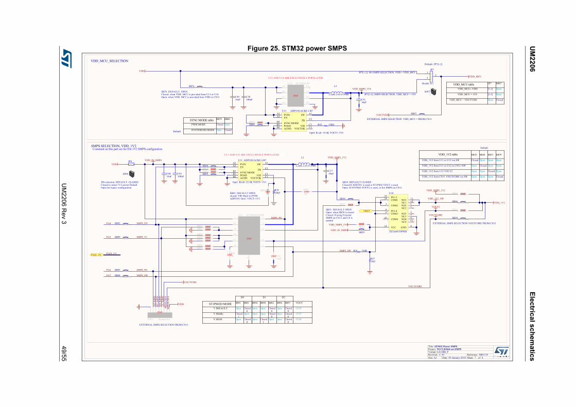
9.5.3 SMPS power supply
Power figures in Run mode are significantly improved by:
• Generating Vcore logic supply from an external SMPS (switched-mode power supply) or from an external connector
• Generating VDD_MCU supply from an external SMPS (switched-mode power supply), or from an external connector
The STM32 Nucleo-64-P board is populated with two SMPSs, U11 and U13, with the following functions:
• SMPS U11 allows to supply dynamically the VDD_1V2 pins in Run mode at 1.1 V with a maximum current of 30 mA.
• SMPS U13 allows to supply the VDD_MCU pin at 1.8 V with a maximum current of 50 mA (hysteresis operation mode). The SMPS U13 can deliver higher current (PWM operation mode) but with less efficiency. To set the U13 SMPS in PWM mode remove SB80 and solder SB79. This SMPS is enabled by default.
VDD_MCU configuration:
• 3.3 V (default): JP7 to pins 1 and 2
• 1.8 V: JP7 to pins 2 and 3 (best ULPBench score)
Note: The ST-LINK is still available in this configuration thanks to the level shifters U5 and U6.
For all general information concerning design recommendations for the STM32 with external SMPS, refer to the Design recommendations for STM32L4xxxx with external SMPS, design guide for ultra-low-power applications with performance Application note (AN4978) available at the www.st.com website.
Hardware layout and configuration UM2206
24/55 UM2206 Rev 3
9.6 Programming/debugging when the power supply is not from ST-LINK (5V_ST_link)
VIN or E5V is used as an external power supply in case the current consumption of the STM32 Nucleo-64-P board and its extension boards exceed the allowed current on the USB. In such condition it is still possible to use the USB for communication, programming or debugging only.
In this case it is mandatory to power the board first using VIN or E5V then to connect the USB cable to the PC. Proceeding this way the enumeration succeeds, thanks to the external power source.
The following power sequence procedure must be respected:
1. Connect jumper JP5 between pins 3 and 4 for VIN or pins 5 and 6 for E5V
2. Be sure that SB9 is removed
3. Connect the external power source to VIN or E5V
4. Power ON the external power supply 7 V< VIN < 12 V to VIN, or 5 V for E5V
5. Check that the green LED LD3 is turned ON
6. Connect the PC to the USB connector CN1
If this sequence is not respected, the board may be powered by VBUS first from the ST-LINK, with the following risks:
• If more than 500 mA current is needed by the board, the PC may be damaged or the current supplied may be limited by the PC. As a consequence the board is not powered correctly.
• 500 mA is requested at the enumeration (since SB9 must be OFF): this request can be rejected and the enumeration does not succeed if the PC cannot provide such current, consequently the board is not power supplied (LED LD3 remains OFF).
9.7 OSC clock sources
Three clock sources are listed below:
• LSE which is the 32.768 KHz crystal for the STM32 embedded RTC
• MCO which is the 8 MHz clock from the ST-LINK MCU for the STM32 microcontroller
• HSE which is the 8 MHz oscillator for the STM32 microcontroller. This clock is not implemented on the STM32 Nucleo-64-P board.
9.7.1 LSE: OSC 32 KHz clock supply
There are three ways to configure the pins corresponding to the low-speed clock (LSE):
LSE on-board oscillator X3 crystal (Default configuration). Refer to Oscillator design guide for STM8S, STM8A and STM32 microcontrollers Application note (AN2867) for oscillator design guide for STM32 microcontrollers. It is recommended to use NX3215SA manufactured by NDK (32.768 kHz, 6 pF, 20 ppm).
Oscillator from external to PC14 input: from external oscillator through pin 25 of the CN5 connector.
UM2206 Rev 3 25/55
UM2206 Hardware layout and configuration
54
The following configuration is needed:
• SB71 and SB72 ON
• R41 and R42 removed
LSE not used: PC14 and PC15 are used as GPIOs instead as low-speed clock.
The following configuration is needed:
• SB71 and SB72 ON
• R41 and R42 removed
9.7.2 OSC clock supply
There are four ways to configure the pins corresponding to the external-high-speed clock (HSE):
MCO from ST-LINK (Default: not connected): MCO output of ST-LINK MCU is used as an input clock. This frequency cannot be changed, it is fixed at 8 MHz and connected to PH0 OSC_IN of the STM32 microcontroller.
The following configuration is needed:
• SB67, SB69 and SB70 OFF
• SB64 ON
In this configuration PH1 is used as I/O (SB68 ON)
HSE: on-board oscillator X2 crystal (Default: not connected): for typical frequencies and its capacitors and resistors, refer to the STM32 microcontroller datasheet. Refer to the Oscillator design guide for STM8S, STM8A and STM32 microcontrollers Application note (AN2867) for oscillator design guide for the STM32 microcontrollers. The X2 crystal has the following characteristics: 8 MHz, 8 pF, 20 ppm. It is recommended to use NX3225GD manufactured by NDK.
The following configuration is needed:
• SB64, SB68, SB70 OFF
• SB67 and SB69 ON
• C47 and C48 soldered with 8.2 pF capacitors
External oscillator to PH0 input (Default: not connected): from an external oscillator through pin 29 of the CN5 connector.
The following configuration is needed:
• SB64, SB67 and SB69 OFF
• SB70 ON
• In this configuration PH1 is used as I/O (SB68 ON)
HSE not used (Default configuration): PH0 and PH1 are used as GPIO and not as clock.
The following configuration is needed:
• SB58 and SB60 OFF
• SB59 and SB61 ON
• R21 removed
Hardware layout and configuration UM2206
26/55 UM2206 Rev 3
9.8 Reset sources
The reset signal of the STM32 Nucleo-64-P board is active low and the reset sources include:
• Reset button B2
• Embedded ST-LINK/V2-1
• Arduino Uno V3 connector from CN8 pin 3
• ST morpho connector CN5 pin 14
9.9 Virtual COM port: LPUART1/USART1
The LPUART1 or USART1 interface of the STM32 can be connected to:
• The ST-LINK/V2-1 MCU
• The Arduino Uno V3 connectors: CN9 (pins 1 and 2)
• The ST morpho connector (pins 35 and 37).
The LPUART1 or USART1 interface is selected by setting the related solder bridge (see Table 9 and Table 10).
By default:
• Communication between target STM32 and ST-LINK/V2-1 MCU is enabled on LPUART1 to support the virtual COM port
• Communication between target STM32 and Arduino and ST morpho connector is enabled on USART1
The virtual COM port settings are configured as: 115200 b/s, 8 bits data, no parity, 1 stop bit, no flow control.
9.10 LEDs
Four LEDs are available on the STM32 Nucleo-64-P board. The four LEDs are located on the top side of the board.
Table 9. LPUART1 connection
Solder bridge Feature
SB66 / SB75 ON
SB32, SB34, SB60, SB73 OFFLPUART1 (PA2/PA3) connected to ST-LINK virtual COM port.
SB60 / SB73 ON
SB33, SB35 SB66, SB75 OFFLPUART1 (PA2/PA3) connected to Arduino and ST morpho connector.
Table 10. USART1 connection
Solder bridge Feature
SB32 / SB34 ON
SB33, SB35, SB66, SB75 OFFUSART1 (PA9/PA10) connected to ST-LINK virtual COM port.
SB33 / SB35 ON
SB32, SB34 SB60, SB73 OFFUSART1 (PA9/PA10) connected to Arduino and ST morpho connector.
UM2206 Rev 3 27/55
UM2206 Hardware layout and configuration
54
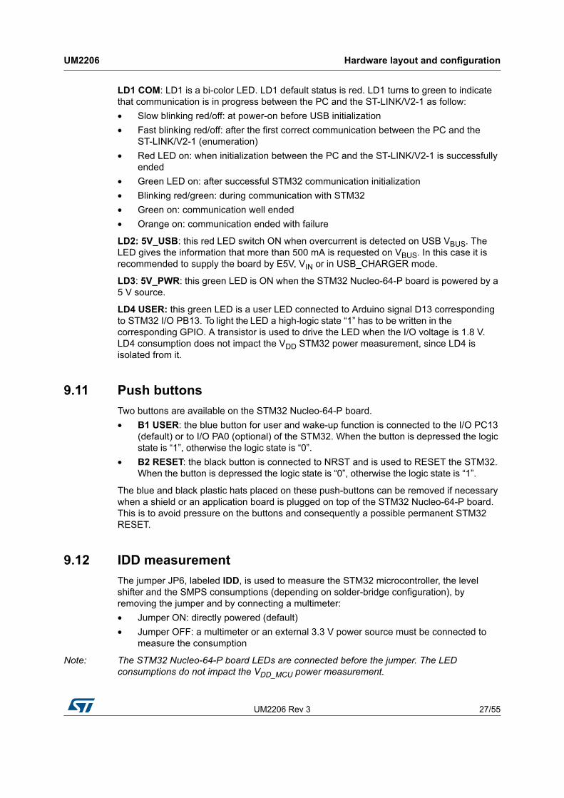
LD1 COM: LD1 is a bi-color LED. LD1 default status is red. LD1 turns to green to indicate that communication is in progress between the PC and the ST-LINK/V2-1 as follow:
• Slow blinking red/off: at power-on before USB initialization
• Fast blinking red/off: after the first correct communication between the PC and the ST-LINK/V2-1 (enumeration)
• Red LED on: when initialization between the PC and the ST-LINK/V2-1 is successfully ended
• Green LED on: after successful STM32 communication initialization
• Blinking red/green: during communication with STM32
• Green on: communication well ended
• Orange on: communication ended with failure
LD2: 5V_USB: this red LED switch ON when overcurrent is detected on USB VBUS. The LED gives the information that more than 500 mA is requested on VBUS. In this case it is recommended to supply the board by E5V, VIN or in USB_CHARGER mode.
LD3: 5V_PWR: this green LED is ON when the STM32 Nucleo-64-P board is powered by a 5 V source.
LD4 USER: this green LED is a user LED connected to Arduino signal D13 corresponding to STM32 I/O PB13. To light the LED a high-logic state “1” has to be written in the corresponding GPIO. A transistor is used to drive the LED when the I/O voltage is 1.8 V. LD4 consumption does not impact the VDD STM32 power measurement, since LD4 is isolated from it.
9.11 Push buttons
Two buttons are available on the STM32 Nucleo-64-P board.
• B1 USER: the blue button for user and wake-up function is connected to the I/O PC13 (default) or to I/O PA0 (optional) of the STM32. When the button is depressed the logic state is “1”, otherwise the logic state is “0”.
• B2 RESET: the black button is connected to NRST and is used to RESET the STM32. When the button is depressed the logic state is “0”, otherwise the logic state is “1”.
The blue and black plastic hats placed on these push-buttons can be removed if necessary when a shield or an application board is plugged on top of the STM32 Nucleo-64-P board. This is to avoid pressure on the buttons and consequently a possible permanent STM32 RESET.
9.12 IDD measurement
The jumper JP6, labeled IDD, is used to measure the STM32 microcontroller, the level shifter and the SMPS consumptions (depending on solder-bridge configuration), by removing the jumper and by connecting a multimeter:
• Jumper ON: directly powered (default)
• Jumper OFF: a multimeter or an external 3.3 V power source must be connected to measure the consumption
Note: The STM32 Nucleo-64-P board LEDs are connected before the jumper. The LED consumptions do not impact the VDD_MCU power measurement.
Hardware layout and configuration UM2206
28/55 UM2206 Rev 3
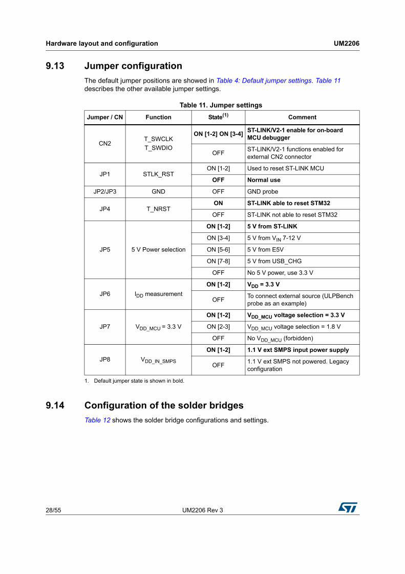
9.13 Jumper configuration
The default jumper positions are showed in Table 4: Default jumper settings. Table 11 describes the other available jumper settings.
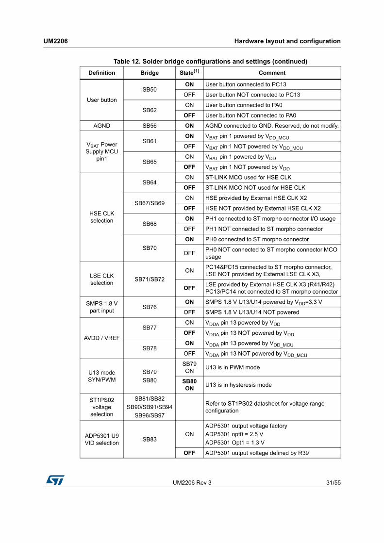
9.14 Configuration of the solder bridges
Table 12 shows the solder bridge configurations and settings.
Table 11. Jumper settings
Jumper / CN Function State(1)
1. Default jumper state is shown in bold.
Comment
CN2T_SWCLK
T_SWDIO
ON [1-2] ON [3-4]ST-LINK/V2-1 enable for on-board MCU debugger
OFFST-LINK/V2-1 functions enabled for external CN2 connector
JP1 STLK_RSTON [1-2] Used to reset ST-LINK MCU
OFF Normal use
JP2/JP3 GND OFF GND probe
JP4 T_NRSTON ST-LINK able to reset STM32
OFF ST-LINK not able to reset STM32
JP5 5 V Power selection
ON [1-2] 5 V from ST-LINK
ON [3-4] 5 V from VIN 7-12 V
ON [5-6] 5 V from E5V
ON [7-8] 5 V from USB_CHG
OFF No 5 V power, use 3.3 V
JP6 IDD measurement
ON [1-2] VDD = 3.3 V
OFF To connect external source (ULPBench probe as an example)
JP7 VDD_MCU = 3.3 V
ON [1-2] VDD_MCU voltage selection = 3.3 V
ON [2-3] VDD_MCU voltage selection = 1.8 V
OFF No VDD_MCU (forbidden)
JP8 VDD_IN_SMPS
ON [1-2] 1.1 V ext SMPS input power supply
OFF1.1 V ext SMPS not powered. Legacy configuration
UM2206 Rev 3 29/55
UM2206 Hardware layout and configuration
54
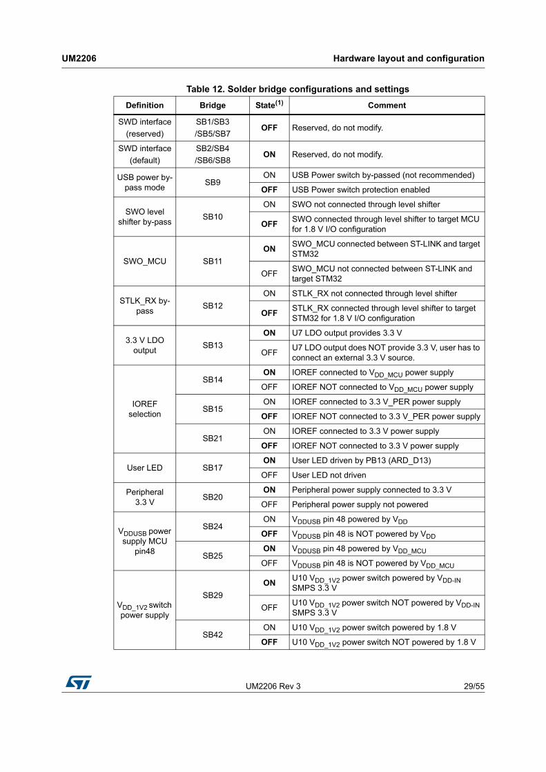
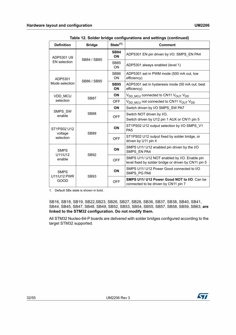
Table 12. Solder bridge configurations and settings
Definition Bridge State(1) Comment
SWD interface
(reserved)
SB1/SB3
/SB5/SB7OFF Reserved, do not modify.
SWD interface
(default)
SB2/SB4
/SB6/SB8ON Reserved, do not modify.
USB power by-pass mode
SB9ON USB Power switch by-passed (not recommended)
OFF USB Power switch protection enabled
SWO level shifter by-pass
SB10
ON SWO not connected through level shifter
OFFSWO connected through level shifter to target MCU for 1.8 V I/O configuration
SWO_MCU SB11
ONSWO_MCU connected between ST-LINK and target STM32
OFFSWO_MCU not connected between ST-LINK and target STM32
STLK_RX by-pass
SB12
ON STLK_RX not connected through level shifter
OFFSTLK_RX connected through level shifter to target STM32 for 1.8 V I/O configuration
3.3 V LDO output
SB13
ON U7 LDO output provides 3.3 V
OFFU7 LDO output does NOT provide 3.3 V, user has to connect an external 3.3 V source.
IOREF selection
SB14ON IOREF connected to VDD_MCU power supply
OFF IOREF NOT connected to VDD_MCU power supply
SB15ON IOREF connected to 3.3 V_PER power supply
OFF IOREF NOT connected to 3.3 V_PER power supply
SB21ON IOREF connected to 3.3 V power supply
OFF IOREF NOT connected to 3.3 V power supply
User LED SB17ON User LED driven by PB13 (ARD_D13)
OFF User LED not driven
Peripheral 3.3 V
SB20ON Peripheral power supply connected to 3.3 V
OFF Peripheral power supply not powered
VDDUSB power supply MCU
pin48
SB24ON VDDUSB pin 48 powered by VDD
OFF VDDUSB pin 48 is NOT powered by VDD
SB25ON VDDUSB pin 48 powered by VDD_MCU
OFF VDDUSB pin 48 is NOT powered by VDD_MCU
VDD_1V2 switch power supply
SB29
ONU10 VDD_1V2 power switch powered by VDD-IN SMPS 3.3 V
OFFU10 VDD_1V2 power switch NOT powered by VDD-IN SMPS 3.3 V
SB42ON U10 VDD_1V2 power switch powered by 1.8 V
OFF U10 VDD_1V2 power switch NOT powered by 1.8 V
Hardware layout and configuration UM2206
30/55 UM2206 Rev 3
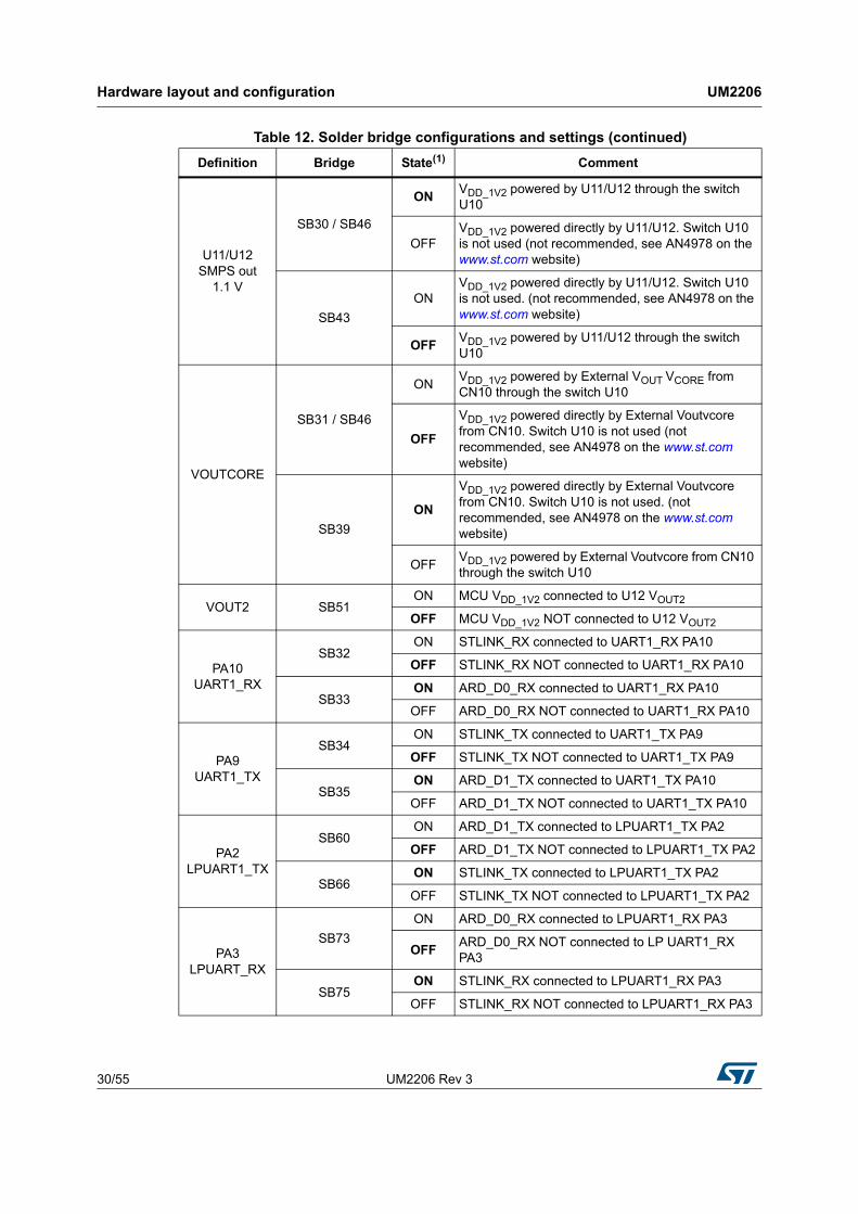
U11/U12 SMPS out
1.1 V
SB30 / SB46
ONVDD_1V2 powered by U11/U12 through the switch U10
OFFVDD_1V2 powered directly by U11/U12. Switch U10 is not used (not recommended, see AN4978 on the www.st.com website)
SB43
ONVDD_1V2 powered directly by U11/U12. Switch U10 is not used. (not recommended, see AN4978 on the www.st.com website)
OFFVDD_1V2 powered by U11/U12 through the switch U10
VOUTCORE
SB31 / SB46
ONVDD_1V2 powered by External VOUT VCORE from CN10 through the switch U10
OFF
VDD_1V2 powered directly by External Voutvcore from CN10. Switch U10 is not used (not recommended, see AN4978 on the www.st.com website)
SB39
ON
VDD_1V2 powered directly by External Voutvcore from CN10. Switch U10 is not used. (not recommended, see AN4978 on the www.st.com website)
OFFVDD_1V2 powered by External Voutvcore from CN10 through the switch U10
VOUT2 SB51ON MCU VDD_1V2 connected to U12 VOUT2
OFF MCU VDD_1V2 NOT connected to U12 VOUT2
PA10 UART1_RX
SB32ON STLINK_RX connected to UART1_RX PA10
OFF STLINK_RX NOT connected to UART1_RX PA10
SB33ON ARD_D0_RX connected to UART1_RX PA10
OFF ARD_D0_RX NOT connected to UART1_RX PA10
PA9 UART1_TX
SB34ON STLINK_TX connected to UART1_TX PA9
OFF STLINK_TX NOT connected to UART1_TX PA9
SB35ON ARD_D1_TX connected to UART1_TX PA10
OFF ARD_D1_TX NOT connected to UART1_TX PA10
PA2 LPUART1_TX
SB60ON ARD_D1_TX connected to LPUART1_TX PA2
OFF ARD_D1_TX NOT connected to LPUART1_TX PA2
SB66ON STLINK_TX connected to LPUART1_TX PA2
OFF STLINK_TX NOT connected to LPUART1_TX PA2
PA3 LPUART_RX
SB73
ON ARD_D0_RX connected to LPUART1_RX PA3
OFFARD_D0_RX NOT connected to LP UART1_RX PA3
SB75ON STLINK_RX connected to LPUART1_RX PA3
OFF STLINK_RX NOT connected to LPUART1_RX PA3
Table 12. Solder bridge configurations and settings (continued)
Definition Bridge State(1) Comment
UM2206 Rev 3 31/55
UM2206 Hardware layout and configuration
54
User button
SB50ON User button connected to PC13
OFF User button NOT connected to PC13
SB62ON User button connected to PA0
OFF User button NOT connected to PA0
AGND SB56 ON AGND connected to GND. Reserved, do not modify.
VBAT Power Supply MCU
pin1
SB61ON VBAT pin 1 powered by VDD_MCU
OFF VBAT pin 1 NOT powered by VDD_MCU
SB65ON VBAT pin 1 powered by VDD
OFF VBAT pin 1 NOT powered by VDD
HSE CLK selection
SB64ON ST-LINK MCO used for HSE CLK
OFF ST-LINK MCO NOT used for HSE CLK
SB67/SB69ON HSE provided by External HSE CLK X2
OFF HSE NOT provided by External HSE CLK X2
SB68ON PH1 connected to ST morpho connector I/O usage
OFF PH1 NOT connected to ST morpho connector
SB70
ON PH0 connected to ST morpho connector
OFFPH0 NOT connected to ST morpho connector MCO usage
LSE CLK selection
SB71/SB72
ONPC14&PC15 connected to ST morpho connector, LSE NOT provided by External LSE CLK X3,
OFFLSE provided by External HSE CLK X3 (R41/R42) PC13/PC14 not connected to ST morpho connector
SMPS 1.8 V part input
SB76ON SMPS 1.8 V U13/U14 powered by VDD=3.3 V
OFF SMPS 1.8 V U13/U14 NOT powered
AVDD / VREF
SB77ON VDDA pin 13 powered by VDD
OFF VDDA pin 13 NOT powered by VDD
SB78ON VDDA pin 13 powered by VDD_MCU
OFF VDDA pin 13 NOT powered by VDD_MCU
U13 mode SYN/PWM
SB79
SB80
SB79 ON
U13 is in PWM mode
SB80 ON
U13 is in hysteresis mode
ST1PS02 voltage
selection
SB81/SB82
SB90/SB91/SB94
SB96/SB97
Refer to ST1PS02 datasheet for voltage range configuration
ADP5301 U9 VID selection
SB83ON
ADP5301 output voltage factory
ADP5301 opt0 = 2.5 V
ADP5301 Opt1 = 1.3 V
OFF ADP5301 output voltage defined by R39
Table 12. Solder bridge configurations and settings (continued)
Definition Bridge State(1) Comment
Hardware layout and configuration UM2206
32/55 UM2206 Rev 3
SB16, SB18, SB19, SB22,SB23, SB26, SB27, SB28, SB36, SB37, SB38, SB40, SB41, SB44, SB45, SB47, SB48, SB49, SB52, SB53, SB54, SB55, SB57, SB58, SB59, SB63, are linked to the STM32 configuration. Do not modify them.
All STM32 Nucleo-64-P boards are delivered with solder bridges configured according to the target STM32 supported.
ADP5301 U9 EN selection
SB84 / SB85
SB84 ON
ADP5301 EN pin driven by I/O: SMPS_EN PA4
SB85 ON
ADP5301 always enabled (level 1)
ADP5301 Mode selection
SB86 / SB95
SB86 ON
ADP5301 set in PWM mode (500 mA out, low efficiency)
SB95 ON
ADP5301 set in hysteresis mode (50 mA out, best efficiency)
VDD_MCU selection
SB87ON VDD_MCU connected to CN11 VOUT VDD
OFF VDD_MCU not connected to CN11 VOUT VDD
SMPS_SW enable
SB88
ON Switch driven by I/O SMPS_SW PA7
OFFSwitch NOT driven by I/O,
Switch driven by U12 pin 1 AUX or CN11 pin 5
ST1PS02 U12 voltage
selectionSB89
ONST1PS02 U12 output selection by I/O SMPS_V1 PA5
OFFST1PS02 U12 output fixed by solder bridge, or driven by U11 pin 4
SMPS U11/U12 enable
SB92
ONSMPS U11/ U12 enabled pin driven by the I/O SMPS_EN PA4
OFFSMPS U11/ U12 NOT enabled by I/O. Enable pin level fixed by solder bridge or driven by CN11 pin 5
SMPS U11/U12 PWR
GOODSB93
ONSMPS U11/ U12 Power Good connected to I/O SMPS_PG PA6
OFFSMPS U11/ U12 Power Good NOT to I/O. Can be connected to be driven by CN11 pin 7
1. Default SBx state is shown in bold.
Table 12. Solder bridge configurations and settings (continued)
Definition Bridge State(1) Comment
UM2206 Rev 3 33/55
UM2206 Connectors
54
10 Connectors
Eight connectors are implemented on the STM32 Nucleo-64-P board:
• CN1: ST-LINK USB connector
• CN7, CN8, CN9 and CN10: Arduino Uno V3 connectors
• CN5 and CN6: ST morpho connectors
• CN11: External SMPS connector
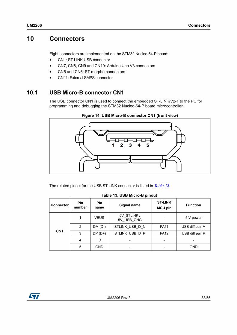
10.1 USB Micro-B connector CN1
The USB connector CN1 is used to connect the embedded ST-LINK/V2-1 to the PC for programming and debugging the STM32 Nucleo-64-P board microcontroller.
Figure 14. USB Micro-B connector CN1 (front view)
The related pinout for the USB ST-LINK connector is listed in Table 13.
Table 13. USB Micro-B pinout
ConnectorPin
numberPin
nameSignal name
ST-LINK
MCU pinFunction
CN1
1 VBUS5V_STLINK /
5V_USB_CHG- 5 V power
2 DM (D-) STLINK_USB_D_N PA11 USB diff pair M
3 DP (D+) STLINK_USB_D_P PA12 USB diff pair P
4 ID - - -
5 GND - - GND
Connectors UM2206
34/55 UM2206 Rev 3
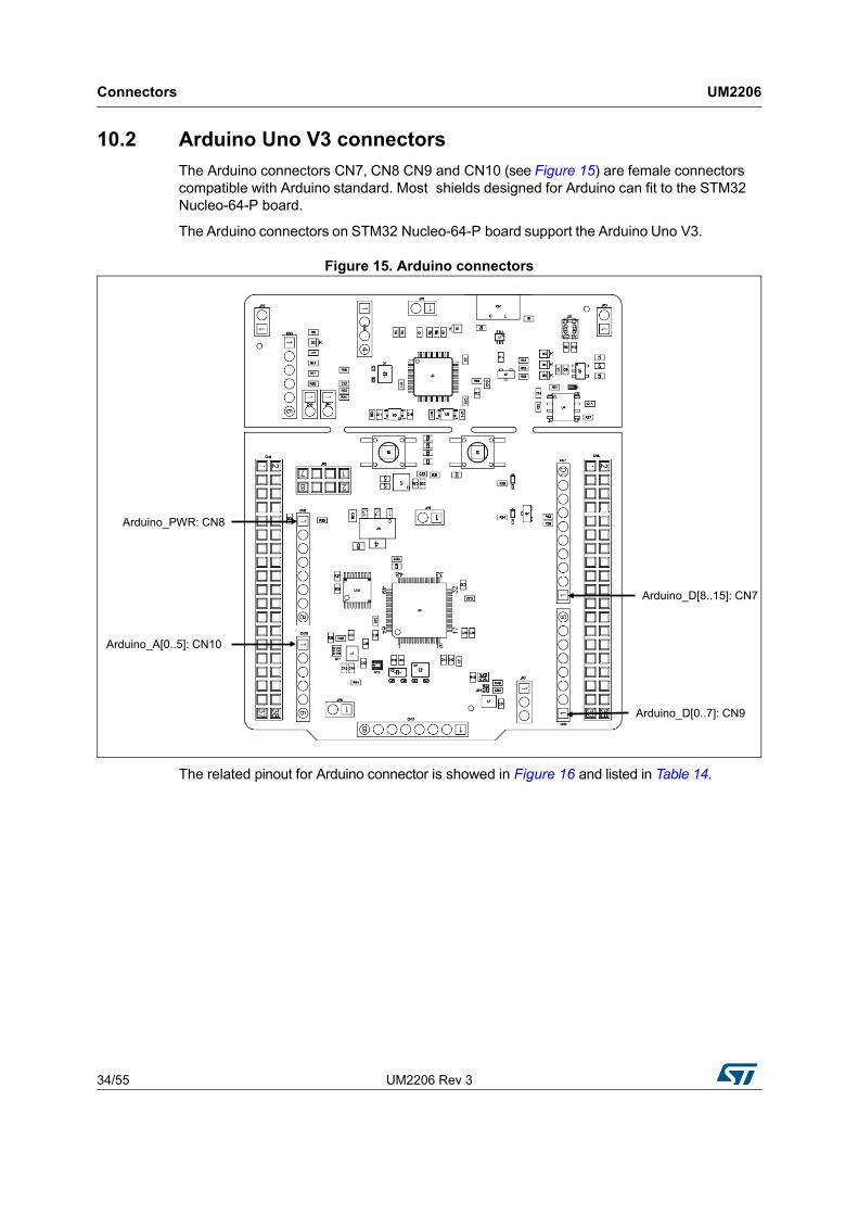
10.2 Arduino Uno V3 connectors
The Arduino connectors CN7, CN8 CN9 and CN10 (see Figure 15) are female connectors compatible with Arduino standard. Most shields designed for Arduino can fit to the STM32 Nucleo-64-P board.
The Arduino connectors on STM32 Nucleo-64-P board support the Arduino Uno V3.
Figure 15. Arduino connectors
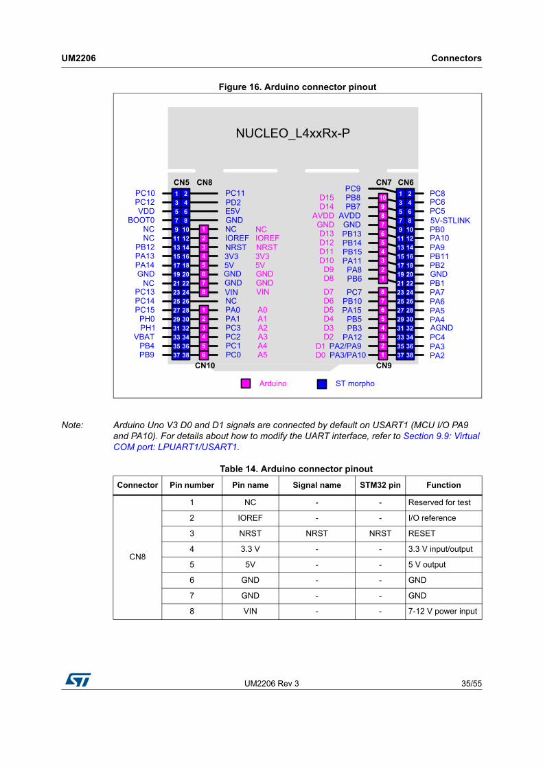
The related pinout for Arduino connector is showed in Figure 16 and listed in Table 14.
Arduino_D[8..15]: CN7
Arduino_D[0..7]: CN9
Arduino_A[0..5]: CN10
Arduino_PWR: CN8
UM2206 Rev 3 35/55
UM2206 Connectors
54
Figure 16. Arduino connector pinout
Note: Arduino Uno V3 D0 and D1 signals are connected by default on USART1 (MCU I/O PA9 and PA10). For details about how to modify the UART interface, refer to Section 9.9: Virtual COM port: LPUART1/USART1.
PC0PC1PC2PC3PA1PA0NCVINGNDGND5V3V3NRSTIOREFNCGNDE5VPD2PC11
PB9PB4
VBATPH1PH0
PC15PC14PC13
NCGNDPA14PA13PB12
NCNC
BOOT0VDD
PC12
NUCLEO_L4xxRx-P
PA2PA3PC4AGNDPA4PA5PA6PA7PB1GNDPB2PB11PA9PA10PB05V-STLINKPC5PC6PC8
PB6PA8
PA11PB15PB14PB13GND
AVDDPB7PB8PC9
PA3/PA10PA2/PA9
PA12PB3PB5
PA15PB10PC7
D8D9
D10D11D12D13
GNDAVDD
D14D15
D0D1
D2D3D4D5D6D7
A5A4A3A2A1A0
VINGNDGND5V3V3NRSTIOREFNC
Arduino orpho
PC10 10987654321
87654321
13579
1113151719212325272931333537
2468
101214161820222426283032343638
123456
12345678
13579
1113151719212325272931333537
2468
101214161820222426283032343638
CN5 CN6CN7
CN9
CN8
CN10
Table 14. Arduino connector pinout
Connector Pin number Pin name Signal name STM32 pin Function
CN8
1 NC - - Reserved for test
2 IOREF - - I/O reference
3 NRST NRST NRST RESET
4 3.3 V - - 3.3 V input/output
5 5V - - 5 V output
6 GND - - GND
7 GND - - GND
8 VIN - - 7-12 V power input
Connectors UM2206
36/55 UM2206 Rev 3
CN10
1 A0 ADC PA0 ADC1_IN5
2 A1 ADC PA1 ADC1_IN6
3 A2 ADC PC3 ADC1_IN4
4 A3 ADC PC2 ADC1_IN3
5 A4 ADC PC1ADC1_IN2/I2C3_
SDA
6 A5 ADC PC0ADC1_IN1/I2C3_
SCL
CN7
10 SCL/D15 ARD_D15 PB8 I2C1_SCL
9 SDA/D14 ARD_D14 PB7 I2C1_SDA
8 AVDD VREF - VREF
7 GND - - Ground
6 SCK/D13 ARD_D13 PB13 SPI2_SCK
5 MISO/D12 ARD_D12 PB14 SPI2_MISO
4PWM/MOSI/
D11ARD_D11 PB15
TIM15_CH2/SPI2_MOSI
3 PWM/CS/D10 ARD_D10 PA11TIM1_CH4/SPIx_
NSS
2 PWM/D9 ARD_D9 PA8 TIM1_CH1
1 D8 ARD_D8 PB6 IO
CN9
8 D7 ARD_D7 PC7 IO
7 PWM/D6 ARD_D6 PB10 TIM2_CH3
6 PWM/D5 ARD_D5 PA15 TIM2_CH1
5 D4 ARD_D4 PB5 EXT_IT_5
4 PWM/D3 ARD_D3 PB3 TIM2_CH2
3 D2 ARD_D2 PA12 IO
2 TX/D1 ARD_D1PA2 /
PA9LPUSART1_TX /
USART1_TX
1 RX/D0 ARD_D0PA3 /
PA10LPUSART1_RX /
USART1_RX
Table 14. Arduino connector pinout (continued)
Connector Pin number Pin name Signal name STM32 pin Function
UM2206 Rev 3 37/55
UM2206 Connectors
54
10.3 ST morpho connectors CN5 and CN6
The ST morpho connectors CN5 and CN6 are male pin headers accessible on both sides of the STM32 Nucleo-64-P board (see Figure 17). All signals and power pins, except VDD_CORE 1.2 V of the STM32, are available on the ST morpho connectors. These connectors can also be probed by an oscilloscope, logical analyzer or voltmeter.
Figure 17. ST morpho connector
The related pinout and the MCU assignment for the ST morpho connector are listed in Figure 18.
:CN6
: CN5
Connectors UM2206
38/55 UM2206 Rev 3
Figure 18. ST morpho connector pinout
Note: Arduino Uno V3 D0 and D1 signals are connected by default on USART1 (MCU I/O PA9 and PA10). Refer to Section 9.9: Virtual COM port: LPUART1/USART1 for details about UART interface modification.
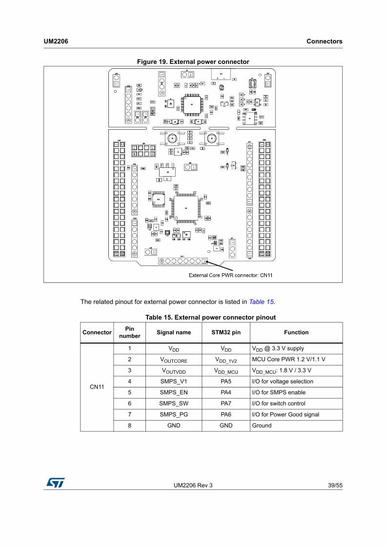
10.4 External power connector
The external power connector CN11 is an 8-pin, single-row, 2.54 mm-pitch connector. By default this connector is not soldered. The PCB footprint gives the possibility to easily control the Vcore logic and the VDD_MCU power supply with an external source. The external power connector is showed in Figure 19.
PC0PC1PC2PC3PA1PA0NCVINGNDGND5V3V3NRSTIOREFNCGNDE5VPD2PC11
PB9PB4
VBATPH1PH0
PC15PC14PC13
NCGNDPA14PA13PB12
NCNC
BOOT0VDD
PC12
NUCLEO_L4xxRx-P
PA2PA3PC4AGNDPA4PA5PA6PA7PB1GNDPB2PB11PA9PA10PB05V-STLINKPC5PC6PC8
PB6PA8
PA11PB15PB14PB13GND
AVDDPB7PB8PC9
PA3/PA10PA2/PA9
PA12PB3PB5
PA15PB10PC7
D8D9
D10D11D12D13
GNDAVDD
D14D15
D0D1
D2D3D4D5D6D7
A5A4A3A2A1A0
VINGNDGND5V3V3NRSTIOREFNC
Arduino orpho
PC10 10987654321
87654321
13579
1113151719212325272931333537
2468
101214161820222426283032343638
123456
12345678
13579
1113151719212325272931333537
2468
101214161820222426283032343638
CN5 CN6CN7
CN9
CN8
CN10
UM2206 Rev 3 39/55
UM2206 Connectors
54
Figure 19. External power connector
The related pinout for external power connector is listed in Table 15.
Table 15. External power connector pinout
ConnectorPin
numberSignal name STM32 pin Function
CN11
1 VDD VDD VDD @ 3.3 V supply
2 VOUTCORE VDD_1V2 MCU Core PWR 1.2 V/1.1 V
3 VOUTVDD VDD_MCU VDD_MCU: 1.8 V / 3.3 V
4 SMPS_V1 PA5 I/O for voltage selection
5 SMPS_EN PA4 I/O for SMPS enable
6 SMPS_SW PA7 I/O for switch control
7 SMPS_PG PA6 I/O for Power Good signal
8 GND GND Ground
NUCLEO-L412RB-P, NUCLEO-L433RC-P and NUCLEO-L452RE-P I/O assignment UM2206
40/55 UM2206 Rev 3
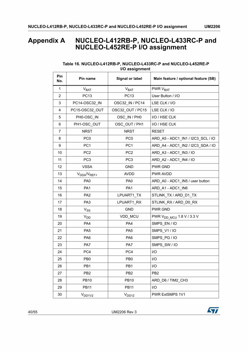
Appendix A NUCLEO-L412RB-P, NUCLEO-L433RC-P and NUCLEO-L452RE-P I/O assignment
Table 16. NUCLEO-L412RB-P, NUCLEO-L433RC-P and NUCLEO-L452RE-P I/O assignment
Pin No.
Pin name Signal or label Main feature / optional feature (SB)
1 VBAT VBAT PWR VBAT
2 PC13 PC13 User Button / I/O
3 PC14-OSC32_IN OSC32_IN / PC14 LSE CLK / I/O
4 PC15-OSC32_OUT OSC32_OUT / PC15 LSE CLK / IO
5 PH0-OSC_IN OSC_IN / PH0 I/O / HSE CLK
6 PH1-OSC_OUT OSC_OUT / PH1 I/O / HSE CLK
7 NRST NRST RESET
8 PC0 PC0 ARD_A5 - ADC1_IN1 / I2C3_SCL / IO
9 PC1 PC1 ARD_A4 - ADC1_IN2 / I2C3_SDA / IO
10 PC2 PC2 ARD_A3 - ADC1_IN3 / IO
11 PC3 PC3 ARD_A2 - ADC1_IN4 / IO
12 VSSA GND PWR GND
13 VDDA/VREF+ AVDD PWR AVDD
14 PA0 PA0 ARD_A0 - ADC1_IN5 / user button
15 PA1 PA1 ARD_A1 - ADC1_IN6
16 PA2 LPUART1_TX STLINK_TX / ARD_D1_TX
17 PA3 LPUART1_RX STLINK_RX / ARD_D0_RX
18 VSS GND PWR GND
19 VDD VDD_MCU PWR VDD_MCU 1.8 V / 3.3 V
20 PA4 PA4 SMPS_EN / IO
21 PA5 PA5 SMPS_V1 / IO
22 PA6 PA6 SMPS_PG / IO
23 PA7 PA7 SMPS_SW / IO
24 PC4 PC4 I/O
25 PB0 PB0 I/O
26 PB1 PB1 I/O
27 PB2 PB2 PB2
28 PB10 PB10 ARD_D6 / TIM2_CH3
29 PB11 PB11 I/O
30 VDD1V2 VDD12 PWR ExtSMPS 1V1
UM2206 Rev 3 41/55
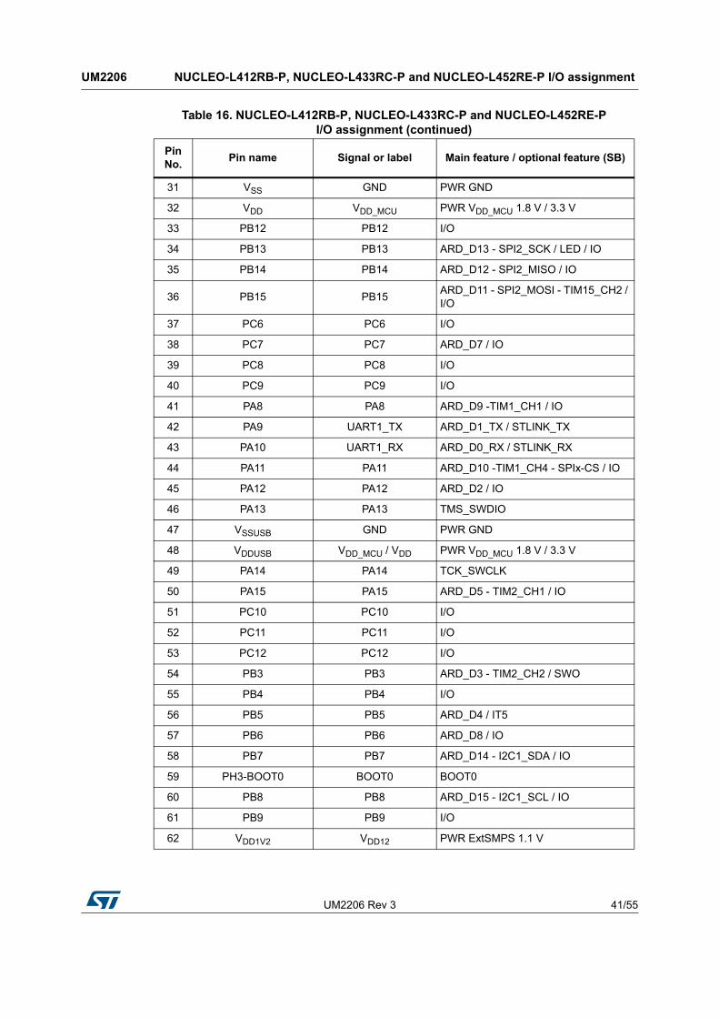
UM2206 NUCLEO-L412RB-P, NUCLEO-L433RC-P and NUCLEO-L452RE-P I/O assignment
54
31 VSS GND PWR GND
32 VDD VDD_MCU PWR VDD_MCU 1.8 V / 3.3 V
33 PB12 PB12 I/O
34 PB13 PB13 ARD_D13 - SPI2_SCK / LED / IO
35 PB14 PB14 ARD_D12 - SPI2_MISO / IO
36 PB15 PB15ARD_D11 - SPI2_MOSI - TIM15_CH2 / I/O
37 PC6 PC6 I/O
38 PC7 PC7 ARD_D7 / IO
39 PC8 PC8 I/O
40 PC9 PC9 I/O
41 PA8 PA8 ARD_D9 -TIM1_CH1 / IO
42 PA9 UART1_TX ARD_D1_TX / STLINK_TX
43 PA10 UART1_RX ARD_D0_RX / STLINK_RX
44 PA11 PA11 ARD_D10 -TIM1_CH4 - SPIx-CS / IO
45 PA12 PA12 ARD_D2 / IO
46 PA13 PA13 TMS_SWDIO
47 VSSUSB GND PWR GND
48 VDDUSB VDD_MCU / VDD PWR VDD_MCU 1.8 V / 3.3 V
49 PA14 PA14 TCK_SWCLK
50 PA15 PA15 ARD_D5 - TIM2_CH1 / IO
51 PC10 PC10 I/O
52 PC11 PC11 I/O
53 PC12 PC12 I/O
54 PB3 PB3 ARD_D3 - TIM2_CH2 / SWO
55 PB4 PB4 I/O
56 PB5 PB5 ARD_D4 / IT5
57 PB6 PB6 ARD_D8 / IO
58 PB7 PB7 ARD_D14 - I2C1_SDA / IO
59 PH3-BOOT0 BOOT0 BOOT0
60 PB8 PB8 ARD_D15 - I2C1_SCL / IO
61 PB9 PB9 I/O
62 VDD1V2 VDD12 PWR ExtSMPS 1.1 V
Table 16. NUCLEO-L412RB-P, NUCLEO-L433RC-P and NUCLEO-L452RE-P I/O assignment (continued)
Pin No.
Pin name Signal or label Main feature / optional feature (SB)
NUCLEO-L412RB-P, NUCLEO-L433RC-P and NUCLEO-L452RE-P I/O assignment UM2206
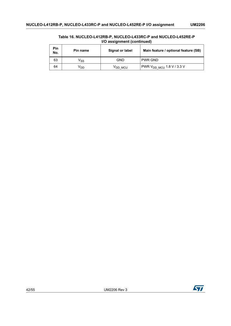
42/55 UM2206 Rev 3
63 VSS GND PWR GND
64 VDD VDD_MCU PWR VDD_MCU 1.8 V / 3.3 V
Table 16. NUCLEO-L412RB-P, NUCLEO-L433RC-P and NUCLEO-L452RE-P I/O assignment (continued)
Pin No.
Pin name Signal or label Main feature / optional feature (SB)
UM2206 Rev 3 43/55
UM2206 Electrical schematics
54
Appendix B Electrical schematics
This section provides the design schematics for the STM32 Nucleo-64-P board features:
• MB1319:
– Top and Power (see Figure 20)
– STM32 I/Os (see Figure 21)
– STM32 Power (see Figure 22)
– Arduino extension connectors (see Figure 23)
– Main Power 5 V and 3.3 V (see Figure 24)
– STM32 power SMPS (see Figure 25)
– ST-LINK/V2-1 (see Figure 26)
Elec
trical s
ch
em
atic
sU
M2
206
44/5
5U
M2
206 R
ev 3
Figure 20. Top and Power
2 8
mb1319 Top: hierarchical viewTitle:
Size:Reference:Sheet: ofA4
Revision:
Project: NUCLEO64 ext-SMPS
MB1319C 0105-January-2018
L412RB_P
Date:-
Variant:
MB1319C-01 xxxx
BOARD REF
HW101
PA[0..15]
PB[0..15]
PC[0..15]
PH[0..1]
Cuttable part on PCB
PA[0..15]
PB[0..15]
PC[0..15]
PD2BOOT0
PH[0..1]
ARD_D0_RXARD_D1_TX
NRST
MCO
STLINK_TX
TMS_SWDIO
STLINK_RX
SWO
TCK_SWCLK
U_STM32_microcontroller_IOsSTM32_microcontroller_IOs.SchDoc
U_STM32_microcontroller_powerSTM32_microcontroller_power.SchDoc
PA[0..15]
PB[0..15]
PC[0..15]
PD2
NRST
BOOT0
PH[0..1]
ARD_D0_RXARD_D1_TX
U_Arduino_extension_connectorsArduino_extension_connectors.SchDoc
U_PowerPower.SchDoc
PA[0..15]
NRST
U_Power SMPSPower SMPS.SchDoc
STLINK_TX
TMS_SWDIOSWO
STLINK_RX
MCO
NRST
TCK_SWCLK
U_ST_LINK_V2-1ST_LINK_V2-1.SchDoc
NUCLEO-L412RB-P
BOARD CPN
HW102
MB1319C
PCB
HW100
LOGO ST
HW105
DNF
LOGO CE
HW106
DNF
LOGO ESD
HW107
DNF
LOGO ROHS
HW108
DNF
LOGO STM32
HW109
DNF
BLISTER
NUCLEO64_BLISTER
HW103
LOGO NUCLEO
HW104
DNF
UM
22
06E
lectrica
l sc
he
ma
tics
UM
2206
Re
v 345
/55
Figure 21. STM32 I/Os
3 8
STM32 microcontroller I/OsTitle:
Size:Reference:Sheet: ofA4
Revision:
Project: NUCLEO64 ext-SMPS
MB1319C 0105-January-2018
L412RB_P
Date:-
Variant:
PA4PA5PA6PA7
PA11PA12
PA9PA10
PA0PA1
PA15
PA3
PA13PA14
PA2
PA8
PB5
PB6
PB7
PB14
PB15
PB8
PB9
PB1
PB2
PB3
PB0
PB4
PB12
PB13
PC0PC1PC2PC3PC4
PC6PC7PC8PC9PC10PC11PC12PC13
PC14PC15
A0A1
A2A3A4A5
D12
D11
D13
D14
D15
NRST
VDD_MCU
PA[0..15]PA[0..15] PB[0..15]PB[0..15] PC[0..15]PC[0..15]
PD2PD2
BOOT0
D2
D4
D3/SWO
D5
D7
D8
D9
D10
SB52
SB50
NX3215SA-32.768KX3
0RR42
0RR41
1K
R30
100KR28
NX3225GD-8.00M
12
X2DNF
10K
R32
1K
R31
SB63
SB44
SB18SB16 DNF
SB22
SB26
SB19 DNF
SB23 DNF
SB28SB27 DNF
SB38SB36 DNF
SB53SB55 DNFSB58
SB54SB40 DNF
SB49 DNF
SB48 DNF
PB10
PB11
SB41 DNF
NRST
SW_BLUE1
3 42
B1
100nFC21
SW_BLACK
134
2
B2
RESET FUNCTION
USER BUTTON
PH0PH1
EXTERNAL HSE CLK
B_USER
EXTERNAL LSE CLK
SB47 DNF
SB37
SB70SB68
OSC_IN
OSC_OUT
PH[0..1] PH[0..1]
SB72 DNF
OSC32_IN
OSC32_OUT
SB71 DNF
D6
SB62DNF
PC13
PA0
8.2pF
C47DNF
8.2pF
C48DNF
SB59 DNF
SB45
SB75
SB66
SB32DNF
SB34DNF
UART1_RXUART1_TX
LPUART1_TXLPUART1_RXSTLINK_RX
STLINK_TX
STLINK_RX
STLINK_TX
SB33
SB60DNF
SB35
SB73DNFARD_D0_RX
ARD_D1_TX
ARD_D1_TX
ARD_D0_RXARD_D0_RX
ARD_D1_TX
SB57 DNF
For IC compatible config 1:Pin25: PB0: SB63Pin26: PB1: SB52Pin27: PB2: SB44Pin54: PB3: SB18Pin55: PB4: SB22Pin56: PB5: SB26Pin57: PB6: SB28Pin58: PB7: SB38Pin60: PB8: SB53Pin61: PB9: SB58Pin28: PB10: SB54Pin29: PB11: SB37Pin59: PH3-BOOT0: SB45
PC5
PB2
TMS/SWDIO
PB7BOOT0
BOOT0
SB69 DNF
SB67 DNF
STLINK_TX
STLINK_RX
TCK_SWCLK
SWO
MCO
For IC compatible config 2:Pin25: PC5: SB59Pin26: PB0: SB57Pin27: PB1: SB47Pin54: PD2: SB16Pin55: PB3: SB19Pin56: PB4: SB23Pin57: PB5: SB27Pin58: PB6: SB36Pin60: PH3-BOOT0: SB48Pin61: PB8: SB55Pin28: PB2: SB40Pin29: PB10: SB49Pin59: PB7: SB41
TCK/SWCLKTMS_SWDIO
SB64 DNF
PC132
PC14 - OSC32_IN3
PC15 - OSC32_OUT4
PC08
PC19
PC210
PC311
PA014
PA115
PA216
PA317
PA420
PA521
PA622
PA723
PC424
PB0 25
PB1 26
PB2 27
PB10 28
PB11 29
PB12 33
PB13 34
PB14 35
PB15 36
PC637
PC738
PC839
PC940
PA841
PA942
PA1043
PA1144
PA1245
PA1346
PA1449
PA1550
PC1051
PC1152
PC1253
PB4 55
PB5 56
PB6 57
PB7 58
PB9 61
PB3 54
PH3-BOOT0 59
PB8 60
MCU CLK & RST
MCU_IOs
PH0 - OSC_IN5
PH1 - OSC_OUT6
NRST 7
STM32L412RBT6P
U9A
10pFC20
10pFC22
BLACK HAT
HW18
BLUE HAT
HW17
22nFC23
6.8pF
C45
6.8pF
C46Part above should beclosed to MCU
Elec
trical s
ch
em
atic
sU
M2
206
46/5
5U
M2
206 R
ev 3
Figure 22. STM32 Power
4 8
STM32 microcontroller PowerTitle:
Size:Reference:Sheet: ofA4
Revision:
Project: NUCLEO64 ext-SMPS
MB1319C 0105-January-2018
L412RB_P
Date:-
Variant:
VDD_MCU
VDD
AVDD
AGND
AVDD
AGND
VDD
VBAT
AGND
SB61
SB74DNF
SB77DNFSB78
SB56
SB65DNFVDD_MCU
VDD_MCU
VDD_MCU
VDD
VDDUSB
100nFC35
100nFC31
100nFC32
100nFC38
100nFC41
1uFC39
VBAT
DECAPS
SB24DNFSB25
1uFC40
VDDUSB
1uFC30
4.7uFC36
Ceramic capacitor (Low ESR, ESR<1ohm)
VDD_1V2
1nFC34
1nFC33
VDD_1V2
SB74 use to bypass L2 when Nucleo powered by Arduino AVDD
VBAT1
VSSA/VREF- 12VDDA/VREF+13
VSS_4 18VDD_419
VSS_1 31VDD_132
VSS_2 47VDDUSB48
VSS_3 63VDD_364
MCU_PWR
VDD1262 VDD1230
STM32L412RBT6P
U9B
600R@100MHzL2
MCU PWR SUPPLIES
UM
22
06E
lectrica
l sc
he
ma
tics
UM
2206
Re
v 347
/55
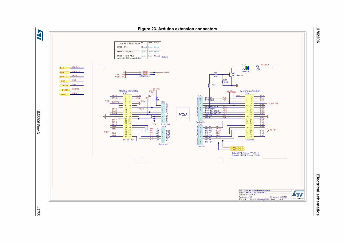
Figure 23. Arduino extension connectors
5 8
Arduino extension connectorsTitle:
Size:Reference:Sheet: ofA4
Revision:
Project: NUCLEO64 ext-SMPS
MB1319C 0105-January-2018
L412RB_P
Date:-
Variant:
IOREF
5V
A0A1A2A3A4A5
D0_RXD1_TXD2_IO
D4_ITD3_TIM
D5_TIMD6_TIMD7_IO
D8_IOD9_TIMD10_TIM_SPI_CS
D14_SDAD15_SCL
PA0PA4PA5PA6PA7
PA12
PB0
PB1
PB3PB4
PB8PB7
PA11
PA1 PA15
PA13PA14
PA8
PC0PC1PC2PC3
PC4
PC5PC6
PC7
PB5
PB6
PB14PB15
PB2PB11
PB12PB13
PC8PC9PC10 PC11PC12
PC13PC14PC15
PB10
NRST
VIN
PD2
PA[0..15]PA[0..15]
PB[0..15]PB[0..15]
PC[0..15]PC[0..15]
PD2 PD2
AGND
NRST NRST
AVDD
5V_STLINKVDD BOOT0
BOOT0 BOOT0
D13_SPI_SCKD12_MISOD11_TIM_MOSI
MCU Ardu
ino
Con
nect
orAr
duin
oC
onne
ctor
Ardu
ino
Con
nect
orA
rdui
noC
onne
ctor
E5V
Morpho connector Morpho connector
VBAT
510R
R34
SB17
Socket 6x1
123456
CN10
Socket 8x1
12345678
CN9Socket 8x1
12345678
CN8
Socket 10x1
123456789
10
CN7
Header 19x2
1 23 45791113151719
68
101214161820
212325272931333537
222426283032343638
CN5
Header 19x2
1 23 45791113151719
68
101214161820
212325272931333537
222426283032343638
CN6
PH1PH0
PH[0..1] PH[0..1]
PA9PA10
PA3PA2PB9
SB21DNFSB15DNFSB14
IOREF
3V3
3V33V3_PER
VDD_MCU
3V3_PER
GREEN
LD4
IOREF SELECTIONIOREF= 3V3
IOREF = 3V3_PER
IOREF = VDD_MCU
SB21 SB15 SB14
Closed Open Open
Open Open
Open Open
Closed
ClosedMainly for 1V8 compatibility
1KR35
5V_VIN
ARD_D0_RXARD_D1_TX
Default
47K
R36
3
1
2
9013-SOT23Q2
100KR33
Default UART1 from PA9/PA10Optional: LPUART1 from PA2/PA3
Elec
trical s
ch
em
atic
sU
M2
206
48/5
5U
M2
206 R
ev 3
Figure 24. Main Power 5 V, 3.3 V
6 8
MAIN POWER 5V / 3V3Title:
Size:Reference:Sheet: ofA4
Revision:
Project: NUCLEO64 ext-SMPS
MB1319C 0105-January-2018
L412RB_P
Date:-
Variant:
3V3
VIN
5V VDD
5V_VIN
10uFC28
LD1117S50TR
Vin3 Vout 2
Gnd
1
Tab 4
U8
10uFC29
LD39050PU33R
EN1
GN
D2
PG 3VIN6
NC 5
VOUT 4
GN
DEP
U7
SB13
HW6
HW5
5V
510RR29E5V
SB20 3V3_PER
GREENLD3
1uFC26
100nFC25
100nFC24
1uFC27
JP6
5V PWR SELECTION
3V3 PWR
5V_STLINK_SW
VIN / 5V PWR
5V_USB_CHG
5V_VIN
E5V from ST-Morpho connector5V_USB_CHG from USB-STLINK CONNECTOR
JP6 for IDD Measurement
1 23 45 67 8
Jumper_Header_4x2
JP5
UM
22
06E
lectrica
l sc
he
ma
tics
UM
2206
Re
v 349
/55
Figure 25. STM32 power SMPS
7 8
STM32 Power SMPSTitle:
Size:Reference:Sheet: ofA3
Revision:
Project: NUCLEO64 ext-SMPS
MB1319C 0105-January-2018
L412RB_P
Date:-
Variant:
SMPS_V
1SM
PS_EN
SMPS_PG
SMPS_SW
VO
UTV
DD
U13 AND U14 ARE EXCLUSIVELY POPULATED
VDD
VDD_1V2
VDD
VDD_MCU
SB76
SB79 DNFSB80
SB87
SB89
SB92
SB93
SB29
SB86 DNFSB95
SB83DNF
SB90 DNF
SB91 DNF
SB94 DNF
SB82 DNF
SB81 DNF
0RR44
DNF
SB31 DNFSB46
SB39
SB30
SB51 DNF
10uFC49
10uFC51100nF
C50
ST1PS01EJR
ENB2 SW C3
VINA3 PG E1
VOUT E3
D1A1
D0C1
GND D2
U14
DNF
VDD_SMPS_1V8
ADP5301ACBZ-2-R7
ENA3 SW A1PVINA2
PGNDB1
FB C2
VID C3SYNC/MODEB3
VOUTOK C1AGNDB2
U13
SMPS_PGST1PS02D1QTR
EN12 SW 3
VIN2 PG 7
VOUT 5
D110
D09
GN
D4
D211
CL8
VOUT2 6
AUX 1
U12
DNF
2.2uH 2.6A 0.100R
L3
2.2uH 2.6A 0.100R
L1
SB42DNF
VDD_IN_SMPS
VDD_SMPS_1V8
SB88
SMPS_V1
SMPS_EN
SMPS_PG
SMPS_SW
VOUTVDD
VOUTVDD
VDD
SB76: DEFAULT: OPENClosed: when VDD_MCU is provided from U13 or U14Open: when VDD_MCU is provided from VDD or CN11
VDD_MCU tableVDD_MCU= VDD
VDD_MCU = 1V8
VDD_MCU = VOUTVDD
JP7 SB87
Open
Open
Open
[3-2]
Closed
SYNC/MODE tablePWM MODE
HYSTERESIS MODE
SB79 SB80
Closed Open
Open Closed
U11 AND U12 ARE EXCLUSIVELY POPULATED VDD_1V2 table SB46 SB51 SB39
Closed Open Open
Open Open
Open Open
Closed
Closed
Comment on this part are for Ext 1V2 SMPS configuration
Header 8x1
2 1345678
CN11
DNF
ST1PS02D MODEV DEFAULT
V Middle
V HIGH
SB91 SB90 SB82
OpenOpen
Open
Open
Closed
Closed
SB94
Open
SB81
Open
Closed
VOUT
1V10
1V15
Open ClosedClosed
Closed
OpenOpen 1V20
D0 D1
19K6R43
1M
R40DNF
10uFC44 10uF
C37
100nFC43
PA[0..15]PA[0..15]
PA4
PA5
PA6
PA7
SB85 DNFSB84
SMPS_SW
VO
UTC
OR
E
VOUTCORE
10uFC42DNF
VDD_SMPS_1V2
SB43 DNFVDD_SMPS_1V2
SB43
Closed Open Open Open
Open
Open
Open
330RR38
NRST
3M3R37
HW8
JP8 VDD_IN_SMPS
VDD_1V2_SW
VOUT2
VOUTCORE
Header 3x1
21
3
JP7
HW7[1-2]
TS3A44159PWR
COM114
COM22
IN1-216
COM36
COM410
NC1 15NO1 13
NC2 3NO2 1
NC3 7NO3 5
NC4 11NO4 9
VCC12 GND 4
IN3-48
U10
Default
JP7[1-2]: NO SMPS SELECTION, VDD = VDD_MCU
JP7[3-2]: SMPS SELECTION, VDD_MCU = 1V8
EXTERNAL SMPS SELECTION: VDD_MCU = FROM CN11
Default: JP7[1-2]
JP8 selection: DEFAULT: CLOSEDClosed to select 1V2 power DefaultOpen for legacy configuration
Opt0: Rvid= 19.6K VOUT= 1V8
Opt1: Rvid= 25.5K VOUT= 1V1
SB83: DEFAULT OPENclosed: VID Short to PVIN:ADP5301 Opt1: VOUT=1V3
VDD_1V2 from U11 or U12 wo SW
VDD_1V2 from U11 or U12 or CN11+SW
VDD_1V2 from U12 VOUT2
VDD_1V2 from CN11 VOUTCORE wo SW
SB30: DEFAULT CLOSEDClosed:If ADI5301 is used or ST1PS02 VOUT is usedOpen: If ST1PS02 VOUT2 is used, or Ext SMPS on CN11
SB31: DEFAULT OPENOpen: when SB30 is closedClosed: If using ExternalSMPS on CN11 and U8 isneeded
EXTERNAL SMPS SELECTION VOUTCORE FROM CN11
Default
EXTERNAL SMPS SELECTION FROM CN11
ENA3 SW A1PVINA2
PGNDB1
FB C2
VID C3SYNC/MODEB3
VOUTOK C1AGNDB2
ADP5301ACBZ-3-R7U11
25K5R39
SB96 DNFSB97 DNF
SB96 SB97
D2
VDD_MCU_SELECTION
SMPS SELECTION, VDD_1V2
ClosedOpen0 0 0
Open Closed
Open Closed0
0
1 0
0 1
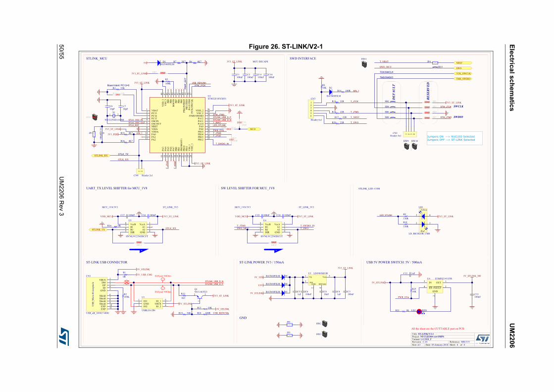
Elec
trical s
ch
em
atic
sU
M2
206
50/5
5U
M2
206 R
ev 3
Figure 26. ST-LINK/V2-1
8 8
ST-LINK/V2-1Title:
Size:Reference:Sheet: ofA3
Revision:
Project: NUCLEO64 ext-SMPS
MB1319C 0105-January-2018
L412RB_P
Date:-
Variant:
STLINK_USB_D_NSTLINK_USB_D_P
STLK_RST
T_JT
CK
T_JTCKT_JTMS
STM_JTMS
STM_JTCK
STLK_OSC_INSTLK_OSC_OUT
T_N
RS
T
AIN_1
5V_STLINK
Jumpers ON --> NUCLEO SelectedJumpers OFF --> ST-LINK Selected
Board Ident: PC13=0
T_JTCK
T_JTMS
STM_JTMS
STM_JTCK SWCLK
SWDIO
RESERVED
DEFAULT
T_SWDIO_IN
LED_STLINK
LED_STLINK
AIN_1
STLINK_USB_D_NSTLINK_USB_D_P
T_SWO
5V_STLINK
USB_RENUMn
USB_RENUMn
3V3_ST_LINK
3V3_ST_LINK
3V3_ST_LINK3V3_ST_LINK
3V3_ST_LINK
3V3_ST_LINK
3V3_ST_LINK
PWR_EXT
3V3_ST_LINK
3V3_PER
3V3_ST_LINK
5V_STLINK
3V3_ST_LINK
5V_VIN
5V 4K7R62K7R7
100K
R5
10KR4
10KR3DNF
NX3225GD-8.00M
1 2X1
10pFC9
10pFC7
4K7R24
4K7R22
100RR23
DNF
100R R19DNF
USB_uB_105017-0001
VBUS 1
DM 2
DP 3
ID 4
GND 5
Shield 6
USB
_Mic
ro-B
rece
ptac
le
Shield 7
Shield 8
Shield 9
EXP 10
EXP 11
CN1
1K5
R12100KR2
10KR13
100RR1836KR15
330R
R10330R
R9
BAT60JFILM D3
BAT60JFILM D5
1uFC5
100nFC6
10nFC8
BAT60JFILM
D210KR8
100RR16
22RR11
22RR17
22RR20
22RR14
SB1DNF
SB3DNF
SB5DNF
SB7DNF
SB2
SB4
SB6
SB8
LD3985M33R51
2
GND3
4
BYPASSINH
Vin Vout
U3
STM32F103CBT6
VBAT1
PA7
17
PC132
PA12 33PC143
PB0
18
PC154 JTMS/SWDIO 34
OSCIN5
PB1
19
OSCOUT6
VSS_2 35
NRST7
PB2/
BO
OT1
20
VSSA8
VDD_2 36
VDDA9
PB10
21
PA010
JTC
K/S
WC
LK37
PA111
PB11
22
PA212
PA15
/JTD
I38
PA3
13
VSS
_123
PA4
14
PB3/
JTD
O39
PA5
15
VD
D_1
24
PA6
16
PB4/
JNTR
ST40
PB12 25
PB5
41
PB13 26
PB6
42
PB14 27
PB7
43
PB15 28
BO
OT0
44
PA8 29
PB8
45
PA9 30
PB9
46
PA10 31
VSS
_347
PA11 32
VD
D_3
48
U2
USBLC6-2P6
IO23 GND2 IO11 IO_1 6
VBUS 5
IO_2 4
U1
LD_BICOLOR_CMS
2 1
43
Red
YellowLD1
Header 2x1
1 2
CN4
Header 6x1
21
3456
CN3
BAT60JFILMD1
JP1
HW1 DNF
HW9 HW10
ST-LINK POWER 3V3 / 150mA
STLINK_LED: COM
ST-LINK USB CONNECTOR
SWD INTERFACESTLINK_MCUMCU DECAPS
E5V BAT60JFILM D4
iDiff pair 90Ohm
iDiff pair 90Ohm
5V_STLINK
T_NRST
T_SWO
100nFC1
100nFC2
100nFC11
100nFC14
100nFC3
1uFC49013-SOT23
3
1
2
Q1
5V_STLINK
10KR25
1KR21
5V_STLINK_SW1uFC13
100nFC15
REDLD2
5V_USB_CHG
PWR_ENn
PWR_ENn
SB9 DNF
All the sheet are the CUTTABLE part on PCB
JP2
JP3
GNDHW2
HW3
NRST
STLINK_TX
STLINK_RX
TMS_SWDIO
SWO
MCO
0R
R1
STLK_TX
VccA 1
A1 2
A2 3
GND 4DIR5 B26 B17 VccB8
SN74LVC2T45DCUT
U6
100nFC18100nFC19
T_SWDIO_INT_SWO
T_JTMSSWO_MCU
JP4
SB11
SB10DNF
SWO_MCU
T_NRST
VccA 1
A1 2
A2 3
GND 4DIR5 B26 B17 VccB8
SN74LVC2T45DCUT
U5
100nFC16100nFC17
SB12DNF
TCK_SWCLKTCK/SWCLK
TMS/SWDIO
ST_LINK_3V3MCU_1V8/3V3
SW LEVEL SHIFTER FOR MCU_1V8UART_TX LEVEL SHIFTER for MCU_1V8
ST_LINK_3V3MCU_1V8/3V3
STLK_RX
STLK_RX
3V3_ST_LINKVDD_MCU3V3_ST_LINKVDD_MCU
0RR26
20pFC10DNF
100n
FC
12
1 2 3 4
Header 4x1CN2
USB 5V POWER SWITCH: 5V / 500mA
STMPS2141STR
IN5 OUT 1
GND
2
EN4 FAULT 3
U4
HW4
UM2206 Rev 3 51/55
UM2206 Federal Communications Commission (FCC) and Industry Canada (IC) Compliance
54
Appendix C Federal Communications Commission (FCC) and Industry Canada (IC) Compliance
C.1 FCC Compliance Statement
C.1.1 Part 15.19
This device complies with Part 15 of the FCC Rules. Operation is subject to the following two conditions: (1) this device may not cause harmful interference, and (2) this device must accept any interference received, including interference that may cause undesired operation.
C.1.2 Part 15.105
This equipment has been tested and found to comply with the limits for a Class B digital device, pursuant to part 15 of the FCC Rules. These limits are designed to provide reasonable protection against harmful interference in a residential installation. This equipment generates uses and can radiate radio frequency energy and, if not installed and used in accordance with the instruction, may cause harmful interference to radio communications. However, there is no guarantee that interference will not occur in a particular installation. If this equipment does cause harmful interference to radio or television reception which can be determined by turning the equipment off and on, the user is encouraged to try to correct interference by one or more of the following measures:
• Reorient or relocate the receiving antenna.
• Increase the separation between the equipment and receiver.
• Connect the equipment into an outlet on circuit different from that to which the receiver is connected.
• Consult the dealer or an experienced radio/TV technician for help.
C.1.3 Part 15.21
Any changes or modifications to this equipment not expressly approved by STMicroelectronics may cause harmful interference and void the user's authority to operate this equipment.
C.2 IC Compliance Statement
This device complies with FCC and Industry Canada RF radiation exposure limits set forth for general population for mobile application (uncontrolled exposure). This device must not be collocated or operating in conjunction with any other antenna or transmitter.
Federal Communications Commission (FCC) and Industry Canada (IC) Compliance UM2206
52/55 UM2206 Rev 3
C.2.1 Compliance Statement
Notice: This device complies with Industry Canada licence-exempt RSS standard(s). Operation is subject to the following two conditions: (1) this device may not cause interference, and (2) this device must accept any interference, including interference that may cause undesired operation of the device.
Industry Canada ICES-003 Compliance Label: CAN ICES-3 (B) / NMB-3 (B)
C.2.2 Déclaration de conformité
Avis: Le présent appareil est conforme aux CNR d'Industrie Canada applicables aux appareils radio exempts de licence. L'exploitation est autorisée aux deux conditions suivantes : (1) l'appareil ne doit pas produire de brouillage, et (2) l'utilisateur de l'appareil doit accepter tout brouillage radioélectrique subi, même si le brouillage est susceptible d'en compromettre le fonctionnement.
Etiquette de conformité à la NMB-003 d'Industrie Canada: : CAN ICES-3 (B) / NMB-3 (B).
UM2206 Rev 3 53/55
UM2206 CISPR32
54
Appendix D CISPR32
D.1 Warning
Warning: This device is compliant with Class B of CISPR32. In a residential environment, this equipment may cause radio interference.
Avertissement: Cet équipement est conforme à la Classe B de la CISPR 32. Dans un environnement résidentiel, cet équipement peut créer des interférences radio.
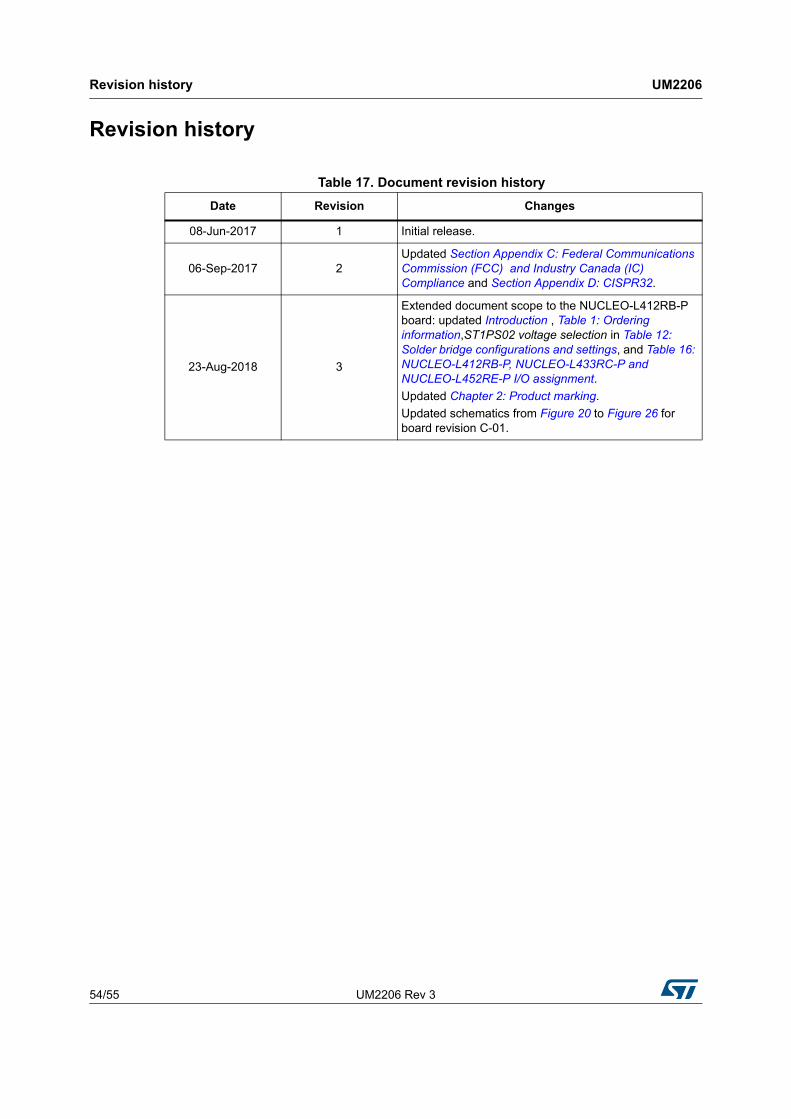
Revision history UM2206
54/55 UM2206 Rev 3
Revision history
Table 17. Document revision history
Date Revision Changes
08-Jun-2017 1 Initial release.
06-Sep-2017 2Updated Section Appendix C: Federal Communications Commission (FCC) and Industry Canada (IC) Compliance and Section Appendix D: CISPR32.
23-Aug-2018 3
Extended document scope to the NUCLEO-L412RB-P board: updated Introduction , Table 1: Ordering information,ST1PS02 voltage selection in Table 12: Solder bridge configurations and settings, and Table 16: NUCLEO-L412RB-P, NUCLEO-L433RC-P and NUCLEO-L452RE-P I/O assignment.
Updated Chapter 2: Product marking.
Updated schematics from Figure 20 to Figure 26 for board revision C-01.
UM2206 Rev 3 55/55
UM2206
55
IMPORTANT NOTICE – PLEASE READ CAREFULLY
STMicroelectronics NV and its subsidiaries (“ST”) reserve the right to make changes, corrections, enhancements, modifications, and improvements to ST products and/or to this document at any time without notice. Purchasers should obtain the latest relevant information on ST products before placing orders. ST products are sold pursuant to ST’s terms and conditions of sale in place at the time of order acknowledgement.
Purchasers are solely responsible for the choice, selection, and use of ST products and ST assumes no liability for application assistance or the design of Purchasers’ products.
No license, express or implied, to any intellectual property right is granted by ST herein.
Resale of ST products with provisions different from the information set forth herein shall void any warranty granted by ST for such product.
ST and the ST logo are trademarks of ST. All other product or service names are the property of their respective owners.
Information in this document supersedes and replaces information previously supplied in any prior versions of this document.
© 2018 STMicroelectronics – All rights reserved