Embed Size (px)
Citation preview

Stepped Supply Voltage Switching
for Energy Constrained Systems
Sudhanshu Khanna, Kyle Craig, Yousef Shakhsheer, Saad Arrabi,
John Lach, and Benton Calhoun
Charles L. Brown Department of Electrical and Computer Engineering
University of Virginia

Low Power Systems
• Contemporary Applications
– Cellphones
– Tablets
• Emerging Applications
– Wearable and Implantable Medical Systems
– Environmental Sensors
2

Low Power Systems
• Limited Battery Life
• Low Power Modes:
– Power Gating – Power Gating
– Retention Mode
– Dynamic Voltage Scaling (DVS)
• Cost associated with going into and coming out of a low power mode
3

Overview
• Introduction
• Stepped Supply Voltage Switching (SVS):
Introduction and Theoretical Analysis
• Simulation & Measurement Results• Simulation & Measurement Results
• Noise Reduction using SVS
• Conclusions
4

DVS Variants
Voltage supply of a block should track the block’s required delay
VDD
B1 B2
VDDH
B1 B2
VDDL
B3 B3
Single-VDD DVS
• VDD of entire chip is varied
• Lot of block level slack is wasted
• DC-DC converter controls VDD
• Varying the supply is slow
Multi-VDD DVS
• VDD of entire “voltage domain” is varied
• Static VDD-Block scheduling
• DC-DC converter(s) controls VDDL and VDDH
• Varying the supply is slow
5

DVS Variants: Panoptic DVS
• Dynamic VDD-block scheduling
• Number of supplies can be greater than 2
VDDHVDDL
VDDH
VDDMVDDL
B1 B2
B3
• Varying the supply to a block is fast
VDDL VDDM VDDH
VDDH
B1 Virtual Rail
VDDL VDDM VDDH
B2
6Ref: Putic “Panoptic DVS: A fine-grained dynamic voltage scaling..” ICCD 2009
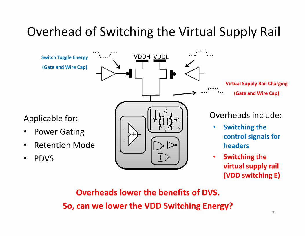
Overhead of Switching the Virtual Supply Rail
VDDHSwitch Toggle Energy
(Gate and Wire Cap)
Virtual Supply Rail Charging
(Gate and Wire Cap)
Applicable for: Overheads include:
VDDL
Applicable for:
• Power Gating
• Retention Mode
• PDVS
Overheads include:
• Switching the
control signals for
headers
• Switching the
virtual supply rail
(VDD switching E)
Overheads lower the benefits of DVS.
So, can we lower the VDD Switching Energy?7

Overview
• Introduction
• Stepped Supply Voltage Switching (SVS):
Introduction and Theoretical Analysis
• Simulation & Measurement Results• Simulation & Measurement Results
• Noise Reduction using SVS
• Conclusions
8

Stepped Supply Voltage Switching (SVS)
• We use SVS to lower the VDD switching energy during:– Power gated mode to VDDH
– VDDL to VDDH
• PDVS systems already have the extra VDDM rail– Thus, no need to add dedicated rail for implementing SVS– Thus, no need to add dedicated rail for implementing SVS
VDDHVDDL VDDM
Circuit
Block
VGM VGH
VGL
VGMVirtual VDD
VGLVDDH
VDDM
VDDL
VGH
VDDM control voltage is pulsed while going from VDDL to VDDH
9
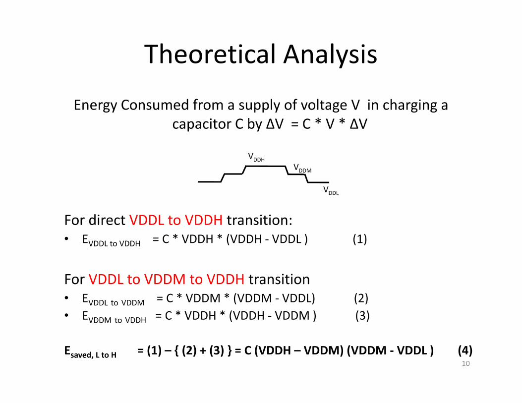
Theoretical Analysis
Energy Consumed from a supply of voltage V in charging a
capacitor C by ∆V = C * V * ∆V
VDDH
VDDM
VDDL
For direct VDDL to VDDH transition:
• EVDDL to VDDH = C * VDDH * (VDDH - VDDL ) (1)
For VDDL to VDDM to VDDH transition
• EVDDL to VDDM = C * VDDM * (VDDM - VDDL) (2)
• EVDDM to VDDH = C * VDDH * (VDDH - VDDM ) (3)
Esaved, L to H = (1) – { (2) + (3) } = C (VDDH – VDDM) (VDDM - VDDL ) (4)10

Theoretical Analysis (cont.)
Energy Consumed from a supply of voltage V in charging a
capacitor C by ∆V = C * V * ∆V
VDDH
VDDM
VDDLFor direct VDDH to VDDL transition:
E = C * VDDL * (VDDL - VDDH ) (5)
11
• EVDDH to VDDL = C * VDDL * (VDDL - VDDH ) (5)
For VDDH to VDD to VDDL transition
• EVDDH to VDDM = C * VDDM * (VDDM - VDDH) (6)
• EVDDM to VDDL = C * VDDL * (VDDL - VDDM ) (7)
Esaved, H to L = (5) – { (6) + (7) } = C (VDDH – VDDM) (VDDM - VDDL ) (8)
Esaved, total = (7) + (4) = 2* C (VDDH – VDDM) (VDDM - VDDL ) (9)

Theoretical Energy Savings
• Largest when VDDM is midway between VDDL and VDDH
• % Energy Saving
– 1 intermediate step ( i.e. VDDL to VDDM to VDDH) : 50%
– 2 intermediate steps ( i.e. VDDL to VDDM1 to VDDM2 to VDDH) : 66%– 2 intermediate steps ( i.e. VDDL to VDDM1 to VDDM2 to VDDH) : 66%
0.4 0.5 0.6 0.7 0.8 0.9 1.0 1.1
0.1
0.2
0.3
0.4
0.5
VDDM
(V)
En
ergy S
avin
gs
Worst Case
Best Case
Energy saved (normalized) vs VDDM
(VDDL = 0.3V VDDH = 1.2V)
12

Overview
• Introduction
• Stepped Supply Voltage Switching (SVS):
Introduction and Theoretical Analysis
• Simulation & Measurement Results• Simulation & Measurement Results
• Noise Reduction using SVS
• Conclusions
13

Energy savings using SVS: Simulations
• VDDH = 1.2V, VDDL is varied
• Saving is lower than ideal because of:– Energy consumed in switching intermediate supply headers (e.g. VGM)
– This overhead increases in % as VDDL increases
• 45% at 0.3V and 30% at 0.8V in the one-step multiplier case (ideal is 50%)
0.3
En
erg
y S
av
ing
s
1 Step
2 Step
3 Step0.5
0.6
En
ergy S
avin
gs
1 Step
2 Step
3 Step
0.3 0.4 0.5 0.6 0.7 0.8
−0.5
−0.3
−0.1
0.1
VDDL
(V)
En
erg
y S
av
ing
s
0.3 0.4 0.5 0.6 0.7 0.8
0.1
0.2
0.3
0.4
0.5
VDDL
(V)E
ner
gy S
avin
gs
VDDHVDDL VDDM
Circuit Block
VGM VGH
VGL
VGMVirtual VDD
VGLVDDH
VDDM
VDDL
VGH
32b Adder 32b Multiplier
Waveforms for 1-step SVS14
Ideal savings
for 1-step

Energy savings using SVS: Measurements
• VDDH= 1.2V, for 32b multiplier
• VDDL is varied, VDDM is kept midway
• Measured and simulated trends match closely
• As before, benefits fall as VDDL rises, and header toggling energy starts dominating
0.4 0.5 0.6 0.7 0.80
10
20
30
40
VDDL
(V)
VD
D S
wit
chin
g E
ner
gy (
pJ)
Simulated w/o SVS
Measured w/o SVS
Simulated w/ SVS
Measured w/ SVS
Die photo of 90nm test-chip
15

Overview
• Introduction
• Stepped Supply Voltage Switching (SVS):
Introduction and Theoretical Analysis
• Simulation & Measurement Results• Simulation & Measurement Results
• Noise Reduction using SVS
• Conclusions
16

SVS and Power Supply Noise
• Noise = Ldi/dt
• SVS reduces noise by:– Reducing the energy consumed in the transition (decrease in “di”)
• For a system using PDVS, the benefit comes with no need for additional circuitry additional circuitry
VDDHVDDL VDDM
Circuit Block
Supplyto block
Supply pin
LPKG
RPKG + RRAIL
CDECAP
VDDL VDDL to VDDM to VDDH
(With SVS)
VDDL to VDDH
(Without SVS)
0.3V 80 mV 137 mV
0.6V 55 mV 105 mV
0.9V 33 mV 58 mV
Setup:
• VDDH = 1.2V, VDDM midway between VDDL and VDDH
• 32b adder along with LPKG = 10nH, RPKG + RRAIL =20ohm
and CDECAP =10pF
SVS lowers noise by 40%
17

Conclusions
• VDD switching energy and power supply noise are critical metrics in systems using DVS and power gating
• SVS leverages existing DVS infrastructure, thus is low in overheadoverhead
• VDD switching energy is lowered by a factor of 45% for a 32b multiplier, and by 35% for a 32b adder
• Power supply noise is reduced by 40% as compared to conventional power gating or DVS
18

Thanks!
19