Embed Size (px)
Citation preview
Static Timing Overview with intro to FPGAs
Prof. MacDonald
Static Timing
In the 70’s timing was performed with Spice simulation In the 80’s timing was included in Verilog simulation to
determine if design was sufficiently fast. Two problems with either approach (Dynamic Timing):
1) Analysis was only as good as simulations – a problem was only found if exercised by the sim
2) Logic simulations were 5-10 times slower Static Timing is more comprehensive. Calculate the
delay for every possible logical path in the design. The worst case path determines the max freq.
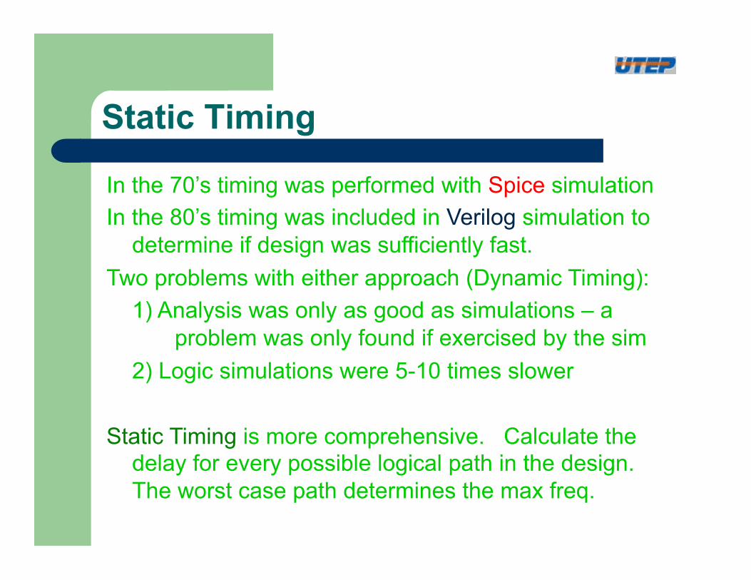
Setup Timing – flop to flop
Check that signal arrives in time for the clock
Can be solved by:
1) simply slowing down the clock,
2) reducing logic delay between flops
3) using faster flip-flops
http://www.xilinx.com/support/sw_manuals/2_1i/download/timing.pdf
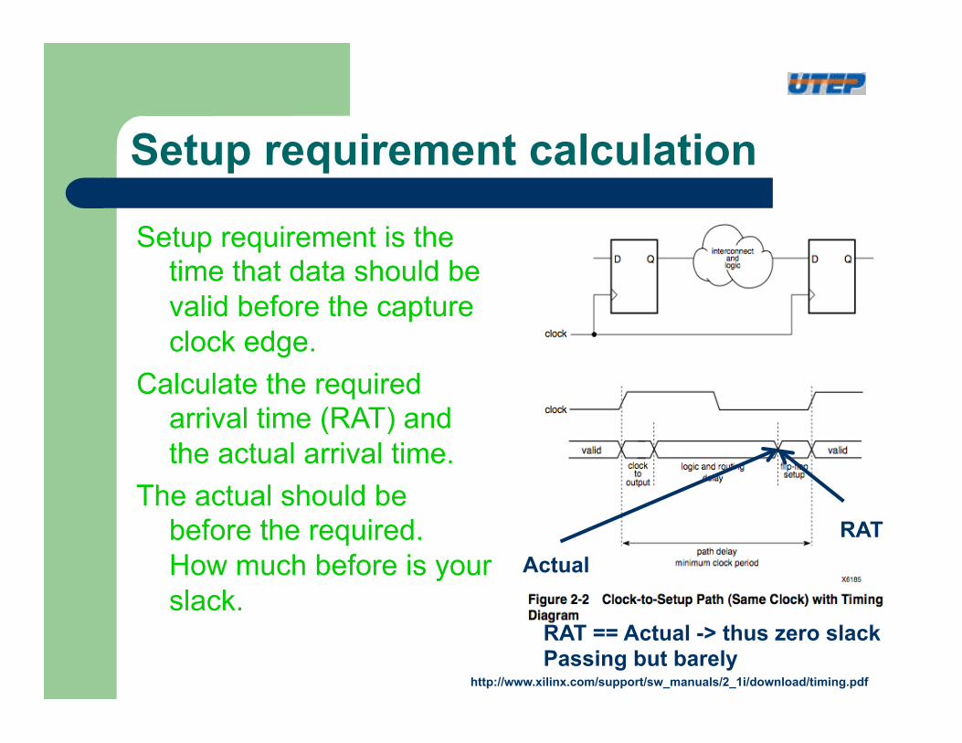
Setup requirement calculation
Setup requirement is the time that data should be valid before the capture clock edge.
Calculate the required arrival time (RAT) and the actual arrival time.
The actual should be before the required. How much before is your slack.
http://www.xilinx.com/support/sw_manuals/2_1i/download/timing.pdf
RAT Actual
RAT == Actual -> thus zero slack Passing but barely
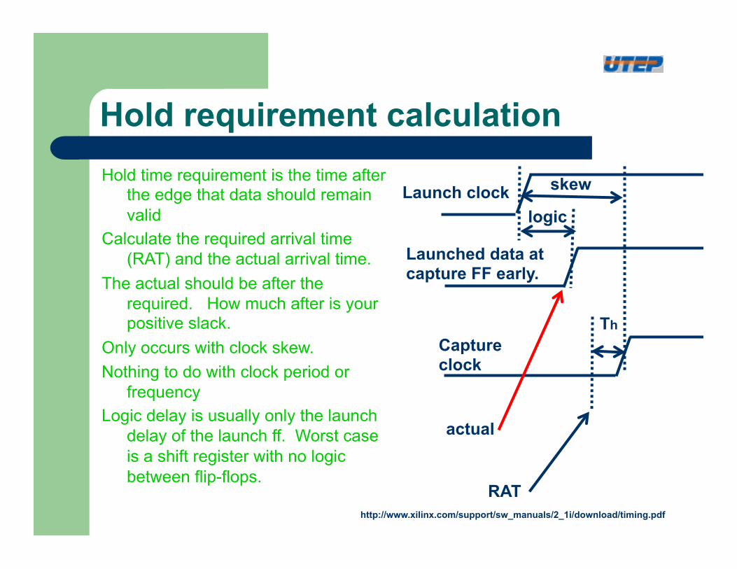
Hold requirement calculation Hold time requirement is the time after
the edge that data should remain valid
Calculate the required arrival time (RAT) and the actual arrival time.
The actual should be after the required. How much after is your positive slack.
Only occurs with clock skew. Nothing to do with clock period or
frequency Logic delay is usually only the launch
delay of the launch ff. Worst case is a shift register with no logic between flip-flops.
http://www.xilinx.com/support/sw_manuals/2_1i/download/timing.pdf
Launch clock
Capture clock
Launched data at capture FF early.
actual
RAT
Th
skew
logic
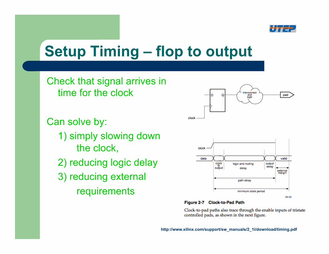
Setup Timing – flop to output
Check that signal arrives in time for the clock
Can solve by:
1) simply slowing down the clock,
2) reducing logic delay 3) reducing external requirements
http://www.xilinx.com/support/sw_manuals/2_1i/download/timing.pdf
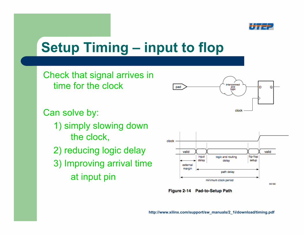
Setup Timing – input to flop
Check that signal arrives in time for the clock
Can solve by:
1) simply slowing down the clock,
2) reducing logic delay 3) Improving arrival time at input pin
http://www.xilinx.com/support/sw_manuals/2_1i/download/timing.pdf
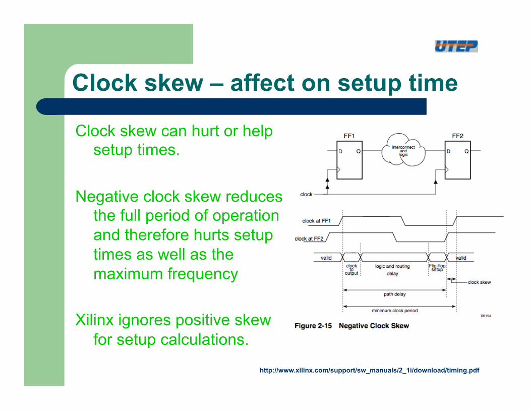
Clock skew – affect on setup time
Clock skew can hurt or help setup times.
Negative clock skew reduces
the full period of operation and therefore hurts setup times as well as the maximum frequency
Xilinx ignores positive skew
for setup calculations.
http://www.xilinx.com/support/sw_manuals/2_1i/download/timing.pdf
http://www.xilinx.com/support/sw_manuals/2_1i/download/timing.pdf
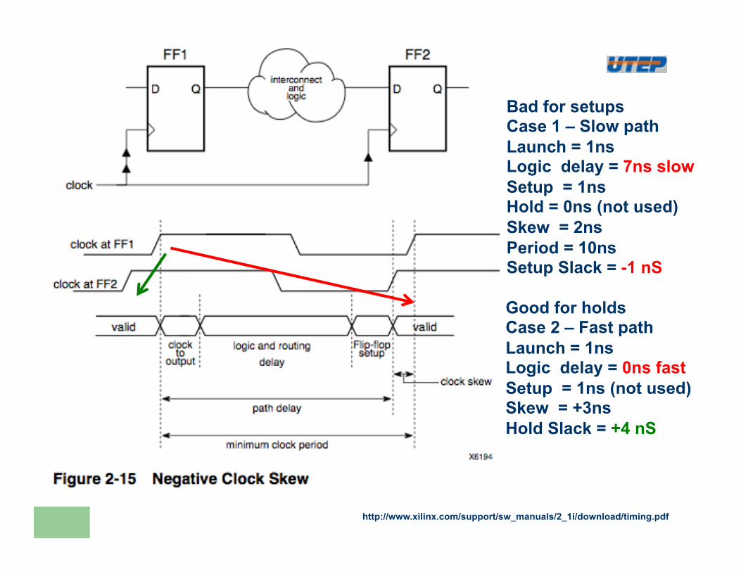
Bad for setups Case 1 – Slow path Launch = 1ns Logic delay = 7ns slow Setup = 1ns Hold = 0ns (not used) Skew = 2ns Period = 10ns Setup Slack = -1 nS
Good for holds Case 2 – Fast path Launch = 1ns Logic delay = 0ns fast Setup = 1ns (not used) Skew = +3ns Hold Slack = +4 nS
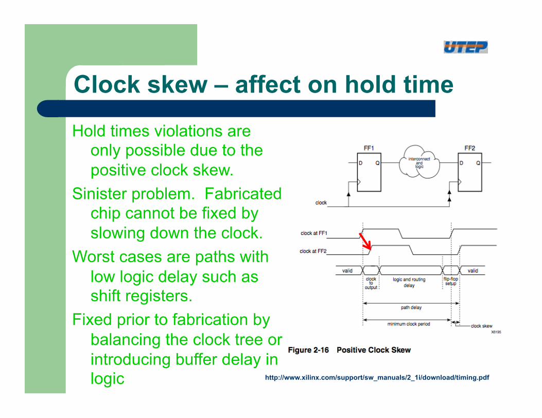
Clock skew – affect on hold time
Hold times violations are only possible due to the positive clock skew.
Sinister problem. Fabricated chip cannot be fixed by slowing down the clock.
Worst cases are paths with low logic delay such as shift registers.
Fixed prior to fabrication by balancing the clock tree or introducing buffer delay in logic
http://www.xilinx.com/support/sw_manuals/2_1i/download/timing.pdf
Clock skew – affect on hold time
http://www.xilinx.com/support/sw_manuals/2_1i/download/timing.pdf
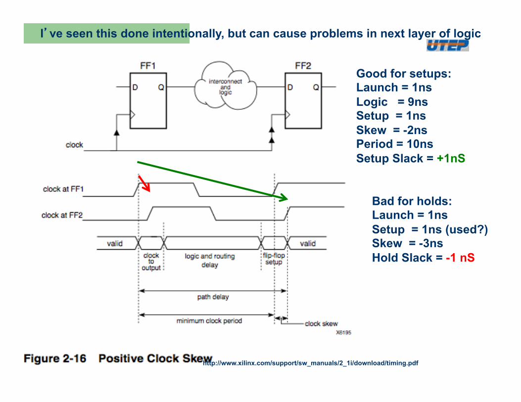
Good for setups: Launch = 1ns Logic = 9ns Setup = 1ns Skew = -2ns Period = 10ns Setup Slack = +1nS
Bad for holds: Launch = 1ns Setup = 1ns (used?) Skew = -3ns Hold Slack = -1 nS
I’ve seen this done intentionally, but can cause problems in next layer of logic
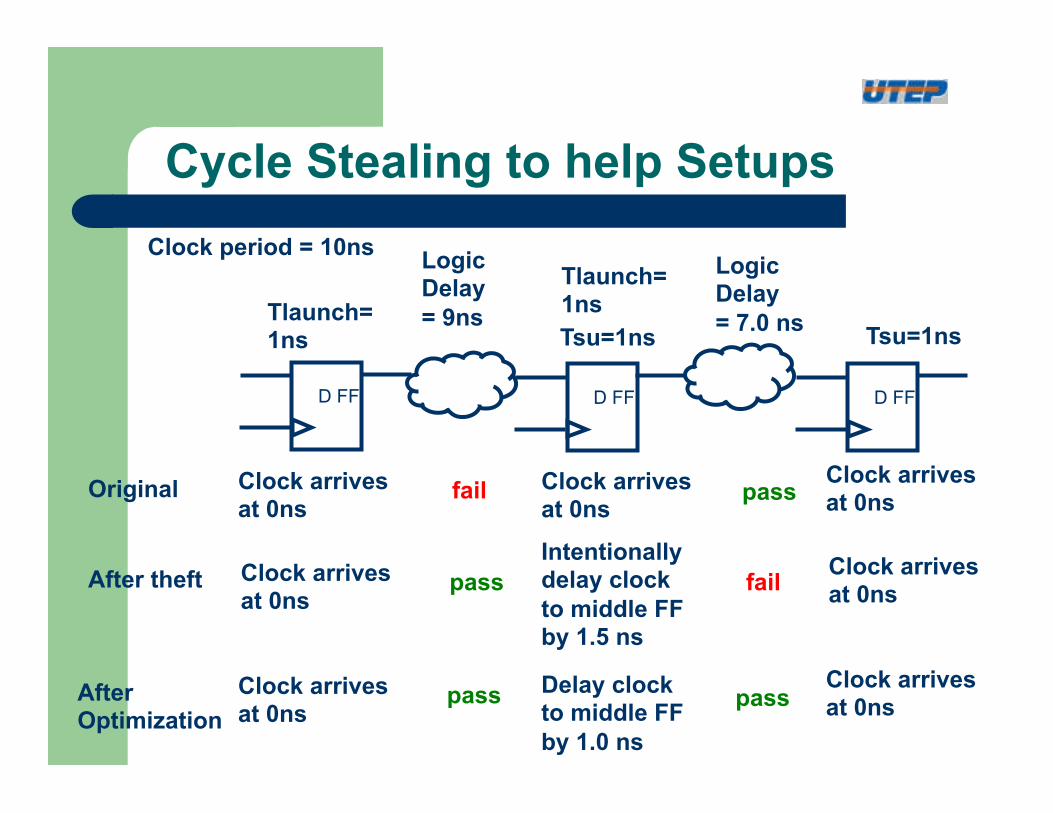
Cycle Stealing to help Setups
D FF D FF
Tsu=1ns Tlaunch= 1ns
D FF
Tsu=1ns
Tlaunch= 1ns
Clock arrives at 0ns
Clock arrives at 0ns
Clock arrives at 0ns
Logic Delay = 9ns
Logic Delay = 7.0 ns
Clock period = 10ns
Clock arrives at 0ns
Intentionallydelay clock to middle FF by 1.5 ns
Clock arrives at 0ns
fail pass
pass fail
Original
After theft
Clock arrives at 0ns
Delay clock to middle FF by 1.0 ns
Clock arrives at 0ns pass After
Optimization pass
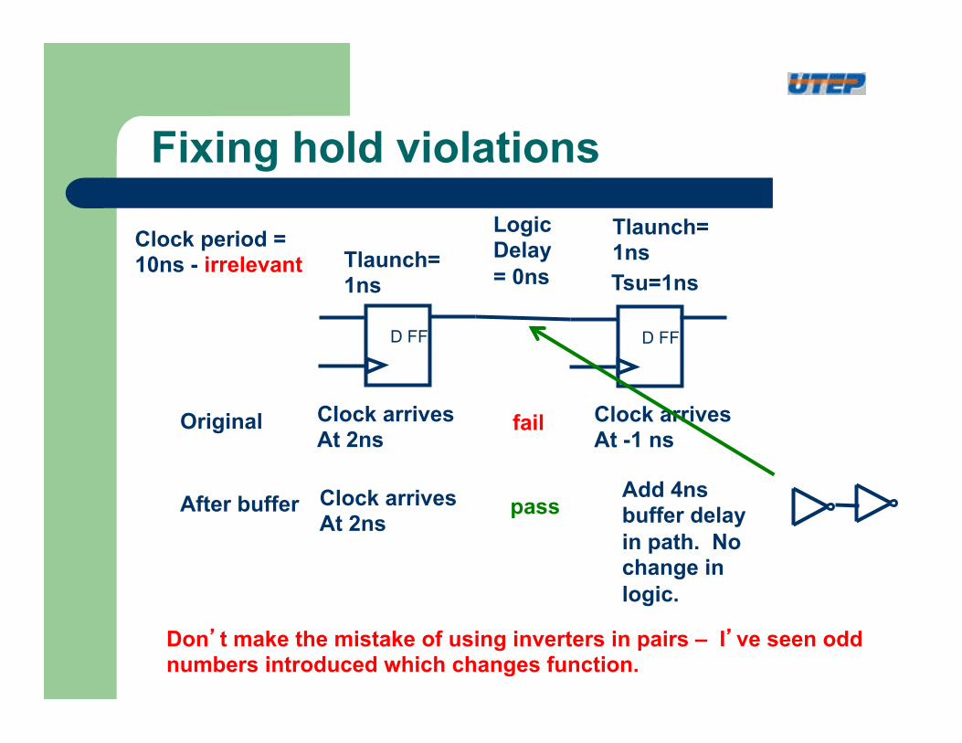
Fixing hold violations
D FF D FF
Tsu=1ns Tlaunch= 1ns
Tlaunch= 1ns
Clock arrives At 2ns
Clock arrives At -1 ns
Logic Delay = 0ns
Clock period = 10ns - irrelevant
Clock arrives At 2ns
Add 4ns buffer delay in path. No change in logic.
fail
pass
Original
After buffer
Don’t make the mistake of using inverters in pairs – I’ve seen odd numbers introduced which changes function.
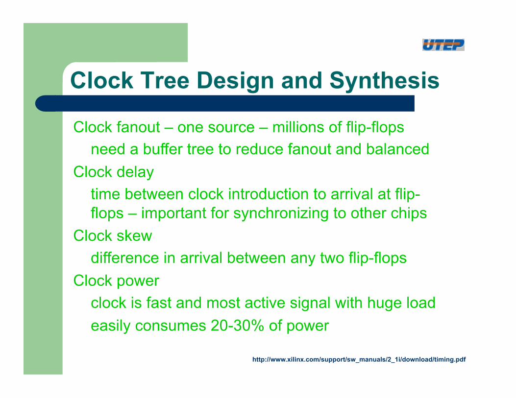
Clock Tree Design and Synthesis
http://www.xilinx.com/support/sw_manuals/2_1i/download/timing.pdf
Clock fanout – one source – millions of flip-flops need a buffer tree to reduce fanout and balanced
Clock delay time between clock introduction to arrival at flip-flops – important for synchronizing to other chips
Clock skew difference in arrival between any two flip-flops
Clock power clock is fast and most active signal with huge load easily consumes 20-30% of power
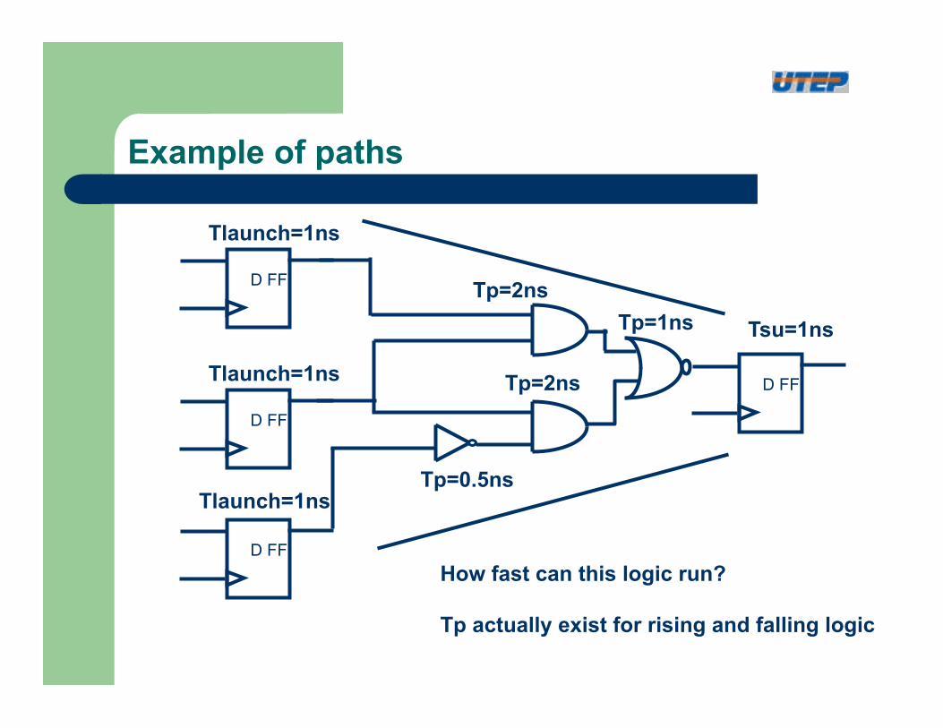
Example of paths
D FF
D FF
D FF
D FF
Tsu=1ns Tp=1ns Tp=2ns
Tp=2ns
Tlaunch=1ns
Tp=0.5ns
Tlaunch=1ns
Tlaunch=1ns
How fast can this logic run? Tp actually exist for rising and falling logic
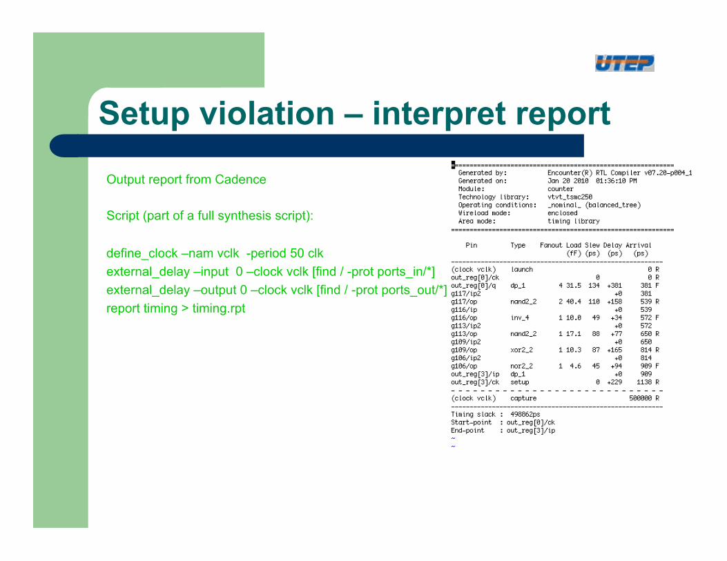
Setup violation – interpret report
Output report from Cadence Script (part of a full synthesis script): define_clock –nam vclk -period 50 clk external_delay –input 0 –clock vclk [find / -prot ports_in/*] external_delay –output 0 –clock vclk [find / -prot ports_out/*] report timing > timing.rpt
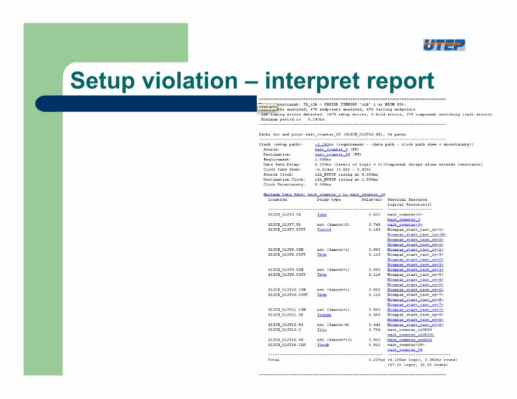
Setup violation – interpret report
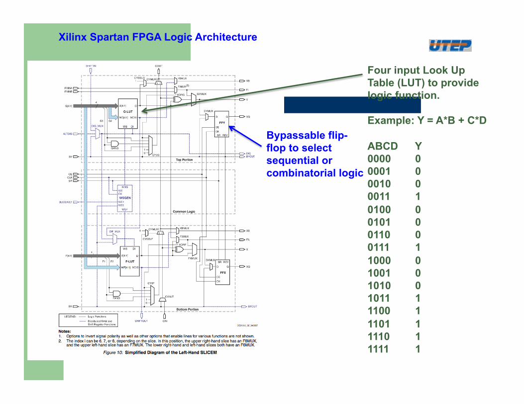
Four input Look Up Table (LUT) to provide logic function. Example: Y = A*B + C*D ABCD Y 0000 0 0001 0 0010 0 0011 1 0100 0 0101 0 0110 0 0111 1 1000 0 1001 0 1010 0 1011 1 1100 1 1101 1 1110 1 1111 1
Bypassable flip-flop to select sequential or combinatorial logic
Xilinx Spartan FPGA Logic Architecture
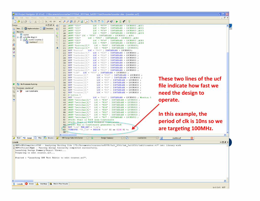
These two lines of the ucf file indicate how fast we need the design to operate. In this example, the period of clk is 10ns so we are targe=ng 100MHz.
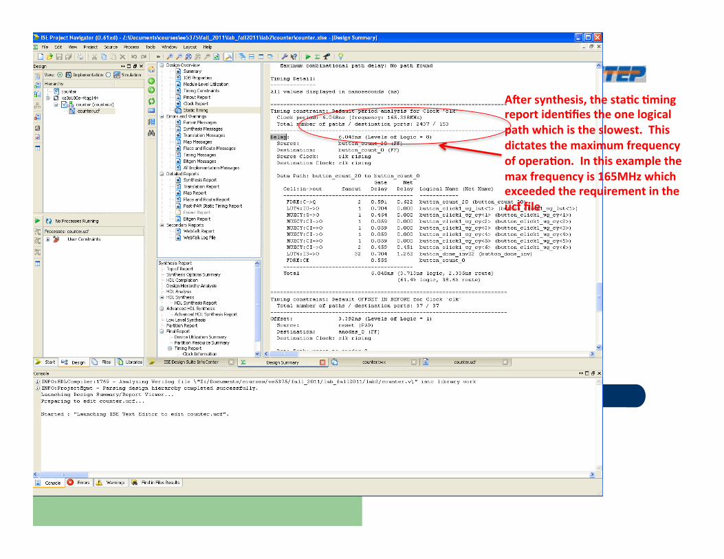
ABer synthesis, the sta=c =ming report iden=fies the one logical path which is the slowest. This dictates the maximum frequency of opera=on. In this example the max frequency is 165MHz which exceeded the requirement in the ucf file
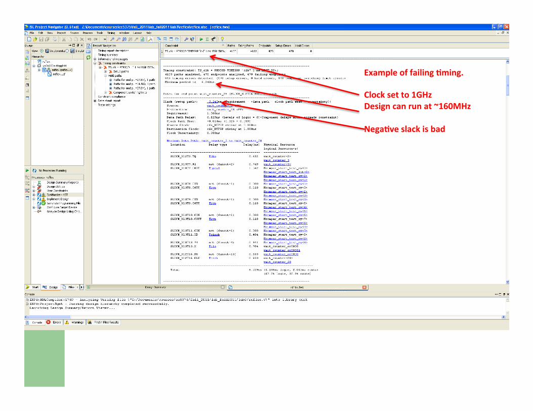
Example of failing =ming. Clock set to 1GHz Design can run at ~160MHz Nega=ve slack is bad
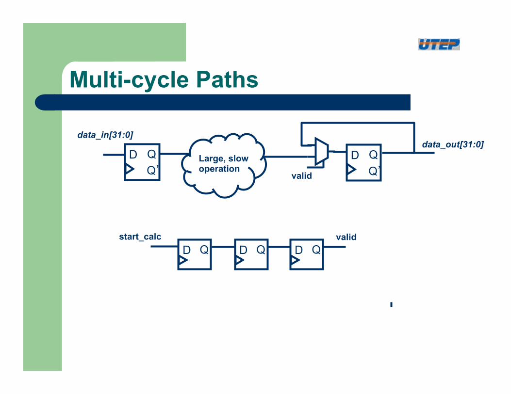
Multi-cycle Paths
D Q D Q D Q valid
D Q Q’
D Q Q’
data_in[31:0] data_out[31:0]
valid
start_calc
Large, slow operation
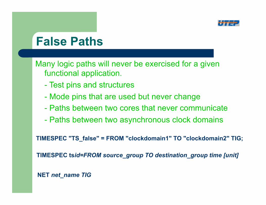
False Paths Many logic paths will never be exercised for a given
functional application. - Test pins and structures - Mode pins that are used but never change - Paths between two cores that never communicate - Paths between two asynchronous clock domains
TIMESPEC "TS_false" = FROM "clockdomain1" TO "clockdomain2" TIG;
TIMESPEC tsid=FROM source_group TO destination_group time [unit]
NET net_name TIG
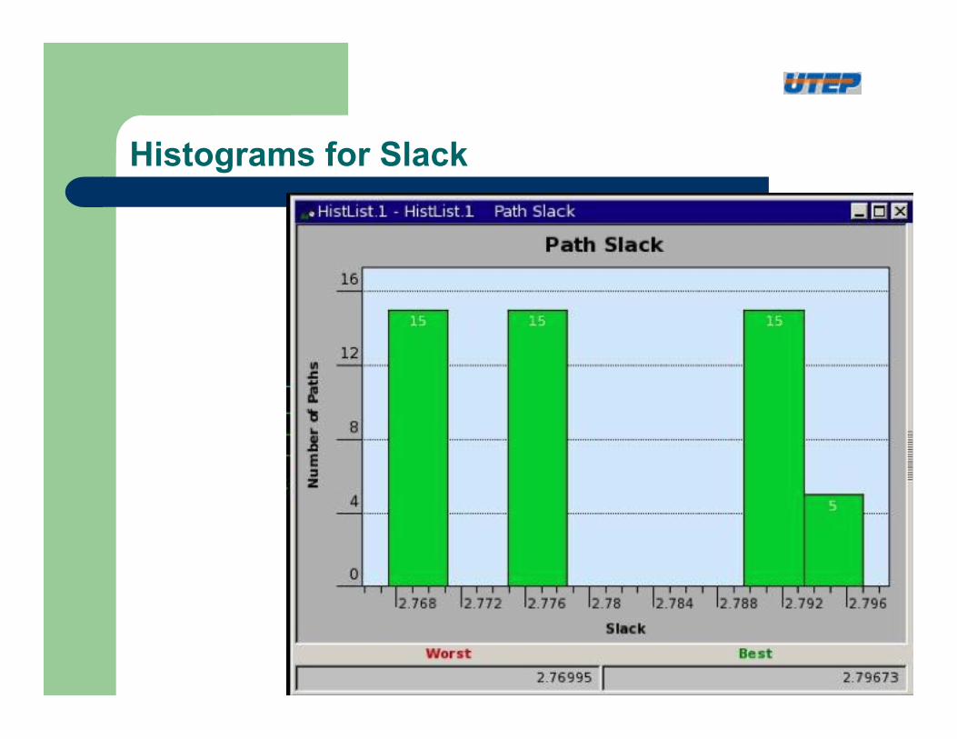
Histograms for Slack