Embed Size (px)
Citation preview
STATE SPACE MODELLING OF CURRENT-MODE CONTROL
AND ITS APPLICATION TO INPUT IMPEDANCE SHAPING OF
POWER ELECTRONIC CONSTANT-POWER LOADS
Sean C. Smithson
A thesis
in
The Department
of
Electrical and Computer Engineering
Presented in Partial Fulfillment of the Requirements
For the Degree of Master of Applied Science
Concordia University
Montreal, Quebec, Canada
September 2014
c© Sean C. Smithson, 2014

Concordia University
School of Graduate Studies
This is to certify that the thesis prepared
By: Sean C. Smithson
Entitled: State Space Modelling of Current-Mode Control and its Applica-
tion to Input Impedance Shaping of Power Electronic Constant-
Power Loads
and submitted in partial fulfillment of the requirements for the degree of
Master of Applied Science
complies with the regulations of this University and meets the accepted standards with respect to
originality and quality.
Signed by the final examining commitee:
Dr. M. Z. Kabir Chair
Dr. W. F. Xie Examiner
Dr. A. Aghdam Examiner
Dr. S. Williamson Supervisor
ApprovedChair of Department or Graduate Program Director
20
Christopher Trueman, Ph.D., Interim Dean
Faculty of Engineering and Computer Science
ABSTRACT
State Space Modelling of Current-Mode Control and its Application to Input
Impedance Shaping of Power Electronic Constant-Power Loads
Sean C. Smithson
Distributed DC power systems offer many benefits over AC line distribution systems such as
improved energy conversion efficiency and reduced mass due to high-frequency isolation. Unfortu-
nately, distributed DC systems with regulated bus voltages suffer from destabilising effects from
loading by downstream power electronic converters behaving as constant-power loads. Power elec-
tronic constant-power loads present a negative incremental input impedance to the main bus, which
may result in negative impedance instability. Avoiding the effects of negative impedance instabil-
ity is most often achieved by following impedance ratio criteria, such as the Middlebrook stability
criterion which has the drawback of imposing conservative constraints on the design of the power
system components. Such conservative criteria can also result in the over-design of converter input
filters and artificially imposing limits on the bandwidths of the load power electronic converters.
Through the use of a current-mode controlled pre-regulator, the input impedance of power elec-
tronic constant-power loads can be shaped to interact with the main bus impedance in a stable
manner while optimising converter bandwidth and line rejection. A new state space based approach
is developed to model peak and valley current-mode control. Following this new approach, models
for all basic DC-DC converter topologies are created (Buck, Boost and Flyback). This new model
allows for an accurate analysis of a pre-regulator and its straight forward design.
iii

Acknowledgements
First and foremost I offer my sincerest gratitude to my supervisor, Dr. Sheldon Williamson, who
gave me the opportunity to perform this research and for his patience while I juggled schooling and
working full-time.
Special thanks to my wonderful Vera, for putting up with all my late nights and absent time;
this work was as hard on her as it was on myself. And to Dexter, for understanding when I was not
always available to play.
To the management and my co-workers at MDA Space Systems for their understanding and
allowing me to take all the time off that I needed to; without it I would have never had the time
required.
Finally, I would like to thank my family for their unconditional and continued support. Thank
you Dad for your constant proof reading, criticism and comments, without them this thesis would
not have been what it turned out to be.
iv
Contents
Contents v
List of Figures vii
List of Acronyms vii
1 Introduction 1
1.1 General Introduction . . . . . . . . . . . . . . . . . . . . . . . . . . . . . . . . . . . . 1
1.1.1 Distributed DC Power Systems . . . . . . . . . . . . . . . . . . . . . . . . . . 1
1.1.2 Power Electronic Constant-Power Loads . . . . . . . . . . . . . . . . . . . . . 2
1.1.3 Modelling of Ideal Constant-Power Loads . . . . . . . . . . . . . . . . . . . . 3
1.1.4 Negative Impedance Instability . . . . . . . . . . . . . . . . . . . . . . . . . . 4
1.2 Scope of the Thesis . . . . . . . . . . . . . . . . . . . . . . . . . . . . . . . . . . . . . 6
1.3 Thesis Outline . . . . . . . . . . . . . . . . . . . . . . . . . . . . . . . . . . . . . . . 7
2 Negative Impedance Instability 8
2.1 Review of Current Control Techniques . . . . . . . . . . . . . . . . . . . . . . . . . . 11
2.1.1 Active Damping . . . . . . . . . . . . . . . . . . . . . . . . . . . . . . . . . . 11
2.1.2 Loop Cancellation . . . . . . . . . . . . . . . . . . . . . . . . . . . . . . . . . 11
2.1.3 Modified Pulse Adjustment . . . . . . . . . . . . . . . . . . . . . . . . . . . . 12
2.1.4 Digital Charge Control . . . . . . . . . . . . . . . . . . . . . . . . . . . . . . . 12
2.1.5 State Space Pole Placement . . . . . . . . . . . . . . . . . . . . . . . . . . . . 12
2.1.6 Sliding-Mode Control . . . . . . . . . . . . . . . . . . . . . . . . . . . . . . . 13
2.1.7 Synergetic Control . . . . . . . . . . . . . . . . . . . . . . . . . . . . . . . . . 13
2.1.8 Load Impedance Specification . . . . . . . . . . . . . . . . . . . . . . . . . . . 14
2.1.9 Discussion of Existing Solutions . . . . . . . . . . . . . . . . . . . . . . . . . . 14
2.2 Proposed Solution . . . . . . . . . . . . . . . . . . . . . . . . . . . . . . . . . . . . . 15
3 State Space Modelling of Current-Mode Control 17
3.1 Modelling Peak Current-Mode Control . . . . . . . . . . . . . . . . . . . . . . . . . . 17
3.1.1 The Third Order System in CCM . . . . . . . . . . . . . . . . . . . . . . . . 18
3.1.2 Modelling the PCM Controlled Buck Converter . . . . . . . . . . . . . . . . . 19
v
3.1.3 Modelling the PCM Controlled Boost Converter . . . . . . . . . . . . . . . . 25
3.1.4 Modelling the PCM Controlled Flyback Converter . . . . . . . . . . . . . . . 27
3.2 Experimental Verification of the PCM Models . . . . . . . . . . . . . . . . . . . . . . 30
3.2.1 Experimental Results of the Buck Converter . . . . . . . . . . . . . . . . . . 31
3.2.2 Experimental Results of the Boost Converter . . . . . . . . . . . . . . . . . . 34
3.2.3 Experimental Results of the Flyback Converter . . . . . . . . . . . . . . . . . 38
3.3 Modelling Valley Current-Mode Control . . . . . . . . . . . . . . . . . . . . . . . . . 40
3.3.1 Modelling the VCM Controlled Buck Converter . . . . . . . . . . . . . . . . . 41
3.3.2 Modelling the VCM Controlled Boost Converter . . . . . . . . . . . . . . . . 43
3.3.3 Modelling the VCM Controlled Flyback Converter . . . . . . . . . . . . . . . 44
3.4 Closing the Voltage-Loop . . . . . . . . . . . . . . . . . . . . . . . . . . . . . . . . . 44
3.4.1 PI Type-2 Compensator . . . . . . . . . . . . . . . . . . . . . . . . . . . . . . 45
3.4.2 Input Filter Modelling . . . . . . . . . . . . . . . . . . . . . . . . . . . . . . . 49
3.5 Comparison with Existing Models . . . . . . . . . . . . . . . . . . . . . . . . . . . . 52
3.6 Modelling Conclusions . . . . . . . . . . . . . . . . . . . . . . . . . . . . . . . . . . . 54
4 An Input Impedance Shaping Pre-Regulator 55
4.1 Proposed Pre-Regulator Topology . . . . . . . . . . . . . . . . . . . . . . . . . . . . 55
4.2 Designing the Pre-Regulator Stage . . . . . . . . . . . . . . . . . . . . . . . . . . . . 57
4.2.1 System Definition . . . . . . . . . . . . . . . . . . . . . . . . . . . . . . . . . 58
4.2.2 Pre-Regulator Power-Stage & Current-Loop Design . . . . . . . . . . . . . . . 59
4.2.3 Pre-Regulator Feed-Forward . . . . . . . . . . . . . . . . . . . . . . . . . . . . 63
4.2.4 Pre-Regulator Control Loop Design . . . . . . . . . . . . . . . . . . . . . . . 63
4.2.5 Pre-Regulator Input Filter Design . . . . . . . . . . . . . . . . . . . . . . . . 66
4.3 Cascaded System Modelling and Analysis . . . . . . . . . . . . . . . . . . . . . . . . 72
4.3.1 Modelling the Cascaded System . . . . . . . . . . . . . . . . . . . . . . . . . . 73
4.3.2 Analysis of the Cascaded System . . . . . . . . . . . . . . . . . . . . . . . . . 76
4.3.3 Practical Implementation of the Pre-Regulator Topology . . . . . . . . . . . . 77
4.3.4 Validation of the Cascaded System Model . . . . . . . . . . . . . . . . . . . . 80
5 Summary and Conclusions 85
5.1 Summary . . . . . . . . . . . . . . . . . . . . . . . . . . . . . . . . . . . . . . . . . . 85
5.2 Conclusions . . . . . . . . . . . . . . . . . . . . . . . . . . . . . . . . . . . . . . . . . 86
5.3 Suggestions for Future Work . . . . . . . . . . . . . . . . . . . . . . . . . . . . . . . 86
Bibliography 86
vi

List of Figures
1.1 Example of a distributed DC power system . . . . . . . . . . . . . . . . . . . . . . . 1
1.2 Resistive load I-V characteristics . . . . . . . . . . . . . . . . . . . . . . . . . . . . . 3
1.3 CPL I-V characteristics . . . . . . . . . . . . . . . . . . . . . . . . . . . . . . . . . . 3
1.4 Simplified CPL equivalent circuit . . . . . . . . . . . . . . . . . . . . . . . . . . . . . 4
1.5 I-V characteristics of a CPL driven by a non-zero source impedance . . . . . . . . . 5
1.6 Schematic of a simple Buck converter . . . . . . . . . . . . . . . . . . . . . . . . . . . 5
2.1 Root locus plots of positive and negative resistive loads . . . . . . . . . . . . . . . . 8
2.2 Output impedance Bode plots of a duty cycle ratio programmed Buck converter plot-
ted with increasing negative feedback . . . . . . . . . . . . . . . . . . . . . . . . . . . 9
2.3 Converter output impedance with capacitor ESL effects . . . . . . . . . . . . . . . . 10
2.4 Block diagram of initial pre-regulator topology . . . . . . . . . . . . . . . . . . . . . 15
3.1 Peak current-mode control waveforms . . . . . . . . . . . . . . . . . . . . . . . . . . 18
3.2 Schematic of example Buck converter . . . . . . . . . . . . . . . . . . . . . . . . . . . 19
3.3 Change in the duty cycle ratio (Δd), over a single switching period, due to small-signal
variations in inductor current (iL) . . . . . . . . . . . . . . . . . . . . . . . . . . . . 21
3.4 Change in the duty cycle ratio (Δd), over a single switching period, due to small-signal
variations in control signal (ictl) . . . . . . . . . . . . . . . . . . . . . . . . . . . . . . 22
3.5 Change in the duty cycle ratio (Δd), over a single switching period, due to small-signal
variations in said duty cycle (d) . . . . . . . . . . . . . . . . . . . . . . . . . . . . . . 22
3.6 Equivalent change in control signal due to compensation ramp (Ma) . . . . . . . . . 23
3.7 Equivalent change in control signal due to propagation delay effects . . . . . . . . . . 23
3.8 Schematic of example Boost converter . . . . . . . . . . . . . . . . . . . . . . . . . . 26
3.9 Schematic of example Flyback converter . . . . . . . . . . . . . . . . . . . . . . . . . 28
3.10 Photograph of experimental test Boost and Flyback converters . . . . . . . . . . . . 30
3.11 Photograph of experimental test Buck converter . . . . . . . . . . . . . . . . . . . . 31
3.12 PCM controlled Buck converter loop response Bode plots (solid line is Ma = 0.2M2,
dashed line is Ma = 5M2) . . . . . . . . . . . . . . . . . . . . . . . . . . . . . . . . . 32
3.13 PCM controlled Buck converter conducted susceptibility Bode plots (solid line is
Ma = 0.1M2, dashed line is Ma = 37.5M2) . . . . . . . . . . . . . . . . . . . . . . . . 33
3.14 PCM controlled Buck converter input impedance Bode plots (solid line is Ma =
0.2M2, dashed line is Ma = 37.5M2) . . . . . . . . . . . . . . . . . . . . . . . . . . . 33
vii
3.15 PCM controlled Buck converter output impedance Bode plots (Ma = 0.1M2) . . . . 34
3.16 PCM controlled Boost converter loop response Bode plots (solid line is Ma = 0.1M2,
dashed line is Ma = 2M2) . . . . . . . . . . . . . . . . . . . . . . . . . . . . . . . . . 35
3.17 PCM controlled Boost converter conducted susceptibility Bode plots (solid line is
Ma = 0.1M2, dashed line is Ma = 5M2) . . . . . . . . . . . . . . . . . . . . . . . . . 36
3.18 PCM controlled Boost converter input impedance Bode plots (solid line is Ma =
0.1M2, dashed line is Ma = 5M2) . . . . . . . . . . . . . . . . . . . . . . . . . . . . . 37
3.19 PCM controlled Boost converter output impedance Bode plots (Ma = 0.2M2) . . . . 37
3.20 PCM controlled Flyback converter loop response Bode plots (solid line isMa = 0.1M2,
dashed line is Ma = M2) . . . . . . . . . . . . . . . . . . . . . . . . . . . . . . . . . . 38
3.21 PCM controlled Flyback converter conducted susceptibility Bode plots (solid line is
Ma = 0.2M2, dashed line is Ma = 5M2) . . . . . . . . . . . . . . . . . . . . . . . . . 39
3.22 PCM controlled Flyback converter input impedance Bode plots (solid line is Ma =
0.2M2, dashed line is Ma = 37.5M2) . . . . . . . . . . . . . . . . . . . . . . . . . . . 40
3.23 PCM controlled Flyback converter output impedance Bode plots (Ma = 0.2M2) . . . 41
3.24 Valley current-mode control waveforms in CCM . . . . . . . . . . . . . . . . . . . . . 42
3.25 Sub-harmonic oscillation in VCM . . . . . . . . . . . . . . . . . . . . . . . . . . . . . 42
3.26 VCM controlled Buck converter loop response Bode plots . . . . . . . . . . . . . . . 43
3.27 VCM controlled Boost converter conducted susceptibility Bode plots . . . . . . . . . 44
3.28 PI Type-2 compensator equivalent schematic . . . . . . . . . . . . . . . . . . . . . . 45
3.29 Buck Converter with PI Type-2 compensator loop response Bode plot . . . . . . . . 47
3.30 Buck Converter with PI Type-2 compensator closed-loop conducted susceptibility
Bode plot . . . . . . . . . . . . . . . . . . . . . . . . . . . . . . . . . . . . . . . . . . 47
3.31 Buck Converter with PI Type-2 compensator closed-loop input impedance Bode plot 48
3.32 Buck Converter with PI Type-2 compensator closed-loop output impedance Bode plot 48
3.33 Schematic of a typical fourth-order DC-DC converter input filter . . . . . . . . . . . 49
3.34 Input filter output impedance & converter input impedance . . . . . . . . . . . . . . 52
3.35 Input filter effects on converter input impedance . . . . . . . . . . . . . . . . . . . . 53
3.36 Variations in conducted susceptibility due to increasing controller turn-off delays . . 54
4.1 Block diagram of pre-regulator topology with voltage feed-forward . . . . . . . . . . 56
4.2 Block diagram of pre-regulator operating at low frequencies . . . . . . . . . . . . . . 56
4.3 Block diagram of pre-regulator operating at frequencies above error-amplifier bandwidth 57
4.4 Block diagram of cascaded pre-regulator and load converter . . . . . . . . . . . . . . 58
4.5 Example load converter loop response Bode plot . . . . . . . . . . . . . . . . . . . . 59
4.6 Example load converter conducted susceptibility Bode plot . . . . . . . . . . . . . . 60
4.7 Example load converter input impedance Bode plot . . . . . . . . . . . . . . . . . . . 60
4.8 Example pre-regulator initial loop response root locus plot . . . . . . . . . . . . . . . 61
4.9 Example pre-regulator loop response root locus plot with desired feedback . . . . . . 62
4.10 Example pre-regulator Zin pole-zero map without input voltage feed-forward . . . . 63
4.11 Example pre-regulator Zin pole-zero map with input voltage feed-forward . . . . . . 64
viii

4.12 Example pre-regulator Zin Bode plots (with and without feed-forward) . . . . . . . . 64
4.13 Example pre-regulator current-loop with added integrator loop response Bode plot . 65
4.14 Example pre-regulator loop response Bode plot . . . . . . . . . . . . . . . . . . . . . 66
4.15 Example pre-regulator closed-loop input impedance Bode plot . . . . . . . . . . . . . 67
4.16 Example pre-regulator closed-loop conducted susceptibility Bode plot . . . . . . . . 67
4.17 Example pre-regulator closed-loop output impedance Bode plot . . . . . . . . . . . . 68
4.18 Example pre-regulator input filter ripple current rejection Bode plot . . . . . . . . . 68
4.19 Example pre-regulator input impedance and filter output impedance Bode plot . . . 69
4.20 Final pre-regulator input impedance Bode plot . . . . . . . . . . . . . . . . . . . . . 71
4.21 Final pre-regulator conducted susceptibility Bode plot . . . . . . . . . . . . . . . . . 72
4.22 Cascaded pre-regulator and load converter simplified schematic . . . . . . . . . . . . 73
4.23 Bode plot of pre-regulator loop response with closed-loop load converter . . . . . . . 76
4.24 Bode plot of load converter loop response with closed pre-regulator loop . . . . . . . 77
4.25 Bode plot of cascaded system overall input to output conducted susceptibility . . . . 78
4.26 Bode plot of cascaded system overall input impedance . . . . . . . . . . . . . . . . . 78
4.27 Time domain waveform of vCi2 filter capacitor voltage . . . . . . . . . . . . . . . . . 79
4.28 Time domain modelled waveforms of Vlink due to output 1A step load at 10Hz . . . 81
4.29 Time domain measured waveforms of Vlink due to output 1A step load at 10Hz . . . 81
4.30 Time domain modelled waveforms of Vlink due to 1Vpk−pk input bus ripple at 500Hz 82
4.31 Time domain measured waveforms of Vlink due to 1Vpk−pk input bus ripple at 500Hz 82
4.32 Time domain modelled waveforms of Iin due to 1Vpk−pk input bus ripple at 500Hz . 83
4.33 Time domain measured waveforms of Iin due to 1Vpk−pk input bus ripple at 500Hz . 83
ix

List of Acronyms
CCM Continuous Conduction Mode
CPL Constant-Power Load
DCM Discontinuous Conduction Mode
ESAC Energy Source Analysis Consortium
ESL Equivalent Series Inductance
ESR Equivalent Series Resistance
FRA Frequency Response Analyser
IC Integrated Circuit
I-V Current-Voltage
MPP Molypermalloy Powder
MPPT Maximum Power Point Tracking
PCB Printed Circuit Board
PCM Peak Current-Mode
PFC Power Factor Correction
PI Proportional-Integral
POL Point-of-Load
PWM Pulse-Width Modulation
SEPIC Single-Ended Primary-Inductor Converter
SISO Single-Input Single-Output
SMC Sliding-Mode Control
SSA State Space Averaged
VCM Valley Current-Mode
x
Chapter 1
Introduction
1.1 General Introduction
1.1.1 Distributed DC Power Systems
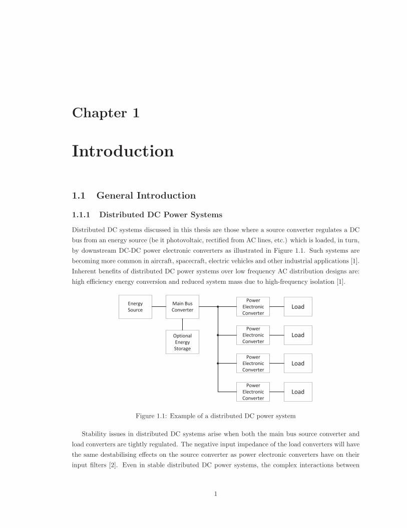
Distributed DC systems discussed in this thesis are those where a source converter regulates a DC
bus from an energy source (be it photovoltaic, rectified from AC lines, etc.) which is loaded, in turn,
by downstream DC-DC power electronic converters as illustrated in Figure 1.1. Such systems are
becoming more common in aircraft, spacecraft, electric vehicles and other industrial applications [1].
Inherent benefits of distributed DC power systems over low frequency AC distribution designs are:
high efficiency energy conversion and reduced system mass due to high-frequency isolation [1].
Figure 1.1: Example of a distributed DC power system
Stability issues in distributed DC systems arise when both the main bus source converter and
load converters are tightly regulated. The negative input impedance of the load converters will have
the same destabilising effects on the source converter as power electronic converters have on their
input filters [2]. Even in stable distributed DC power systems, the complex interactions between
1
the source converter and the multiple load converters can result in unforeseen degradation of system
performance [3].
The most often used stability criterion, enforced to ensure distributed DC power system stability,
is the Middlebrook stability criterion. This criterion is often used to guarantee the stability of input
filter and power converter combinations [4]. The Middlebrook stability criterion states that the
output impedance of the input filter (Zout) must remain well below the input impedance of the
power converter power-stage (Zin) [4]. Ensuring that Zout � Zin is a sufficient, but not necessary,
requirement to ensure that the parallel combination of Zout and Zin is positive, which in turn
guarantees stable operation.
When the Middlebrook stability criterion is applied to distributed DC power systems, the crite-
rion requires that the main bus source converter output impedance remain well below the parallel
combination of all load converter input impedances. If the Middlebrook stability criterion is met, it
is guaranteed that the converter loop response is virtually unchanged. However, this criterion does
not define at what point instability occurs when the criterion is broken. The Middlebrook stability
criterion, while simple and effective, is inherently conservative.
Other attempts to develop less conservative and more accurate stability criteria are: Gain and
Phase Margin Criterion [5], the Opposing Argument Criterion [6], the Energy Source Analysis Con-
sortium (ESAC) Criterion [7], the Root Exponential Stability Criterion [8] and the Three-Step
Impedance Criterion [9]. All of these stability criteria are, however, also sufficient but not necessary
criteria, imposing limits on the source output and load input impedances [3].
1.1.2 Power Electronic Constant-Power Loads
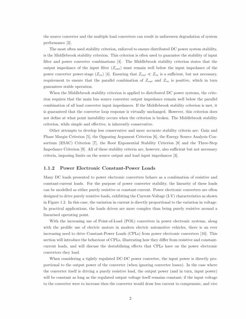
Many DC loads presented to power electronic converters behave as a combination of resistive and
constant-current loads. For the purpose of power converter stability, the linearity of these loads
can be modelled as either purely resistive or constant-current. Power electronic converters are often
designed to drive purely resistive loads, exhibiting the Current-Voltage (I-V) characteristics as shown
in Figure 1.2. In this case, the variation in current is directly proportional to the variation in voltage.
In practical applications, the loads driven are more complex than being purely resistive around a
linearised operating point.
With the increasing use of Point-of-Load (POL) converters in power electronic systems, along
with the prolific use of electric motors in modern electric automotive vehicles, there is an ever
increasing need to drive Constant-Power Loads (CPLs) from power electronic converters [10]. This
section will introduce the behaviour of CPLs, illustrating how they differ from resistive and constant-
current loads, and will discuss the destabilising effects that CPLs have on the power electronic
converters they load.
When considering a tightly regulated DC-DC power converter, the input power is directly pro-
portional to the output power of the converter (when ignoring converter losses). In the case where
the converter itself is driving a purely resistive load, the output power (and in turn, input power)
will be constant as long as the regulated output voltage itself remains constant; if the input voltage
to the converter were to increase then the converter would draw less current to compensate, and vice
2
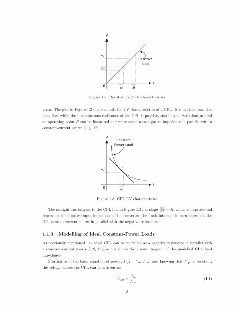
Figure 1.2: Resistive load I-V characteristics
versa. The plot in Figure 1.3 below details the I-V characteristics of a CPL. It is evident from this
plot, that while the instantaneous resistance of the CPL is positive, small signal variations around
an operating point P can be linearised and represented as a negative impedance in parallel with a
constant-current source [11], [12].
Figure 1.3: CPL I-V characteristics
The straight line tangent to the CPL line in Figure 1.3 has slope ΔVΔI = R, which is negative and
represents the negative input impedance of the converter; the I-axis intercept in turn represents the
DC constant-current source in parallel with the negative resistance.
1.1.3 Modelling of Ideal Constant-Power Loads
As previously mentioned. an ideal CPL can be modelled as a negative resistance in parallel with
a constant-current source [12], Figure 1.4 shows the circuit diagram of the modelled CPL load
impedance.
Starting from the basic equation of power, Pcpl = VoutIout, and knowing that Pcpl is constant,
the voltage across the CPL can be written as:
Vout =Pcpl
Iout(1.1)
3
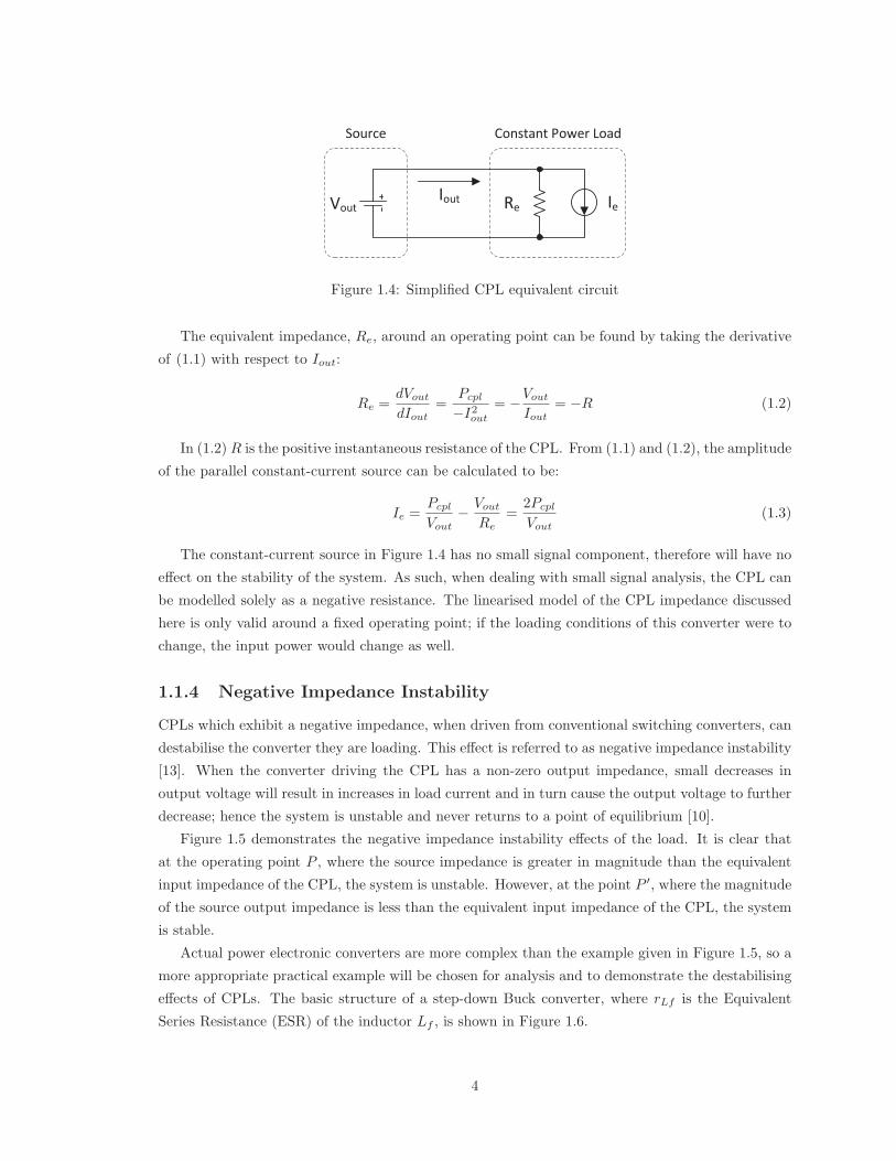
Figure 1.4: Simplified CPL equivalent circuit
The equivalent impedance, Re, around an operating point can be found by taking the derivative
of (1.1) with respect to Iout:
Re =dVout
dIout=
Pcpl
−I2out= −Vout
Iout= −R (1.2)
In (1.2) R is the positive instantaneous resistance of the CPL. From (1.1) and (1.2), the amplitude
of the parallel constant-current source can be calculated to be:
Ie =Pcpl
Vout− Vout
Re=
2Pcpl
Vout(1.3)
The constant-current source in Figure 1.4 has no small signal component, therefore will have no
effect on the stability of the system. As such, when dealing with small signal analysis, the CPL can
be modelled solely as a negative resistance. The linearised model of the CPL impedance discussed
here is only valid around a fixed operating point; if the loading conditions of this converter were to
change, the input power would change as well.
1.1.4 Negative Impedance Instability
CPLs which exhibit a negative impedance, when driven from conventional switching converters, can
destabilise the converter they are loading. This effect is referred to as negative impedance instability
[13]. When the converter driving the CPL has a non-zero output impedance, small decreases in
output voltage will result in increases in load current and in turn cause the output voltage to further
decrease; hence the system is unstable and never returns to a point of equilibrium [10].
Figure 1.5 demonstrates the negative impedance instability effects of the load. It is clear that
at the operating point P , where the source impedance is greater in magnitude than the equivalent
input impedance of the CPL, the system is unstable. However, at the point P ′, where the magnitude
of the source output impedance is less than the equivalent input impedance of the CPL, the system
is stable.
Actual power electronic converters are more complex than the example given in Figure 1.5, so a
more appropriate practical example will be chosen for analysis and to demonstrate the destabilising
effects of CPLs. The basic structure of a step-down Buck converter, where rLf is the Equivalent
Series Resistance (ESR) of the inductor Lf , is shown in Figure 1.6.
4
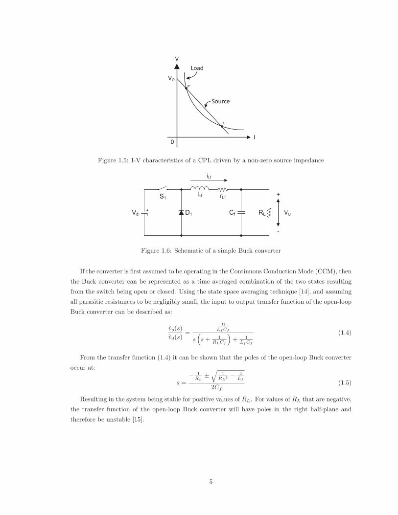
Figure 1.5: I-V characteristics of a CPL driven by a non-zero source impedance
S1
Vd D1 Cf
Lf
RL
rLf
Figure 1.6: Schematic of a simple Buck converter
If the converter is first assumed to be operating in the Continuous Conduction Mode (CCM), then
the Buck converter can be represented as a time averaged combination of the two states resulting
from the switch being open or closed. Using the state space averaging technique [14], and assuming
all parasitic resistances to be negligibly small, the input to output transfer function of the open-loop
Buck converter can be described as:
vo(s)
vd(s)=
DLfCf
s(s+ 1
RLCf
)+ 1
LfCf
(1.4)
From the transfer function (1.4) it can be shown that the poles of the open-loop Buck converter
occur at:
s =− 1
RL±√
1RL
2 − 4Lf
2Cf(1.5)
Resulting in the system being stable for positive values of RL. For values of RL that are negative,
the transfer function of the open-loop Buck converter will have poles in the right half-plane and
therefore be unstable [15].
5

Considering the case where rLf is not assumed to be negligibly small, the open-loop Buck con-
verter transfer function can be written as:
vo(s)
vd(s)=
DLfCf
s2 +(
rLf
Lf+ 1
RLCf
)s+
(rLf
RLLfCf+ 1
LfCf
) (1.6)
with the poles of the transfer function now occurring at:
s =− rLfCf
Lf− 1
RL±√(
rLfCf
Lf+ 1
RL
)2− 4
(rLf
RLLf+ 1
Lf
)2Cf
(1.7)
From (1.7), it can be seen that the converter is only unstable when |RL| < Lf
rLfCfsince Lf � RL
in a properly designed power converter [16]. This relationship implies that a converter driving a
CPL can be stabilised through the use of large output filter capacitances (Cf ), small output filter
inductance (Lf ), or through damping the output filter with a large output filter inductor ESR (rLf ).
1.2 Scope of the Thesis
This thesis addresses stabilising distributed DC power systems loaded by power electronic CPLs.
The goal is to present a topology and control strategy of an Input Impedance Shaping Power
Electronic Pre-Regulator to present a positive input impedance to the source DC bus. However,
in order to accurately model the cascaded converter topology, a new small-signal State Space
Averaged Model, of Current-Mode Control, will be derived. The main objectives of this
thesis are:
i Derive a new state space average model of current-mode controlled converters operating in
CCM.
ii Validate the accuracy of the derived models with experimental results obtained from prototype
converters.
iii Develop a new pre-regulator control strategy to drive CPLs while presenting a positive input
impedance above a desired low frequency.
iv Apply the newly developed models to develop a pre-regulator cascaded topology and perform
a detailed system analysis.
6
1.3 Thesis Outline
The contents of this thesis are organised as follows. Chapter 2 introduces the instability issues
present in distributed DC power systems where power electronic converters are loaded by CPLs
with negative input impedances. Traditional stability criteria are presented and discussed. Possible
control strategies present in the current literature are also discussed and a new input impedance
shaping pre-regulator concept is introduced.
Chapter 3 presents the newly developed modelling approach for constant-frequency current-
mode control. The model is developed for all basic converter topologies: Buck, Boost and the more
practical Flyback converter (in place of the often analysed Buck-Boost topology), all operating in
CCM. This new model is then expanded to describe these three basic converter topologies operating
in CCM with the added complexity of Valley Current-Mode (VCM) control. These modelled systems
are used to design and analyse the input impedance shaping pre-regulator developed in Chapter 4.
Chapter 4 presents the final topology and control scheme of the input impedance shaping pre-
regulator presenting a positive AC input impedance to the main DC bus when loaded by a CPL.
The model developed in Chapter 3 is used to analyse the overall system stability when the pre-
regulator is loaded by a DC-DC converter. Finally, a detailed analysis provides design guidelines
for implementing the proposed pre-regulator topology and the model predictions are compared with
experimental results.
Chapter 5 summarizes the work performed and the results obtained in this thesis, including
suggestions for future work.
7
Chapter 2
Negative Impedance Instability
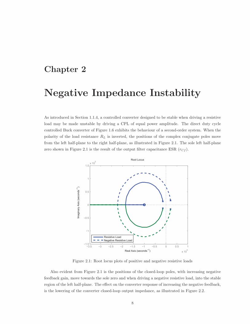
As introduced in Section 1.1.4, a controlled converter designed to be stable when driving a resistive
load may be made unstable by driving a CPL of equal power amplitude. The direct duty cycle
controlled Buck converter of Figure 1.6 exhibits the behaviour of a second-order system. When the
polarity of the load resistance RL is inverted, the positions of the complex conjugate poles move
from the left half-plane to the right half-plane, as illustrated in Figure 2.1. The sole left half-plane
zero shown in Figure 2.1 is the result of the output filter capacitance ESR (rCf ).
−3.5 −3 −2.5 −2 −1.5 −1 −0.5 0 0.5 1
x 105
−1.5
−1
−0.5
0
0.5
1
1.5x 10
5Root Locus
Real Axis (seconds−1)
Imag
inar
y A
xis
(sec
onds
−1)
Resistive LoadNegative Resistive Load
Figure 2.1: Root locus plots of positive and negative resistive loads
Also evident from Figure 2.1 is the positions of the closed-loop poles, with increasing negative
feedback gain, move towards the sole zero and when driving a negative resistive load, into the stable
region of the left half-plane. The effect on the converter response of increasing the negative feedback,
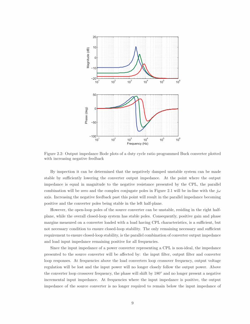
is the lowering of the converter closed-loop output impedance, as illustrated in Figure 2.2.
8
101 102 103 104 105 106−20
−10
0
10
20
Mag
nitu
de (d
B)
101 102 103 104 105 106−100
−50
0
50
Pha
se (d
eg)
Frequency (Hz)
Figure 2.2: Output impedance Bode plots of a duty cycle ratio programmed Buck converter plottedwith increasing negative feedback
By inspection it can be determined that the negatively damped unstable system can be made
stable by sufficiently lowering the converter output impedance. At the point where the output
impedance is equal in magnitude to the negative resistance presented by the CPL, the parallel
combination will be zero and the complex conjugate poles in Figure 2.1 will be in-line with the jω
axis. Increasing the negative feedback past this point will result in the parallel impedance becoming
positive and the converter poles being stable in the left half-plane.
However, the open-loop poles of the source converter can be unstable, residing in the right half-
plane, while the overall closed-loop system has stable poles. Consequently, positive gain and phase
margins measured on a converter loaded with a load having CPL characteristics, is a sufficient, but
not necessary condition to ensure closed-loop stability. The only remaining necessary and sufficient
requirement to ensure closed-loop stability, is the parallel combination of converter output impedance
and load input impedance remaining positive for all frequencies.
Since the input impedance of a power converter representing a CPL is non-ideal, the impedance
presented to the source converter will be affected by: the input filter, output filter and converter
loop responses. At frequencies above the load converters loop crossover frequency, output voltage
regulation will be lost and the input power will no longer closely follow the output power. Above
the converter loop crossover frequency, the phase will shift by 180◦ and no longer present a negative
incremental input impedance. At frequencies where the input impedance is positive, the output
impedance of the source converter is no longer required to remain below the input impedance of
9
the load, to ensure stability. Likewise, in the case where under-damped input filtering is used, the
load input impedance will have resonant valleys which will significantly lower the input impedance
at certain frequencies; to ensure stability, the source output impedance will have to remain lower
than any resonant dips.
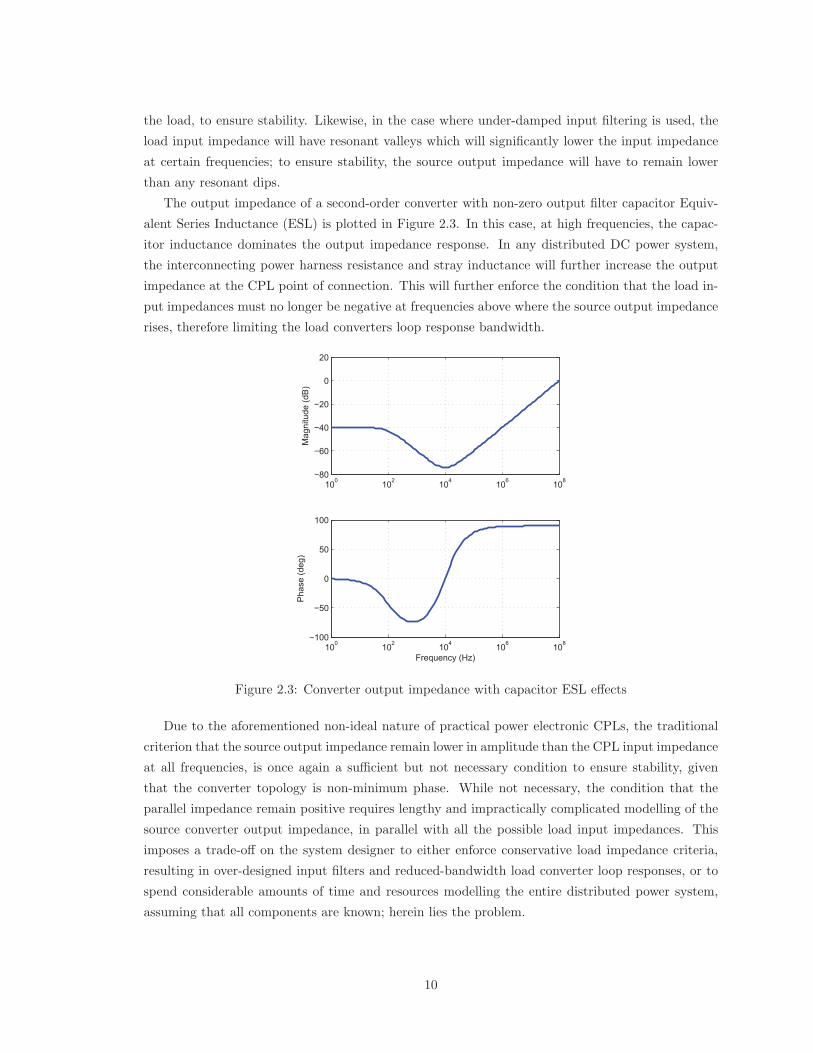
The output impedance of a second-order converter with non-zero output filter capacitor Equiv-
alent Series Inductance (ESL) is plotted in Figure 2.3. In this case, at high frequencies, the capac-
itor inductance dominates the output impedance response. In any distributed DC power system,
the interconnecting power harness resistance and stray inductance will further increase the output
impedance at the CPL point of connection. This will further enforce the condition that the load in-
put impedances must no longer be negative at frequencies above where the source output impedance
rises, therefore limiting the load converters loop response bandwidth.
100 102 104 106 108−80
−60
−40
−20
0
20
Mag
nitu
de (d
B)
100 102 104 106 108−100
−50
0
50
100
Pha
se (d
eg)
Frequency (Hz)
Figure 2.3: Converter output impedance with capacitor ESL effects
Due to the aforementioned non-ideal nature of practical power electronic CPLs, the traditional
criterion that the source output impedance remain lower in amplitude than the CPL input impedance
at all frequencies, is once again a sufficient but not necessary condition to ensure stability, given
that the converter topology is non-minimum phase. While not necessary, the condition that the
parallel impedance remain positive requires lengthy and impractically complicated modelling of the
source converter output impedance, in parallel with all the possible load input impedances. This
imposes a trade-off on the system designer to either enforce conservative load impedance criteria,
resulting in over-designed input filters and reduced-bandwidth load converter loop responses, or to
spend considerable amounts of time and resources modelling the entire distributed power system,
assuming that all components are known; herein lies the problem.
10
2.1 Review of Current Control Techniques
In this section, the existing control strategies to stabilise a DC-DC converter, when loaded by CPLs,
will be examined individually; the advantages and limitations of each approach will be discussed in
Sections 2.1.1 through 2.1.8.
2.1.1 Active Damping
In [16] a solution to the negative impedance instability brought about by CPL loading through the
use of active damping was introduced. In this paper the underlying concept was to recreate the
damping effects of series resistances in the output filter through the use of active methods. The
downside to passive damping is high losses in the damping resistances. The method in [16] proposed
the use of active damping to avoid the losses associated with passive damping while still stabilising
the circuit. The effectiveness of this technique was demonstrated for the Buck, Boost and Buck-
Boost converters by relying on the simulation of a virtual resistance in series with the output filter
inductors.
The downside to this technique is that it employs an off-line approach, in that the minimum
virtual inductor resistance is calculated around an operating point. Therefore the range of con-
verter output voltages and loading conditions must be known and a current sense device is required
to measure the average output filter inductor current. This can complicate designs and increase
implementation costs. Another disadvantage of this method is in the amount of CPL that can be
compensated for [16].
While the active damping method eliminates the power dissipation inherent to passive damping
with a large inductor ESR, the degradation to transient performance will remain in cases where a
large equivalent damping resistor is required. Additionally, this method will only stabilise oscillations
due to the output filter inductance; effects due to system harnessing impedances are not addressed.
2.1.2 Loop Cancellation
In [17], a loop cancellation technique was introduced to stabilise converters driving CPLs, when
operating in CCM. Unlike the active damping approach from [16], loop cancellation, as stated in
[17], is able to compensate for any amount of CPL. This method proposes a simple non-linear
feedback loop to move the complex conjugate poles of a DC-DC converter from the right half-plane
into the left half-plane. Once again, this method is an off-line approach, requiring knowledge of the
bus voltage variation, filter inductor value and variation in the power drawn by the load.
As stated in [17], the benefit of active damping over loop cancellation discussed in 2.1.1, is the
superior noise immunity of active damping due to the lack of a differentiator. Another disadvantage
of the loop cancellation method is the requirement for the non-linear feedback to include a term
containing the reciprocal of the output voltage; a feat that may complicate the controller design along
with the requirement of filtering, in order to reduce the susceptibility to noise of the differentiator
used in the non-linear feedback path.
11
2.1.3 Modified Pulse Adjustment
In [18], a digital pulse adjustment control technique is proposed as a solution to driving CPLs. This
method employs a strategy using non-standard Pulse-Width Modulation (PWM) that regulates
the output voltage through either high or low power pulses only. This pulse adjustment technique
operates in Discontinuous Conduction Mode (DCM) with constant switching frequency [18]. One
benefit to using the modified pulse adjustment method is good transient response to large-signal
steps in the CPL power levels. However, this approach is only applicable when the level of the CPL
driven does not exceed a pre-determined limit [18].
Stabilising a source converter by enforcing the requirement that it operate in DCM will have the
undesired side effect of significantly increasing peak inductor currents, resulting in large increases in
conduction and switching losses. Increased losses would be undesirable in any high-powered main
DC bus converter.
Another disadvantage to using this control method is poor line rejection levels since the control
scheme is highly susceptible to variation of the input bus voltage [18]. In addition, by restricting the
main bus converter to operating in DCM, the use of the modified pulse adjustment method forgoes
all of the benefits of CCM operation.
2.1.4 Digital Charge Control
In [19], another digital control technique was presented that used charge control as described in
[20] to create an effective current-loop for stable control of a Boost converter driving a CPL. The
approach in [19] concentrates on digital control to avoid sub-harmonic oscillation in the charge
control feedback loop. However, there is no mention of the CPL load which is driven by their
experimental Boost converter and Digital Charge Controller.
While the method in [19] has the advantage of fast transient response inherent to charge control
[20], the applicability of the control strategy to varying CPL levels or the possibility of adapting
an analogue charge control strategy, are unexplored. This short-coming limits this strategy to very
narrow applications burdened by increased system implementation costs.
2.1.5 State Space Pole Placement
In [21], a control approach using the well known state space pole placement technique was applied to
a Buck converter driving a CPL. The state space pole placement technique relies on the knowledge of
the capacitor voltage and inductor current of the Buck converter at all times. With this information
the state space matrices can be calculated and manipulated in order to employ state-variable feedback
to move the poles of the system to arbitrary locations in the left half-plane, ensuring stability. The
main advantage to this technique, as stated by the author, is the approach has the ability to stabilise
any amount of CPL loading [21]. Furthermore, as pointed out in [21], this method also results in
decreased output filter component sizes, compared to alternative control strategies.
However, the downside of this method is the strict requirement of voltage and continuous average
inductor current sensing. In addition, the output current must also be known, not just the average
12
output inductor current. This output current sensing is required in order to determine the unknown
source impedance in cases where the output load is non-constant. The added non-linearity greatly
increases the complexity of the solution and in [21] no analysis of the effects that this non-linearity
has on the stability of the system was discussed. The author of [21] states that for small variations in
CPL levels, the variation in the calculated non-linear feedback gain is small and therefore a lookup
table of gain values for varying CPL levels can be used to approximate the lengthy matrix inversion
calculations, inherently required by this control method.
While it was stated in [21] that this approach is able to compensate for any level of CPL, there
is no mention of the effects of control signal saturation, which would impose a limit on the amount
of CPL loading, that this method could compensate for. This is due to the duty cycle ratio of power
converters being inherently limited to 0 ≤ D ≤ 1. This method may be able to compensate for
high levels of CPL loading in cases where the source converter output harnessing adds negligible
impedance. However, in distributed DC systems, the power distribution harnessing will contribute
significantly to the source output impedance. Due to this harnessing impedance, the state space
pole placement method would require prior knowledge of all system wiring inductances and requiring
state-variable feedback of each individual downstream converter input current values; not simply the
source converter output load current. In practical systems, the cost and complexity of the state space
pole placement method would greatly outweigh the gains by over imposing traditional impedance
ratio system requirements.
2.1.6 Sliding-Mode Control
In [22], a third-order Sliding-Mode Control (SMC) strategy is proposed. SMC operates on the
concept of switching between multiple control structures. The technique in [22] employs a third-
order SMC generating PWM pulses applied to a Buck converter operating in CCM, which in turn is
loaded by a CPL. An advantage to the SMC approach presented in [22] is the large-signal stability of
the controller; the SMC can control a converter loaded by a CPL when subjected to large transients
in both the input voltage level and output power levels.
However, a downside of this approach is the gain in the feedback structure must be composed of
the output power and the reciprocal of the square of the output voltage. This requires the sensing
of both the output current and the output filter capacitor current; a potentially costly solution.
Once again, this method does not take into account the higher order effects that the distribution
harnessing inductances will have on the system; at high frequencies the SMC control strategy may
no longer be valid due to the additional system states not present in the model.
2.1.7 Synergetic Control
In [23], a control strategy based on synergetic control was proposed to control converters driving
CPLs. This method was used to provide stable control of a Buck converter, operating in CCM
only when loaded by a CPL. When operating in DCM, this control scheme breaks down and the
output voltage becomes oscillatory [23], [18]. The advantages to this limited control strategy are
fast transient response and accurate output voltage regulation [23].
13
The disadvantage of this technique is the requirement of operation in CCM. While it is common
for converters designed to operate in CCM to enter DCM at times, this imposes an additional
requirement on the system design; ensure the source converter never enters DCM under any operating
or fault conditions. Once again, analysis of the synergetic control strategy does not take into account
realistic distributed DC power system harnessing and component parasitics which can have the effect
of destabilising synergetic controlled converters which would otherwise be stable.
2.1.8 Load Impedance Specification
In [24], no new method of controlling a converter driving a CPL was presented, instead the author
proposed a method to define load impedance specifications for DC distributed systems in order
to avoid negative impedance instability. The goal of the proposed specification was to avoid the
over-conservativeness of the impedance ratio requirements which are often applied. The benefits of
this approach are: the ability to use easily available and low cost controllers; and ensuring that the
system is stable within a specified margin. However, the latter point is always the case when a limit
in load converter input impedances is imposed.
The problem associated with this method is the requirement of having to know the number of
loads and their small-signal parameters during the system level design of the distributed DC system.
These parameters may not always be known to the designer until too late in the system design
phase. This method, unfortunately, also has the inherent conservativeness associated with the flow
down of Zo
Zispecification for individual load converters.
2.1.9 Discussion of Existing Solutions
The load impedance specification discussed in [24] is determined to provide no practical benefits
over the standard stability criterion of having the load input impedance remain below the source
output impedance at all frequencies.
All the other methods used to stabilise DC power systems loaded by CPLs, as reviewed in
Sections 2.1.1 through 2.1.6, have chosen to address the issue by imposing a control strategy on the
source converter. This reliance on the desired behaviour of the source converter is problematic in
situations where the DC power system main energy storage device, or power generation method,
requires a specific operation of the main bus converter. This is the case, for example, in DC power
systems running off of solar power where Maximum Power Point Tracking (MPPT) is desired [25].
The active damping method described in [16] could potentially be used in combination with
MPPT or other specialised control methods. However, the issue still remains that the active damping
method is limited since significant output filter inductance ESR damping is required to offset CPL
instability, which even if simulated using the active method, would deteriorate the transient response
performance of the source converter.
Also of concern is that the solutions presented in Sections 2.1.1 through 2.1.6 have made the
assumption that the loads follow ideal CPL behaviour and are either modelled as such, or ex-
perimentally simulated as near-ideal CPLs. Since the aforementioned solutions all deal with the
instability at the source end, the load converters input filter dynamics, specifically resonances, are
14
not dealt with. As discussed, these ignored resonant dips in load converter input impedances, due
to input filter dynamics, can have a major impact on system stability.
Due to these limitations of the reviewed potential solutions, a different approach has been taken
to allow desired functioning of both source and load converters without compromising overall system
stability. The proposed new solution (Section 2.2) can also take into consideration the effects that
distribution harnessing parasitic inductances will have on system stability.
2.2 Proposed Solution
The proposed new solution takes inspiration from active Power Factor Correction (PFC) methods.
In AC power distribution systems, undesirable input current harmonics reduce the real power trans-
ferred to the load and increases the reactive power drawn from the source [14]. The basic operation of
many active PFC methods involves the use of a PFC pre-regulator which controls the input current
of the pre-regulator to be proportional to the input voltage waveform [26]. If a control loop is used
to adjust the input current to regulate the pre-regulator output DC-link voltage, with bandwidth
less than the AC line frequency, the input current will remain in-phase to the input line voltage
waveform. This approach can be adapted to control the input impedance of a DC-DC converter.
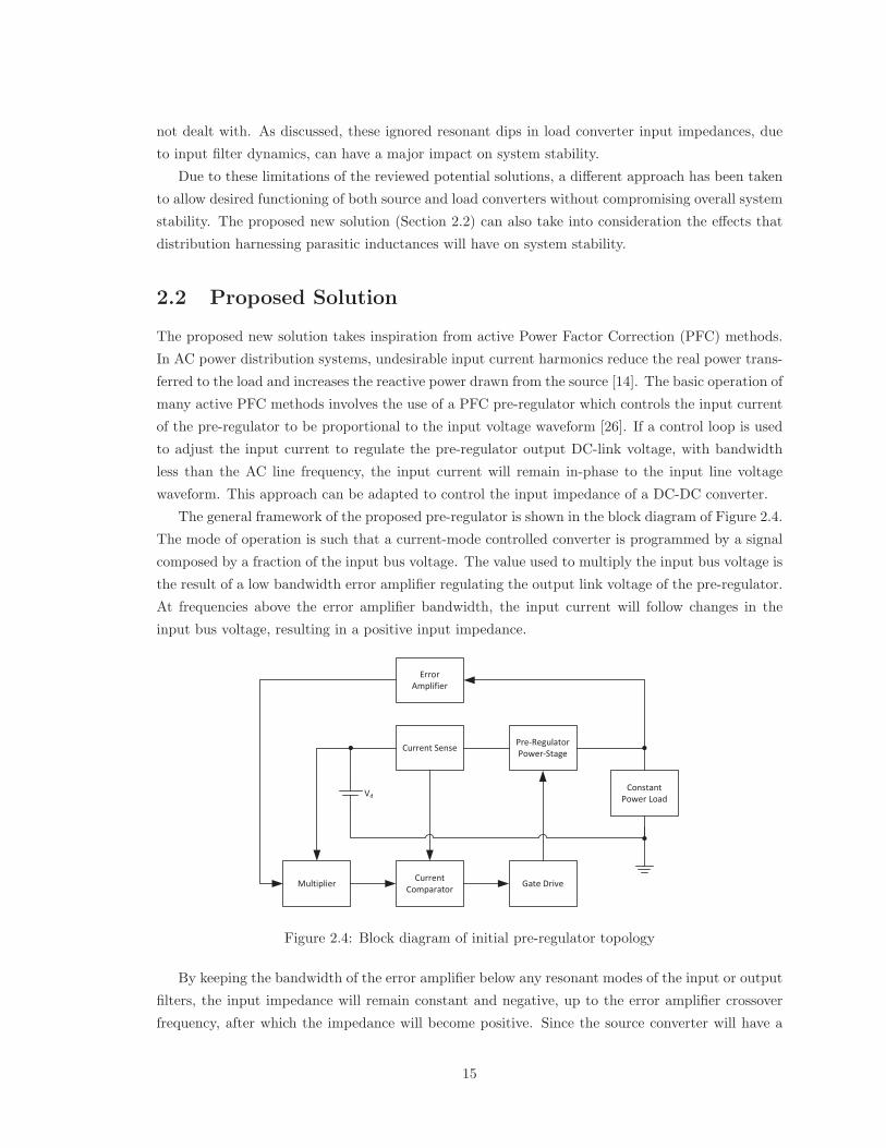
The general framework of the proposed pre-regulator is shown in the block diagram of Figure 2.4.
The mode of operation is such that a current-mode controlled converter is programmed by a signal
composed by a fraction of the input bus voltage. The value used to multiply the input bus voltage is
the result of a low bandwidth error amplifier regulating the output link voltage of the pre-regulator.
At frequencies above the error amplifier bandwidth, the input current will follow changes in the
input bus voltage, resulting in a positive input impedance.
Figure 2.4: Block diagram of initial pre-regulator topology
By keeping the bandwidth of the error amplifier below any resonant modes of the input or output
filters, the input impedance will remain constant and negative, up to the error amplifier crossover
frequency, after which the impedance will become positive. Since the source converter will have a
15

low output impedance at DC, the negative impedance issues at higher frequencies will be avoided.
The load converter loop response can be designed independent of the pre-regulator. In addition, the
source converter loop response will no longer be artificially restricted to ensure proper compatibility
of its input impedance.
Since the load converter is decoupled from the source converter, the dynamics of the cascaded
pre-regulator and load converter can be modelled acting together, to ensure system stability without
either conservative criteria, nor requiring modelling of the entire distributed DC power system. In
order to model the input impedance of the cascaded system with multiple nested feedback loops,
more accurate state space models of current-mode control will be required; these are derived in
Chapter 3. If the pre-regulator is chosen to be a Peak Current-Mode (PCM) (or VCM) controlled
converter then the stability between the two converters becomes easily determined and the time-
averaged input current will closely follow the peak (or valley) inductor current. However, there may
be situations where the pre-regulator converter needs to be constrained to a specific configuration,
therefore the models in Chapter 3 will be derived for all basic converter topologies: Buck, Boost
and Flyback, from which all other derived topologies can be modelled with only minor adjustments.
These new models are used in Chapter 4 to analyse the proposed pre-regulator system.
Since the proposed pre-regulator shapes the input impedance of the cascaded system and is
independent of the source converter control, this approach can be used in conjunction with any of
the system level stability criteria, as discussed in Section 1.1.1.
16
Chapter 3
State Space Modelling of
Current-Mode Control
3.1 Modelling Peak Current-Mode Control
Current-mode control of pulse-width modulated DC-DC converters operates on the premise of turn-
ing the converters power stage into a controlled current source [27]. Most often, in order to regulate
the converter output voltage, a linear control loop is closed around the current-mode controlled
power stage [27]. By controlling the inductor current and not the output capacitor voltage directly,
current-mode control can bring many desirable properties to a power supply designer. In addition to
improving transient response and allowing for the easy implementation of current-limiting protection
circuitry, non-minimum phase systems such as the Boost and Flyback converters can be more easily
controlled, limiting the effects of the right half-plane zeros [28].
While there are many current-mode control methods, the most often employed is constant-
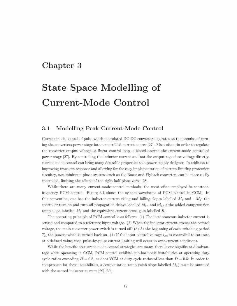
frequency PCM control. Figure 3.1 shows the system waveforms of PCM control in CCM. In
this convention, one has the inductor current rising and falling slopes labelled M1 and −M2; the
controller turn-on and turn-off propagation delays labelled tdon and tdoff ; the added compensation
ramp slope labelled Ma and the equivalent current-sense gain labelled Ri.
The operating principle of PCM control is as follows. (1) The instantaneous inductor current is
sensed and compared to a reference input voltage. (2) When the inductor current crosses the control
voltage, the main converter power switch is turned off. (3) At the beginning of each switching period
Ts, the power switch is turned back on. (4) If the input control voltage ictl is controlled to saturate
at a defined value, then pulse-by-pulse current limiting will occur in over-current conditions.
While the benefits to current-mode control strategies are many, there is one significant disadvan-
tage when operating in CCM; PCM control exhibits sub-harmonic instabilities at operating duty
cycle ratios exceeding D = 0.5, as does VCM at duty cycle ratios of less than D = 0.5. In order to
compensate for these instabilities, a compensation ramp (with slope labelled Ma) must be summed
with the sensed inductor current [29] [30].
17
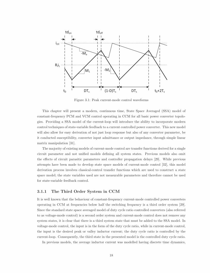
Figure 3.1: Peak current-mode control waveforms
This chapter will present a modern, continuous time, State Space Averaged (SSA) model of
constant-frequency PCM and VCM control operating in CCM for all basic power converter topolo-
gies. Providing a SSA model of the current-loop will introduce the ability to incorporate modern
control techniques of state-variable feedback to a current controlled power converter. This new model
will also allow for easy derivation of not just loop response but also of any converter parameter, be
it conducted susceptibility, converter input admittance or output impedance, through simple linear
matrix manipulation [31].
The majority of existing models of current-mode control are transfer functions derived for a single
circuit parameter and not unified models defining all system states. Previous models also omit
the effects of circuit parasitic parameters and controller propagation delays [29]. While previous
attempts have been made to develop state space models of current-mode control [32], this model
derivation process involves classical-control transfer functions which are used to construct a state
space model; the state variables used are not measurable parameters and therefore cannot be used
for state-variable feedback control.
3.1.1 The Third Order System in CCM
It is well known that the behaviour of constant-frequency current-mode controlled power converters
operating in CCM at frequencies below half the switching frequency is a third order system [29].
Since the standard state space averaged model of duty cycle ratio controlled converters (also referred
to as voltage-mode control) is a second order system and current-mode control does not remove any
system states, it is clear that there is a third system state that must be added to the SSA model. In
voltage-mode control, the input is in the form of the duty cycle ratio, while in current-mode control,
the input is the desired peak or valley inductor current; the duty cycle ratio is controlled by the
current-loop. Consequently, the third state in the presented model is the controlled duty cycle ratio.
In previous models, the average inductor current was modelled having discrete time dynamics,
18
and the average inductor current as a discrete time state [29] [30] [33]. However, the only real state
with discrete time properties is the controlled duty cycle ratio, which can only change values from
one switching period to the next. This choice of state allows for an accurate model to be derived
in which all the system states are circuit parameters which can be physically measured. An added
benefit of choosing measurable circuit parameters as system states is they can, in turn, be used for
state-variable feedback control.
By treating the duty cycle ratio as a system state, the stabilising properties of the compensation
ramp also become more clearly apparent. Figure 3.1 illustrates that the compensation ramp (Ma)
can be modelled simply as state-variable feedback, where the controlled duty cycle ratio is the state
used for the feedback. The change in control signal, at the instant the sensed inductor current
crosses the compensation ramp, subtracted from the control signal, is equal to DMaTs. Therefore
the state-variable feedback gain becomes MaTs. Because of this behaviour, the compensation ramp
will initially be ignored to simplify the derivation process.
Classical control transfer function models of PCM control, such as those presented in [29], suffer
from having to be derived for each input-output pair a circuit designer requires. On the other hand,
the presented SSA model encapsulates all system dynamics into a single representation from which
any parameter, be it loop response, input impedance, output impedance, or conducted susceptibility,
can be determined. In addition, expanding the model to include a closed voltage-loop around the
current-loop, becomes trivial, allowing for the closed-loop input impedance, conducted susceptibility,
and output impedance to be determined with ease. These parameters cannot be determined with
existing classical control models of current-mode control.
3.1.2 Modelling the PCM Controlled Buck Converter
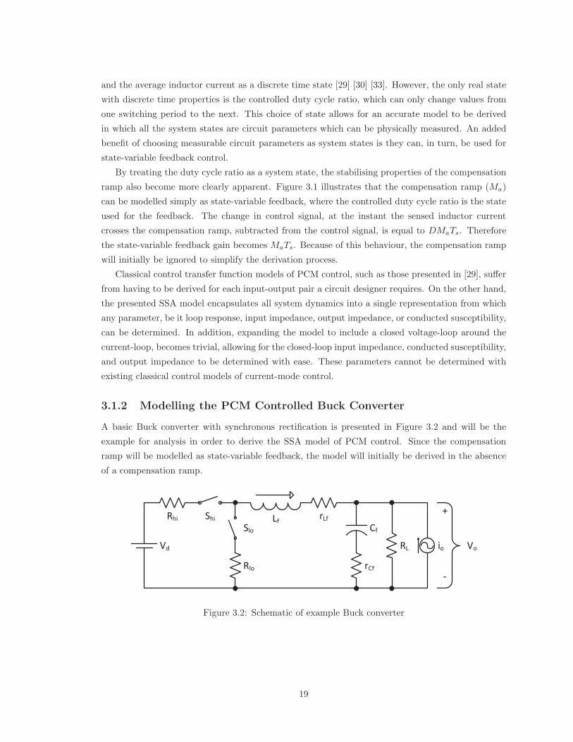
A basic Buck converter with synchronous rectification is presented in Figure 3.2 and will be the
example for analysis in order to derive the SSA model of PCM control. Since the compensation
ramp will be modelled as state-variable feedback, the model will initially be derived in the absence
of a compensation ramp.
Figure 3.2: Schematic of example Buck converter
19
Since PCM control still retains the same power stage structure as that of duty cycle ratio pro-
grammed converters, the SSA model of the duty cycle ratio controlled Buck converter of Figure 3.2
can be given by (3.1) and (3.2), and used as the foundation of the PCM controlled model.
x = Ax+Bu (3.1a)
y = Cx+Du (3.1b)
x =
[iL
vC
], y =
[vout
iin
], u =
⎡⎢⎢⎣vd
d
io
⎤⎥⎥⎦ (3.1c)
A =
⎡⎣−rLf−DRhi−(1−D)Rlo−
RLrCfRL+rCf
Lf
−RL
Lf (RL+rCf )
RL
Cf (RL+rCf )−1
Cf (RL+rCf )
⎤⎦ (3.2a)
B =
[DLf
Vd+IL(Rlo−Rhi)Lf
−RLrCf
Lf (RL+rCf )
0 0 −RL
Cf (RL+rCf )
](3.2b)
C =
[RL
RL+rCf
RLrCf
RL+rCf
D 0
](3.2c)
D =
[0 0
RLrCf
RL+rCf
0 IL 0
](3.2d)
By moving the duty cycle ratio terms from the B matrix in (3.2) to the A matrix for PCM
control, only the third row of the new A and B matrices must be determined. The notation of the
newly defined terms are described in (3.3) and (3.4).
x = Ax+Bu (3.3a)
y = Cx+Du (3.3b)
x =
⎡⎢⎢⎣iL
vC
d
⎤⎥⎥⎦ , y =
[vout
iin
], u =
⎡⎢⎢⎣vd
ictl
io
⎤⎥⎥⎦ (3.3c)
˙d = a3,1iL + a3,2vC + a3,3d+ b3,1vd + b3,2ictl + b3,3io (3.4)
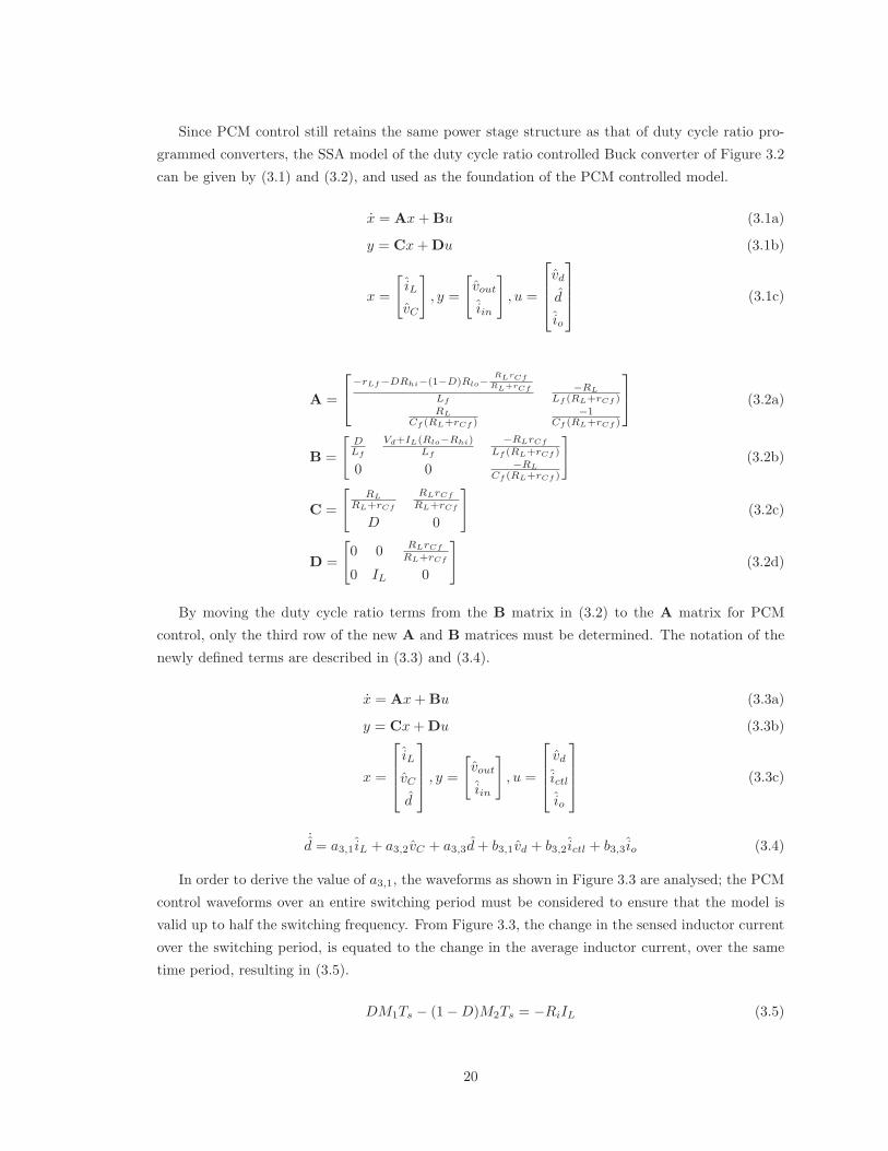
In order to derive the value of a3,1, the waveforms as shown in Figure 3.3 are analysed; the PCM
control waveforms over an entire switching period must be considered to ensure that the model is
valid up to half the switching frequency. From Figure 3.3, the change in the sensed inductor current
over the switching period, is equated to the change in the average inductor current, over the same
time period, resulting in (3.5).
DM1Ts − (1−D)M2Ts = −RiIL (3.5)
20
Figure 3.3: Change in the duty cycle ratio (Δd), over a single switching period, due to small-signalvariations in inductor current (iL)
Taking into consideration the small signal variations in (3.5) alone, gives:
d =−Ri
(M1 +M2)TsiL (3.6)
Because d is a discrete time variable, the change in d over the switching period Ts is defined as
the small signal variation found in (3.6) over Ts, resulting in:
Δd =−Ri
(M1 +M2)T 2s
iL (3.7)
Substituting (3.7) into the a3,1 term of (3.4) directly results in the complex conjugate poles
appearing at frequencies below half the switching frequency. However, it is known that the sub-
harmonic oscillations occur at exactly half the switching frequency [29]. This discrepancy is due
to the discrete time difference equation (3.7) approximating a continuous time differential equation.
Existing classical-control models of PCM have used Pade Approximants to include time-delay effects
of the discrete time nature of the switched inductor current [34]. Because the model is already based
on three state variables, there is no need for the complication of having to use Pade Approximants.
Since the complex conjugate poles must be at exactly half the switching frequency, (3.7) must be
multiplied by the scaling term π2, resulting in:
˙d =
−Riπ2
(M1 +M2)T 2s
iL (3.8)
As in the steps performed above, if the ictl control input signal is perturbed as shown in the
waveforms of Figure 3.4 and scaled by the same π2 term, the derivative of d, and in turn the b3,2
element of (3.4), becomes:
˙d =
π2
(M1 +M2)T 2s
ˆictl (3.9)
21
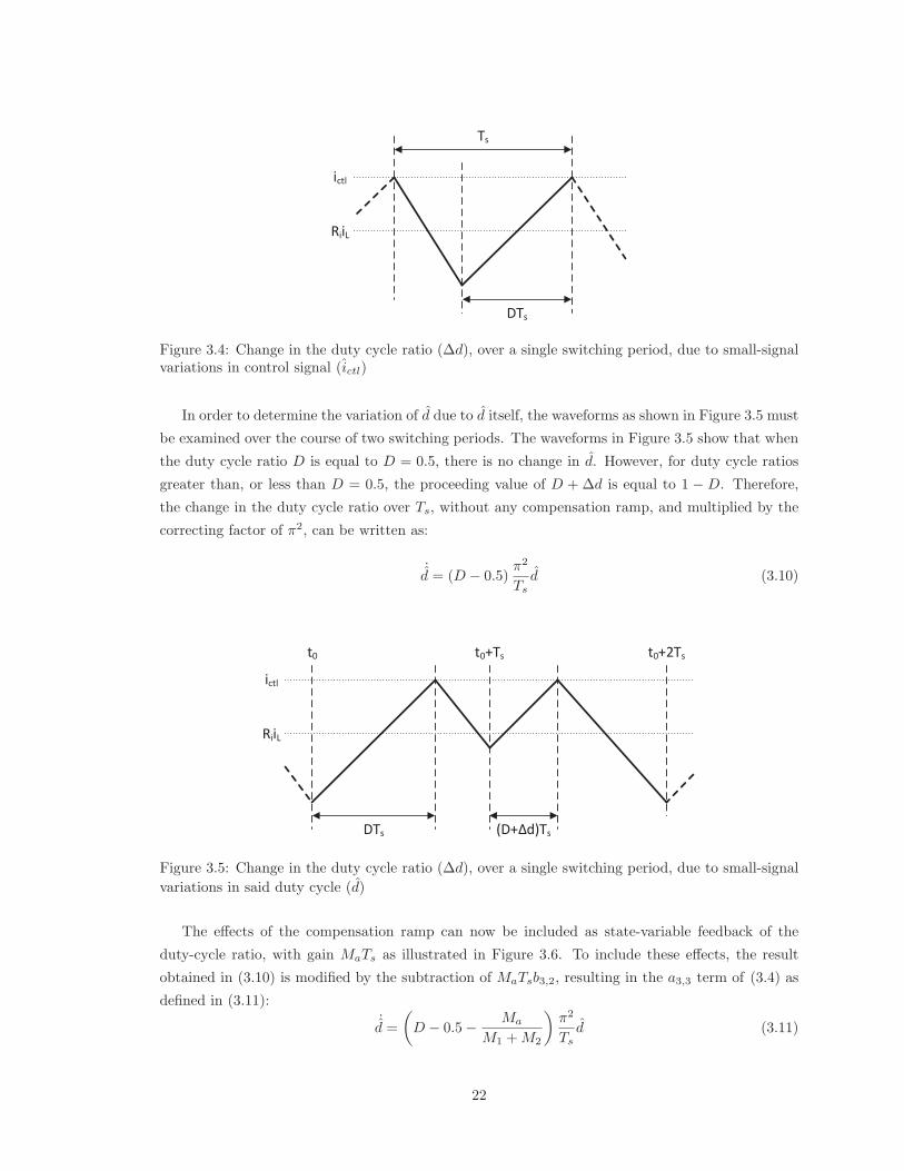
Figure 3.4: Change in the duty cycle ratio (Δd), over a single switching period, due to small-signalvariations in control signal (ictl)
In order to determine the variation of d due to d itself, the waveforms as shown in Figure 3.5 must
be examined over the course of two switching periods. The waveforms in Figure 3.5 show that when
the duty cycle ratio D is equal to D = 0.5, there is no change in d. However, for duty cycle ratios
greater than, or less than D = 0.5, the proceeding value of D + Δd is equal to 1 − D. Therefore,
the change in the duty cycle ratio over Ts, without any compensation ramp, and multiplied by the
correcting factor of π2, can be written as:
˙d = (D − 0.5)
π2
Tsd (3.10)
Figure 3.5: Change in the duty cycle ratio (Δd), over a single switching period, due to small-signal
variations in said duty cycle (d)
The effects of the compensation ramp can now be included as state-variable feedback of the
duty-cycle ratio, with gain MaTs as illustrated in Figure 3.6. To include these effects, the result
obtained in (3.10) is modified by the subtraction of MaTsb3,2, resulting in the a3,3 term of (3.4) as
defined in (3.11):
˙d =
(D − 0.5− Ma
M1 +M2
)π2
Tsd (3.11)
22

Figure 3.6: Equivalent change in control signal due to compensation ramp (Ma)
In the case of the Buck converter, the inductor Lf is always connected to the output capacitor
Cf regardless of switch state. Therefore, variations in output capacitor voltage will not have direct
effects on the duty cycle ratio except for those induced by propagation delays. By examining the
waveforms in Figure 3.7, it can be seen that the controller propagation delay has the same effect
on the operation of PCM as an offset of the ictl signal of tdoffM1. By considering the small-signal
effects of vc only on M1, (3.12) is obtained.
Figure 3.7: Equivalent change in control signal due to propagation delay effects
ictl =−tdoffRi
Lfvc (3.12)
The ictl value obtained in (3.12) can be substituted into (3.9) resulting in the a3,2 term of (3.4)
as described in (3.13).
˙d =
−tdoffRiπ2
Lf (M1 +M2)Ts2 vc (3.13)
23

To derive the b3,1 term, the change in sensed inductor current slope must be included; by following
the methodology for the a3,2 term above, the equivalent change in ictl as a function of vd is given in
(3.14).
ictl =
(tdoffRi
Lf− 0.5RiD(1−D)Ts
Lf
)vd (3.14)
Once again, substituting the ictl value from (3.14) into (3.9) results in the final b3,1 term (3.15).
˙d =
Ri (tdoff − 0.5D(1−D)Ts)π2
Lf (M1 +M2)Ts2 vd (3.15)
Therefore, the final SSA model of the PCM controlled Buck converter is given by (3.3) and (3.16)
through (3.20).
A =
⎡⎢⎢⎣a1,1 a1,2 a1,3
a2,1 a2,2 a2,3
a3,1 a3,2 a3,3
⎤⎥⎥⎦ (3.16a)
a1,1 =−rLf −DRhi − (1−D)Rlo − RLrCf
RL+rCf
Lf(3.16b)
a1,2 =−RL
Lf (RL + rCf )(3.16c)
a1,3 =Vd + IL (Rlo −Rhi)
Lf(3.16d)
a2,1 =RL
Cf (RL + rCf )(3.16e)
a2,2 =−1
Cf (RL + rCf )(3.16f)
a2,3 = 0 (3.16g)
a3,1 =−Riπ
2
(M1 +M2)T 2s
(3.16h)
a3,2 =−tdoffRiπ
2
Lf (M1 +M2)Ts2 (3.16i)
a3,3 =
(D − 0.5− Ma
M1 +M2
)π2
Ts(3.16j)
B =[B1 B2 B3
]=
⎡⎢⎢⎣b1,1 b1,2 b1,3
b2,1 b2,2 b2,3
b3,1 b3,2 b3,3
⎤⎥⎥⎦ (3.17a)
b1,1 =D
Lf(3.17b)
b1,3 =−RLrCf
Lf (RL + rCf )(3.17c)
24

b2,3 =RL
Cf (RL + rCf )(3.17d)
b3,1 =Ri (tdoff − 0.5D(1−D)Ts)π
2
Lf (M1 +M2)Ts2 (3.17e)
b3,2 =π2
(M1 +M2)T 2s
(3.17f)
b1,2 = b2,1 = b3,3 = b2,2 = 0 (3.17g)
C =
[C1
C2
]=
[c1,1 c1,2 c1,3
c2,1 c2,2 c2,3
](3.18a)
c1,1 =RLrCf
RL + rCf(3.18b)
c1,2 =RL
RL + rCf(3.18c)
c2,1 = D (3.18d)
c2,3 = IL (3.18e)
c1,3 = c2,2 = 0 (3.18f)
D =
[0 0
RLrCf
RL+rCf
0 0 0
](3.19a)
M1 = (Vd − Vo − (Rhi + rLf ) IL)Ri
Lf(3.20a)
M2 = (Vo − (Rlo + rLf ) IL)Ri
Lf(3.20b)
3.1.3 Modelling the PCM Controlled Boost Converter
In this section, the previously derived model will be expanded to describe the Boost converter
example shown in Figure 3.8. Since the first two rows of the Boost converter A and B matrices
are determined through the same techniques as the voltage-mode model, all that is required for the
PCM control model are the values of the third rows of the A and B matrices.
The derivative of the duty cycle ratio is a function of terms independent of converter topology,
with the exception of the a3,2 and b3,1 terms of (3.16). Therefore, all other terms for the third
rows of the Boost converter A and B matrices will remain identical to those derived for the Buck
converter. Because the inductor current slopes of the Boost converter differ from those of the Buck
converter, the a3,2 and b3,1 terms, which are dependant on the M1 term, will be different.
25
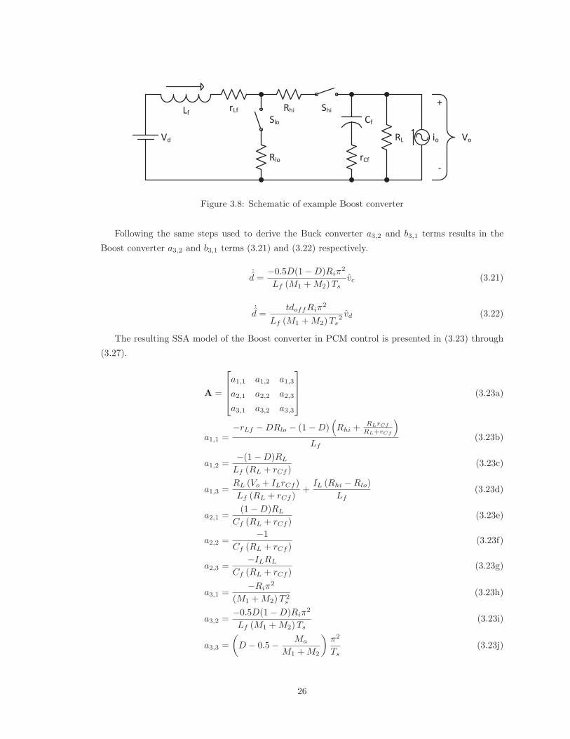
Figure 3.8: Schematic of example Boost converter
Following the same steps used to derive the Buck converter a3,2 and b3,1 terms results in the
Boost converter a3,2 and b3,1 terms (3.21) and (3.22) respectively.
˙d =
−0.5D(1−D)Riπ2
Lf (M1 +M2)Tsvc (3.21)
˙d =
tdoffRiπ2
Lf (M1 +M2)Ts2 vd (3.22)
The resulting SSA model of the Boost converter in PCM control is presented in (3.23) through
(3.27).
A =
⎡⎢⎢⎣a1,1 a1,2 a1,3
a2,1 a2,2 a2,3
a3,1 a3,2 a3,3
⎤⎥⎥⎦ (3.23a)
a1,1 =−rLf −DRlo − (1−D)
(Rhi +
RLrCf
RL+rCf
)Lf
(3.23b)
a1,2 =−(1−D)RL
Lf (RL + rCf )(3.23c)
a1,3 =RL (Vo + ILrCf )
Lf (RL + rCf )+
IL (Rhi −Rlo)
Lf(3.23d)
a2,1 =(1−D)RL
Cf (RL + rCf )(3.23e)
a2,2 =−1
Cf (RL + rCf )(3.23f)
a2,3 =−ILRL
Cf (RL + rCf )(3.23g)
a3,1 =−Riπ
2
(M1 +M2)T 2s
(3.23h)
a3,2 =−0.5D(1−D)Riπ
2
Lf (M1 +M2)Ts(3.23i)
a3,3 =
(D − 0.5− Ma
M1 +M2
)π2
Ts(3.23j)
26

B =[B1 B2 B3
]=
⎡⎢⎢⎣b1,1 b1,2 b1,3
b2,1 b2,2 b2,3
b3,1 b3,2 b3,3
⎤⎥⎥⎦ (3.24a)
b1,1 =1
Lf(3.24b)
b2,3 =RL
Cf (RL + rCf )(3.24c)
b3,1 =tdoffRiπ
2
Lf (M1 +M2)Ts2 (3.24d)
b3,2 =π2
(M1 +M2)T 2s
(3.24e)
b1,2 = b1,3 = b2,1 = b2,2 = b3,3 = 0 (3.24f)
C =
[C1
C2
]=
[c1,1 c1,2 c1,3
c2,1 c2,2 c2,3
](3.25a)
c1,1 =(1−D)RLrCf
RL + rCf(3.25b)
c1,2 =RL
RL + rCf(3.25c)
c1,3 =−ILRLrCf
RL + rCf(3.25d)
c2,1 = 1 (3.25e)
c2,2 = c2,3 = 0 (3.25f)
D =
[0 0
RLrCf
RL+rCf
0 0 0
](3.26a)
M1 = (Vd − (rLf +Rlo) IL)Ri
Lf(3.27a)
M2 = (Vo − Vd − (rLf +Rhi) IL)Ri
Lf(3.27b)
3.1.4 Modelling the PCM Controlled Flyback Converter
In this section, the previously derived model will be expanded to the Flyback converter as shown
in Figure 3.9. In this case, the primary side Flyback transformer series resistance is summed with
the primary side switch on-state resistance to yield Rpri; the secondary winding series resistance
27
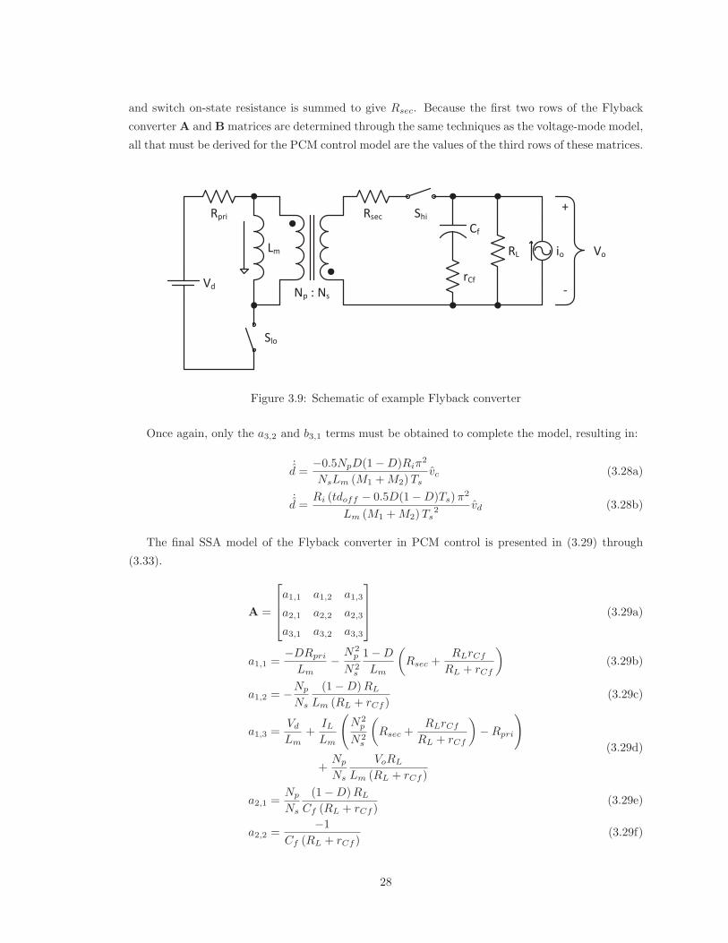
and switch on-state resistance is summed to give Rsec. Because the first two rows of the Flyback
converter A and B matrices are determined through the same techniques as the voltage-mode model,
all that must be derived for the PCM control model are the values of the third rows of these matrices.
Figure 3.9: Schematic of example Flyback converter
Once again, only the a3,2 and b3,1 terms must be obtained to complete the model, resulting in:
˙d =
−0.5NpD(1−D)Riπ2
NsLm (M1 +M2)Tsvc (3.28a)
˙d =
Ri (tdoff − 0.5D(1−D)Ts)π2
Lm (M1 +M2)Ts2 vd (3.28b)
The final SSA model of the Flyback converter in PCM control is presented in (3.29) through
(3.33).
A =
⎡⎢⎢⎣a1,1 a1,2 a1,3
a2,1 a2,2 a2,3
a3,1 a3,2 a3,3
⎤⎥⎥⎦ (3.29a)
a1,1 =−DRpri
Lm− N2
p
N2s
1−D
Lm
(Rsec +
RLrCf
RL + rCf
)(3.29b)
a1,2 = −Np
Ns
(1−D)RL
Lm (RL + rCf )(3.29c)
a1,3 =Vd
Lm+
ILLm
(N2
p
N2s
(Rsec +
RLrCf
RL + rCf
)−Rpri
)
+Np
Ns
VoRL
Lm (RL + rCf )
(3.29d)
a2,1 =Np
Ns
(1−D)RL
Cf (RL + rCf )(3.29e)
a2,2 =−1
Cf (RL + rCf )(3.29f)
28
a2,3 =Np
Ns
−ILRL
Cf (RL + rCf )(3.29g)
a3,1 =−Riπ
2
(M1 +M2)T 2s
(3.29h)
a3,2 =−0.5NpD(1−D)Riπ
2
NsLm (M1 +M2)Ts(3.29i)
a3,3 =
(D − 0.5− Ma
M1 +M2
)π2
Ts(3.29j)
B =[B1 B2 B3
]=
⎡⎢⎢⎣b1,1 b1,2 b1,3
b2,1 b2,2 b2,3
b3,1 b3,2 b3,3
⎤⎥⎥⎦ (3.30a)
b1,1 =D
Lm(3.30b)
b1,3 = −Np
Ns
(1−D)RLrCf
Lm (RL + rCf )(3.30c)
b2,3 =RL
Cf (RL + rCf )(3.30d)
b3,1 =Ri (tdoff − 0.5D(1−D)Ts)π
2
Lm (M1 +M2)Ts2 (3.30e)
b3,2 =π2
(M1 +M2)T 2s
(3.30f)
b1,2 = b2,1 = b2,2 = b3,3 = 0 (3.30g)
C =
[C1
C2
]=
[c1,1 c1,2 c1,3
c2,1 c2,2 c2,3
](3.31a)
c1,1 =Np
Ns
(1−D)RLrCf
RL + rCf(3.31b)
c1,2 =RL
RL + rCf(3.31c)
c1,3 = −Np
Ns
ILRLrCf
RL + rCf(3.31d)
c2,1 = D (3.31e)
c2,2 = 0 (3.31f)
c2,3 = IL (3.31g)
D =
[0 0
RLrCf
RL+rCf
0 0 0
](3.32a)
29
M1 = (Vd − ILRpri)Ri
Lm(3.33a)
M2 =Np
Ns
(Vo − Np
NsILRsec
)Ri
Lm(3.33b)
3.2 Experimental Verification of the PCM Models
Before the SSA model can be used to design the pre-regulator loops and perform accurate stability
analysis (see Chapter 4), the models derived in Sections 3.1.2 through 3.1.3 will be compared to
measured Bode plots of various converter parameters obtained from prototype Buck, Boost and
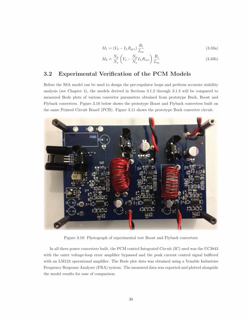
Flyback converters. Figure 3.10 below shows the prototype Boost and Flyback converters built on
the same Printed Circuit Board (PCB). Figure 3.11 shows the prototype Buck converter circuit.
Figure 3.10: Photograph of experimental test Boost and Flyback converters
In all three power converters built, the PCM control Integrated Circuit (IC) used was the UC3843
with the outer voltage-loop error amplifier bypassed and the peak current control signal buffered
with an LM124 operational amplifier. The Bode plot data was obtained using a Venable Industries
Frequency Response Analyser (FRA) system. The measured data was exported and plotted alongside
the model results for ease of comparison.
30
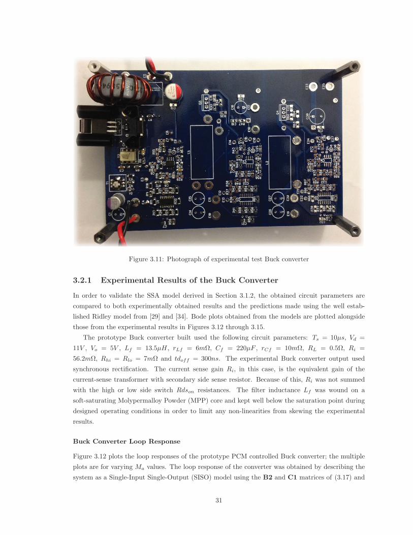
Figure 3.11: Photograph of experimental test Buck converter
3.2.1 Experimental Results of the Buck Converter
In order to validate the SSA model derived in Section 3.1.2, the obtained circuit parameters are
compared to both experimentally obtained results and the predictions made using the well estab-
lished Ridley model from [29] and [34]. Bode plots obtained from the models are plotted alongside
those from the experimental results in Figures 3.12 through 3.15.
The prototype Buck converter built used the following circuit parameters: Ts = 10μs, Vd =
11V , Vo = 5V , Lf = 13.5μH, rLf = 6mΩ, Cf = 220μF , rCf = 10mΩ, RL = 0.5Ω, Ri =
56.2mΩ, Rhi = Rlo = 7mΩ and tdoff = 300ns. The experimental Buck converter output used
synchronous rectification. The current sense gain Ri, in this case, is the equivalent gain of the
current-sense transformer with secondary side sense resistor. Because of this, Ri was not summed
with the high or low side switch Rdson resistances. The filter inductance Lf was wound on a
soft-saturating Molypermalloy Powder (MPP) core and kept well below the saturation point during
designed operating conditions in order to limit any non-linearities from skewing the experimental
results.
Buck Converter Loop Response
Figure 3.12 plots the loop responses of the prototype PCM controlled Buck converter; the multiple
plots are for varying Ma values. The loop response of the converter was obtained by describing the
system as a Single-Input Single-Output (SISO) model using the B2 and C1 matrices of (3.17) and
31
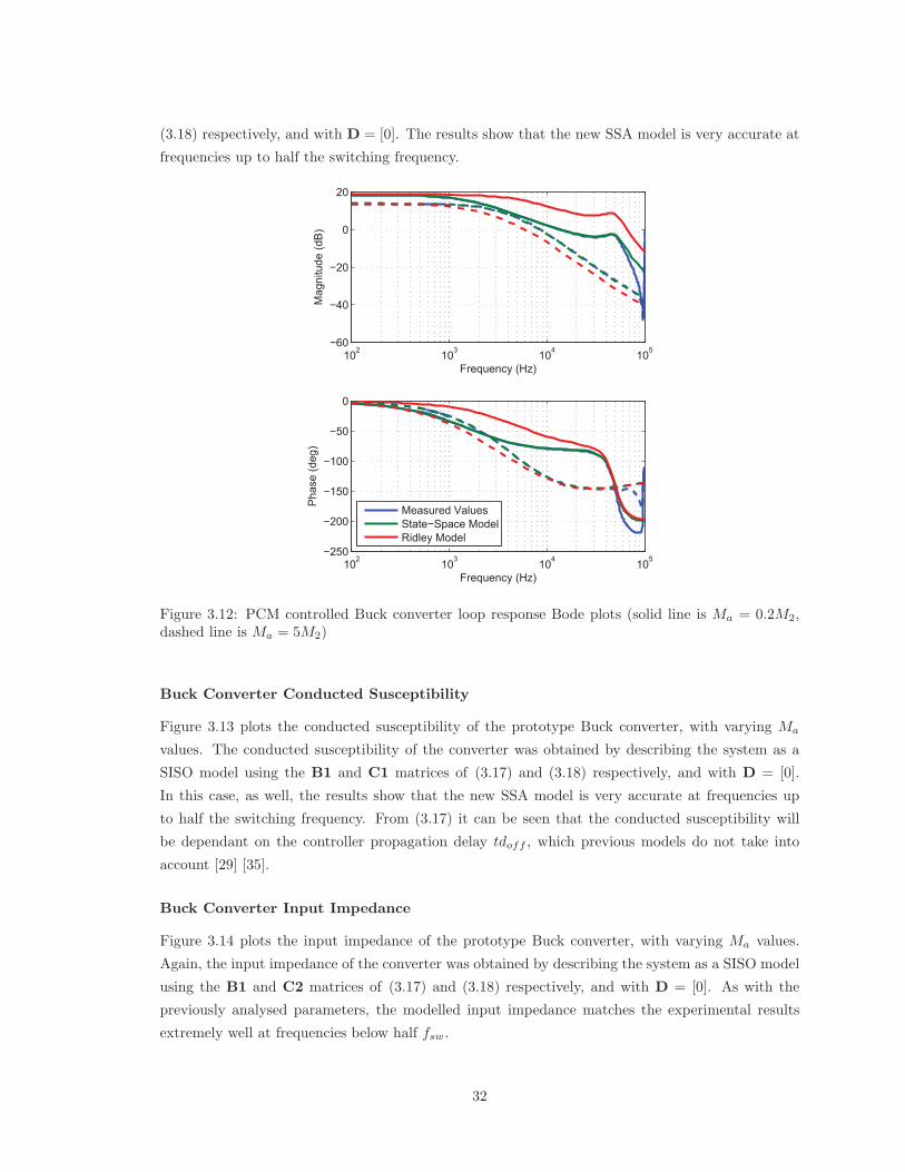
(3.18) respectively, and with D = [0]. The results show that the new SSA model is very accurate at
frequencies up to half the switching frequency.
102 103 104 105−60
−40
−20
0
20
Mag
nitu
de (d
B)
Frequency (Hz)
102 103 104 105−250
−200
−150
−100
−50
0
Pha
se (d
eg)
Frequency (Hz)
Measured ValuesState−Space ModelRidley Model
Figure 3.12: PCM controlled Buck converter loop response Bode plots (solid line is Ma = 0.2M2,dashed line is Ma = 5M2)
Buck Converter Conducted Susceptibility
Figure 3.13 plots the conducted susceptibility of the prototype Buck converter, with varying Ma
values. The conducted susceptibility of the converter was obtained by describing the system as a
SISO model using the B1 and C1 matrices of (3.17) and (3.18) respectively, and with D = [0].
In this case, as well, the results show that the new SSA model is very accurate at frequencies up
to half the switching frequency. From (3.17) it can be seen that the conducted susceptibility will
be dependant on the controller propagation delay tdoff , which previous models do not take into
account [29] [35].
Buck Converter Input Impedance
Figure 3.14 plots the input impedance of the prototype Buck converter, with varying Ma values.
Again, the input impedance of the converter was obtained by describing the system as a SISO model
using the B1 and C2 matrices of (3.17) and (3.18) respectively, and with D = [0]. As with the
previously analysed parameters, the modelled input impedance matches the experimental results
extremely well at frequencies below half fsw.
32
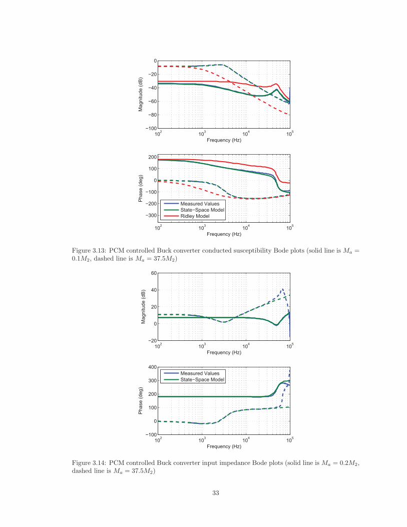
102 103 104 105−100
−80
−60
−40
−20
0
Mag
nitu
de (d
B)
Frequency (Hz)
102 103 104 105
−300
−200
−100
0
100
200
Pha
se (d
eg)
Frequency (Hz)
Measured ValuesState−Space ModelRidley Model
Figure 3.13: PCM controlled Buck converter conducted susceptibility Bode plots (solid line is Ma =0.1M2, dashed line is Ma = 37.5M2)
102 103 104 105−20
0
20
40
60
Mag
nitu
de (d
B)
Frequency (Hz)
102 103 104 105−100
0
100
200
300
400
Pha
se (d
eg)
Frequency (Hz)
Measured ValuesState−Space Model
Figure 3.14: PCM controlled Buck converter input impedance Bode plots (solid line is Ma = 0.2M2,dashed line is Ma = 37.5M2)
33
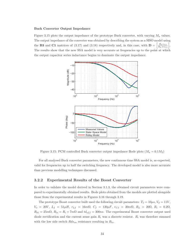
Buck Converter Output Impedance
Figure 3.15 plots the output impedance of the prototype Buck converter, with varying Ma values.
The output impedance of the converter was obtained by describing the system as a SISO model using
the B3 and C1 matrices of (3.17) and (3.18) respectively and, in this case, with D =[
RLrCf
RL+rCf
].
The results show that the new SSA model is very accurate at frequencies up to the point at which
the output capacitor series inductance begins to dominate the output impedance.
102 103 104 105
−40
−30
−20
−10M
agni
tude
(dB
)
Frequency (Hz)
102 103 104 105
−100
−50
0
Pha
se (d
eg)
Frequency (Hz)
Measured ValuesState−Space ModelRidley Model
Figure 3.15: PCM controlled Buck converter output impedance Bode plots (Ma = 0.1M2)
For all analysed Buck converter parameters, the new continuous time SSA model is, as expected,
valid for frequencies up to half the switching frequency. The developed model is also more accurate
than previous modelling techniques discussed.
3.2.2 Experimental Results of the Boost Converter
In order to validate the model derived in Section 3.1.3, the obtained circuit parameters were com-
pared to experimentally obtained results. Bode plots obtained from the models are plotted alongside
those from the experimental results in Figures 3.16 through 3.19.
The prototype Boost converter built used the following circuit parameters: Ts = 10μs, Vd = 11V ,
Vo = 20V , Lf = 51μH, rLf = 16mΩ, Cf = 120μF , rCf = 20mΩ, RL = 20Ω, Ri = 0.2Ω,
Rhi = 25mΩ, Rlo = Ri + 7mΩ and tdoff = 300ns. The experimental Boost converter output used
diode rectification and the current sense gain Ri was a discrete resistor. Ri was therefore summed
with the low side switch Rdson resistance resulting in Rlo.
34
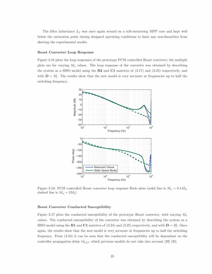
The filter inductance Lf was once again wound on a soft-saturating MPP core and kept well
below the saturation point during designed operating conditions to limit any non-linearities from
skewing the experimental results.
Boost Converter Loop Response
Figure 3.16 plots the loop responses of the prototype PCM controlled Boost converter; the multiple
plots are for varying Ma values. The loop response of the converter was obtained by describing
the system as a SISO model using the B2 and C1 matrices of (3.17) and (3.25) respectively, and
with D = [0]. The results show that the new model is very accurate at frequencies up to half the
switching frequency.
102 103 104 105−40
−30
−20
−10
0
10
20
30
Mag
nitu
de (d
B)
Frequency (Hz)
102 103 104 105−300
−250
−200
−150
−100
−50
0
Pha
se (d
eg)
Frequency (Hz)
Measured ValuesState−Space Model
Figure 3.16: PCM controlled Boost converter loop response Bode plots (solid line is Ma = 0.1M2,dashed line is Ma = 2M2)
Boost Converter Conducted Susceptibility
Figure 3.17 plots the conducted susceptibility of the prototype Boost converter, with varying Ma
values. The conducted susceptibility of the converter was obtained by describing the system as a
SISO model using the B1 and C1 matrices of (3.24) and (3.25) respectively, and with D = [0]. Once
again, the results show that the new model is very accurate at frequencies up to half the switching
frequency. From (3.24) it can be seen that the conducted susceptibility will be dependant on the
controller propagation delay tdoff , which previous models do not take into account [29] [35].
35
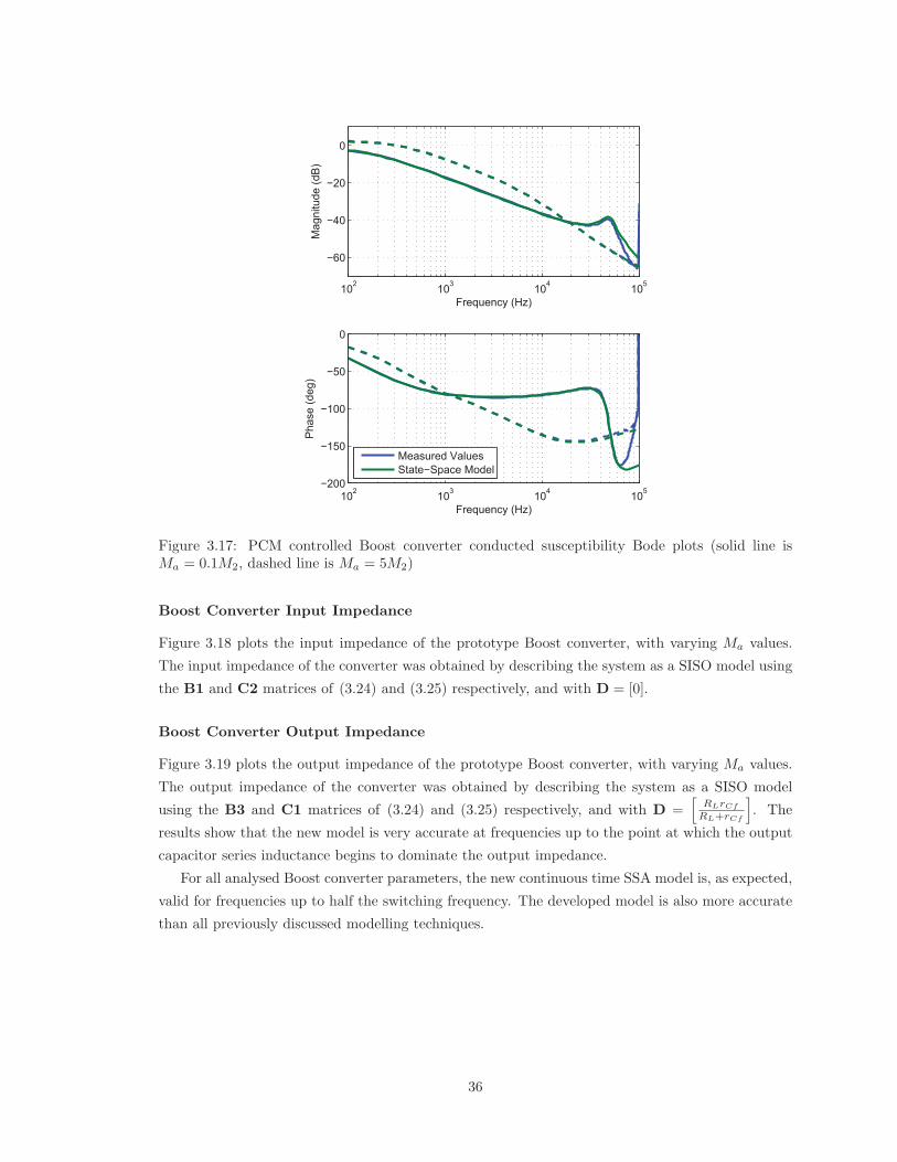
102 103 104 105
−60
−40
−20
0
Mag
nitu
de (d
B)
Frequency (Hz)
102 103 104 105−200
−150
−100
−50
0
Pha
se (d
eg)
Frequency (Hz)
Measured ValuesState−Space Model
Figure 3.17: PCM controlled Boost converter conducted susceptibility Bode plots (solid line isMa = 0.1M2, dashed line is Ma = 5M2)
Boost Converter Input Impedance
Figure 3.18 plots the input impedance of the prototype Boost converter, with varying Ma values.
The input impedance of the converter was obtained by describing the system as a SISO model using
the B1 and C2 matrices of (3.24) and (3.25) respectively, and with D = [0].
Boost Converter Output Impedance
Figure 3.19 plots the output impedance of the prototype Boost converter, with varying Ma values.
The output impedance of the converter was obtained by describing the system as a SISO model
using the B3 and C1 matrices of (3.24) and (3.25) respectively, and with D =[
RLrCf
RL+rCf
]. The
results show that the new model is very accurate at frequencies up to the point at which the output
capacitor series inductance begins to dominate the output impedance.
For all analysed Boost converter parameters, the new continuous time SSA model is, as expected,
valid for frequencies up to half the switching frequency. The developed model is also more accurate
than all previously discussed modelling techniques.
36
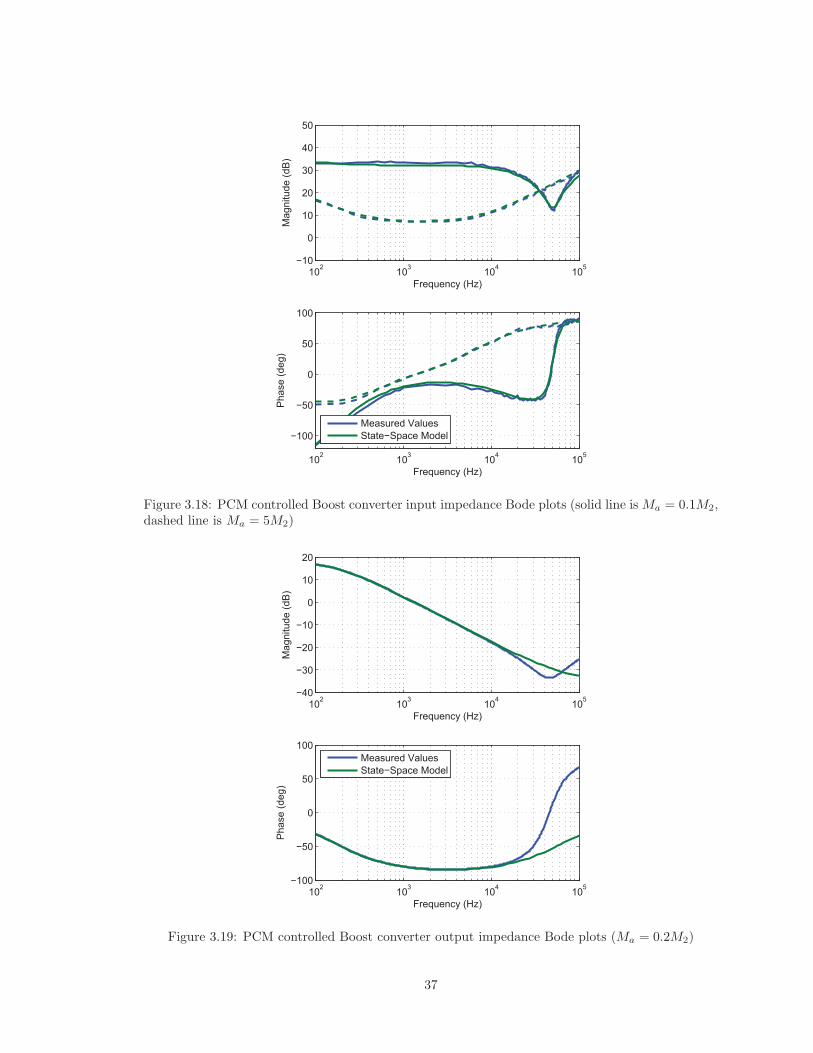
102 103 104 105−10
0
10
20
30
40
50
Mag
nitu
de (d
B)
Frequency (Hz)
102 103 104 105
−100
−50
0
50
100
Pha
se (d
eg)
Frequency (Hz)
Measured ValuesState−Space Model
Figure 3.18: PCM controlled Boost converter input impedance Bode plots (solid line is Ma = 0.1M2,dashed line is Ma = 5M2)
102 103 104 105−40
−30
−20
−10
0
10
20
Mag
nitu
de (d
B)
Frequency (Hz)
102 103 104 105−100
−50
0
50
100
Pha
se (d
eg)
Frequency (Hz)
Measured ValuesState−Space Model
Figure 3.19: PCM controlled Boost converter output impedance Bode plots (Ma = 0.2M2)
37
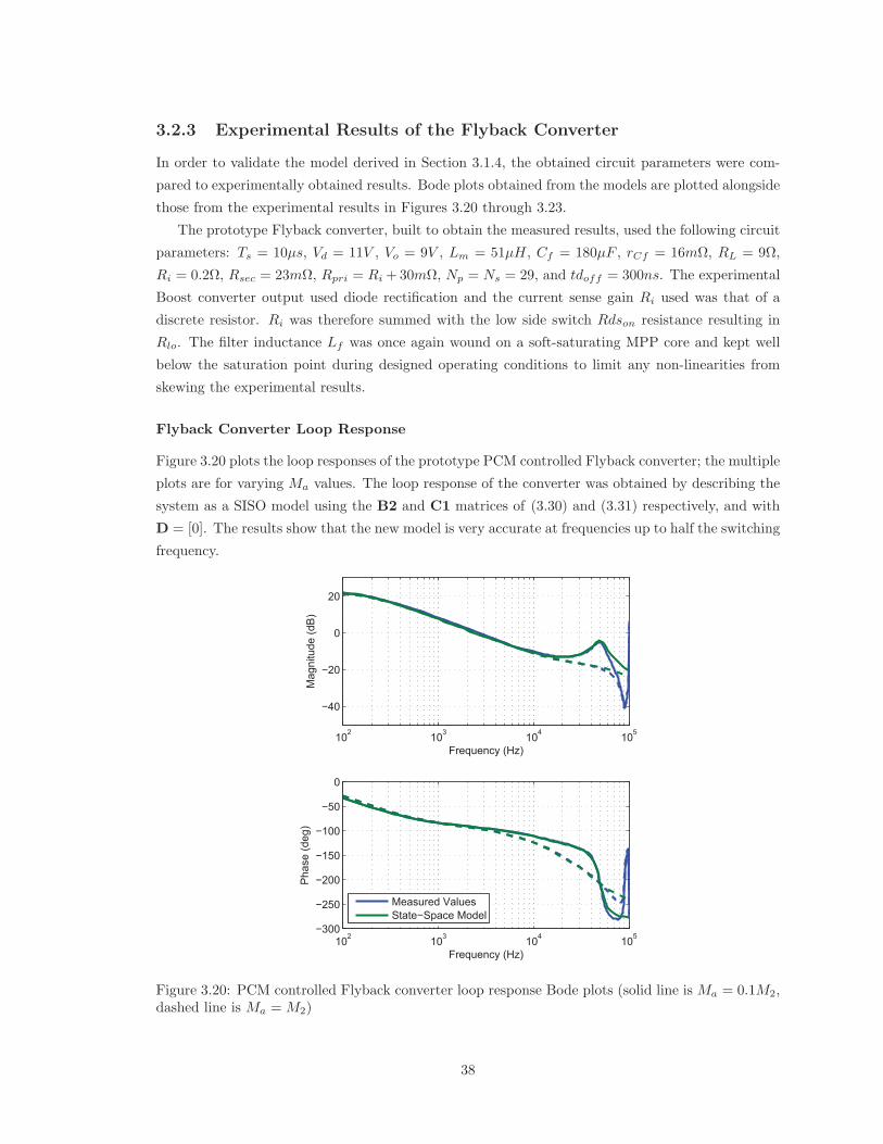
3.2.3 Experimental Results of the Flyback Converter
In order to validate the model derived in Section 3.1.4, the obtained circuit parameters were com-
pared to experimentally obtained results. Bode plots obtained from the models are plotted alongside
those from the experimental results in Figures 3.20 through 3.23.
The prototype Flyback converter, built to obtain the measured results, used the following circuit
parameters: Ts = 10μs, Vd = 11V , Vo = 9V , Lm = 51μH, Cf = 180μF , rCf = 16mΩ, RL = 9Ω,
Ri = 0.2Ω, Rsec = 23mΩ, Rpri = Ri +30mΩ, Np = Ns = 29, and tdoff = 300ns. The experimental
Boost converter output used diode rectification and the current sense gain Ri used was that of a
discrete resistor. Ri was therefore summed with the low side switch Rdson resistance resulting in
Rlo. The filter inductance Lf was once again wound on a soft-saturating MPP core and kept well
below the saturation point during designed operating conditions to limit any non-linearities from
skewing the experimental results.
Flyback Converter Loop Response
Figure 3.20 plots the loop responses of the prototype PCM controlled Flyback converter; the multiple
plots are for varying Ma values. The loop response of the converter was obtained by describing the
system as a SISO model using the B2 and C1 matrices of (3.30) and (3.31) respectively, and with
D = [0]. The results show that the new model is very accurate at frequencies up to half the switching
frequency.
102 103 104 105
−40
−20
0
20
Mag
nitu
de (d
B)
Frequency (Hz)
102 103 104 105−300
−250
−200
−150
−100
−50
0
Pha
se (d
eg)
Frequency (Hz)
Measured ValuesState−Space Model
Figure 3.20: PCM controlled Flyback converter loop response Bode plots (solid line is Ma = 0.1M2,dashed line is Ma = M2)
38

Flyback Converter Conducted Susceptibility
Figure 3.21 plots the conducted susceptibility of the prototype Flyback converter, with varying Ma
values. The conducted susceptibility of the converter was obtained by describing the system as a
SISO model using the B1 and C1 matrices of (3.30) and (3.31) respectively, and with D = [0]. Once
again, the results show that the new model is very accurate at frequencies up to half the switching
frequency. From (3.30) it can be seen that the conducted susceptibility will be dependant on the
controller propagation delay tdoff , which previous models do not take into account [35] [29].
102 103 104 105−80
−60
−40
−20
0M
agni
tude
(dB
)
Frequency (Hz)
102 103 104 105−200
−150
−100
−50
0
Pha
se (d
eg)
Frequency (Hz)
Measured ValuesState−Space Model
Figure 3.21: PCM controlled Flyback converter conducted susceptibility Bode plots (solid line isMa = 0.2M2, dashed line is Ma = 5M2)
Flyback Converter Input Impedance
Figure 3.22 plots the input impedance of the prototype Flyback converter, with varying Ma values.
The input impedance of the converter was obtained by describing the system as a SISO model using
the B1 and C2 matrices of (3.30) and (3.31) respectively, and with D = [0].
Flyback Converter Output Impedance
Figure 3.23 plots the output impedance of the prototype Flyback converter, with varying Ma values.
The output impedance of the converter was obtained by describing the system as a SISO model
using the B3 and C1 matrices of (3.30) and (3.31) respectively, and with D =[
RLrCf
RL+rCf
].
39
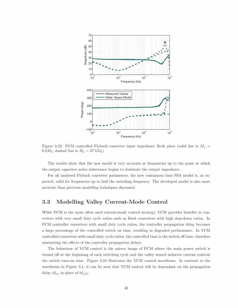
102 103 104 1050
10
20
30
40
50
60
70
Mag
nitu
de (d
B)
Frequency (Hz)
102 103 104 105−100
0
100
200
300
400
Pha
se (d
eg)
Frequency (Hz)
Measured ValuesState−Space Model
Figure 3.22: PCM controlled Flyback converter input impedance Bode plots (solid line is Ma =0.2M2, dashed line is Ma = 37.5M2)
The results show that the new model is very accurate at frequencies up to the point at which
the output capacitor series inductance begins to dominate the output impedance.
For all analysed Flyback converter parameters, the new continuous time SSA model is, as ex-
pected, valid for frequencies up to half the switching frequency. The developed model is also more
accurate than previous modelling techniques discussed.
3.3 Modelling Valley Current-Mode Control
While PCM is the most often used current-mode control strategy, VCM provides benefits in con-
verters with very small duty cycle ratios such as Buck converters with high step-down ratios. In
PCM controller converters with small duty cycle ratios, the controller propagation delay becomes
a large percentage of the controlled switch on time, resulting in degraded performance. In VCM
controlled converters with small duty cycle ratios, the controlled time is the switch off time, therefore
minimizing the effects of the controller propagation delays.
The behaviour of VCM control is the mirror image of PCM where the main power switch is
turned off at the beginning of each switching cycle and the valley sensed inductor current controls
the switch turn-on time. Figure 3.24 illustrates the VCM control waveforms. In contrast to the
waveforms in Figure 3.1, it can be seen that VCM control will be dependant on the propagation
delay tdon in place of tdoff .
40
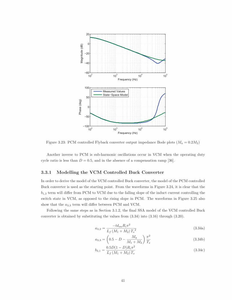
102 103 104 105−60
−40
−20
0
20
Mag
nitu
de (d
B)
Frequency (Hz)
102 103 104 105−100
−50
0
50
100
Pha
se (d
eg)
Frequency (Hz)
Measured ValuesState−Space Model
Figure 3.23: PCM controlled Flyback converter output impedance Bode plots (Ma = 0.2M2)
Another inverse to PCM is sub-harmonic oscillations occur in VCM when the operating duty
cycle ratio is less than D = 0.5, and in the absence of a compensation ramp [36].
3.3.1 Modelling the VCM Controlled Buck Converter
In order to derive the model of the VCM controlled Buck converter, the model of the PCM controlled
Buck converter is used as the starting point. From the waveforms in Figure 3.24, it is clear that the
b1,3 term will differ from PCM to VCM due to the falling slope of the induct current controlling the
switch state in VCM, as opposed to the rising slope in PCM. The waveforms in Figure 3.25 also
show that the a3,3 term will differ between PCM and VCM.
Following the same steps as in Section 3.1.2, the final SSA model of the VCM controlled Buck
converter is obtained by substituting the values from (3.34) into (3.16) through (3.20).
a3,2 =−tdonRiπ
2
Lf (M1 +M2)Ts2 (3.34a)
a3,3 =
(0.5−D − Ma
M1 +M2
)π2
Ts(3.34b)
b3,1 =0.5D(1−D)Riπ
2
Lf (M1 +M2)Ts(3.34c)
41

Figure 3.24: Valley current-mode control waveforms in CCM
Figure 3.25: Sub-harmonic oscillation in VCM
42
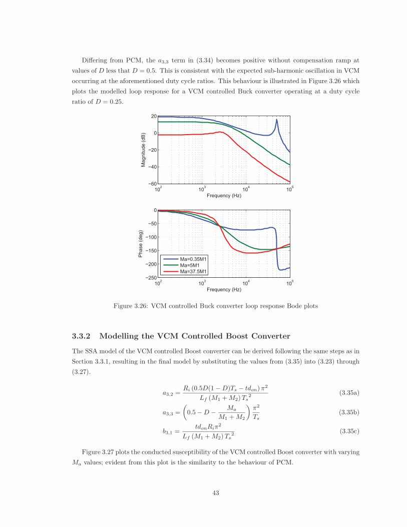
Differing from PCM, the a3,3 term in (3.34) becomes positive without compensation ramp at
values of D less that D = 0.5. This is consistent with the expected sub-harmonic oscillation in VCM
occurring at the aforementioned duty cycle ratios. This behaviour is illustrated in Figure 3.26 which
plots the modelled loop response for a VCM controlled Buck converter operating at a duty cycle
ratio of D = 0.25.
102 103 104 105−60
−40
−20
0
20
Mag
nitu
de (d
B)
Frequency (Hz)
102 103 104 105−250
−200
−150
−100
−50
0
Pha
se (d
eg)
Frequency (Hz)
Ma=0.35M1Ma=5M1Ma=37.5M1
Figure 3.26: VCM controlled Buck converter loop response Bode plots
3.3.2 Modelling the VCM Controlled Boost Converter
The SSA model of the VCM controlled Boost converter can be derived following the same steps as in
Section 3.3.1, resulting in the final model by substituting the values from (3.35) into (3.23) through
(3.27).
a3,2 =Ri (0.5D(1−D)Ts − tdon)π
2
Lf (M1 +M2)Ts2 (3.35a)
a3,3 =
(0.5−D − Ma
M1 +M2
)π2
Ts(3.35b)
b3,1 =tdonRiπ
2
Lf (M1 +M2)Ts2 (3.35c)
Figure 3.27 plots the conducted susceptibility of the VCM controlled Boost converter with varying
Ma values; evident from this plot is the similarity to the behaviour of PCM.
43
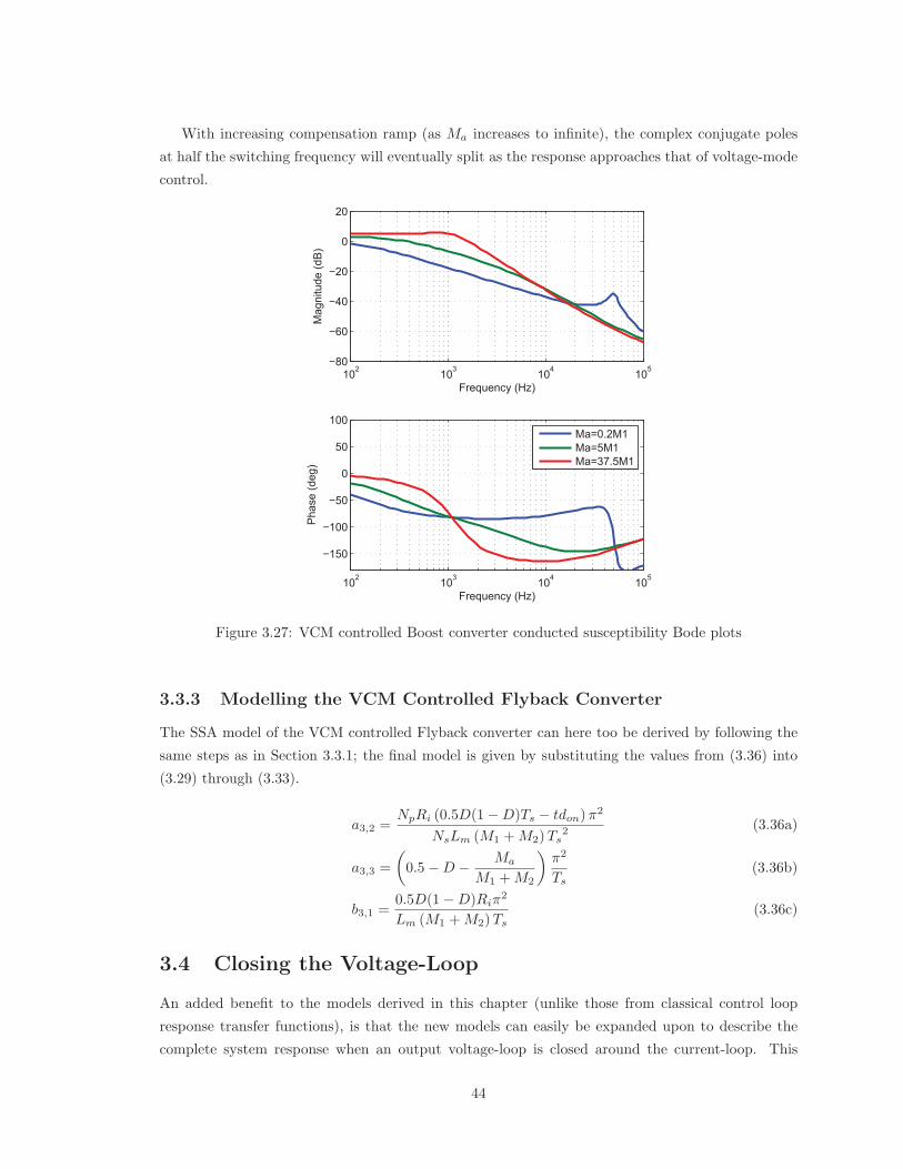
With increasing compensation ramp (as Ma increases to infinite), the complex conjugate poles
at half the switching frequency will eventually split as the response approaches that of voltage-mode
control.
102 103 104 105−80
−60
−40
−20
0
20
Mag
nitu
de (d
B)
Frequency (Hz)
102 103 104 105
−150
−100
−50
0
50
100
Pha
se (d
eg)
Frequency (Hz)
Ma=0.2M1Ma=5M1Ma=37.5M1
Figure 3.27: VCM controlled Boost converter conducted susceptibility Bode plots
3.3.3 Modelling the VCM Controlled Flyback Converter
The SSA model of the VCM controlled Flyback converter can here too be derived by following the
same steps as in Section 3.3.1; the final model is given by substituting the values from (3.36) into
(3.29) through (3.33).
a3,2 =NpRi (0.5D(1−D)Ts − tdon)π
2
NsLm (M1 +M2)Ts2 (3.36a)
a3,3 =
(0.5−D − Ma
M1 +M2
)π2
Ts(3.36b)
b3,1 =0.5D(1−D)Riπ
2
Lm (M1 +M2)Ts(3.36c)
3.4 Closing the Voltage-Loop
An added benefit to the models derived in this chapter (unlike those from classical control loop
response transfer functions), is that the new models can easily be expanded upon to describe the
complete system response when an output voltage-loop is closed around the current-loop. This
44
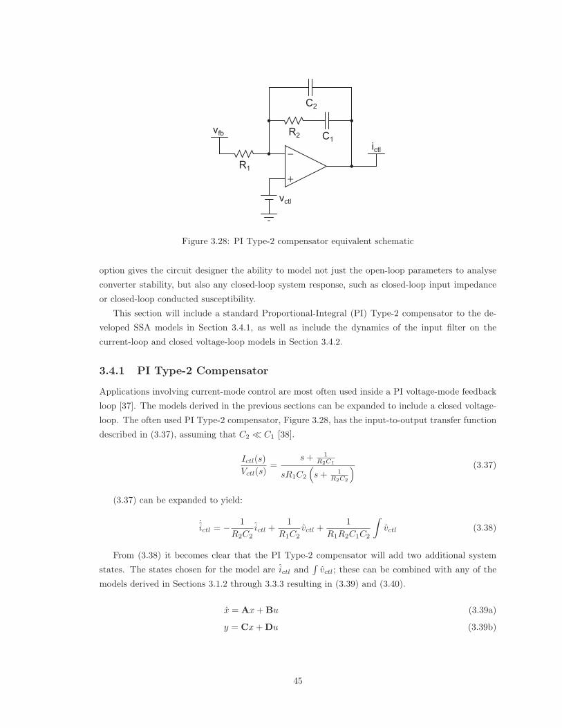
−
+
ictl
R1
R2 C1
C2
vfb
vctl
Figure 3.28: PI Type-2 compensator equivalent schematic
option gives the circuit designer the ability to model not just the open-loop parameters to analyse
converter stability, but also any closed-loop system response, such as closed-loop input impedance
or closed-loop conducted susceptibility.
This section will include a standard Proportional-Integral (PI) Type-2 compensator to the de-
veloped SSA models in Section 3.4.1, as well as include the dynamics of the input filter on the
current-loop and closed voltage-loop models in Section 3.4.2.
3.4.1 PI Type-2 Compensator
Applications involving current-mode control are most often used inside a PI voltage-mode feedback
loop [37]. The models derived in the previous sections can be expanded to include a closed voltage-
loop. The often used PI Type-2 compensator, Figure 3.28, has the input-to-output transfer function
described in (3.37), assuming that C2 � C1 [38].
Ictl(s)
Vctl(s)=
s+ 1R2C1
sR1C2
(s+ 1
R2C2
) (3.37)
(3.37) can be expanded to yield:
˙ictl = − 1
R2C2ictl +
1
R1C2vctl +
1
R1R2C1C2
∫vctl (3.38)
From (3.38) it becomes clear that the PI Type-2 compensator will add two additional system
states. The states chosen for the model are ictl and∫vctl; these can be combined with any of the
models derived in Sections 3.1.2 through 3.3.3 resulting in (3.39) and (3.40).
x = Ax+Bu (3.39a)
y = Cx+Du (3.39b)
45
x =
⎡⎢⎢⎢⎢⎢⎢⎢⎣
iL
vC
d
ictl∫vctl
⎤⎥⎥⎥⎥⎥⎥⎥⎦, y =
[vout
iin
], u =
⎡⎢⎢⎣vd
vctl
io
⎤⎥⎥⎦ (3.39c)
A =
⎡⎢⎢⎢⎢⎢⎢⎢⎣
a1,1 a1,2 a1,3 b1,2 0
a2,1 a2,2 a2,3 b2,2 0
a3,1 a3,2 a3,3 b3,2 0
0 0 0 − 1R2C2
1R1R2C1C2
0 0 0 0 0
⎤⎥⎥⎥⎥⎥⎥⎥⎦
(3.40a)
B =
⎡⎢⎢⎢⎢⎢⎢⎢⎣
b1,1 0 b1,3
b2,1 0 b2,3
b3,1 0 b3,3
0 1R1C2
0
0 1 0
⎤⎥⎥⎥⎥⎥⎥⎥⎦
(3.40b)
C =
[c1,1 c1,2 c1,3 0 0
c2,1 c2,2 c2,3 0 0
](3.40c)
In order to model closed-loop parameters, the A matrix in (3.38) must be replaced by:
A−BK (3.41)
with the K matrix in (3.41) defined by (3.42).
K =
⎡⎢⎢⎣
0 0 0 0 0
c1,1 c1,2 c1,3 0 0
0 0 0 0 0
⎤⎥⎥⎦ (3.42)
From the state equations presented in (3.39), (3.40), (3.41) and (3.42), parameters such as loop
response to determine stability, and closed-loop input impedance, closed-loop conducted suscepti-
bility, as well as closed-loop output impedance, can be determined with ease following the same
procedures followed in Sections 3.2.1 through 3.2.3. The circuit parameters of the Buck converter
analysed in Section 3.2.1, with the addition of a PI Type-2 compensator having a designed crossover
frequency of fc = 5kHz, are plotted in Figures 3.29 through 3.32. These figures illustrate the
versatility of the presented modelling solution.
The derived models not only allow for an outer PI Type-2 voltage-loop to be described, but a
PI Type-3 compensator can also be added to the derived models by following similar steps as those
followed to derive (3.39) through (3.42).
46
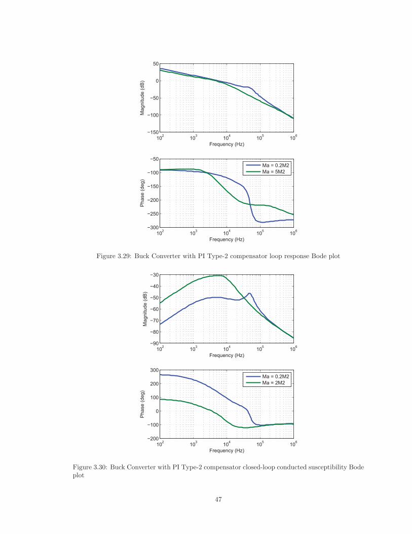
102 103 104 105 106−150
−100
−50
0
50
Mag
nitu
de (d
B)
Frequency (Hz)
102 103 104 105 106−300
−250
−200
−150
−100
−50
Pha
se (d
eg)
Frequency (Hz)
Ma = 0.2M2Ma = 5M2
Figure 3.29: Buck Converter with PI Type-2 compensator loop response Bode plot
102 103 104 105 106−90
−80
−70
−60
−50
−40
−30
Mag
nitu
de (d
B)
Frequency (Hz)
102 103 104 105 106−200
−100
0
100
200
300
Pha
se (d
eg)
Frequency (Hz)
Ma = 0.2M2Ma = 2M2
Figure 3.30: Buck Converter with PI Type-2 compensator closed-loop conducted susceptibility Bodeplot
47
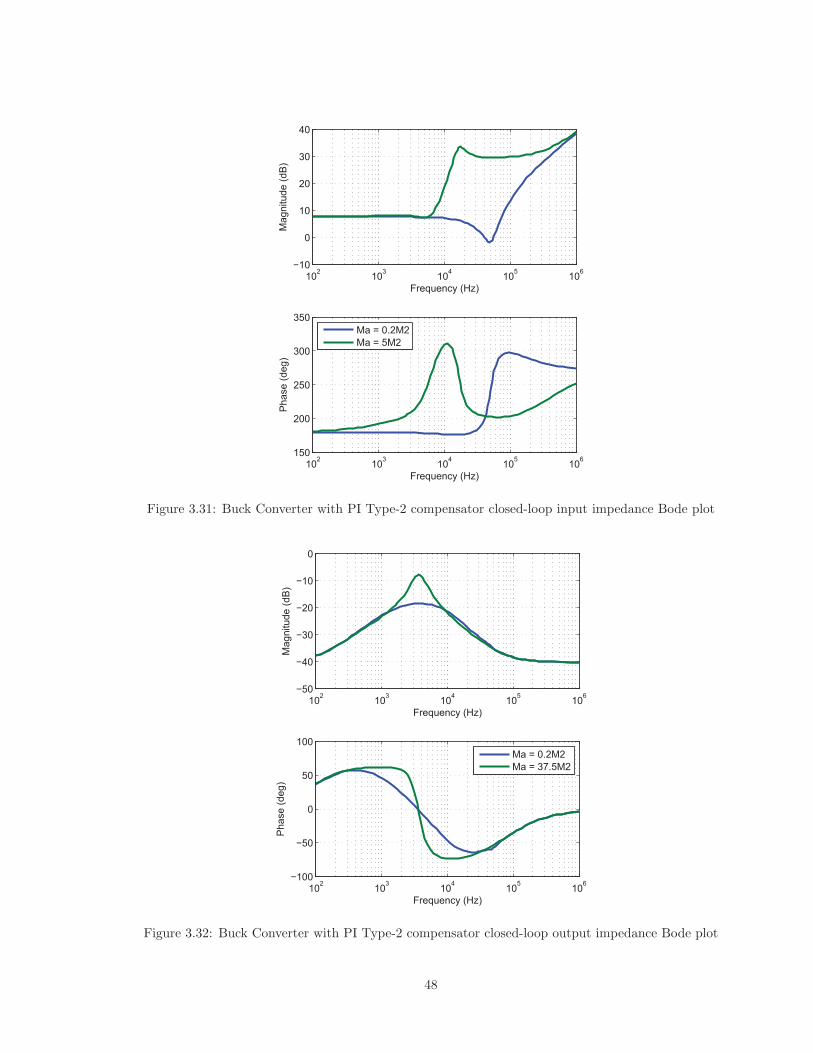
102 103 104 105 106−10
0
10
20
30
40
Mag
nitu
de (d
B)
Frequency (Hz)
102 103 104 105 106150
200
250
300
350
Pha
se (d
eg)
Frequency (Hz)
Ma = 0.2M2Ma = 5M2
Figure 3.31: Buck Converter with PI Type-2 compensator closed-loop input impedance Bode plot
102 103 104 105 106−50
−40
−30
−20
−10
0
Mag
nitu
de (d
B)
Frequency (Hz)
102 103 104 105 106−100
−50
0
50
100
Pha
se (d
eg)
Frequency (Hz)
Ma = 0.2M2Ma = 37.5M2
Figure 3.32: Buck Converter with PI Type-2 compensator closed-loop output impedance Bode plot
48
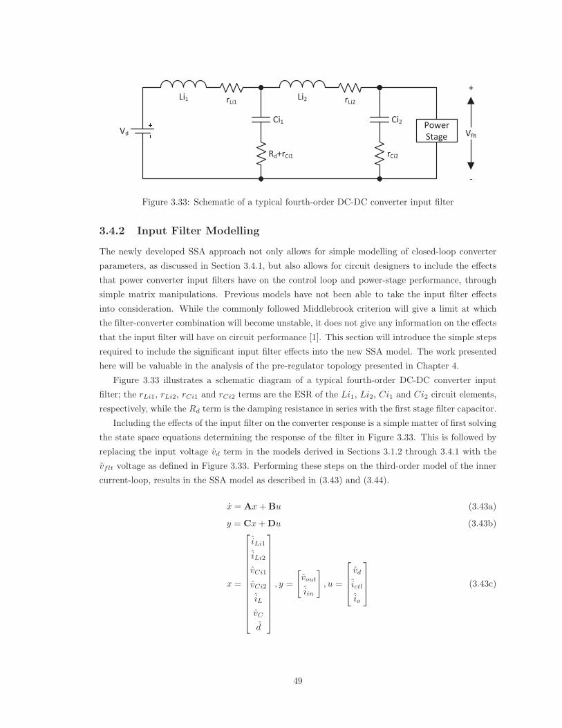
Figure 3.33: Schematic of a typical fourth-order DC-DC converter input filter
3.4.2 Input Filter Modelling
The newly developed SSA approach not only allows for simple modelling of closed-loop converter
parameters, as discussed in Section 3.4.1, but also allows for circuit designers to include the effects
that power converter input filters have on the control loop and power-stage performance, through
simple matrix manipulations. Previous models have not been able to take the input filter effects
into consideration. While the commonly followed Middlebrook criterion will give a limit at which
the filter-converter combination will become unstable, it does not give any information on the effects
that the input filter will have on circuit performance [1]. This section will introduce the simple steps
required to include the significant input filter effects into the new SSA model. The work presented
here will be valuable in the analysis of the pre-regulator topology presented in Chapter 4.
Figure 3.33 illustrates a schematic diagram of a typical fourth-order DC-DC converter input
filter; the rLi1, rLi2, rCi1 and rCi2 terms are the ESR of the Li1, Li2, Ci1 and Ci2 circuit elements,
respectively, while the Rd term is the damping resistance in series with the first stage filter capacitor.
Including the effects of the input filter on the converter response is a simple matter of first solving
the state space equations determining the response of the filter in Figure 3.33. This is followed by
replacing the input voltage vd term in the models derived in Sections 3.1.2 through 3.4.1 with the
vflt voltage as defined in Figure 3.33. Performing these steps on the third-order model of the inner
current-loop, results in the SSA model as described in (3.43) and (3.44).
x = Ax+Bu (3.43a)
y = Cx+Du (3.43b)
x =
⎡⎢⎢⎢⎢⎢⎢⎢⎢⎢⎢⎢⎢⎣
iLi1
iLi2
vCi1
vCi2
iL
vC
d
⎤⎥⎥⎥⎥⎥⎥⎥⎥⎥⎥⎥⎥⎦, y =
[vout
iin
], u =
⎡⎢⎢⎣vd
ictl
io
⎤⎥⎥⎦ (3.43c)
49
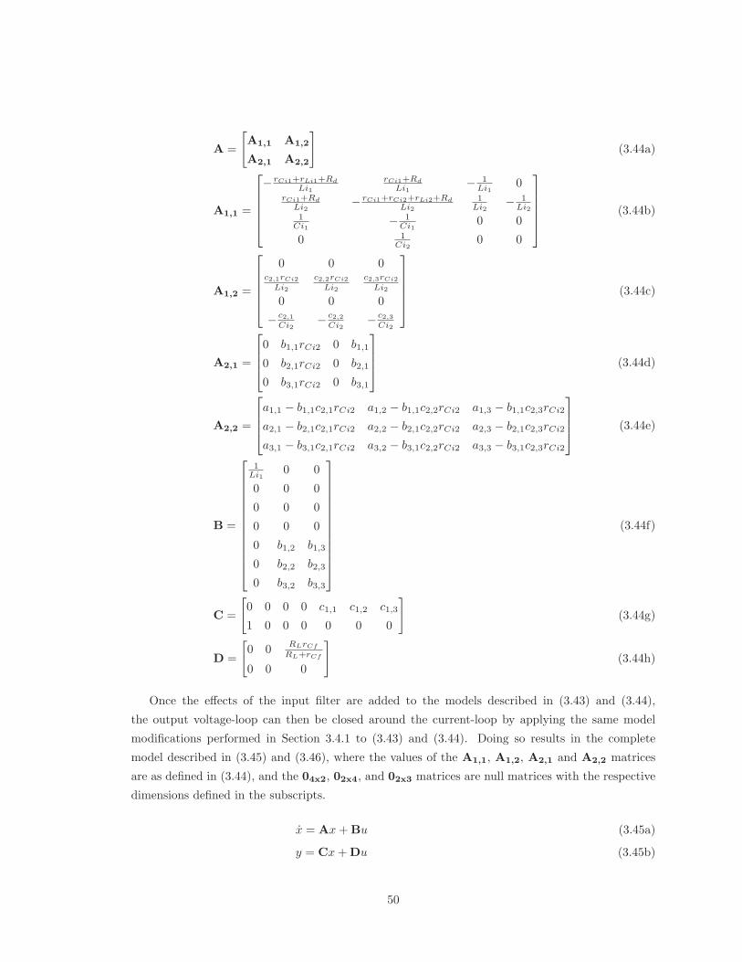
A =
[A1,1 A1,2
A2,1 A2,2
](3.44a)
A1,1 =
⎡⎢⎢⎢⎢⎣− rCi1+rLi1+Rd
Li1rCi1+Rd
Li1− 1
Li10
rCi1+Rd
Li2− rCi1+rCi2+rLi2+Rd
Li21
Li2− 1
Li21
Ci1− 1
Ci10 0
0 1Ci2
0 0
⎤⎥⎥⎥⎥⎦ (3.44b)
A1,2 =
⎡⎢⎢⎢⎢⎣
0 0 0c2,1rCi2
Li2
c2,2rCi2
Li2
c2,3rCi2
Li2
0 0 0
− c2,1Ci2
− c2,2Ci2
− c2,3Ci2
⎤⎥⎥⎥⎥⎦ (3.44c)
A2,1 =
⎡⎢⎢⎣0 b1,1rCi2 0 b1,1
0 b2,1rCi2 0 b2,1
0 b3,1rCi2 0 b3,1
⎤⎥⎥⎦ (3.44d)
A2,2 =
⎡⎢⎢⎣a1,1 − b1,1c2,1rCi2 a1,2 − b1,1c2,2rCi2 a1,3 − b1,1c2,3rCi2
a2,1 − b2,1c2,1rCi2 a2,2 − b2,1c2,2rCi2 a2,3 − b2,1c2,3rCi2
a3,1 − b3,1c2,1rCi2 a3,2 − b3,1c2,2rCi2 a3,3 − b3,1c2,3rCi2
⎤⎥⎥⎦ (3.44e)
B =
⎡⎢⎢⎢⎢⎢⎢⎢⎢⎢⎢⎢⎢⎣
1Li1
0 0
0 0 0
0 0 0
0 0 0
0 b1,2 b1,3
0 b2,2 b2,3
0 b3,2 b3,3
⎤⎥⎥⎥⎥⎥⎥⎥⎥⎥⎥⎥⎥⎦
(3.44f)
C =
[0 0 0 0 c1,1 c1,2 c1,3
1 0 0 0 0 0 0
](3.44g)
D =
[0 0
RLrCf
RL+rCf
0 0 0
](3.44h)
Once the effects of the input filter are added to the models described in (3.43) and (3.44),
the output voltage-loop can then be closed around the current-loop by applying the same model
modifications performed in Section 3.4.1 to (3.43) and (3.44). Doing so results in the complete
model described in (3.45) and (3.46), where the values of the A1,1, A1,2, A2,1 and A2,2 matrices
are as defined in (3.44), and the 04x2, 02x4, and 02x3 matrices are null matrices with the respective
dimensions defined in the subscripts.
x = Ax+Bu (3.45a)
y = Cx+Du (3.45b)
50
x =
⎡⎢⎢⎢⎢⎢⎢⎢⎢⎢⎢⎢⎢⎢⎢⎢⎢⎢⎣
iLi1
iLi2
vCi1
vCi2
iL
vC
d
ictl∫vctl
⎤⎥⎥⎥⎥⎥⎥⎥⎥⎥⎥⎥⎥⎥⎥⎥⎥⎥⎦
, y =
[vout
iin
], u =
⎡⎢⎢⎣vd
vctl
io
⎤⎥⎥⎦ (3.45c)
A =
⎡⎢⎢⎣A1,1 A1,2 04x2
A2,1 A2,2 A2,3
02x4 02x3 A3,3
⎤⎥⎥⎦ (3.46a)
A2,3 =
⎡⎢⎢⎣b1,2 0
b2,2 0
b3,2 0
⎤⎥⎥⎦ (3.46b)
A3,3 =
[− 1
R2C2
1R1R2C1C2
0 0
](3.46c)
B =
⎡⎢⎢⎢⎢⎢⎢⎢⎢⎢⎢⎢⎢⎢⎢⎢⎢⎢⎣
1Li1
0 0
0 0 0
0 0 0
0 0 0
0 0 b1,3
0 0 b2,3
0 0 b3,3
0 1R1C2
0
0 1 0
⎤⎥⎥⎥⎥⎥⎥⎥⎥⎥⎥⎥⎥⎥⎥⎥⎥⎥⎦
(3.46d)
C =
[0 0 0 0 c1,1 c1,2 c1,3 0 0
1 0 0 0 0 0 0 0 0
](3.46e)
D =
[0 0
RLrCf
RL+rCf
0 0 0
](3.46f)
In [39], an attempt is made to model the effects the input filter has on a PCM controlled DC-
DC converter. This work retained the classical transfer function models of the current-loop and
added a state space representation of the input filter to complete the model. In contrast, the model
proposed in this chapter allows for more accurate modelling of the current-loop, and in turn, the
entire converter [39].
51
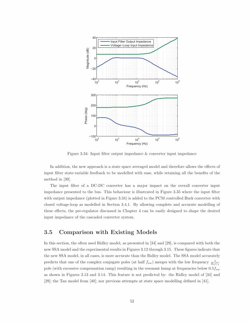
102 103 104 105 106−40
−20
0
20
40
Mag
nitu
de (d
B)
Frequency (Hz)
Input Filter Output ImpedanceVoltage−Loop Input Impedance
102 103 104 105 106−100
0
100
200
300
Pha
se (d
eg)
Frequency (Hz)
Figure 3.34: Input filter output impedance & converter input impedance
In addition, the new approach is a state space averaged model and therefore allows the effects of
input filter state-variable feedback to be modelled with ease, while retaining all the benefits of the
method in [39].
The input filter of a DC-DC converter has a major impact on the overall converter input
impedance presented to the bus. This behaviour is illustrated in Figure 3.35 where the input filter
with output impedance (plotted in Figure 3.34) is added to the PCM controlled Buck converter with
closed voltage-loop as modelled in Section 3.4.1. By allowing complete and accurate modelling of
these effects, the pre-regulator discussed in Chapter 4 can be easily designed to shape the desired
input impedance of the cascaded converter system.
3.5 Comparison with Existing Models
In this section, the often used Ridley model, as presented in [34] and [29], is compared with both the
new SSA model and the experimental results in Figures 3.12 through 3.15. These figures indicate that
the new SSA model, in all cases, is more accurate than the Ridley model. The SSA model accurately
predicts that one of the complex conjugate poles (at half fsw) merges with the low frequency 1RLCf
pole (with excessive compensation ramp) resulting in the resonant hump at frequencies below 0.5fsw
as shown in Figures 3.13 and 3.14. This feature is not predicted by: the Ridley model of [34] and
[29]; the Tan model from [40]; nor previous attempts at state space modelling defined in [41].
52
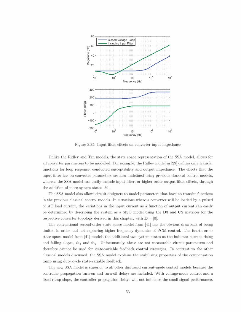
102 103 104 105 1060
20
40
60
80
Mag
nitu
de (d
B)
Frequency (Hz)
Closed Voltage−LoopIncluding Input Filter
102 103 104 105 106−200
−100
0
100
200
300
Pha
se (d
eg)
Frequency (Hz)
Figure 3.35: Input filter effects on converter input impedance
Unlike the Ridley and Tan models, the state space representation of the SSA model, allows for
all converter parameters to be modelled. For example, the Ridley model in [29] defines only transfer
functions for loop response, conducted susceptibility and output impedance. The effects that the
input filter has on converter parameters are also undefined using previous classical control models,
whereas the SSA model can easily include input filter, or higher order output filter effects, through
the addition of more system states [39].
The SSA model also allows circuit designers to model parameters that have no transfer functions
in the previous classical control models. In situations where a converter will be loaded by a pulsed
or AC load current, the variations in the input current as a function of output current can easily
be determined by describing the system as a SISO model using the B3 and C2 matrices for the
respective converter topology derived in this chapter, with D = [0].
The conventional second-order state space model from [41] has the obvious drawback of being
limited in order and not capturing higher frequency dynamics of PCM control. The fourth-order
state space model from [41] models the additional two system states as the inductor current rising
and falling slopes, m1 and m2. Unfortunately, these are not measurable circuit parameters and
therefore cannot be used for state-variable feedback control strategies. In contrast to the other
classical models discussed, the SSA model explains the stabilising properties of the compensation
ramp using duty cycle state-variable feedback.
The new SSA model is superior to all other discussed current-mode control models because the
controller propagation turn-on and turn-off delays are included. With voltage-mode control and a
fixed ramp slope, the controller propagation delays will not influence the small-signal performance.
53
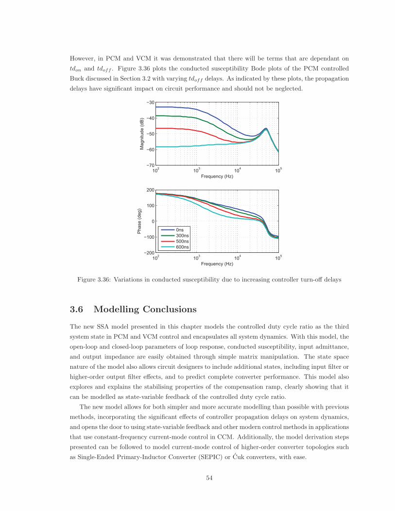
However, in PCM and VCM it was demonstrated that there will be terms that are dependant on
tdon and tdoff . Figure 3.36 plots the conducted susceptibility Bode plots of the PCM controlled
Buck discussed in Section 3.2 with varying tdoff delays. As indicated by these plots, the propagation
delays have significant impact on circuit performance and should not be neglected.
102 103 104 105−70
−60
−50
−40
−30
Mag
nitu
de (d
B)
Frequency (Hz)
102 103 104 105−200
−100
0
100
200
Pha
se (d
eg)
Frequency (Hz)
0ns300ns500ns600ns
Figure 3.36: Variations in conducted susceptibility due to increasing controller turn-off delays
3.6 Modelling Conclusions
The new SSA model presented in this chapter models the controlled duty cycle ratio as the third
system state in PCM and VCM control and encapsulates all system dynamics. With this model, the
open-loop and closed-loop parameters of loop response, conducted susceptibility, input admittance,
and output impedance are easily obtained through simple matrix manipulation. The state space
nature of the model also allows circuit designers to include additional states, including input filter or
higher-order output filter effects, and to predict complete converter performance. This model also
explores and explains the stabilising properties of the compensation ramp, clearly showing that it
can be modelled as state-variable feedback of the controlled duty cycle ratio.
The new model allows for both simpler and more accurate modelling than possible with previous
methods, incorporating the significant effects of controller propagation delays on system dynamics,
and opens the door to using state-variable feedback and other modern control methods in applications
that use constant-frequency current-mode control in CCM. Additionally, the model derivation steps
presented can be followed to model current-mode control of higher-order converter topologies such
as Single-Ended Primary-Inductor Converter (SEPIC) or Cuk converters, with ease.
54
Chapter 4
An Input Impedance Shaping
Pre-Regulator
4.1 Proposed Pre-Regulator Topology
While the pre-regulator general topology introduced in Section 2.2 will allow for the desired input
impedance shaping of the power electronic CPLs, inherent to the design is the significant downside
of requiring an analogue multiplier block. Disadvantages of linear multiplier circuits lies in their
inherent sensitivity to noise and limited operating ranges [42]. The alternative of using digital
multipliers adds to overall pre-regulator costs, forcing the use of costly digital control ICs with
significantly slower switching frequencies than current analogue counterparts. However, the most
significant disadvantage of the linear multiplier is that the control circuitry requires another IC
in addition to the PWM controller, increasing costs and converter PCB real-estate or requiring
specialised control ICs with the multipliers on-die.
Since the desired pre-regulator will operate from a DC bus, the input bus voltage will not change
significantly. In addition, the input impedance needs only to be shaped to match small-signal
variations. The linear multiplier from Figure 2.4 can therefore be replaced with an input bus voltage
feed-forward gain, as shown in Figure 4.1.
The voltage feed-forward gain term will therefore modulate the peak (or valley) input inductor
current as a function of small-signal input bus variation. The modulated desired input current is
then summed with the output of the error-amplifier (which must maintain a low bandwidth loop
response). At frequencies below the error amplifier loop crossover frequency, the input impedance
will be negative. At frequencies below the voltage-loop compensation bandwidth, the dominant
signal modulating the desired inductor current will be from the error-amplifier feedback, as shown
in Figure 4.2. This will result in the output being regulated to a constant DC-link voltage which
the load converter (or constant input power motor driver, etc.) will use as input bus voltage.
55
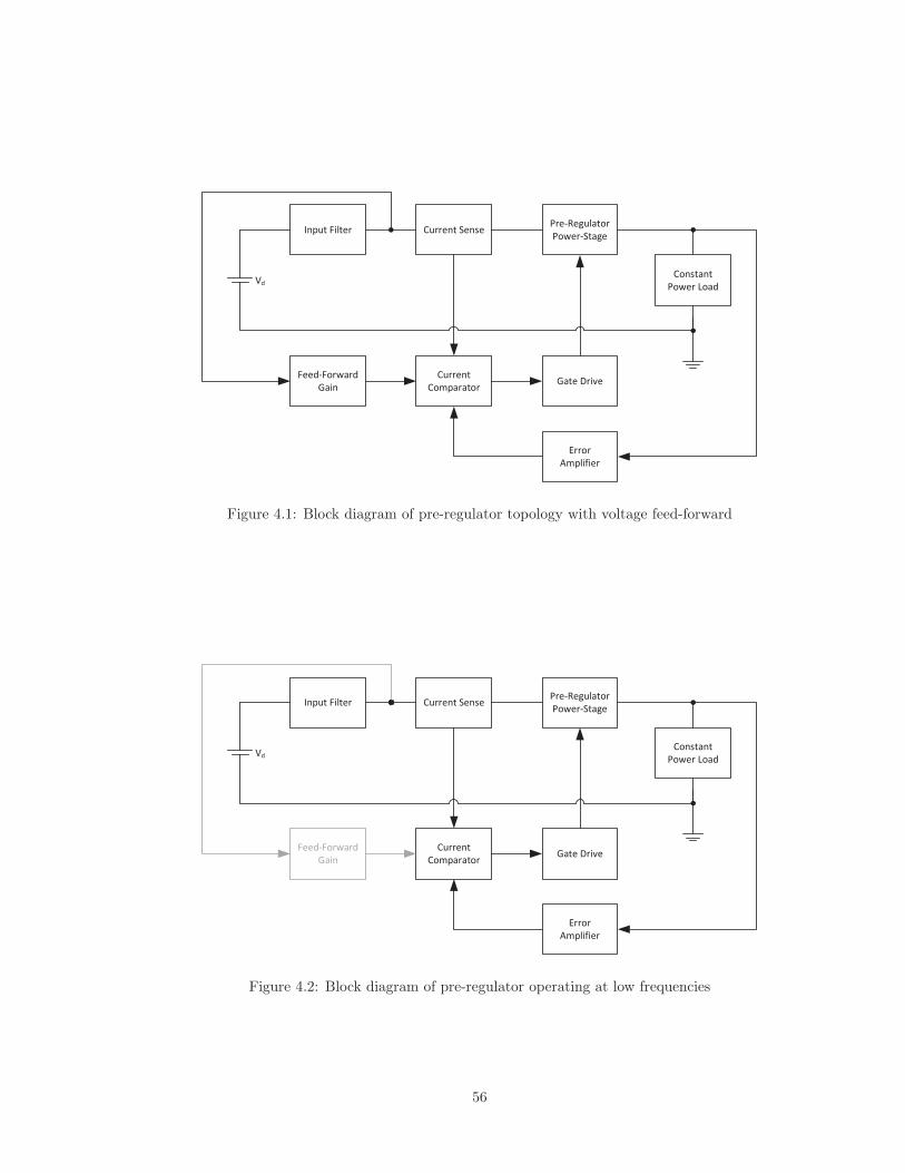
Figure 4.1: Block diagram of pre-regulator topology with voltage feed-forward
Figure 4.2: Block diagram of pre-regulator operating at low frequencies
56
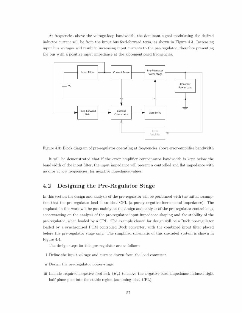
At frequencies above the voltage-loop bandwidth, the dominant signal modulating the desired
inductor current will be from the input bus feed-forward term, as shown in Figure 4.3. Increasing
input bus voltages will result in increasing input currents to the pre-regulator, therefore presenting
the bus with a positive input impedance at the aforementioned frequencies.
Figure 4.3: Block diagram of pre-regulator operating at frequencies above error-amplifier bandwidth
It will be demonstrated that if the error amplifier compensator bandwidth is kept below the
bandwidth of the input filter, the input impedance will present a controlled and flat impedance with
no dips at low frequencies, for negative impedance values.
4.2 Designing the Pre-Regulator Stage
In this section the design and analysis of the pre-regulator will be performed with the initial assump-
tion that the pre-regulator load is an ideal CPL (a purely negative incremental impedance). The
emphasis in this work will be put mainly on the design and analysis of the pre-regulator control loop,
concentrating on the analysis of the pre-regulator input impedance shaping and the stability of the
pre-regulator, when loaded by a CPL. The example chosen for design will be a Buck pre-regulator
loaded by a synchronised PCM controlled Buck converter, with the combined input filter placed
before the pre-regulator stage only. The simplified schematic of this cascaded system is shown in
Figure 4.4.
The design steps for this pre-regulator are as follows:
i Define the input voltage and current drawn from the load converter.
ii Design the pre-regulator power-stage.
iii Include required negative feedback (Kp) to move the negative load impedance induced right
half-plane pole into the stable region (assuming ideal CPL).
57
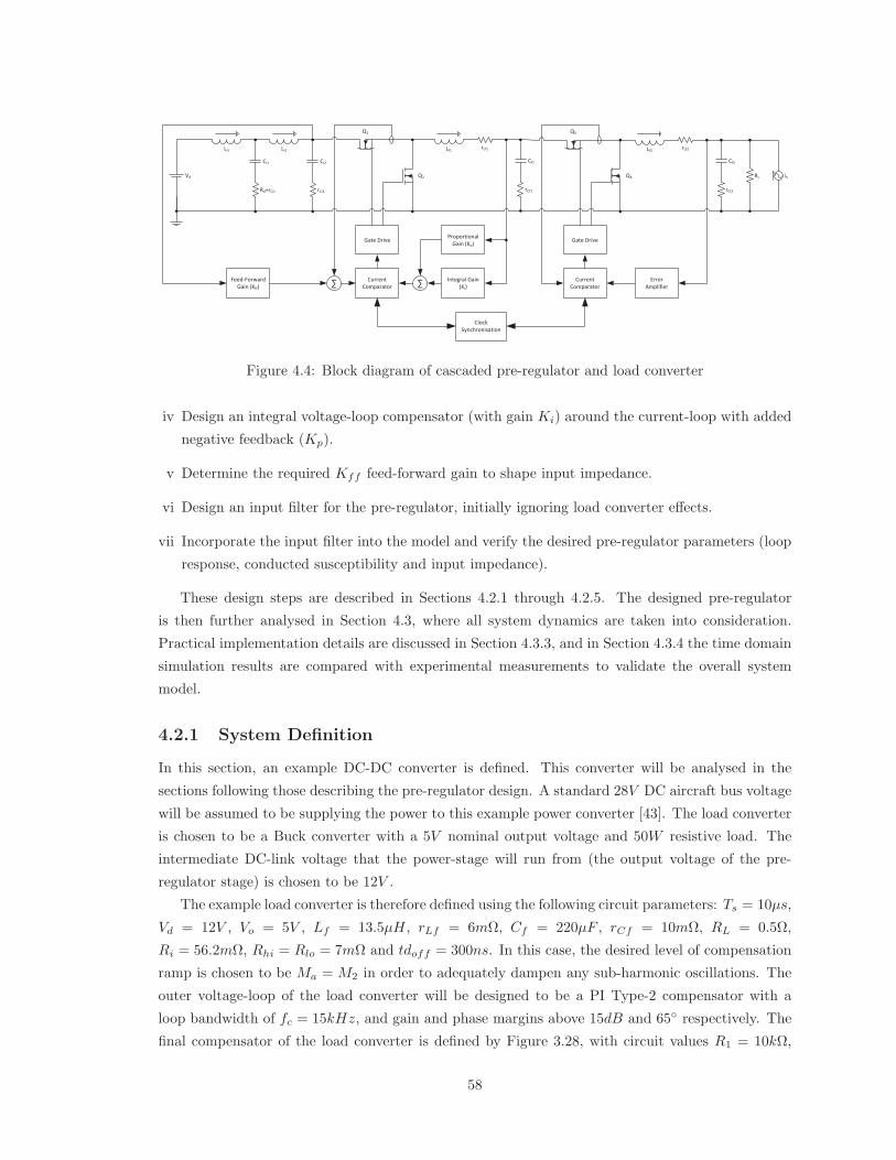
Figure 4.4: Block diagram of cascaded pre-regulator and load converter
iv Design an integral voltage-loop compensator (with gain Ki) around the current-loop with added
negative feedback (Kp).
v Determine the required Kff feed-forward gain to shape input impedance.
vi Design an input filter for the pre-regulator, initially ignoring load converter effects.
vii Incorporate the input filter into the model and verify the desired pre-regulator parameters (loop
response, conducted susceptibility and input impedance).
These design steps are described in Sections 4.2.1 through 4.2.5. The designed pre-regulator
is then further analysed in Section 4.3, where all system dynamics are taken into consideration.
Practical implementation details are discussed in Section 4.3.3, and in Section 4.3.4 the time domain
simulation results are compared with experimental measurements to validate the overall system
model.
4.2.1 System Definition
In this section, an example DC-DC converter is defined. This converter will be analysed in the
sections following those describing the pre-regulator design. A standard 28V DC aircraft bus voltage
will be assumed to be supplying the power to this example power converter [43]. The load converter
is chosen to be a Buck converter with a 5V nominal output voltage and 50W resistive load. The
intermediate DC-link voltage that the power-stage will run from (the output voltage of the pre-
regulator stage) is chosen to be 12V .
The example load converter is therefore defined using the following circuit parameters: Ts = 10μs,
Vd = 12V , Vo = 5V , Lf = 13.5μH, rLf = 6mΩ, Cf = 220μF , rCf = 10mΩ, RL = 0.5Ω,
Ri = 56.2mΩ, Rhi = Rlo = 7mΩ and tdoff = 300ns. In this case, the desired level of compensation
ramp is chosen to be Ma = M2 in order to adequately dampen any sub-harmonic oscillations. The
outer voltage-loop of the load converter will be designed to be a PI Type-2 compensator with a
loop bandwidth of fc = 15kHz, and gain and phase margins above 15dB and 65◦ respectively. The
final compensator of the load converter is defined by Figure 3.28, with circuit values R1 = 10kΩ,
58
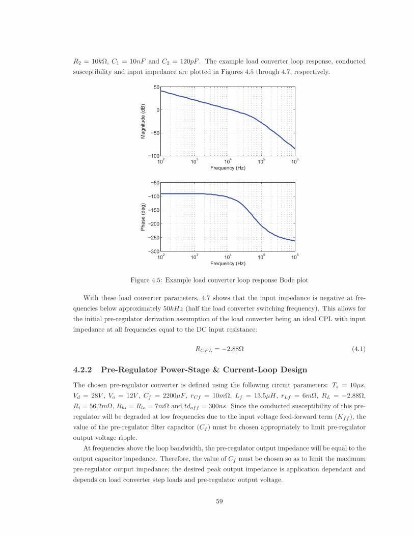
R2 = 10kΩ, C1 = 10nF and C2 = 120pF . The example load converter loop response, conducted
susceptibility and input impedance are plotted in Figures 4.5 through 4.7, respectively.
102 103 104 105 106−100
−50
0
50
Mag
nitu
de (d
B)
Frequency (Hz)
102 103 104 105 106−300
−250
−200
−150
−100
−50
Pha
se (d
eg)
Frequency (Hz)
Figure 4.5: Example load converter loop response Bode plot
With these load converter parameters, 4.7 shows that the input impedance is negative at fre-
quencies below approximately 50kHz (half the load converter switching frequency). This allows for
the initial pre-regulator derivation assumption of the load converter being an ideal CPL with input
impedance at all frequencies equal to the DC input resistance:
RCPL = −2.88Ω (4.1)
4.2.2 Pre-Regulator Power-Stage & Current-Loop Design
The chosen pre-regulator converter is defined using the following circuit parameters: Ts = 10μs,
Vd = 28V , Vo = 12V , Cf = 2200μF , rCf = 10mΩ, Lf = 13.5μH, rLf = 6mΩ, RL = −2.88Ω,
Ri = 56.2mΩ, Rhi = Rlo = 7mΩ and tdoff = 300ns. Since the conducted susceptibility of this pre-
regulator will be degraded at low frequencies due to the input voltage feed-forward term (Kff ), the
value of the pre-regulator filter capacitor (Cf ) must be chosen appropriately to limit pre-regulator
output voltage ripple.
At frequencies above the loop bandwidth, the pre-regulator output impedance will be equal to the
output capacitor impedance. Therefore, the value of Cf must be chosen so as to limit the maximum
pre-regulator output impedance; the desired peak output impedance is application dependant and
depends on load converter step loads and pre-regulator output voltage.
59
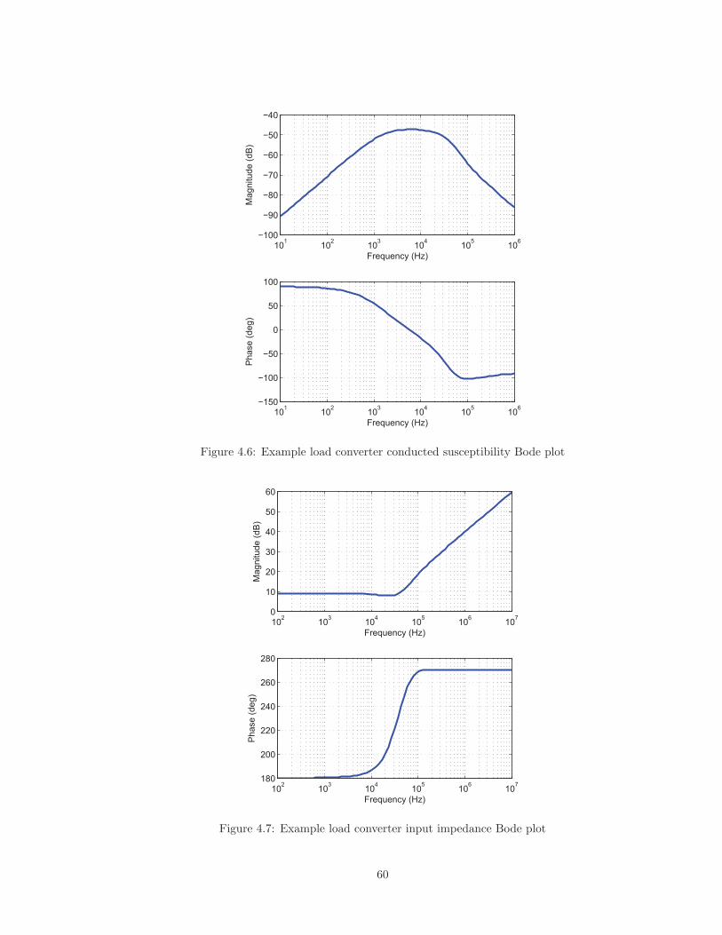
101 102 103 104 105 106−100
−90
−80
−70
−60
−50
−40
Mag
nitu
de (d
B)
Frequency (Hz)
101 102 103 104 105 106−150
−100
−50
0
50
100
Pha
se (d
eg)
Frequency (Hz)
Figure 4.6: Example load converter conducted susceptibility Bode plot
102 103 104 105 106 1070
10
20
30
40
50
60
Mag
nitu
de (d
B)
Frequency (Hz)
102 103 104 105 106 107180
200
220
240
260
280
Pha
se (d
eg)
Frequency (Hz)
Figure 4.7: Example load converter input impedance Bode plot
60

The higher the pre-regulator output voltages, the higher the resulting equivalent input impedance
of the load converter, therefore reducing the need for larger Cf values. This inversely proportional
nature between the DC-link voltage and the minimum required pre-regulator filter capacitance, is
best described by a Boost pre-regulator topology.
Given this final power-stage design, the initial current-loop root locus plot, in absence of any
compensation ramp, is illustrated in Figure 4.8. The negative load impedance destabilises the pre-
regulator; this is evident from the low frequency pole in Figure 4.8 residing in the right half-plane.
−7 −6 −5 −4 −3 −2 −1 0 1 2
x 104
−1
−0.5
0
0.5
1x 10
6Root Locus
Real Axis (seconds−1)
Imag
inar
y A
xis
(sec
onds
−1)
−500 0 500−1000
−500
0
500
1000
Expanded View
Real Axis (seconds−1)
Imag
inar
y A
xis
(sec
onds
−1)
Figure 4.8: Example pre-regulator initial loop response root locus plot
However, also indicated by Figure 4.8 is with increasing output voltage negative-feedback, the
unstable pole can be brought into the left half-plane. This has the disadvantage of pushing the
complex-conjugate poles, at half the switching frequency, closer to the jω axis, resulting in the
degradation of stability margins. Since the model developed in Chapter 3 is a modern state space
model, the poles can be arbitrarily placed where desired. An initial choice for this design is the
frequency above which the input impedance becomes positive. For this example a value of 100Hz has
been selected resulting in the desired position of the output filter low-frequency pole at fp = 100Hz.
In order to move the complex-conjugate poles from half the switching frequency requires feedback
of the inductor current. In order to simplify the feedback control, the complex-conjugate poles will
be kept at half the switching frequency and the control parameters will be defined by the desired
damping factor of the complex-conjugate poles and the position of the output load impedance pole.
61
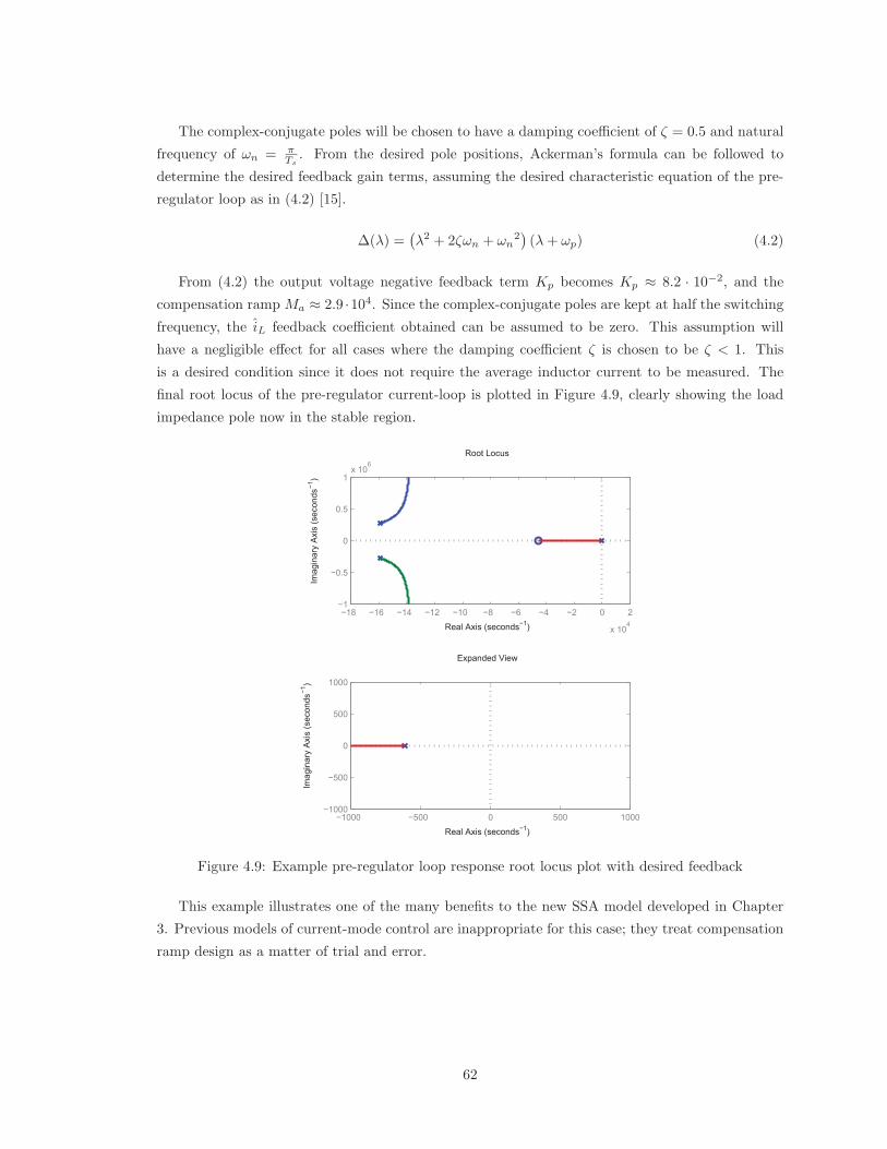
The complex-conjugate poles will be chosen to have a damping coefficient of ζ = 0.5 and natural
frequency of ωn = πTs. From the desired pole positions, Ackerman’s formula can be followed to
determine the desired feedback gain terms, assuming the desired characteristic equation of the pre-
regulator loop as in (4.2) [15].
Δ(λ) =(λ2 + 2ζωn + ωn
2)(λ+ ωp) (4.2)
From (4.2) the output voltage negative feedback term Kp becomes Kp ≈ 8.2 · 10−2, and the
compensation ramp Ma ≈ 2.9 ·104. Since the complex-conjugate poles are kept at half the switching
frequency, the iL feedback coefficient obtained can be assumed to be zero. This assumption will
have a negligible effect for all cases where the damping coefficient ζ is chosen to be ζ < 1. This
is a desired condition since it does not require the average inductor current to be measured. The
final root locus of the pre-regulator current-loop is plotted in Figure 4.9, clearly showing the load
impedance pole now in the stable region.
−18 −16 −14 −12 −10 −8 −6 −4 −2 0 2
x 104
−1
−0.5
0
0.5
1x 10
6Root Locus
Real Axis (seconds−1)
Imag
inar
y A
xis
(sec
onds
−1)
−1000 −500 0 500 1000−1000
−500
0
500
1000
Expanded View
Real Axis (seconds−1)
Imag
inar
y A
xis
(sec
onds
−1)
Figure 4.9: Example pre-regulator loop response root locus plot with desired feedback
This example illustrates one of the many benefits to the new SSA model developed in Chapter
3. Previous models of current-mode control are inappropriate for this case; they treat compensation
ramp design as a matter of trial and error.
62
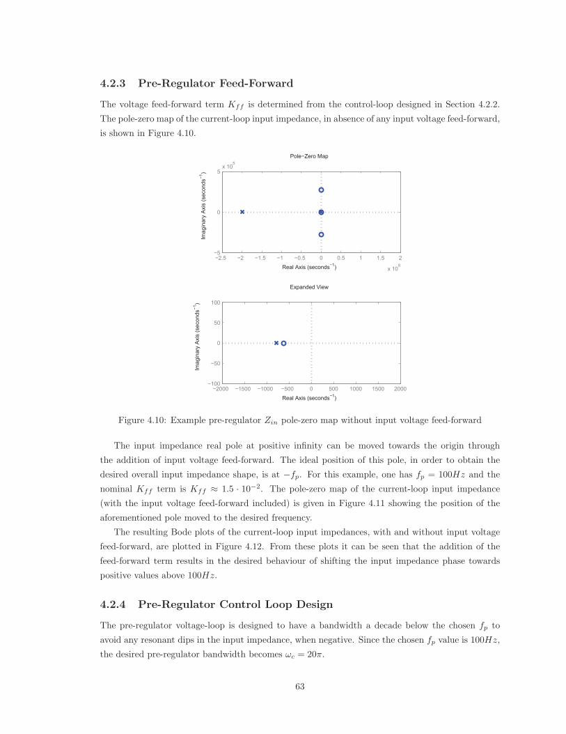
4.2.3 Pre-Regulator Feed-Forward
The voltage feed-forward term Kff is determined from the control-loop designed in Section 4.2.2.
The pole-zero map of the current-loop input impedance, in absence of any input voltage feed-forward,
is shown in Figure 4.10.
−2.5 −2 −1.5 −1 −0.5 0 0.5 1 1.5 2
x 108
−5
0
5x 10
5Pole−Zero Map
Real Axis (seconds−1)
Imag
inar
y A
xis
(sec
onds
−1)
−2000 −1500 −1000 −500 0 500 1000 1500 2000−100
−50
0
50
100
Expanded View
Real Axis (seconds−1)
Imag
inar
y A
xis
(sec
onds
−1)
Figure 4.10: Example pre-regulator Zin pole-zero map without input voltage feed-forward
The input impedance real pole at positive infinity can be moved towards the origin through
the addition of input voltage feed-forward. The ideal position of this pole, in order to obtain the
desired overall input impedance shape, is at −fp. For this example, one has fp = 100Hz and the
nominal Kff term is Kff ≈ 1.5 · 10−2. The pole-zero map of the current-loop input impedance
(with the input voltage feed-forward included) is given in Figure 4.11 showing the position of the
aforementioned pole moved to the desired frequency.
The resulting Bode plots of the current-loop input impedances, with and without input voltage
feed-forward, are plotted in Figure 4.12. From these plots it can be seen that the addition of the
feed-forward term results in the desired behaviour of shifting the input impedance phase towards
positive values above 100Hz.
4.2.4 Pre-Regulator Control Loop Design
The pre-regulator voltage-loop is designed to have a bandwidth a decade below the chosen fp to
avoid any resonant dips in the input impedance, when negative. Since the chosen fp value is 100Hz,
the desired pre-regulator bandwidth becomes ωc = 20π.
63
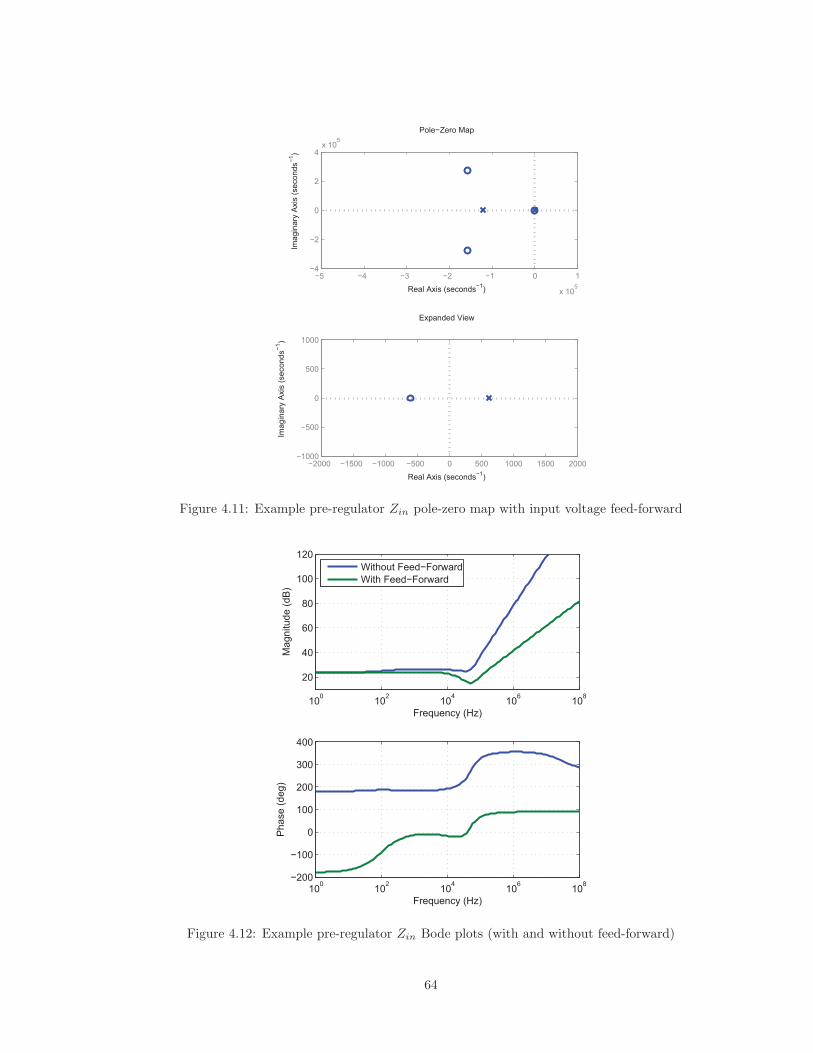
−5 −4 −3 −2 −1 0 1
x 105
−4
−2
0
2
4x 10
5Pole−Zero Map
Real Axis (seconds−1)Im
agin
ary
Axi
s (s
econ
ds−1
)
−2000 −1500 −1000 −500 0 500 1000 1500 2000−1000
−500
0
500
1000
Expanded View
Real Axis (seconds−1)
Imag
inar
y A
xis
(sec
onds
−1)
Figure 4.11: Example pre-regulator Zin pole-zero map with input voltage feed-forward
100 102 104 106 108
20
40
60
80
100
120
Mag
nitu
de (d
B)
Frequency (Hz)
Without Feed−ForwardWith Feed−Forward
100 102 104 106 108−200
−100
0
100
200
300
400
Pha
se (d
eg)
Frequency (Hz)
Figure 4.12: Example pre-regulator Zin Bode plots (with and without feed-forward)
64
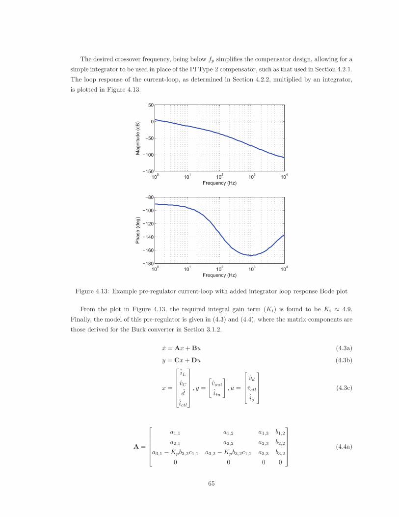
The desired crossover frequency, being below fp simplifies the compensator design, allowing for a
simple integrator to be used in place of the PI Type-2 compensator, such as that used in Section 4.2.1.
The loop response of the current-loop, as determined in Section 4.2.2, multiplied by an integrator,
is plotted in Figure 4.13.
100 101 102 103 104−150
−100
−50
0
50
Mag
nitu
de (d
B)
Frequency (Hz)
100 101 102 103 104−180
−160
−140
−120
−100
−80
Pha
se (d
eg)
Frequency (Hz)
Figure 4.13: Example pre-regulator current-loop with added integrator loop response Bode plot
From the plot in Figure 4.13, the required integral gain term (Ki) is found to be Ki ≈ 4.9.
Finally, the model of this pre-regulator is given in (4.3) and (4.4), where the matrix components are
those derived for the Buck converter in Section 3.1.2.
x = Ax+Bu (4.3a)
y = Cx+Du (4.3b)
x =
⎡⎢⎢⎢⎢⎣iL
vC
d
ictl
⎤⎥⎥⎥⎥⎦ , y =
[vout
iin
], u =
⎡⎢⎢⎣vd
vctl
io
⎤⎥⎥⎦ (4.3c)
A =
⎡⎢⎢⎢⎢⎣
a1,1 a1,2 a1,3 b1,2
a2,1 a2,2 a2,3 b2,2
a3,1 −Kpb3,2c1,1 a3,2 −Kpb3,2c1,2 a3,3 b3,2
0 0 0 0
⎤⎥⎥⎥⎥⎦ (4.4a)
65
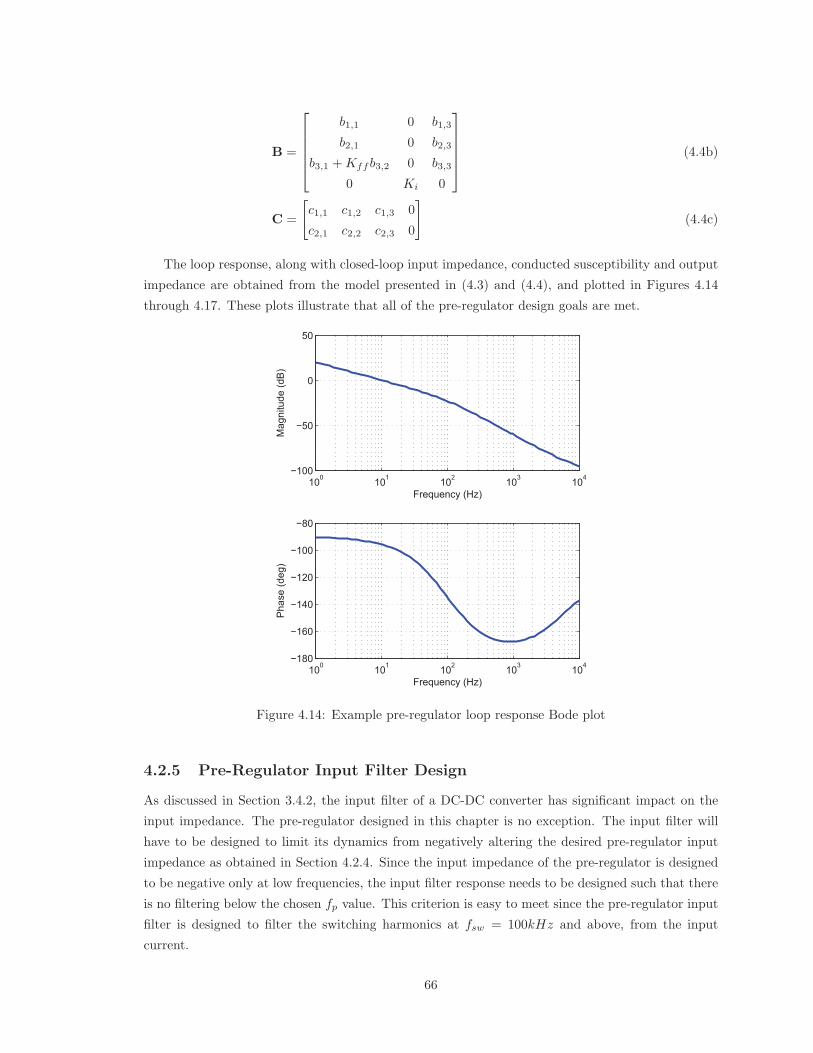
B =
⎡⎢⎢⎢⎢⎣
b1,1 0 b1,3
b2,1 0 b2,3
b3,1 +Kffb3,2 0 b3,3
0 Ki 0
⎤⎥⎥⎥⎥⎦ (4.4b)
C =
[c1,1 c1,2 c1,3 0
c2,1 c2,2 c2,3 0
](4.4c)
The loop response, along with closed-loop input impedance, conducted susceptibility and output
impedance are obtained from the model presented in (4.3) and (4.4), and plotted in Figures 4.14
through 4.17. These plots illustrate that all of the pre-regulator design goals are met.
100 101 102 103 104−100
−50
0
50
Mag
nitu
de (d
B)
Frequency (Hz)
100 101 102 103 104−180
−160
−140
−120
−100
−80
Pha
se (d
eg)
Frequency (Hz)
Figure 4.14: Example pre-regulator loop response Bode plot
4.2.5 Pre-Regulator Input Filter Design
As discussed in Section 3.4.2, the input filter of a DC-DC converter has significant impact on the
input impedance. The pre-regulator designed in this chapter is no exception. The input filter will
have to be designed to limit its dynamics from negatively altering the desired pre-regulator input
impedance as obtained in Section 4.2.4. Since the input impedance of the pre-regulator is designed
to be negative only at low frequencies, the input filter response needs to be designed such that there
is no filtering below the chosen fp value. This criterion is easy to meet since the pre-regulator input
filter is designed to filter the switching harmonics at fsw = 100kHz and above, from the input
current.
66
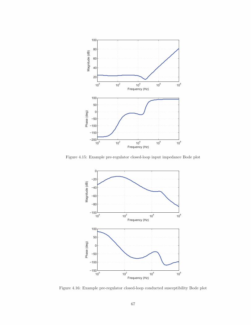
100 102 104 106 108
20
40
60
80
100
Mag
nitu
de (d
B)
Frequency (Hz)
100 102 104 106 108−200
−150
−100
−50
0
50
100
Pha
se (d
eg)
Frequency (Hz)
Figure 4.15: Example pre-regulator closed-loop input impedance Bode plot
100 102 104 106−100
−80
−60
−40
−20
0
Mag
nitu
de (d
B)
Frequency (Hz)
100 102 104 106−150
−100
−50
0
50
100
Pha
se (d
eg)
Frequency (Hz)
Figure 4.16: Example pre-regulator closed-loop conducted susceptibility Bode plot
67
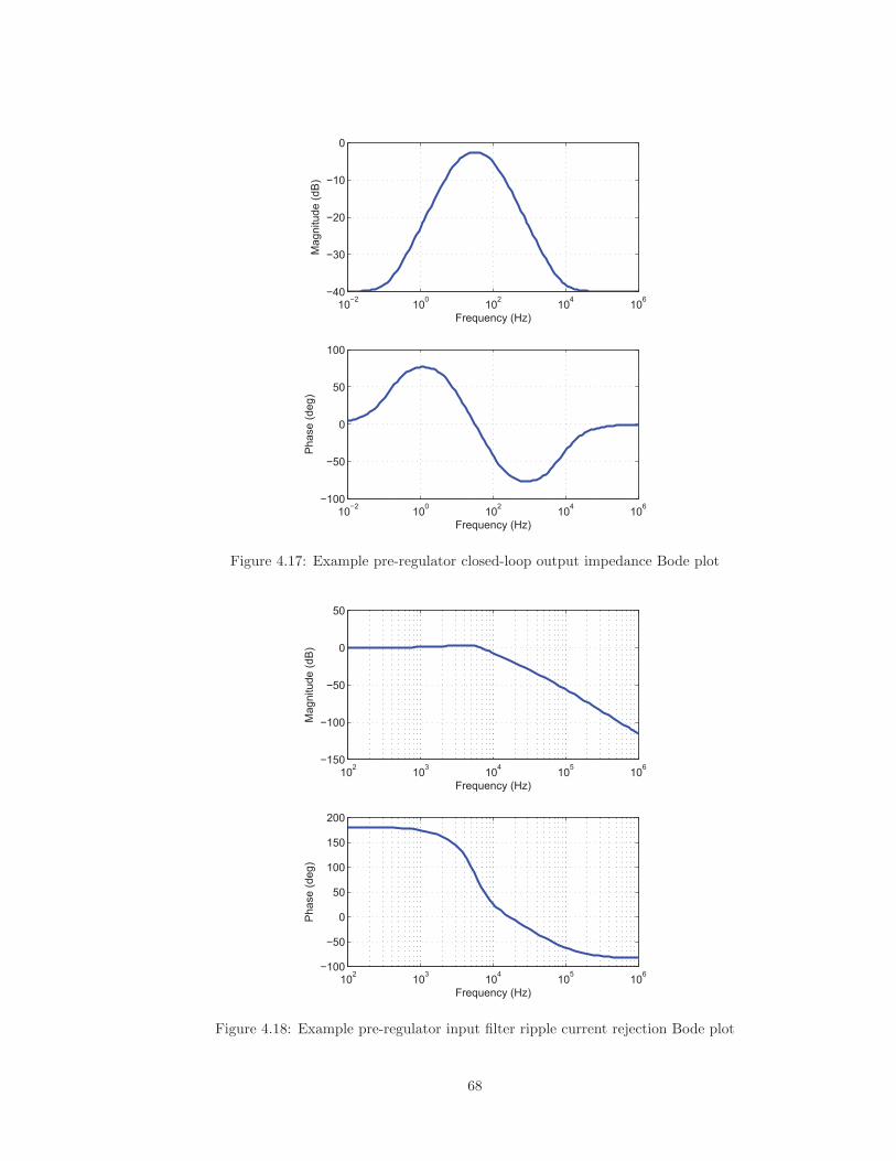
10−2 100 102 104 106−40
−30
−20
−10
0
Mag
nitu
de (d
B)
Frequency (Hz)
10−2 100 102 104 106−100
−50
0
50
100
Pha
se (d
eg)
Frequency (Hz)
Figure 4.17: Example pre-regulator closed-loop output impedance Bode plot
102 103 104 105 106−150
−100
−50
0
50
Mag
nitu
de (d
B)
Frequency (Hz)
102 103 104 105 106−100
−50
0
50
100
150
200
Pha
se (d
eg)
Frequency (Hz)
Figure 4.18: Example pre-regulator input filter ripple current rejection Bode plot
68
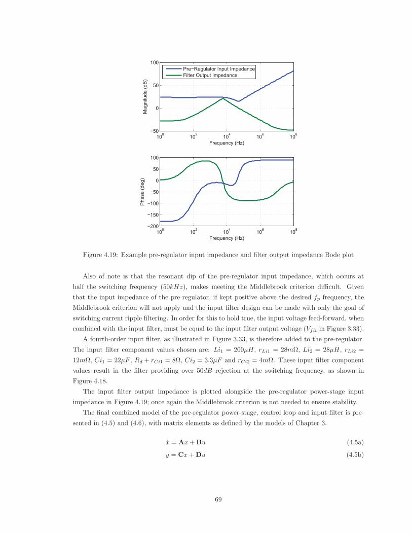
100 102 104 106 108−50
0
50
100
Mag
nitu
de (d
B)
Frequency (Hz)
Pre−Regulator Input ImpedanceFilter Output Impedance
100 102 104 106 108−200
−150
−100
−50
0
50
100
Pha
se (d
eg)
Frequency (Hz)
Figure 4.19: Example pre-regulator input impedance and filter output impedance Bode plot
Also of note is that the resonant dip of the pre-regulator input impedance, which occurs at
half the switching frequency (50kHz), makes meeting the Middlebrook criterion difficult. Given
that the input impedance of the pre-regulator, if kept positive above the desired fp frequency, the
Middlebrook criterion will not apply and the input filter design can be made with only the goal of
switching current ripple filtering. In order for this to hold true, the input voltage feed-forward, when
combined with the input filter, must be equal to the input filter output voltage (Vflt in Figure 3.33).
A fourth-order input filter, as illustrated in Figure 3.33, is therefore added to the pre-regulator.
The input filter component values chosen are: Li1 = 200μH, rLi1 = 28mΩ, Li2 = 28μH, rLi2 =
12mΩ, Ci1 = 22μF , Rd + rCi1 = 8Ω, Ci2 = 3.3μF and rCi2 = 4mΩ. These input filter component
values result in the filter providing over 50dB rejection at the switching frequency, as shown in
Figure 4.18.
The input filter output impedance is plotted alongside the pre-regulator power-stage input
impedance in Figure 4.19; once again the Middlebrook criterion is not needed to ensure stability.
The final combined model of the pre-regulator power-stage, control loop and input filter is pre-
sented in (4.5) and (4.6), with matrix elements as defined by the models of Chapter 3.
x = Ax+Bu (4.5a)
y = Cx+Du (4.5b)
69

x =
⎡⎢⎢⎢⎢⎢⎢⎢⎢⎢⎢⎢⎢⎢⎢⎣
iLi1
iLi2
vCi1
vCi2
iL
vC
d
ictl
⎤⎥⎥⎥⎥⎥⎥⎥⎥⎥⎥⎥⎥⎥⎥⎦
, y =
[vout
iin
], u =
⎡⎢⎢⎣vd
vctl
io
⎤⎥⎥⎦ (4.5c)
A =
[A1,1 A1,2
A2,1 A2,2
](4.6a)
A1,1 =
⎡⎢⎢⎢⎢⎣− rCi1+rLi1+Rd
Li1rCi1+Rd
Li1− 1
Li10
rCi1+Rd
Li2− rCi1+rCi2+rLi2+Rd
Li21
Li2− 1
Li21
Ci1− 1
Ci10 0
0 1Ci2
0 0
⎤⎥⎥⎥⎥⎦ (4.6b)
A1,2 =
⎡⎢⎢⎢⎢⎣
0 0 0 0c2,1rCi2
Li2
c2,2rCi2
Li2
c2,3rCi2
Li20
0 0 0 0
− c2,1Ci2
− c2,2Ci2
− c2,3Ci2
0
⎤⎥⎥⎥⎥⎦ (4.6c)
A2,1 =
⎡⎢⎢⎢⎢⎣0 b1,1rCi2 0 b1,1
0 b2,1rCi2 0 b2,1
0 (b3,1 +Kffb3,2) rCi2 0 b3,1 +Kffb3,2
0 0 0 0
⎤⎥⎥⎥⎥⎦ (4.6d)
A2,2 =
⎡⎢⎢⎢⎢⎣a1,1 − b1,1c2,1rCi2 a1,2 − b1,1c2,2rCi2 a1,3 − b1,1c2,3rCi2 b1,2
a2,1 − b2,1c2,1rCi2 a2,2 − b2,1c2,2rCi2 a2,3 − b2,1c2,3rCi2 b2,2
k1 k2 k3 b3,2
0 0 0 0
⎤⎥⎥⎥⎥⎦ (4.6e)
k1 = a3,1 −Kpb3,2c1,1 − (b3,1 +Kffb3,2) c2,1rCi2 (4.6f)
k2 = a3,2 −Kpb3,2c1,2 − (b3,1 +Kffb3,2) c2,2rCi2 (4.6g)
k3 = a3,3 − (b3,1 +Kffb3,2) c2,3rCi2 (4.6h)
B =
⎡⎢⎢⎢⎢⎢⎢⎢⎢⎢⎢⎢⎢⎢⎢⎣
1Li1
0 0
0 0 0
0 0 0
0 0 0
0 0 b1,3
0 0 b2,3
0 0 b3,3
0 Ki 0
⎤⎥⎥⎥⎥⎥⎥⎥⎥⎥⎥⎥⎥⎥⎥⎦
(4.6i)
70
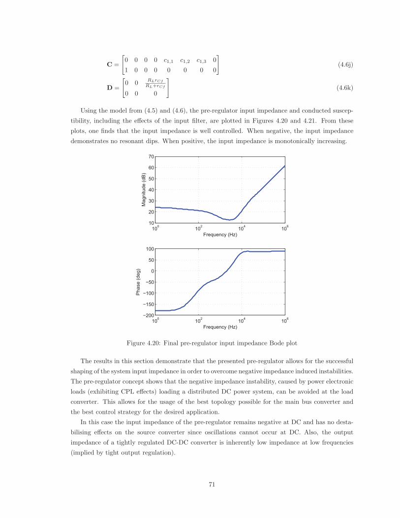
C =
[0 0 0 0 c1,1 c1,2 c1,3 0
1 0 0 0 0 0 0 0
](4.6j)
D =
[0 0
RLrCf
RL+rCf
0 0 0
](4.6k)
Using the model from (4.5) and (4.6), the pre-regulator input impedance and conducted suscep-
tibility, including the effects of the input filter, are plotted in Figures 4.20 and 4.21. From these
plots, one finds that the input impedance is well controlled. When negative, the input impedance
demonstrates no resonant dips. When positive, the input impedance is monotonically increasing.
100 102 104 10610
20
30
40
50
60
70
Mag
nitu
de (d
B)
Frequency (Hz)
100 102 104 106−200
−150
−100
−50
0
50
100
Pha
se (d
eg)
Frequency (Hz)
Figure 4.20: Final pre-regulator input impedance Bode plot
The results in this section demonstrate that the presented pre-regulator allows for the successful
shaping of the system input impedance in order to overcome negative impedance induced instabilities.
The pre-regulator concept shows that the negative impedance instability, caused by power electronic
loads (exhibiting CPL effects) loading a distributed DC power system, can be avoided at the load
converter. This allows for the usage of the best topology possible for the main bus converter and
the best control strategy for the desired application.
In this case the input impedance of the pre-regulator remains negative at DC and has no desta-
bilising effects on the source converter since oscillations cannot occur at DC. Also, the output
impedance of a tightly regulated DC-DC converter is inherently low impedance at low frequencies
(implied by tight output regulation).
71
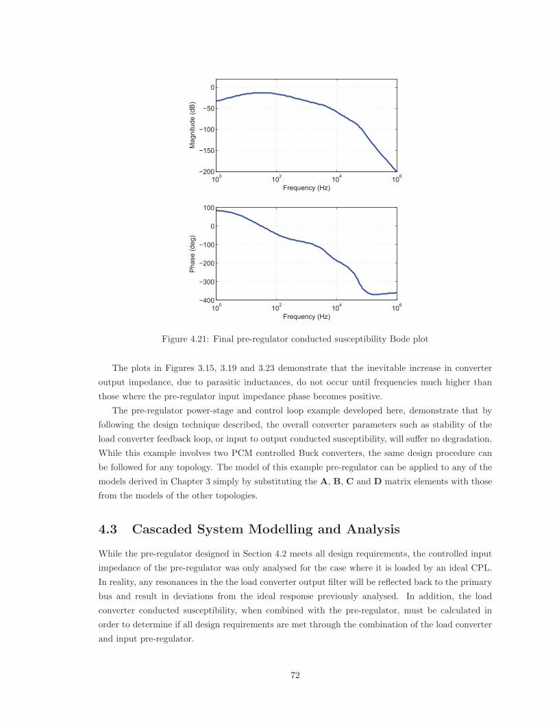
100 102 104 106−200
−150
−100
−50
0
Mag
nitu
de (d
B)
Frequency (Hz)
100 102 104 106−400
−300
−200
−100
0
100
Pha
se (d
eg)
Frequency (Hz)
Figure 4.21: Final pre-regulator conducted susceptibility Bode plot
The plots in Figures 3.15, 3.19 and 3.23 demonstrate that the inevitable increase in converter
output impedance, due to parasitic inductances, do not occur until frequencies much higher than
those where the pre-regulator input impedance phase becomes positive.
The pre-regulator power-stage and control loop example developed here, demonstrate that by
following the design technique described, the overall converter parameters such as stability of the
load converter feedback loop, or input to output conducted susceptibility, will suffer no degradation.
While this example involves two PCM controlled Buck converters, the same design procedure can
be followed for any topology. The model of this example pre-regulator can be applied to any of the
models derived in Chapter 3 simply by substituting the A, B, C and D matrix elements with those
from the models of the other topologies.
4.3 Cascaded System Modelling and Analysis
While the pre-regulator designed in Section 4.2 meets all design requirements, the controlled input
impedance of the pre-regulator was only analysed for the case where it is loaded by an ideal CPL.
In reality, any resonances in the the load converter output filter will be reflected back to the primary
bus and result in deviations from the ideal response previously analysed. In addition, the load
converter conducted susceptibility, when combined with the pre-regulator, must be calculated in
order to determine if all design requirements are met through the combination of the load converter
and input pre-regulator.
72

To accommodate these two aforementioned requirements, this section will model the cascaded
converter system including the input filter, pre-regulator and load converter. From this model,
the final loop responses of the pre-regulator and load converter can be analysed for stability. In
addition, the overall combined input to output conducted susceptibility of the cascaded system can
be obtained. Finally, an accurate input impedance of the complete system will be determined and
compared to the ideal results of Section 4.2.
4.3.1 Modelling the Cascaded System
The simplified schematic of the cascaded system, composed of the pre-regulator and load converter, is
shown in Figure 4.22. The pre-regulator component values (Cf1, rCf1, Lf1, rLf1, etc.) are defined
to be equal to the values discussed in Sections 4.2.2 through 4.2.5. Likewise, the load converter
component values (Cf2, rCf2, Lf2, rLf2, etc.) are defined to be equal those in Section 4.2.1.
Figure 4.22: Cascaded pre-regulator and load converter simplified schematic
In order to derive the model of the full cascaded pre-regulator and load converter system, the
models of each separate converter can be combined with the addition of two simple substitutions.
For the first simplification, io (input signal of the pre-regulator) must be substituted by −iin (output
signal of the load converter). For the second simplification, vd (input signal of the load converter)
must be substituted by vout (output signal of the pre-regulator), which will herein be referred to as
vlink (the DC-link voltage between converters). This is to avoid confusion with the overall system
output voltage.
The assumption that rCf1 � RL1 is also made to simplify the model derivation and represents the
worst case condition where the pre-regulator is primarily loaded by the load converter CPL. Using
this assumption, and following the aforementioned substitutions, results in the complete model of the
cascaded system, presented in (4.7) and (4.8). Using the notation followed in (4.8) the pre-regulator
model matrix components are given by a1m,n, b1m,n and c1m,n and the load converter model matrix
components are a2m,n, b2m,n and c2m,n.
x = Ax+Bu (4.7a)
y = Cx+Du (4.7b)
73
x =
⎡⎢⎢⎢⎢⎢⎢⎢⎢⎢⎢⎢⎢⎢⎢⎢⎢⎢⎢⎢⎢⎢⎢⎢⎢⎢⎢⎢⎣
iLi1
iLi2
vCi1
vCi2
iL1
vC1
d1
ictl1
iL2
vC2
d2
ictl2∫vctl2
⎤⎥⎥⎥⎥⎥⎥⎥⎥⎥⎥⎥⎥⎥⎥⎥⎥⎥⎥⎥⎥⎥⎥⎥⎥⎥⎥⎥⎦
, y =
⎡⎢⎢⎣vout
iin
vlink
⎤⎥⎥⎦ , u =
⎡⎢⎢⎢⎢⎣
vd
vctl1
vctl2
io
⎤⎥⎥⎥⎥⎦ (4.7c)
A =
⎡⎢⎢⎣A1,1 A1,2 04x5
A2,1 A2,2 A2,3
05x4 A3,2 A3,3
⎤⎥⎥⎦ (4.8a)
A1,1 =
⎡⎢⎢⎢⎢⎣− rCi1+rLi1+Rd
Li1rCi1+Rd
Li1− 1
Li10
rCi1+Rd
Li2− rCi1+rCi2+rLi2+Rd
Li21
Li2− 1
Li21
Ci1− 1
Ci10 0
0 1Ci2
0 0
⎤⎥⎥⎥⎥⎦ (4.8b)
A1,2 =
⎡⎢⎢⎢⎢⎣
0 0 0 0c12,1rCi2
Li2
c12,2rCi2
Li2
c12,3rCi2
Li20
0 0 0 0
− c12,1Ci2
− c12,2Ci2
− c12,3Ci2
0
⎤⎥⎥⎥⎥⎦ (4.8c)
A2,1 =
⎡⎢⎢⎢⎢⎣0 b11,1rCi2 0 b11,1
0 b12,1rCi2 0 b12,1
0 (b13,1 +Kffb13,2) rCi2 0 b13,1 +Kffb13,2
0 0 0 0
⎤⎥⎥⎥⎥⎦ (4.8d)
A2,2 =
⎡⎢⎢⎢⎢⎣a11,1 − b11,1c12,1rCi2 a11,2 − b11,1c12,2rCi2 a11,3 − b11,1c12,3rCi2 b11,2
a12,1 − b12,1c12,1rCi2 a12,2 − b12,1c12,2rCi2 a12,3 − b12,1c12,3rCi2 b12,2
k1 k2 k3 b13,2
0 0 0 0
⎤⎥⎥⎥⎥⎦ (4.8e)
k1 = a13,1 −Kpb13,2c11,1 − (b13,1 +Kffb13,2) c12,1rCi2 (4.8f)
k2 = a13,2 −Kpb13,2c11,2 − (b13,1 +Kffb13,2) c12,2rCi2 (4.8g)
k3 = a13,3 − (b13,1 +Kffb13,2) c12,3rCi2 (4.8h)
74
A2,3 =
⎡⎢⎢⎢⎢⎣−b11,3c22,1 −b11,3c22,2 −b11,3c22,3 0 0
−b12,3c22,1 −b12,3c22,2 −b12,3c22,3 0 0
−b13,3c22,1 −b13,3c22,2 −b13,3c22,3 0 0
0 0 0 0 0
⎤⎥⎥⎥⎥⎦ (4.8i)
A3,2 =
⎡⎢⎢⎢⎢⎢⎢⎢⎣
b21,1c11,1 b21,1c11,2 b21,1c11,3 0
b22,1c11,1 b22,1c11,2 b22,1c11,3 0
b23,1c11,1 b23,1c11,2 b23,1c11,3 0
0 0 0 0
0 0 0 0
⎤⎥⎥⎥⎥⎥⎥⎥⎦
(4.8j)
A3,3 =
⎡⎢⎢⎢⎢⎢⎢⎢⎣
a21,1 − rCf1b21,1c11,1 a21,2 − rCf1b21,1c11,2 a21,3 − rCf1b21,1c11,3 b21,2 0
a22,1 − rCf1b22,1c11,1 a22,2 − rCf1b22,1c11,2 a22,3 − rCf1b22,1c11,3 b22,2 0
a23,1 − rCf1b23,1c11,1 a23,2 − rCf1b23,1c11,2 a23,3 − rCf1b23,1c11,3 b23,2 0
0 0 0 −1R2C2
1R1R2C1C2
0 0 0 0 0
⎤⎥⎥⎥⎥⎥⎥⎥⎦
(4.8k)
B =
⎡⎢⎢⎢⎢⎢⎢⎢⎢⎢⎢⎢⎢⎢⎢⎢⎢⎢⎢⎢⎢⎢⎢⎢⎢⎢⎢⎢⎣
1Li1
0 0 0
0 0 0 0
0 0 0 0
0 0 0 0
0 0 0 0
0 0 0 0
0 0 0 0
0 Ki 0 0
0 0 0 b21,3
0 0 0 b22,3
0 0 0 b23,3
0 0 1R1C2
0
0 0 1 0
⎤⎥⎥⎥⎥⎥⎥⎥⎥⎥⎥⎥⎥⎥⎥⎥⎥⎥⎥⎥⎥⎥⎥⎥⎥⎥⎥⎥⎦
(4.8l)
C =
⎡⎢⎢⎣0 0 0 0 0 0 0 0 c21,1 c21,2 c21,3 0 0
1 0 0 0 0 0 0 0 0 0 0 0 0
0 0 0 0 c11,1 c11,2 c11,3 0 0 0 0 0 0
⎤⎥⎥⎦ (4.8m)
D =
⎡⎢⎢⎣0 0 0
RL2rCf2
RL2+rCf2
0 0 0 0
0 0 0 0
⎤⎥⎥⎦ (4.8n)
While the example chosen involves two cascaded Buck converters, the pre-regulator design steps
and cascaded system modelling methodology can be equally used for any combination of power-
stage topology design. Modelling of these example cascaded current-mode controlled power-stages,
illustrates the versatility of the models developed in Chapter 3.
75
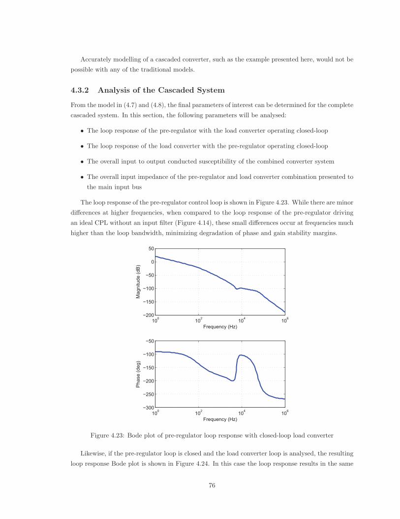
Accurately modelling of a cascaded converter, such as the example presented here, would not be
possible with any of the traditional models.
4.3.2 Analysis of the Cascaded System
From the model in (4.7) and (4.8), the final parameters of interest can be determined for the complete
cascaded system. In this section, the following parameters will be analysed:
• The loop response of the pre-regulator with the load converter operating closed-loop
• The loop response of the load converter with the pre-regulator operating closed-loop
• The overall input to output conducted susceptibility of the combined converter system
• The overall input impedance of the pre-regulator and load converter combination presented to
the main input bus
The loop response of the pre-regulator control loop is shown in Figure 4.23. While there are minor
differences at higher frequencies, when compared to the loop response of the pre-regulator driving
an ideal CPL without an input filter (Figure 4.14), these small differences occur at frequencies much
higher than the loop bandwidth, minimizing degradation of phase and gain stability margins.
100 102 104 106−200
−150
−100
−50
0
50
Mag
nitu
de (d
B)
Frequency (Hz)
100 102 104 106−300
−250
−200
−150
−100
−50
Pha
se (d
eg)
Frequency (Hz)
Figure 4.23: Bode plot of pre-regulator loop response with closed-loop load converter
Likewise, if the pre-regulator loop is closed and the load converter loop is analysed, the resulting
loop response Bode plot is shown in Figure 4.24. In this case the loop response results in the same
76
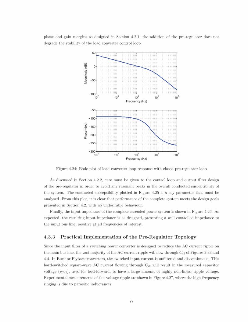
phase and gain margins as designed in Section 4.2.1; the addition of the pre-regulator does not
degrade the stability of the load converter control loop.
102 103 104 105 106−100
−50
0
50
Mag
nitu
de (d
B)
Frequency (Hz)
102 103 104 105 106−300
−250
−200
−150
−100
−50
Pha
se (d
eg)
Frequency (Hz)
Figure 4.24: Bode plot of load converter loop response with closed pre-regulator loop
As discussed in Section 4.2.2, care must be given to the control loop and output filter design
of the pre-regulator in order to avoid any resonant peaks in the overall conducted susceptibility of
the system. The conducted susceptibility plotted in Figure 4.25 is a key parameter that must be
analysed. From this plot, it is clear that performance of the complete system meets the design goals
presented in Section 4.2, with no undesirable behaviour.
Finally, the input impedance of the complete cascaded power system is shown in Figure 4.26. As
expected, the resulting input impedance is as designed, presenting a well controlled impedance to
the input bus line; positive at all frequencies of interest.
4.3.3 Practical Implementation of the Pre-Regulator Topology
Since the input filter of a switching power converter is designed to reduce the AC current ripple on
the main bus line, the vast majority of the AC current ripple will flow through Ci2 of Figures 3.33 and
4.4. In Buck or Flyback converters, the switched input current is unfiltered and discontinuous. This
hard-switched square-wave AC current flowing through Ci2 will result in the measured capacitor
voltage (vCi2), used for feed-forward, to have a large amount of highly non-linear ripple voltage.
Experimental measurements of this voltage ripple are shown in Figure 4.27, where the high-frequency
ringing is due to parasitic inductances.
77
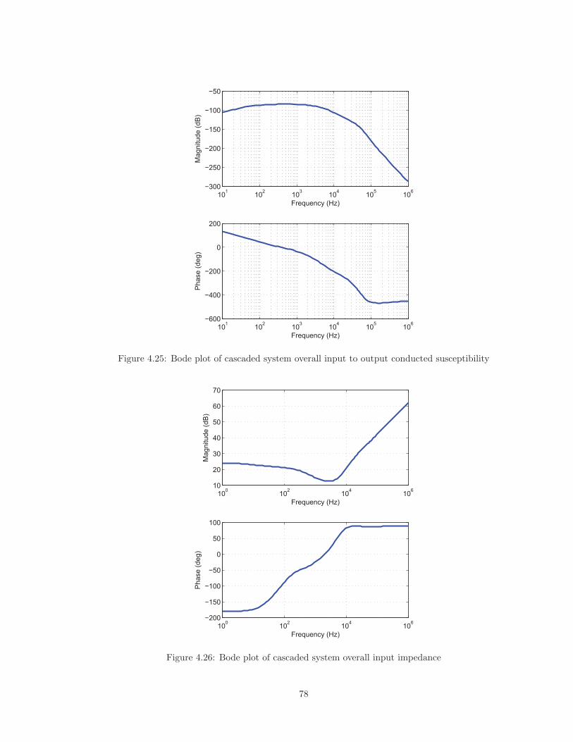
101 102 103 104 105 106−300
−250
−200
−150
−100
−50
Mag
nitu
de (d
B)
Frequency (Hz)
101 102 103 104 105 106−600
−400
−200
0
200
Pha
se (d
eg)
Frequency (Hz)
Figure 4.25: Bode plot of cascaded system overall input to output conducted susceptibility
100 102 104 10610
20
30
40
50
60
70
Mag
nitu
de (d
B)
Frequency (Hz)
100 102 104 106−200
−150
−100
−50
0
50
100
Pha
se (d
eg)
Frequency (Hz)
Figure 4.26: Bode plot of cascaded system overall input impedance
78
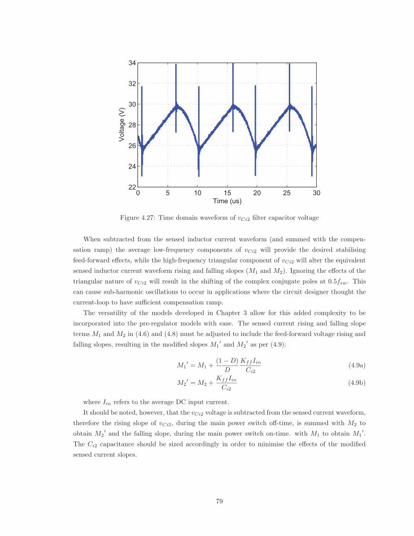
0 5 10 15 20 25 3022
24
26
28
30
32
34
Vol
tage
(V)
Time (us)
Figure 4.27: Time domain waveform of vCi2 filter capacitor voltage
When subtracted from the sensed inductor current waveform (and summed with the compen-
sation ramp) the average low-frequency components of vCi2 will provide the desired stabilising
feed-forward effects, while the high-frequency triangular component of vCi2 will alter the equivalent
sensed inductor current waveform rising and falling slopes (M1 and M2). Ignoring the effects of the
triangular nature of vCi2 will result in the shifting of the complex conjugate poles at 0.5fsw. This
can cause sub-harmonic oscillations to occur in applications where the circuit designer thought the
current-loop to have sufficient compensation ramp.
The versatility of the models developed in Chapter 3 allow for this added complexity to be
incorporated into the pre-regulator models with ease. The sensed current rising and falling slope
terms M1 and M2 in (4.6) and (4.8) must be adjusted to include the feed-forward voltage rising and
falling slopes, resulting in the modified slopes M1′ and M2
′ as per (4.9):
M1′ = M1 +
(1−D)
D
KffIinCi2
(4.9a)
M2′ = M2 +
KffIinCi2
(4.9b)
where Iin refers to the average DC input current.
It should be noted, however, that the vCi2 voltage is subtracted from the sensed current waveform,
therefore the rising slope of vCi2, during the main power switch off-time, is summed with M2 to
obtain M2′ and the falling slope, during the main power switch on-time. with M1 to obtain M1
′.
The Ci2 capacitance should be sized accordingly in order to minimise the effects of the modified
sensed current slopes.
79
While the above applies to the Flyback, Buck, and Buck-derived converters such as the Forward
converter. Inductor input converters such as the Boost or SEPIC topologies have continuous input
currents, reducing the vCi2 ripple voltage. For such inductor input topologies, the adjusted M1′ and
M2′ terms are not required in order to accurately model the pre-regulator.
This fact, combined with the lower required Cf1 pre-regulator filter capacitances, results in the
Boost topology being the most desirable for pre-regulator design.
4.3.4 Validation of the Cascaded System Model
The pre-regulator topology introduced in Section 4.1 was modelled in Section 4.3.2 using the method-
ology discussed in Chapter 3. The added non-linearities introduced to the feed-forward due to dis-
continuities in the input current of the Buck and Flyback topologies were explored in Section 4.3.3,
where their effects were included into the previously derived models. In this section, the time domain
results obtained from the aforementioned models will be compared with measured results, validating
the models and the pre-regulator design.
Figures 4.28 and 4.29 plot the modelled and measured DC-link voltage (Vlink) waveforms when
the output of the load converter is subjected to a 1A square-wave step-load with a repetition rate
of 10Hz. While the DC-link voltage exhibits overshoot, the output of the load converter is tightly
regulated and does not experience significant ripple due to it’s much higher loop bandwidth (fc =
15kHz for this example). While the output impedance of the pre-regulator need not be designed
to stabilise the system as with previous methods, care must be taken to ensure that overshoot does
not exceed the voltage rating of components used. The DC-link voltage overshoot concerns can be
mitigated by using higher voltage DC-link voltages, through the use of step-up converters, such as
the Boost or Flyback.
The waveforms in Figures 4.28 and 4.29 are nearly the same, exhibiting similar overshoot and
settling time, validating the models presented and the frequency domain analysis of Section 4.3.2.
Figures 4.30 and 4.31 compare the modelled and measured DC-link voltage (Vlink) waveforms
for the case where the input bus voltage is summed with a 1Vpk−pk 500Hz sine wave voltage source.
The results demonstrate the conducted susceptibility of the pre-regulator and illustrate the amount
of voltage ripple at the DC-link voltage due to the input voltage feed-forward gain. The amount
of ripple voltage present must be taken into account when selecting the power-stage components
and their associated voltage ratings. Once again the measured and modelled results match closely,
with the obvious exception of the switching waveform ripple not being modelled by the state space
averaged model.
Finally, the main design goal of the pre-regulator is to present a positive input impedance to
the main bus at frequencies where the load converter is tightly regulated. While the load converter
has an input impedance with −180◦ phase, the plots shown in Figures 4.32 and 4.33 show that the
input current is no longer negative and introduces no destabilising effects on the main DC bus. The
amplitudes and phases of the modelled and measured input currents, once again, match very closely,
further validating the modelling techniques used.
80
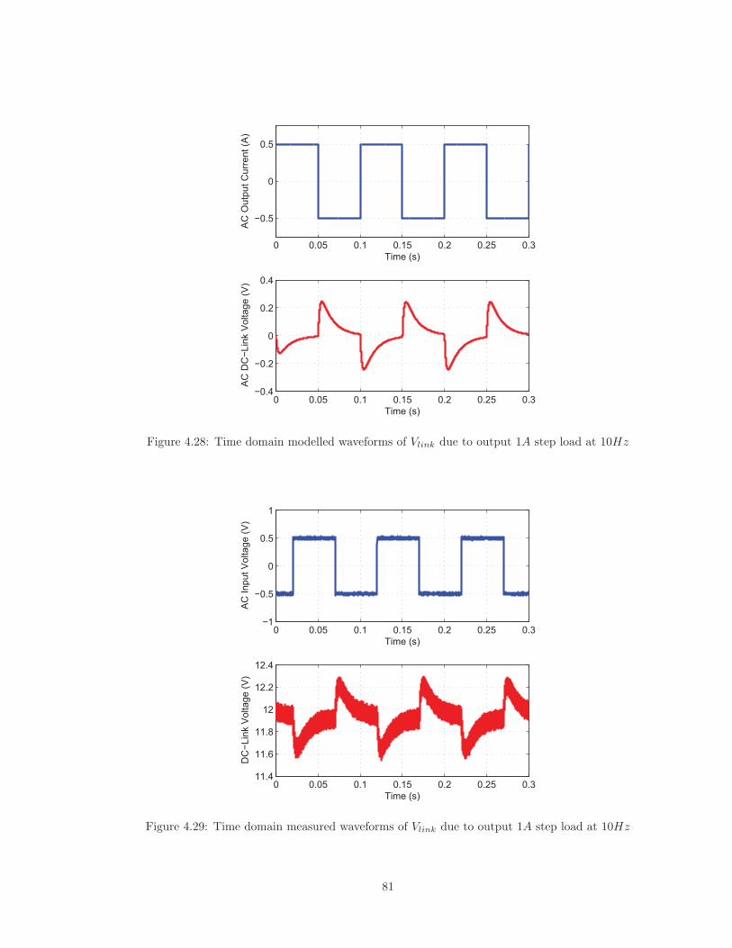
0 0.05 0.1 0.15 0.2 0.25 0.3
−0.5
0
0.5
AC
Out
put C
urre
nt (A
)Time (s)
0 0.05 0.1 0.15 0.2 0.25 0.3−0.4
−0.2
0
0.2
0.4
AC
DC−L
ink
Vol
tage
(V)
Time (s)
Figure 4.28: Time domain modelled waveforms of Vlink due to output 1A step load at 10Hz
0 0.05 0.1 0.15 0.2 0.25 0.3−1
−0.5
0
0.5
1
AC
Inpu
t Vol
tage
(V)
Time (s)
0 0.05 0.1 0.15 0.2 0.25 0.311.4
11.6
11.8
12
12.2
12.4
DC−L
ink
Vol
tage
(V)
Time (s)
Figure 4.29: Time domain measured waveforms of Vlink due to output 1A step load at 10Hz
81
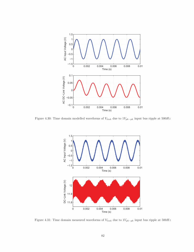
0 0.002 0.004 0.006 0.008 0.01−1.5
−1
−0.5
0
0.5
1
1.5
AC
Inpu
t Vol
tage
(V)
Time (s)
0 0.002 0.004 0.006 0.008 0.01−0.1
−0.05
0
0.05
0.1
AC
DC−L
ink
Vol
tage
(V)
Time (s)
Figure 4.30: Time domain modelled waveforms of Vlink due to 1Vpk−pk input bus ripple at 500Hz
0 0.002 0.004 0.006 0.008 0.01−1.5
−1
−0.5
0
0.5
1
1.5
AC
Inpu
t Vol
tage
(V)
Time (s)
0 0.002 0.004 0.006 0.008 0.01
11.8
11.9
12
DC−L
ink
Vol
tage
(V)
Time (s)
Figure 4.31: Time domain measured waveforms of Vlink due to 1Vpk−pk input bus ripple at 500Hz
82
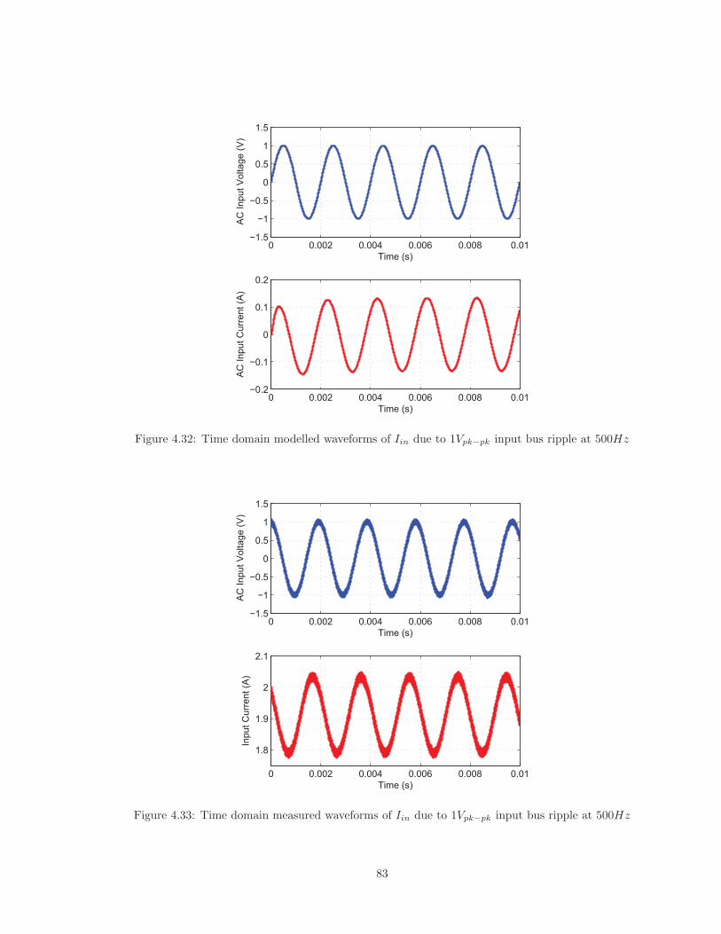
0 0.002 0.004 0.006 0.008 0.01−1.5
−1
−0.5
0
0.5
1
1.5
AC
Inpu
t Vol
tage
(V)
Time (s)
0 0.002 0.004 0.006 0.008 0.01−0.2
−0.1
0
0.1
0.2
AC
Inpu
t Cur
rent
(A)
Time (s)
Figure 4.32: Time domain modelled waveforms of Iin due to 1Vpk−pk input bus ripple at 500Hz
0 0.002 0.004 0.006 0.008 0.01−1.5
−1
−0.5
0
0.5
1
1.5
AC
Inpu
t Vol
tage
(V)
Time (s)
0 0.002 0.004 0.006 0.008 0.01
1.8
1.9
2
2.1
Inpu
t Cur
rent
(A)
Time (s)
Figure 4.33: Time domain measured waveforms of Iin due to 1Vpk−pk input bus ripple at 500Hz
83

In conclusion, the pre-regulator concept introduced and analysed in the this chapter, allows for a
power supply designer to shape the input impedance of a high-bandwidth DC-DC power converter to
appear positive at low frequencies. This positive input impedance stabilises the otherwise unstable
distributed DC system when loaded by the load converter stage directly. The design steps presented
allow for the load converter to be designed independently from the pre-regulator power-stage and
control loop. Furthermore, it was demonstrated that the performance of the load converter is in no
way impaired by the introduction of the pre-regulator. The models derived in Chapter 3 allow for
the straight forward design, and accurate modelling, of the pre-regulator stage. Finally, the time
domain simulation results obtained using the models from Chapter 3 were compared with measured
results, validating the modelling methods and pre-regulator design.
84
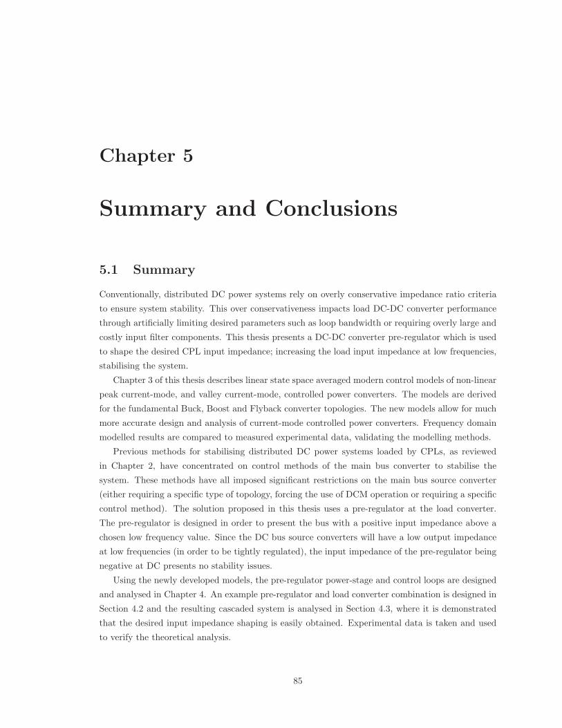
Chapter 5
Summary and Conclusions
5.1 Summary
Conventionally, distributed DC power systems rely on overly conservative impedance ratio criteria
to ensure system stability. This over conservativeness impacts load DC-DC converter performance
through artificially limiting desired parameters such as loop bandwidth or requiring overly large and
costly input filter components. This thesis presents a DC-DC converter pre-regulator which is used
to shape the desired CPL input impedance; increasing the load input impedance at low frequencies,
stabilising the system.
Chapter 3 of this thesis describes linear state space averaged modern control models of non-linear
peak current-mode, and valley current-mode, controlled power converters. The models are derived
for the fundamental Buck, Boost and Flyback converter topologies. The new models allow for much
more accurate design and analysis of current-mode controlled power converters. Frequency domain
modelled results are compared to measured experimental data, validating the modelling methods.
Previous methods for stabilising distributed DC power systems loaded by CPLs, as reviewed
in Chapter 2, have concentrated on control methods of the main bus converter to stabilise the
system. These methods have all imposed significant restrictions on the main bus source converter
(either requiring a specific type of topology, forcing the use of DCM operation or requiring a specific
control method). The solution proposed in this thesis uses a pre-regulator at the load converter.
The pre-regulator is designed in order to present the bus with a positive input impedance above a
chosen low frequency value. Since the DC bus source converters will have a low output impedance
at low frequencies (in order to be tightly regulated), the input impedance of the pre-regulator being
negative at DC presents no stability issues.
Using the newly developed models, the pre-regulator power-stage and control loops are designed
and analysed in Chapter 4. An example pre-regulator and load converter combination is designed in
Section 4.2 and the resulting cascaded system is analysed in Section 4.3, where it is demonstrated
that the desired input impedance shaping is easily obtained. Experimental data is taken and used
to verify the theoretical analysis.
85
5.2 Conclusions
The input impedance shaping pre-regulator concept introduced in this thesis allows for the stabili-
sation of distributed DC power systems loaded by CPLs. By controlling the CPL input impedance,
forcing it to be positive above a desired frequency, distributed DC power system designers are al-
lowed to choose the best main bus converter topology and control strategy for the application. This
shaping of the CPL input impedance allows for power-supply designers to stabilise distributed DC
power systems without artificially limiting load converter performance.
The presented pre-regulator allows for the load converters to also be designed independently from
the main bus output impedance, allowing for higher loop bandwidths and smaller input filters. The
pre-regulator approach also has the added benefit, over all other discussed methods, of stabilising
unregulated DC buses loaded by heavy CPLs. The developed stabilising approach can be used in
conjunction with any of the impedance ratio criteria mentioned in Chapter 2; this is very important
in situations where the load converters are developed independent from the bus.
The state space averaged models of peak and valley current-mode controlled power converters,
derived in this work, provide more accurate predictions of power converter performance than existing
methods. Modelling of the controlled duty cycle ratio of constant-frequency current-mode control as
the third system state, results in a description (through state-variable feedback techniques) of the
stabilising properties of the compensation ramp.
The versatility of these new models allow for the inclusion of controller propagation delays, input
filter effects and closed voltage-loops. Furthermore, the modern control theory used allowed for the
modelling of cascaded DC-DC converters (Chapter 4). Through the use of this new modelling
approach the design and accurate analysis of the pre-regulator, presented here, becomes possible.
5.3 Suggestions for Future Work
As an extension to the research work presented in this thesis, the following topics are suggested:
i Expand the state space averaged current-mode control models to describe higher-order converter
topologies such as SEPIC and Cuk converters.
ii Expand the constant-frequency models of current-mode control to include constant on-time and
constant off-time current-mode control.
iii Analyse the potential benefits of operating the pre-regulator power-stage in DCM.
iv Analyse single-stage PFC techniques to determine the feasibility of similarly combining the pre-
regulator and load converters into a single-switch converter.
86

Bibliography
[1] A. Riccobono and E. Santi, “Comprehensive review of stability criteria for dc distribution
systems,” in Energy Conversion Congress and Exposition (ECCE), 2012 IEEE, pp. 3917–3925,
Sept 2012.
[2] Y. Jang and R. Erickson, “Physical origins of input filter oscillations in current programmed
converters,” Power Electronics, IEEE Transactions on, vol. 7, pp. 725–733, Oct 1992.
[3] A. Riccobono and E. Santi, “Comprehensive review of stability criteria for dc power distribution
systems,” Industry Applications, IEEE Transactions on, vol. PP, no. 99, pp. 1–1, 2014.
[4] R. Middlebrook, “Input filter considerations in design and application of switching regulators,”
IEEE IAS Annual Meeting, 1976.
[5] C. Wildrick, F. Lee, B. Cho, and B. Choi, “A method of defining the load impedance specifica-
tion for a stable distributed power system,” Power Electronics, IEEE Transactions on, vol. 10,
pp. 280–285, May 1995.
[6] X. Feng, J. Liu, and F. Lee, “Impedance specifications for stable dc distributed power systems,”
Power Electronics, IEEE Transactions on, vol. 17, pp. 157–162, Mar 2002.
[7] S. Sudhoff, S. Glover, P. Lamm, D. H. Schmucker, and D. Delisle, “Admittance space stability
analysis of power electronic systems,” Aerospace and Electronic Systems, IEEE Transactions
on, vol. 36, pp. 965–973, Jul 2000.
[8] S. Sudhoff and J. Crider, “Advancements in generalized immittance based stability analysis
of dc power electronics based distribution systems,” in Electric Ship Technologies Symposium
(ESTS), 2011 IEEE, pp. 207–212, April 2011.
[9] X. Wang, R. Yao, and F. Rao, “Three-step impedance criterion for small-signal stability analysis
in two-stage dc distributed power systems,” Power Electronics Letters, IEEE, vol. 1, pp. 83–87,
Sept 2003.
[10] A. Emadi, A. Khaligh, C. Rivetta, and G. Williamson, “Constant power loads and negative
impedance instability in automotive systems: definition, modeling, stability, and control of
power electronic converters and motor drives,” Vehicular Technology, IEEE Transactions on,
vol. 55, pp. 1112 –1125, july 2006.
87

[11] W. Wei, X. Haiping, W. Xuhui, and S. Wenqing, “Dynamics and control of electronic cascaded
systems,” in Power Electronics and Motion Control Conference, 2006. IPEMC 2006. CES/IEEE
5th International, vol. 1, pp. 1 –4, aug. 2006.
[12] V. Grigore, J. Hatonen, J. Kyyra, and T. Suntio, “Dynamics of a buck converter with a constant
power load,” in Power Electronics Specialists Conference, 1998. PESC 98 Record. 29th Annual
IEEE, vol. 1, pp. 72 –78 vol.1, may 1998.
[13] C. Rivetta, G. Williamson, and A. Emadi, “Constant power loads and negative impedance
instability in sea and undersea vehicles: statement of the problem and comprehensive large-
signal solution,” in Electric Ship Technologies Symposium, 2005 IEEE, pp. 313 – 320, july
2005.
[14] N. Mohan, W. P. Robbins, and T. Undeland, Power electronics: converters, applications and
design; 3rd ed. New York, NY: Wiley, 2003.
[15] R. C. Dorf and R. H. Bishop, Modern control systems; 11th ed. Upper Saddle River, NJ:
Pearson, 2003.
[16] A. Rahimi and A. Emadi, “Active damping in dc/dc power electronic converters: A novel
method to overcome the problems of constant power loads,” Industrial Electronics, IEEE Trans-
actions on, vol. 56, pp. 1428 –1439, may 2009.
[17] A. Rahimi, G. Williamson, and A. Emadi, “Loop-cancellation technique: A novel nonlinear
feedback to overcome the destabilizing effect of constant-power loads,” Vehicular Technology,
IEEE Transactions on, vol. 59, pp. 650 –661, feb. 2010.
[18] A. Khaligh, A. Rahimi, and A. Emadi, “Modified pulse-adjustment technique to control dc/dc
converters driving variable constant-power loads,” Industrial Electronics, IEEE Transactions
on, vol. 55, pp. 1133 –1146, march 2008.
[19] H. Xu, X. Wen, and T. Lipo, “Digital charge control of boost converter with constant power ma-
chine load,” in Electrical Machines and Systems, 2008. ICEMS 2008. International Conference
on, pp. 999 –1004, oct. 2008.
[20] W. Tang, F. Lee, R. Ridley, and I. Cohen, “Charge control: modeling, analysis, and design,”
Power Electronics, IEEE Transactions on, vol. 8, pp. 396 –403, oct 1993.
[21] S. Kim and S. Williamson, “Negative impedance instability compensation in more electric
aircraft dc power systems using state space pole placement control,” in Vehicle Power and
Propulsion Conference (VPPC), 2011 IEEE, pp. 1 –6, sept. 2011.
[22] Y. Zhao and W. Qiao, “A third-order sliding-mode controller for dc/dc converters with constant
power loads,” in Industry Applications Society Annual Meeting (IAS), 2011 IEEE, pp. 1 –8,
oct. 2011.
88
[23] I. Kondratiev, E. Santi, R. Dougal, and G. Veselov, “Synergetic control for dc-dc buck converters
with constant power load,” in Power Electronics Specialists Conference, 2004. PESC 04. 2004
IEEE 35th Annual, vol. 5, pp. 3758 – 3764 Vol.5, june 2004.
[24] X. Feng, Z. Ye, K. Xing, F. Lee, and D. Borojevic, “Individual load impedance specification for
a stable dc distributed power system,” in Applied Power Electronics Conference and Exposition,
1999. APEC ’99. Fourteenth Annual, vol. 2, pp. 923 –929 vol.2, mar 1999.
[25] M. de Brito, L. Galotto, L. Sampaio, G. de Azevedo e Melo, and C. Canesin, “Evaluation of the
main mppt techniques for photovoltaic applications,” Industrial Electronics, IEEE Transactions
on, vol. 60, pp. 1156–1167, March 2013.
[26] O. Semiconductor, Power Factor Correction (PFC) Handbook; Rev. 4. Denver, CO: ON Semi-
conductor, 2011.
[27] M. Hallworth and S. Shirsavar, “Microcontroller-based peak current mode control using digital
slope compensation,” Power Electronics, IEEE Transactions on, vol. 27, no. 7, pp. 3340–3351,
2012.
[28] C. Restrepo, J. Calvente, A. Romero, E. Vidal-Idiarte, and R. Giral, “Current-mode control of a
coupled-inductor buck-boost dc-dc switching converter,” Power Electronics, IEEE Transactions
on, vol. 27, no. 5, pp. 2536–2549, 2012.
[29] R. Ridley, “An accurate and practical small-signal model for current-mode control,” Ridley
Engineering, Inc., 1999.
[30] Y. Yan, F. Lee, and P. Mattavelli, “Comparison of small signal characteristics in current mode
control schemes for point-of-load buck converter applications,” Power Electronics, IEEE Trans-
actions on, vol. 28, no. 7, pp. 3405–3414, 2013.
[31] S. Cuk and R. Middlebrook, “A general unified approach to modelling switching-converter
power stages,” Power Electronics Specialists Conference, 1976. PESC ’76 Record, pp. 18 –34,
Jun 1976.
[32] R. Tymerski and D. Li, “State space models for current programmed pulse width modulated
converters,” in Power Electronics Specialists Conference, 1992. PESC ’92 Record., 23rd Annual
IEEE, pp. 337–344 vol.1, Jun 1992.
[33] T. Pavlovic, T. Bjazic, and Z. Ban, “Simplified averaged models of dc-dc power converters
suitable for controller design and microgrid simulation,” Power Electronics, IEEE Transactions
on, vol. 28, no. 7, pp. 3266–3275, 2013.
[34] R. Ridley, “A new continuous-time model for current-mode control with constant frequency,
constant on-time, and constant off-time, in ccm and dcm,” in Power Electronics Specialists
Conference, 1990. PESC ’90 Record., 21st Annual IEEE, pp. 382 –389, 0-0 1990.
89
[35] N. Kondrath and M. Kazimierczuk, “Audio-susceptibility of the inner-loop of peak current-
mode controlled pwm dc-dc buck converter in ccm,” in IECON 2012 - 38th Annual Conference
on IEEE Industrial Electronics Society, pp. 250–255, 2012.
[36] G. Chu, D. Lu, and V. Agelidis, “Practical application of valley current mode control in a
flyback converter with a large duty cycle,” Power Electronics, IET, vol. 5, pp. 552–560, May
2012.
[37] J.-M. Liu, P.-Y. Wang, and T.-H. Kuo, “A current-mode dc-dc buck converter with efficiency-
optimized frequency control and reconfigurable compensation,” Power Electronics, IEEE Trans-
actions on, vol. 27, no. 2, pp. 869–880, 2012.
[38] C. Basso, Switch-Mode Power Supplies Spice Simulations and Practical Designs. New York,
NY, USA: McGraw-Hill, Inc., 1 ed., 2008.
[39] T. Suntio, D. Gadoura, and K. Zenger, “Input filter interactions in current-mode controlled
converters-a unified analysis approach,” in IECON 02 [Industrial Electronics Society, IEEE
2002 28th Annual Conference of the], vol. 2, pp. 1179–1184 vol.2, Nov 2002.
[40] F. Tan and R. Middlebrook, “A unified model for current-programmed converters,” Power
Electronics, IEEE Transactions on, vol. 10, pp. 397 –408, jul 1995.
[41] R. Tymerski and D. Li, “State-space models for current programmed pulsewidth-modulated
converters,” Power Electronics, IEEE Transactions on, vol. 8, pp. 271–278, Jul 1993.
[42] T. Qi and J. Sun, “Single-phase pfc control using pwm-based multipliers,” in Power Electronics
and Motion Control Conference, 2009. IPEMC ’09. IEEE 6th International, pp. 660–665, May
2009.
[43] D. Izquierdo, R. Azcona, F. del Cerro, C. Fernandez, and B. Delicado, “Electrical power distri-
bution system (hv270dc), for application in more electric aircraft,” in Applied Power Electron-
ics Conference and Exposition (APEC), 2010 Twenty-Fifth Annual IEEE, pp. 1300 –1305, feb.
2010.
90

![State Space Modelling of Current-Mode Control and its ... · filter and power converter combinations [4]. The Middlebrook stability criterion states that the output impedance of](https://img.pdfslide.us/doc/110x75/5ea0b41a86c072739f057264/state-space-modelling-of-current-mode-control-and-its-ilter-and-power-converter.jpg)


![Kit terena-space-between-lavacon [compatibility mode]](https://img.pdfslide.us/doc/110x75/55890f79d8b42a966e8b4684/kit-terena-space-between-lavacon-compatibility-mode.jpg)