Embed Size (px)
Citation preview

Starting Materials and Functional Layers for The 2005 International Technology
Roadmap for Semiconductors: Challenges and Opportunities
Howard R. Huff(a), David Myers(b), Mike Walden(c), Larry Beckwith(d), Neil Weaver(e), George Celler(f),
Bob Standley(g) and Mayank T. Bulsara(h)
Starting Materials and Functional Layers for The 2005 International Technology
Roadmap for Semiconductors: Challenges and Opportunities
Howard R. Huff(a), David Myers(b), Mike Walden(c), Larry Beckwith(d), Neil Weaver(e), George Celler(f),
Bob Standley(g) and Mayank T. Bulsara(h)
(a) SEMATECH(b) Texas Instruments, retired(c) SUMCO(d) National Semiconductor(e) SEH(f) SOITEC-USA(g) MEMC(h) Amberwave Systems
2005 International Conference on Characterization and Metrology for ULSI TechnologyMarch 17, 2005

2005 International Conference on Characterization and Metrology for ULSI TechnologyMarch 17, 2005
Starting Materials Team MembersStarting Materials Team Members
Physical Models & Statistical Distributions Polished / Epitaxial Wafer SOI Wafer Metrology Emerging Materials
Larry Beckwith (Ntl'l) Olli Anttila (Okmetic Oyj) Michael Alles (Vanderbilt U.) George Brown (ISMT) Mayank T. Bulsara (AmberWave)
W. Murray Bullis (Mtls & Metrology) Joel Barnett (ISMT) Luis Aparicio (Siltronic) Laszlo Fabry (Siltronic) George Celler (SOITEC)
Bill Hughes (MEMC) Juanita Chambers (Siltronic) Mayank T. Bulsara (AmberWave) Dick Hockett (Charles Evans) * Bruce Kellerman (MEMC)
Mototaka Kamoshida (NEC Tokin) *Roxanne Dulas (Siltronic) George Celler (SOITEC) Noel Poduje (ADE) Lalita Manchanda (SRC/Agere)
Paul Langer (Komatsu) Graham Fisher (MEMC) Michael Current (FSM) Chris Sparks (ISMT) Jim Moreland (Siltronic)
Don McCormack (ISMT) Glenn Gale (TEL) * Harry Hovel (IBM) Bob Standley (MEMC) Doug Meyer (ATMI)
Noel Poduje (ADE) Dinesh Gupta (STA) Sien Kang (SiGen) Carl Treadwell (KLA-Tencor) Bob Standley (MEMC)
Kevin Han (TSMC) Jerry Liu (ADE) Peter Wagner (Siltronic) * Neil Weaver (SEH)
Bob Johnston (SUMCO) Stephane Monfray (ST Micro) Rick Wise (TI)
Susanne Weizbauer (Infineon) Helmut Oefner (Infineon) Ted White (Freescale Semiconductor)
Wen Lin (Consultant) Gerd Pfeiffer (IBM)
Tom McKenna (TI) K.V. Ravi (Intel)
Fred Meyer (Komatsu) Ted White (Freescale Semiconductor)
Dave Myers (Consultant)
Pete Sandrow (LG Siltron)
Jack Thomas (AMD)
Neil Weaver (SEH)
Masaharu Watanabe (NuFlare)
* Corresponding Member
Howard Huff (ISMT) - Chair ; Mike Walden (SUMCO) - Co-Chair

2005 International Conference on Characterization and Metrology for ULSI TechnologyMarch 17, 2005
AgendaAgenda• Introduction
• Challenges– Site Flatness and Nanotopography– Particle Size – Wafer Edge Exclusion / Roll-Off– 450 mm Diameter Wafers
• Opportunities– SOI– Strained Silicon (and Ge)– Hybrid Structures
• Actions

2005 International Conference on Characterization and Metrology for ULSI TechnologyMarch 17, 2005
Transistors to Integrated CircuitsTransistors to Integrated Circuits
Used with permission of the Estate of John Bardeen Reproduced by Permission of the IEEE, Inc.
Reproduced by Permission of the IEEE, Inc.Courtesy of Texas Instruments, Inc.

2005 International Conference on Characterization and Metrology for ULSI TechnologyMarch 17, 2005
Simplified Cross-Section of MOSFET Transistor StructureSimplified Cross-Section of MOSFET Transistor Structure
Upper interfacial region
Bulk high-k film
Lower interfacial region
Gate electrode, poly
Si Substrate (or SOI with Si
thickness ≈1/3 Lg)
Source Drain
Spacer
High-k Gate Dielectric Stack
Lg
Modified From P.M. Zeitzoff, R.W. Murto and H.R. Huff, Solid State Technology, July 2002

2005 International Conference on Characterization and Metrology for ULSI TechnologyMarch 17, 2005
Transistor Scaling
Egs
SiGateDielectric
Ig
Band offsetGate
Electrode
Source Drain
Gate Dielectric
ISAT
Ig
t
SiGate Electrode
t
Requirement: Increase Isat ∝ µ·ε/t without increasing Ig ∝ exp(-tφn)

2005 International Conference on Characterization and Metrology for ULSI TechnologyMarch 17, 2005
AgendaAgenda• Introduction
• Challenges– Site Flatness and Nanotopography– Particle Size– Wafer Edge Exclusion / Roll-Off– 450 mm Diameter Wafers
• Opportunities– SOI– Strained Silicon (and Ge)– Hybrid Structures
• Actions

2005 International Conference on Characterization and Metrology for ULSI TechnologyMarch 17, 2005
Site Flatness and NanotopographySite Flatness and Nanotopography
• Appears 25 mm x 25 mm site still relevant trend – SFSR still not standardized or widely accepted / used
• Bi-modal distribution of SFQR (survey result)– SFQR ≈ technology generation
– SFQR significantly relaxed (≈ 40% larger than technology generation)
• Determination of nanotopography criticality– Dipole characteristic, IDMs either very interested or not
interested at all

2005 International Conference on Characterization and Metrology for ULSI TechnologyMarch 17, 2005
Critical Starting Materials: New IssuesCritical Starting Materials: New Issues• Chuck – Wafer Flatness Interaction
– Nature of chuck-wafer interaction is a 3-D challenge, especially dependent on leveling mechanism of chuck and chuck design in edge region, the latter affecting ability to obtain zero defocus
– Wide range of wafer chucks makes it virtually impossible for wafer suppliers to implement 100% chucked-wafer measurement
• Wear of chucks in fabs exacerbates chuck flatness /chuck-wafer interaction
– Recommend further discussion of relevant issues through SEMI
• Emerging Materials Focus (in 2003 ITRS revision)– Novel structures and processing methods to enhance silicon-based CMOS
technology to achieve ITRS device metrics – Strained silicon and its embodiments (metrology)
• Bulk strained Si (on uniform SiGe on compositionally graded SiGe) • Strained Si on uniform SiGe on Insulator (SGOI) – partially / fully depleted• Strained silicon on insulator (SSOI) or Ge – partially / fully depleted
– Other areas under consideration include Ge MOSFET structures, high-resistivity silicon, isotopically pure silicon and integrated optoelectronics on silicon

2005 International Conference on Characterization and Metrology for ULSI TechnologyMarch 17, 2005
Particle Size Reduction – Some User InputParticle Size Reduction – Some User Input• “Folly to reduce particle size to ½ technology generation
– Absolute nonsense from many points of view, including necessity and metrology
– Surface preparation should increase their size to one technologygeneration (or even larger)”
• “Numerous process steps leading to pre-gate level exceptionally convoluted
– Incoming wafer may play only a limited role in performance• Beyond actual processing steps which offer ready particle sources,
effect of in-line metrology cannot be discounted – Although same piece of silicon enters process, it clearly changes over time– From Starting Materials perspective, not obvious that two teams must
publish equivalent trends in ITRS tables• Many existence proofs, based upon actual customer specifications,
particles ≥ one technology generation ample to meet requirements”• Nevertheless, Surface Preparation claims IDMs indeed
need / require particle size = ½ technology generation

2005 International Conference on Characterization and Metrology for ULSI TechnologyMarch 17, 2005
Defect Density ChallengesDefect Density Challenges• Assess viability of continued utilization of
Maly equation to calculate defect density, kill ratio assumption as well as identification of appropriate kill ratio
– Y = exp [-DP R AActive Chip]
• Viability of utilizing square law relation
– D2 / D1 = (Tech. Gen.1 / Tech. Gen.2 )2
• Should we list values of defects appropriate to variously configured SOI and other Emerging Material structural configurations?– Some guidance and trends appear to be useful

2005 International Conference on Characterization and Metrology for ULSI TechnologyMarch 17, 2005
Critical Starting Materials (Old Issue Re-Addressed)Critical Starting Materials (Old Issue Re-Addressed)
• Surface Preparation sub-TWG has noted– Starting Materials methodology of increasing particles
and metals (by 2x the Maly derived value) enhances expectation that Surface Preparation can surely remove these increased levels
– Wrong message may be sent to suppliers of cleans equipment who have to deal with in-line (pre-gate) requirements (i.e., Surface Preparation) and yet work with wafers that are “looser” in incoming metal and particle levels

2005 International Conference on Characterization and Metrology for ULSI TechnologyMarch 17, 2005
Wafer Edge ExclusionWafer Edge Exclusion
• Edge exclusion (EE) needs to be consistent for Starting Materials, Yield Enhancement and Factory Integration(FI)
– ITRS Governing Body decision:
– Factory Integration decides EE - die/wafer
– Some types of SOI structures are currently incapable of achieving the 1mm EE mandated by FI
• ITRS denotes what perceived to be needed, even if tool is not yet available, per se

2005 International Conference on Characterization and Metrology for ULSI TechnologyMarch 17, 2005
Wafer RollWafer Roll--Off Off –– Possible Impact on NGLPossible Impact on NGL
Courtesy M. WatanabeCourtesy M. Watanabe

2005 International Conference on Characterization and Metrology for ULSI TechnologyMarch 17, 2005
Wafer RollWafer Roll--Off Off
Courtesy M. WatanabeCourtesy M. Watanabe

2005 International Conference on Characterization and Metrology for ULSI TechnologyMarch 17, 2005
Courtesy M. WatanabeCourtesy M. Watanabe
Wafer RollWafer Roll--OffOff

2005 International Conference on Characterization and Metrology for ULSI TechnologyMarch 17, 2005
450mm
• Periodic wafer diameter increases key element in remaining on Moore’s law– “When the wafer area increases by >2 times, but the
cost of the new tool set for the same number of wafer starts increases by only 30-40% (which is typical), the cost per area decreases by 30-50% --an annualized improvement of ~4% when wafer size changes occur about every 10 years.”R. Goodall, D. Fandel, A. Allan, P. Landler, and H. Huff,Semiconductor Silicon/2002, ECS PV 2002-2, 125-143 (2002)
• However, it is also imperative to be cognizant of starting wafer cost as the expected timing of transition may intersect ITRS at a point where non-standard material types are predominant
D. Myers, Microelectronic Materials Strategy Symposium, SEMI, San Jose, CA, 9/24/02.

2005 International Conference on Characterization and Metrology for ULSI TechnologyMarch 17, 2005
450mm450mm• Very useful to maintain two year technology cycle
– Migration to three year technology cycle may be likely• Will nanotechnology-based manufacturing paradigm
facilitate off-the-roadmap perspective and obviate 450mm diameter perceived need
– Extrapolation forward (business as usual) hoping world not change
• Need further assessment of assumptions related to perceived wafer diameter change
– Nine year wafer diameter development cycle previously noted
– Therefore, we may already be somewhat behind for 2011 450mm diameter wafer assessment at IDMs

2005 International Conference on Characterization and Metrology for ULSI TechnologyMarch 17, 2005
450mm (cont.)450mm (cont.)
• Assess potential alternatives to wafer diameter change
• Role / impact of emerging technologies requires consideration
• 450mm anticipated to present severe financial crisis for silicon and equipment suppliers– Changes in functionality of automated material
handling system (AMHS) not fully comprehended• Although ITRS fundamental technology trend
guide for industry, it does not directly address economic factors– Consequence of strict adherence to historic trends
without utmost due diligence represents clear issue to viability of IC industry

2005 International Conference on Characterization and Metrology for ULSI TechnologyMarch 17, 2005
Connecting Economic & Technology ChallengesConnecting Economic & Technology Challenges
• Industry strategy for next wafer size transition to include:– Initial concepts for fab design, operations, and integration– Supply chain impact and key intercept points– Timing & cost of transition
• ISMI View, based on Member Company feedback (July-04)– Further modeling and analysis needed– Must leverage all TWGs addressing the issue– Too early for substantial resource commitments
ISMIISMI

2005 International Conference on Characterization and Metrology for ULSI TechnologyMarch 17, 2005
450mm (cont.)450mm (cont.)• Is 2012 appropriate for 450mm / how funded?
– How and when will issue(s) and decision(s) be resolved– Need further discussion and more serious consideration for
alternative solutions to productivity enhancement• Fundamental diameter issues addressed by ITRS
Tables are for 300 mm but MANY IDM’s have announced aggressive geometry production on 200mm (90 nm technology generations and potentially beyond)
• If SOI and 450mm both become necessary at about same time things could become very interesting – May be unlikely, however, since SOI seems more poised for
implementation than 450mm (and is indeed impacting available wafer substrate types in market-place)

2005 International Conference on Characterization and Metrology for ULSI TechnologyMarch 17, 2005
Learnings From 300mm Experience?Learnings From 300mm Experience?– Establish earlier consensus on fab architecture &
operations • One company driving strategy is suboptimal • Need to comprehend wafer size bridging in toolset
– Drive business models and architectural strategies• Leave supply chain pricing to the market
– Develop standards early to reduce costs– Support multiple leading-edge operational modes
• High-volume/low-mix, High-volume/high-mix, etc.– Continuously evaluate and adjust, including:
• Impact of technology on next wafer size transition timing• Tradeoffs and timing using modeling and simulation
tools– Industry coordination is crucial and valuable
ISMIISMI

2005 International Conference on Characterization and Metrology for ULSI TechnologyMarch 17, 2005
Critical Starting Materials: New IssuesCritical Starting Materials: New Issues• Chuck – Wafer Flatness Interaction
– Nature of chuck-wafer interaction is a 3-D challenge, especially dependent on leveling mechanism of chuck and chuck design in edge region, latter affecting ability to obtain zero defocus
– Wide range of wafer chucks makes it virtually impossible for wafer suppliers to implement 100% chucked-wafer measurement
• Wear of chucks in fabs exacerbates chuck flatness /chuck-wafer interaction
– Recommend further discussion of relevant issues through SEMI
• Emerging Materials Focus (in 2003 ITRS revision)– Novel structures and processing methods to enhance silicon-based CMOS
technology to achieve ITRS device metrics – Strained silicon and its embodiments (metrology)
• Bulk strained Si (on uniform SiGe on compositionally graded SiGe) • Strained Si on uniform SiGe on Insulator (SGOI) – partially / fully depleted• Strained silicon on insulator (SSOI) or Ge – partially / fully depleted
– Other areas under consideration include Ge MOSFET structures, high-resistivity silicon, isotopically pure silicon and integrated optoelectronics on silicon

2005 International Conference on Characterization and Metrology for ULSI TechnologyMarch 17, 2005
AgendaAgenda• Introduction
• Challenges– Site Flatness and Nanotopography– Particle Size– Wafer Edge Exclusion / Roll-Off– 450 mm Diameter Wafers
• Opportunities– SOI– Strained Silicon (and Ge) – Global versus Local– Hybrid Structures
• Actions

2005 International Conference on Characterization and Metrology for ULSI TechnologyMarch 17, 2005
Transistor StructuresTransistor Structures
G
Planar Bulk Partially Depleted Fully DepletedSOI SOI
2. Mark Bohr, ECS Meeting PV 2001-2, Spring, 2001
+ Lower junction cap- SCE scaling difficult- High Rseries,s/d⇒raisedS/D
- Sensitivity to Si thickness (very thin)
- Wafer cost/availability
G
Substrate
BOX
SD
SD
Substrate
Buried Oxide (BOX)
+ Lower junction cap+ F.B. performance
boost- F.B. history effect- SCE scaling difficult- Wafer cost/availability
SD
G
Substrate
Depletion Region
+ Wafer cost / availability- SCE scaling difficult- High doping effects and statistical variation
- Parasitic junction capacitance
References:1. P. Zeitzoff, J. Hutchby and H. Huff, Internat. Jour. High Speed Electronics & Systems

2005 International Conference on Characterization and Metrology for ULSI TechnologyMarch 17, 2005
Tri-gate Relaxes TSi Requirement of Single-gateTri-gate Relaxes TSi Requirement of Single-gate
Courtesy of Robert Chau et al., ISSDM, 2002

2005 International Conference on Characterization and Metrology for ULSI TechnologyMarch 17, 2005
Tri-gate Relaxes WSi Requirement of Double-gateTri-gate Relaxes WSi Requirement of Double-gate
Courtesy of Robert Chau et al., ISSDM, 2002
2005 International Conference on Characterization and Metrology for ULSI TechnologyMarch 17, 2005
Potential Solutions: 2004 UpdateChanged SOI to clear colorization in 2004 and cross-hatched shading in 2006 to ensure consistency with commercial reality
Potential Solutions: 2004 UpdateChanged SOI to clear colorization in 2004 and cross-hatched shading in 2006 to ensure consistency with commercial reality
First Year of IC Production 200310 0 nm
20049 0 nm
20058 0 nm
20067 0 nm
20076 5 nm
20085 7 nm
20095 0 nm
20104 5 nm
20114 0 nm
20123 5 nm
20133 2 nm
20143 0 nm
20152 5 nm
20162 2 nm
20172 0 nm
201818 nm 2019
300m m Leading Edge Materials Selection
Wafer Diam eter
Site Flatness
This legend indicates the time during which research, development, and qual i fication/pre-production should be tak ing place for the solution. Research RequiredDevelopment UnderwayQualification / Pre-ProductionContinuous Improvement
Work-in-Progress--Do Not Publish
CZ WafersDefect-engineered
CZ Wafers
Em erging Materials(Strained m aterials /layers , high res is tivity, etc.)
NewTech-nology
New Technology (Includes CMP; Orientation Dependent Etch;Localized Etch; Localized Deposition + blanket etch or CMP;Blanket layer + blanket etch or CMP)
NewTech-nology
Double-s ided Polish
675 m m 675 m m
450 m m 450 m m
Alternatives to large-Diameter Si Wafers
(Includes novel subs tratesand new circuit approaches)
450 m m
SOI includes: • Bonded Wafers • SIMOX Wafers • Selective SOI areas w ithin the IC chip
Defect EngineeredCZ Wafers include: • P/P+ and P/P++ epi • P/P- epi • Annealed Wafers • Slow pull/slow cool
SOIWafers
SOIWafers

2005 International Conference on Characterization and Metrology for ULSI TechnologyMarch 17, 2005
SOISOI
• SOI implementation will at some point become necessary to solve leakage issues that are limiting further reductions in feature size
• There will be a point at which it will not be possible to maintain shrink progression that enables Moore’s Law, without SOI
• Becomes a “timing” issue because there is question as to exactly when that point will come—as a matter of physics, economics, and technological readiness

2005 International Conference on Characterization and Metrology for ULSI TechnologyMarch 17, 2005
SOISOI• Economic issues are price of SOI wafers and timing
that each IC company uses for SOI implementation– Ideally should be implemented somewhat before becomes
physically impossible to otherwise progress, because there[is] a learning curve involved in maximizing its yield
• Technological readiness issues have to do with capabilities of SOI wafers, for example metrology limitations / film thickness uniformity concerns
• Resolution of some issues depend on device structures(i.e., FinFET) required when SOI becomes imperative
• Therefore, very important for industry to have an accurate forecast of which technology node will absolutely require SOI, from a physics standpoint

2005 International Conference on Characterization and Metrology for ULSI TechnologyMarch 17, 2005
Methods of Forming Strained Si / SGOI
Bonding and Layer Transfer
Thermal Mixing of SiGe with SOI
Integrated SIMOX-SGOI
Sadana / Current, SOI Technology Symposium,Oct. 18, 2004

2005 International Conference on Characterization and Metrology for ULSI TechnologyMarch 17, 2005
SSOI Substrate Fabrication ProcessSSOI Substrate Fabrication Process
Si Substrate
SiO2
Strained Si
Si Substrate
Graded SiGe
Relaxed SiGe
Si Substrate
SiO2
Strained SiRelaxed SiGe
Surface roughness reduction
Si Substrate
SiO2
Strained Si
Final StructureSubstrate RemovalWafer Bond
Starting material quality critical to process

2005 International Conference on Characterization and Metrology for ULSI TechnologyMarch 17, 2005
O Implantation Epi SiGe Growth
SiGe
1320°C SIMOX Anneal
Si
O & Damage
SiGeSiO2
Integrated SIMOX and SGOI Process
Must form a continuous BOX layer before Ge diffuses into bulk
Sadana / Current, SOI Technology Symposium,Oct. 18, 2004

2005 International Conference on Characterization and Metrology for ULSI TechnologyMarch 17, 2005
300 mm SGOI/Strain300 mm SGOI/Strain--SiSi FETFET
XTEM XTEM Sadana / Current, SOI Technology Symposium,Oct. 18, 2004

2005 International Conference on Characterization and Metrology for ULSI TechnologyMarch 17, 2005
Strained Silicon Motivation: MobilityStrained Silicon Motivation: Mobility
µ = ⏐e⏐ τ / m*
⏐e⏐= absolute value of electronic charge– τ = scattering rate– m* = effective mass
µ = δ v / ε
δ v = incremental speed gained per applied electric field ε

2005 International Conference on Characterization and Metrology for ULSI TechnologyMarch 17, 2005
Electron Mobility Enhancement in Strained Si MOSFETs (Rim,et al., IEDM 1998)
Vertical Effective Field, Eeff (MV/cm)0.00 0.25 0.50 0.75 1.00 1.25
Effe
ctiv
e E
lect
ron
Mob
ility
, µef
f (cm
2 / V s
ec)
0
200
400
600
800Strained Si onrelaxed Si0.8Ge0.2
Unstrained Si control
Universal Mobility(S. Takagi et. al., TED '94)
Welser et. al., IEDM '94
this work
Room T
• Electron mobility enhancement of ~ 1.8X persists up to high Eeff (~ 1MV/cm)• Strained-Si allows “moving off” universal mobility curve
Judy Hoyt, MIT

2005 International Conference on Characterization and Metrology for ULSI TechnologyMarch 17, 2005
Strain Effect on Carrier MobilityStrain Effect on Carrier Mobility
IBM, Rim et al, IEDM, Tech Dig, p. 49 (2003)

2005 International Conference on Characterization and Metrology for ULSI TechnologyMarch 17, 2005
Electron Transport in εMOS™Electron Transport in εMOS™
Unstrained
[001]
[010]
[100]
in-plane∆4 valleysperpendicular
∆2 valleys
BiaxialTension
Tensile strain splitsconduction band
degeneracy
• Reduced intervalley scattering• Light in-plane effective mass
[010]
[100]
[001]
Courtesy of Matt CurrieAmberWave Systems Corp.

2005 International Conference on Characterization and Metrology for ULSI TechnologyMarch 17, 2005
Hole Transport in εMOS™Hole Transport in εMOS™
E
kHeavy Hole
Light HoleSplit-Off
in-plane out-of-plane
Unstrained BiaxialTension
Tensile strain splitsvalence banddegeneracy
• Reduced intervalley scattering• Light in-plane effective mass
Courtesy of Matt CurrieAmberWave Systems Corp.
in-plane out-of-plane

2005 International Conference on Characterization and Metrology for ULSI TechnologyMarch 17, 2005
Key Strained Si Performance ResultsKey Strained Si Performance Results
• Many manufacturers have reported performance enhancements with strained Si– IBM, AMD, UMC, TSMC, Texas Instruments, Toshiba, Intel
• Strained silicon provides higher speed, lower power transistors than bulk silicon
– Compatibility with 45 nm - 130 nm DRs (depending on structure and device)
– Integrated with high K and metal gate
– Benefits for RF application
– 20% Id,sat enhancement demonstrated for Lg = 25nm
– > 30% ring oscillator performance enhancement reported

2005 International Conference on Characterization and Metrology for ULSI TechnologyMarch 17, 2005
Integration with High K and Metal GateIntegration with High K and Metal Gate
24% DC Id,sat enhancementwith good matching of Vt and subthreshold
INTEL, Datta, et al, IEDM, Tech. Dig., p. 653 (2003)

2005 International Conference on Characterization and Metrology for ULSI TechnologyMarch 17, 2005
NMOS Ion-Ioff BenefitNMOS Ion-Ioff Benefit
Lgate down to 60nm1.7 nm EOT
15% DC enhancementlargest ever reported
Correction for self heating adds approximately 10% more enhancement
TSMC, Wang et al, IEDM, Tech. Dig., p. 61 (2003)

2005 International Conference on Characterization and Metrology for ULSI TechnologyMarch 17, 2005
PMOS Ion-Ioff BenefitPMOS Ion-Ioff Benefit
11-19% enhancement due to strained Si
Toshiba, Sanuki et al, IEDM, Tech. Dig., p. 65 (2003)

2005 International Conference on Characterization and Metrology for ULSI TechnologyMarch 17, 2005
Localized (Uniaxial) Stress MethodsLocalized (Uniaxial) Stress Methods
Reproduced with the permission of M. Ieong et al., (IBM)

2005 International Conference on Characterization and Metrology for ULSI TechnologyMarch 17, 2005
Tensile / Compressive Stress RelationsTensile / Compressive Stress Relations
GateGate
Source Drain
GateGateGateGate
Source Drain
STI
Source DrainGat
e
Longitudinal
Tran
sver
se
Z
CCTTTTnFETnFET
TTCCTTpFETpFET
ZZLong.Long.Tran.Tran.
CCTTTTnFETnFET
TTCCTTpFETpFET
ZZLong.Long.Tran.Tran.
Desired Stress:
T: Tensile stressC: Compressive stress
Dependence of device performance on the types and directions of uni-axial stresses. Reproduced with the permission of M. Ieong et al., (IBM) and The Electrochemical Society, Inc.
2005 International Conference on Characterization and Metrology for ULSI TechnologyMarch 17, 2005
AgendaAgenda• Introduction
• Challenges– Site Flatness and Nanotopography– Particle Size– Wafer Edge Exclusion / Roll-Off– 450 mm Diameter Wafers
• Opportunities– SOI– Strained Silicon (and Ge)– Hybrid Structures
• Actions

2005 International Conference on Characterization and Metrology for ULSI TechnologyMarch 17, 2005
Orientation Effect on Effective Electron and Hole MobilityOrientation Effect on Effective Electron and Hole Mobility
(a)(a) (b)(b)(a)(a) (b)(b)
Orientation effect on the (a) effective electron mobility, (b) effective hole mobility as a function of inversion carrier density. Electron mobility is the highest on the (100) surface while the hole mobility on the (110) surface is more than 2.5 times higher than that on the (100) surface. Reproduced with the permission of M. Ieong et al., (IBM) and The Electrochemical Society, Inc.

2005 International Conference on Characterization and Metrology for ULSI TechnologyMarch 17, 2005
Hybrid OrientationTechnologyHybrid OrientationTechnology
Hybrid Orientation Technology (HOT). PFET on (110) surface and nFET on (100) surface. Planar structure, fully compatible with standard CMOS processes. Reproduced with permission of Min Yang et al., (IBM) and the IEEE (© 2003 IEEE).

2005 International Conference on Characterization and Metrology for ULSI TechnologyMarch 17, 2005
AgendaAgenda• Introduction
• Challenges– Site Flatness and Nanotopography– Particle Size– Wafer Edge Exclusion / Roll-Off– 450 mm Diameter Wafers
• Opportunities– SOI– Strained Silicon (and Ge)– Hybrid Structures
• Actions

2005 International Conference on Characterization and Metrology for ULSI TechnologyMarch 17, 2005
ActionsActions• Assess updated survey responses from IDMs for
2005 ITRS– 1:1 dialogue with silicon suppliers to ensure integrity of
silicon and SOI suppliers cell colorization andmanufacturing capability
• Significant loss of silicon mtl’s expertise in IDMsdue to evolving industrial focus on IC scaling
• Silicon suppliers expected to fill required research• Silicon suppliers are resource and extremely
financial limited• ‘Silicon still substrate for building these [non-
classical CMOS] devices’* although many components inside CMOS-like transistors will be very different, including many manufacturing processes* Ken David (Intel)
2005 International Conference on Characterization and Metrology for ULSI TechnologyMarch 17, 2005
AcknowledgementsAcknowledgements
• Surface Preparation, Thermal / Thin Films, PIDS, Yield Enhancement and Factory Integration ITRS TWGs
• ISMI personnel at SEMATECH
2005 International Conference on Characterization and Metrology for ULSI TechnologyMarch 17, 2005
Supplemental MaterialSupplemental Material

2005 International Conference on Characterization and Metrology for ULSI TechnologyMarch 17, 2005
Electrostatic Scaling of Classical CMOS Channel Leakage (Ioff)
TunnelingBTB
E VB
E CB
EmissionThermionic
QMTunneling
DrainSourceLgate
Substrate
Gate
Source Drain
Gate Leakage
Channel Leakage
Sum = Ioff
Channel Leakage
Jim Hutchby

2005 International Conference on Characterization and Metrology for ULSI TechnologyMarch 17, 2005
The Ideal MOS Transistor
2005 International Conference on Characterization and Metrology for ULSI TechnologyMarch 17, 2005
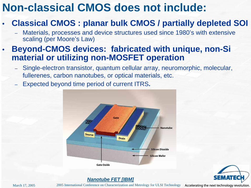
Non-classical CMOS does not include:Non-classical CMOS does not include:• Classical CMOS : planar bulk CMOS / partially depleted SOI
– Materials, processes and device structures used since 1980’s with extensive scaling (per Moore’s Law)
• Beyond-CMOS devices: fabricated with unique, non-Simaterial or utilizing non-MOSFET operation
– Single-electron transistor, quantum cellular array, neuromorphic, molecular, fullerenes, carbon nanotubes, or optical materials, etc.
– Expected beyond time period of current ITRS.
Nanotube FET [IBM]

2005 International Conference on Characterization and Metrology for ULSI TechnologyMarch 17, 2005
CMOL CONCEPT
molecular single-electron latching switch
Possible density: 3×10¹² functions per cm2
K. Likharev and A. Mayr, 2002(see http://rsfq1.physics.sunysb.edu/~likharev/nano/GigaNano010603.pdf)
longer bridge as an insulator/capacitor
diimide acceptor as an island
thiol group as an alligator clip
single-electron transistor
single-electron trap
S
S
N
NO
O
O
O
O
O
S
N
N
O O
O O
N
N
O O
O O
O
O
S
OPE bridge as a tunnel junction
Si substrate
SOI MOSFET
CMOS wiring
CMOSplug
SiO2 insulation
CMOS--to-MOL
plug
gold nanowires
gate
2005 International Conference on Characterization and Metrology for ULSI TechnologyMarch 17, 2005
Microelectronics RevolutionMicroelectronics Revolution
• Gordon Moore (a)– “But then you see the numbers or hear your
company’s name on the evening news … and you are once again reminded that this is no longer just an industry, but an economic and cultural phenomenon, a crucial force at the heart of the modern world.”
• Gordon Moore (b)– “No exponential is forever: but “forever” can
be delayed!”
(a) Beyond Imagination:Commemorating 25 Years, SIA (2002) [Introduction by Gordon Moore] (b) ISSCC 2003 / Session 1/ Plenary 1.1 (2003)

2005 International Conference on Characterization and Metrology for ULSI TechnologyMarch 17, 2005
Gordon MooreGordon Moore
H.R.Huff,J. Electrochem. Soc., 149, S35-S58 (2002) (© The ElectrochemicalSociety,Inc., reproduced
with permission)

2005 International Conference on Characterization and Metrology for ULSI TechnologyMarch 17, 2005
John BardeenJohn Bardeen
Courtesy of Lillian Hoddeson

2005 International Conference on Characterization and Metrology for ULSI TechnologyMarch 17, 2005
Bob DennardBob Dennard