Embed Size (px)
Citation preview

Wieman - CCAST - Workshop 1
STAR R&D and Detector Upgrade
Howard WiemanCCAST Workshop11-Aug-2004

Wieman - CCAST - Workshop 2
STAR Upgrade Projects
MRPC TOF Time of FlightHFT Heavy Flavor Tracker – Pixel micro-vertexInner TrackerForward TrackerDAQ1000FEE UpgradeVery Forward Cal

Wieman - CCAST - Workshop 3
MRPC TOF Time of Flight
RPC high granularity high resolution TOF systemTwo following talks:
Hong-Fang ChenYi Wang

Wieman - CCAST - Workshop 4
TOFmanagementchart
BNL project oversightT. Ludlam (BNL)
STAR Project oversightJ. Thomas (LBNL)
Project managerG. Eppley (Rice)
US-China coordinationH.Huang (UCLA)
Detectors and mech.W.J. LLope (Rice)
ElectronicsJ. Schambach (UT)
Board purchase/testT. Nussbaum (Rice)
Integration/system testT. Nussbaum (Rice)
Install/commissionJ. Schambach (UT)
Configuration/controlsoftware
Tray assembly/testJ. Hoffmann (UT)
Gas systemL. Kotchenda (MEPHI)
High voltageV. Ghazikhanian (UCLA)
Start detectorW.J. Llope (Rice)
InfrastructureD. Padrazo (BNL)
Low voltage systemV. Ghazikhanian (UCLA)

Wieman - CCAST - Workshop 5
China STAR TOF construction project
Project managerY. MaSINAP
Module productionJ. ChengTsinghua
Quality controlX. WangUSTC
Data analysisY. MaSINAP
Tsinghua productionY. Li
Tsinghua
Tsinghua QAY. WangTsinghua
USTC QAX. WangUSTC
Test softwareM. ShaoUSTC
IOPP data analysisF. LiuIOPP
USTC data analysisJ. WuUSTC
SINAP data analysisY. MaSINAP
USTC productionC. Li
USTC

Wieman - CCAST - Workshop 6
MRPC R&D
Six cellsCell area:
3.0cm×6.0cmGas gap:
6×0.22mm

Wieman - CCAST - Workshop 7
RPC

Wieman - CCAST - Workshop 8
Automated Fish Line Threader

Wieman - CCAST - Workshop 9
MRPC Future Production Facility

Wieman - CCAST - Workshop 10
TOF Development in the next run
TOFp and CAMAC daq will be removed for Run 5Run 5 is an engineering runFirst HPTDC useFirst use of ALICE PCI-PC based DAQNew start detector for Run 6, possibly ready for part of Run 5
Wieman - CCAST - Workshop 11
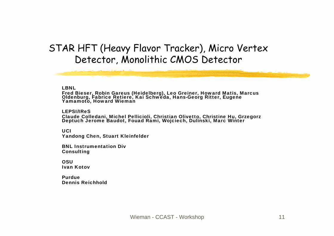
STAR HFT (Heavy Flavor Tracker), Micro Vertex Detector, Monolithic CMOS Detector
LBNLFred Bieser, Robin Gareus (Heidelberg), Leo Greiner, Howard Matis, Marcus Oldenburg, Fabrice Retiere, Kai Schweda, Hans-Georg Ritter, Eugene Yamamoto, Howard Wieman
LEPSI/IReSClaude Colledani, Michel Pellicioli, Christian Olivetto, Christine Hu, Grzegorz Deptuch Jerome Baudot, Fouad Rami, Wojciech, Dulinski, Marc Winter
UCIYandong Chen, Stuart Kleinfelder
BNL Instrumentation DivConsulting
OSUIvan Kotov
PurdueDennis Reichhold

Wieman - CCAST - Workshop 12
STAR Micro Vertex Detector
Two layers1.5 cm radius4 cm radius
24 ladders2 cm X 20 cm each30 µm X 30 µm pixels~ 100 Mega Pixels< 0.2% X010 µm position resolution

Wieman - CCAST - Workshop 13
Charm hadron reconstruction performances (figure of merit)
~1 M (φ+π+)
~100 M (φ+π+)
~1,000 M (φ+π+)
N events for 3 σ D+
s signalIn progress
10 K
100 K
2.6 M
12.6 M
N events for 3 σ D0
signal
TPC+SVT+µVertex+TOF
TPC+SVT+µVertex
TPC+SVT+TOF
TPC+SVT
System

Wieman - CCAST - Workshop 14
Sensors: Monolithic CMOS Active Pixel Sensors
AdvantagesPreciseCan be thinRather fastLow power
DisadvantagesSmall signalNot that fastNew
Need R&D
p-well p-welln-well
p-epi
p-substrate
5-20 µm
CMOS electronicAnalog & digital

Wieman - CCAST - Workshop 15
Electron hole pairs created in field free epi layerDiffusing electrons reflect off p boundary and collect on small n in p- epi diodesCollection time ~100nsRow and column selected with source follower readoutMinimum size diodes for good charge to voltage gain and minimum noise (1/C = 26 µV/e)
Monolithic CMOS detector, Active Pixel Sensor
P-
P
P+
Standard diode geometry
Standard APS diode structure

Wieman - CCAST - Workshop 16
APS monolithic CMOS
Active thickness 8 µmMost probable signal 450 eNoise ~17e, later development ~10eFit with Bichsel calculation
LBNL/UCI APS chipMeasured Signal amplitude distribution for 1.5 GeV/c electron beam

Wieman - CCAST - Workshop 17
MIMOSTAR LEPSI/IReS for first generation STAR detector
Based on MIMOSA-5, full wafer engineering run –significant readout infrastructure on chipLBNL test board works (Bieser and Gareus)
2 by 2 cm MIMOSA-5 chipLBNL development using 4 commercial 50 MHz 14 bit ADCs
MIMOSTAR Design1.9cmX1.9cm active30µmX 30µm pixels 409600 pixels/chipContinuous frame read at 4-8ms per frame52 mW per chipAnalogue readout options
Single fast option 50 to100 MHz10 at 10 MHz option

Wieman - CCAST - Workshop 18
Inner vertex detector in STAR
New vertex detector centered in pointing detector, supported one end only
End view showing 3 of 6 ladder modules
Conceptual design focused on rapid insertion and removal while preserving spatial mapping

Wieman - CCAST - Workshop 19
Support: Thin stiff ladder concept
Under developmentTested for thermal distortionWind tunnel vibration tests
carbon composite (75 µm)Young’s modulus 3-4 times steel
aluminum kapton cable(100 µm)
silicon chips(50 µm)
21.6 mm
254 mm

Wieman - CCAST - Workshop 20
TV Holography from ATLAS, LBNL
Lucite wind tunnelThin silicon ladder,tension support
Laser light source
Camera

Wieman - CCAST - Workshop 21
Capacitive Probe Measurement of Ladder Displacement and Vibration
wind tunnel box
ladder assembly
capacitive probe
air speedmeasurement device
fan
ends of box are open
10 deg. position
1.6 µm vibration
• Additional vibration measurements:High sensitivity accelerometer place of the STAR inner detector support structure

Wieman - CCAST - Workshop 22
Next Generation Monolithic CMOS Detector R&D
Goal: improve signal to noise and enable on chip zero suppressionPhoto-gate technology
Improve signal collectionOn the fly CDS
On pixel clamp circuit for CDSActive reset to remove fixed pattern noise and reset KTC noise

Wieman - CCAST - Workshop 23
photo gate
source follower gate
reset gate
transfer gate
row select gate
sense node drain
Large photo-gate to collect large fraction of the charge on a single pixel, directly on the p- epi layerSmall transfer gate also directly on p- epi layerSmall drain (minimum capacitance) connected to source follower gate (sense node)
Photo-gate geometry
20 µm
x -2 µm- 1 µm 1 µm5 nm
8 µm
0.1 µm
0.4 µm
P epi 1.4x10¹⁵ 1/cm3
N+ 1x10²⁰ 1/cm3
photo gate transfer gate
drain
x = 0.4 and 0.8 µm
(simulation quantities)

Wieman - CCAST - Workshop 24
Photo-gate issues in standard CMOS
No double poly process –possible poor transfer between gates because of low transverse field
Floating n well between gates, a bad solution to the transfer problem with single poly
Sub-micron process may solve problem
single poly, limitation of CMOS
double poly, standard for CCDs
photo gatetransfer gate drain
floating n well

Wieman - CCAST - Workshop 25
Photo gate/transfer gate operation (400 nm gap)
photogate
transgate1.8 V V
drain2.4 V
photogate
transgate
drain
V phg = 0.8 Vtransfer mode
V phg = 2.4 Vcollection mode

Wieman - CCAST - Workshop 26
Photo gate/transfer gate with 800 nm separation
photogate
transgate1.8 V V
drain2.4 V
photogate
transgate
drain
V phg = 0.8 Vtransfer mode
V phg = 2.4 Vcollection mode

Wieman - CCAST - Workshop 27
First silicon tests, comparing photo-gate with standard diode structure
Photo-gate directly to sense node drain
DC bias:V photo-gate 0.6 VV drain 2.4 V
Output signal for Fe55 X-ray test
Issue:
ADC
Linear
ADC
Log
diode
Photo-gate 1
Photo-gate 2
diode - fullcharge collection
Why is the signal spread out – is it surface traps under the gate?

Wieman - CCAST - Workshop 28
CDS clamp
kTC noise removed by clamp circuit – noise scales as
2CkT
Rather than
diodekTC

Wieman - CCAST - Workshop 29
Active reset
Signal from output is amplified to zero the inputIn test
Wieman - CCAST - Workshop 30
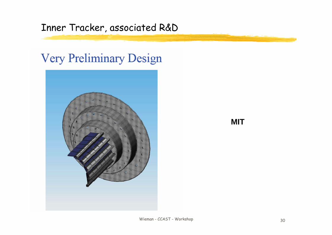
Inner Tracker, associated R&D
MIT

Wieman - CCAST - Workshop 31
Inner Tracker, associated R&D
Wieman - CCAST - Workshop 32
3GEM foil R&D work for Forward Tracker
N. Smirnov (Yale) , D. Majka (Yale), C. Woody (BNL), H. Spinka (ANL), D. Underwood (ANL), M. Plesko (MIT-
Bates), D. Hasell (MIT), Berndt Surrow (MIT)

Wieman - CCAST - Workshop 33
Outlook: Triple-GEM tile layout in GEANT (N. Smirnoff)
Triple-GEM activities

Wieman - CCAST - Workshop 34
CERN Tech-Etch
Contact to TechEtchTechEtch GEM foil

Wieman - CCAST - Workshop 35
GoalDesign of at least three triple-GEM chambers to be installed and tested at STAR under beam conditions:
Establish collaboration to a US company to develop and manufacture GEM foils for applications in triple-GEM detectors and other applications such as GEM TPC readout schemes Manufacture 2D-readout structuresDesign of a flexible GEM chamber to install and replace GEM foilsDesign of a chip readout system
R&D team:Collaboration between STAR/PHENIX: ANL, BNL, MIT, Yale
R&D and construction laboratory:In order to realize the design and construction of a GEM-type tracking detector for the RHIC collider experiments, a clean-room facility to handle, inspect and test GEM-foils besides the actual detector assembly is urgently needed
Strong interest by several MIT faculty and staff members to establish such a test and construction facility at LNS and MIT-Bates using two existing clean rooms setups used for the BLAST drift chamber construction Minimal effort to re-use existing clean rooms for GEM applications Profit from clean room experience at MIT Microsystems Technology Laboratory Several clean room accessories are available for free from the MIT Microsystems Technology Laboratory based on industry donations (Contact to Dr. Vicky Diadiuk, Assistant Director, MIT Microsystems Technology Laboratory)
Other potential location: Yale
Goal of the prototype triple-GEM effort
Wieman - CCAST - Workshop 36
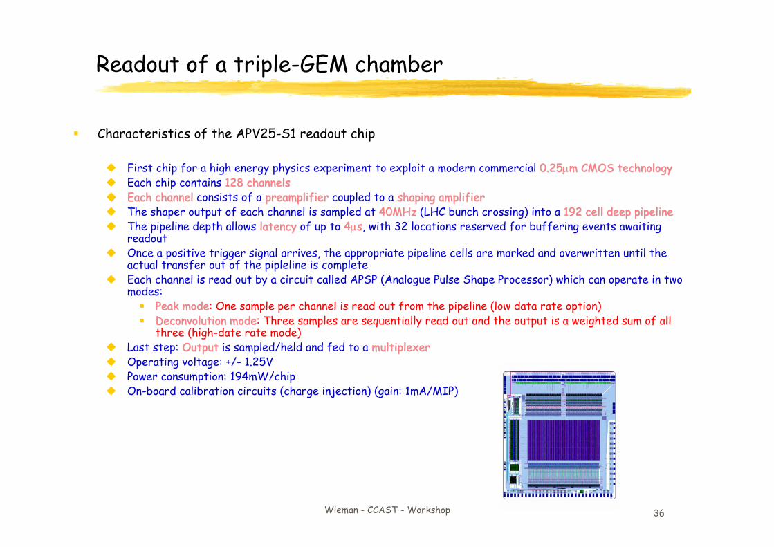
Readout of a triple-GEM chamber
Characteristics of the APV25-S1 readout chip
First chip for a high energy physics experiment to exploit a modern commercial 0.250.25µµm CMOS technologym CMOS technologyEach chip contains 128 channels128 channelsEach channelEach channel consists of a preamplifier preamplifier coupled to a shaping amplifiershaping amplifierThe shaper output of each channel is sampled at 40MHz40MHz (LHC bunch crossing) into a 192 cell deep pipeline192 cell deep pipelineThe pipeline depth allows latencylatency of up to 44µµss, with 32 locations reserved for buffering events awaiting readoutOnce a positive trigger signal arrives, the appropriate pipeline cells are marked and overwritten until the actual transfer out of the pipleline is completeEach channel is read out by a circuit called APSP (Analogue Pulse Shape Processor) which can operate in two modes:
Peak modePeak mode: One sample per channel is read out from the pipeline (low data rate option)Deconvolution modeDeconvolution mode: Three samples are sequentially read out and the output is a weighted sum of all three (high-date rate mode)
Last step: OutputOutput is sampled/held and fed to a multiplexermultiplexerOperating voltage: +/- 1.25VPower consumption: 194mW/chipOn-board calibration circuits (charge injection) (gain: 1mA/MIP)

Wieman - CCAST - Workshop 37
DAQ1000 Developments
J. Landgraf, M. LeVine, T. LjubicicBNL
5000

Wieman - CCAST - Workshop 38
DAQ1000 Architecture

Wieman - CCAST - Workshop 39
The New TPC Receiver Board Design
The fiber link is the ALICE-developed “DDL”2.125 Gbaud optical link (effectively 50 MHz @ 32 bits on LVDS)Bidirectional -will also be used to download pedestals, bad pads etc. to the FEEsWe can reWe can re--use many ALICE components/technologies on the FEE/RDO use many ALICE components/technologies on the FEE/RDO sideside
The Receiver Board is a PCI board (certainly PCI 64/66, probablyPCI-X, hopefully PCI-Express) – plugs in a fast/cheap PC with lots of fast/cheap memory & CPU powerA board exists: ALICE D-RORC
2 X 200 MB/s fiber on a PCI 64/66Available! ($1500+)Available! ($1500+)Fully developed readout software (driver for Linux) the way we (mostly) likeNO cluster-finder in hardware – must be done in software on the PC host (see later)Will be used for the new TOF DAQ (in progress)A modified fiber (GLINK) daughtercard will be used as the new EMC PCI Receiver Board (under deliberation with Rice/TOF engineers)

Wieman - CCAST - Workshop 40
Dual CERN D-RORC with fibers on the board
Pluggable Mezzanine DDL
Single D-RORC with 1 fiber mezzanine (we purchased 4)

Wieman - CCAST - Workshop 41
STAR TPC FEEUpgrade Status6/2004
Fred Bieser

Wieman - CCAST - Workshop 42
Was
Analog store + digitize on FEE cardGather data, serialize, send to DAQ on RDOSubtract pedestals, suppress 0s in DAQ
bottlenecks
analog sampledigitize
sub. pedestalsuppress 0s
serializesend to DAQ
preampshaper

Wieman - CCAST - Workshop 43
Will Be
Preamp/shaper (only) on FEE cardContinuous waveform sampling, digital filtering, & zero suppression in ALTRO chip on RDOFormat, serialize and send to DAQ
on RCU card
digitizeadj. baseline
serializesend to DAQsuppress 0spreamp
shaper

Wieman - CCAST - Workshop 44
ALICE TOPOLOGY

Wieman - CCAST - Workshop 45
STAR TOPOLOGY
32-channel PASA FEE cardsRDO boards with 9 groups of 8 ALTROs acting as 9 ALICE FECswith ‘cable’ interconnectsOne ALICE RCU to control the ALTRO Bus and send data to DAQ via OPTO Link.6 such RDOs per sector just as now.

Wieman - CCAST - Workshop 46
A Forward Meson Spectrometerto Probe Gluon Distributions
FPD participants from UCB/SSL, BNL, Penn State, IHEP Protvino, UCLA, Argonne, TAMU

Wieman - CCAST - Workshop 47
Motivation
Detect D0 -> K0π0 (BR=0.021), or π0π0(0.008)D0 mass = 1864 MeV, π0 = 135 MeV, K0= 498 MeV
Compare π0 and D0 spectra at large xF(>0.3) from pp and dAuqg dominant process
Do light and heavy quarks experience the same energy degradation in traversing the gluon field?Increase acceptance for pp-> π0 X

Wieman - CCAST - Workshop 48
L.Bland
FMS at STAR
~4 tonsMove pump
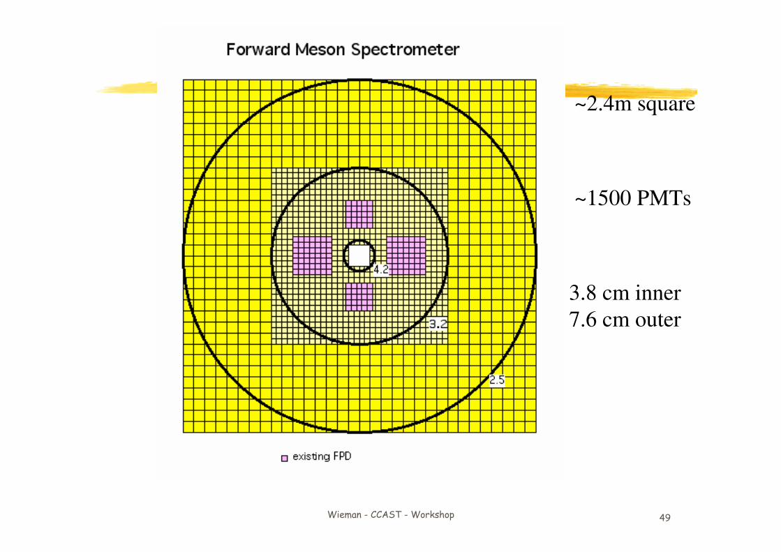
Wieman - CCAST - Workshop 49
~2.4m square
~1500 PMTs
3.8 cm inner7.6 cm outer

Wieman - CCAST - Workshop 50
In summary, STAR upgrade projects:
MRPC TOF Time of FlightHFT Heavy Flavor Tracker – Pixel micro-vertexInner TrackerForward TrackerDAQ1000FEE UpgradeVery Forward Cal

Wieman - CCAST - Workshop 51
Extend PID Capability to higher momentum
Using MRPC

Wieman - CCAST - Workshop 52
Electron Identification
Before, using TPC dE/dx only to separate electrons from hadrons is complicated
TOF detector lights up this study
|1/β-1|<0.03
With TOF PID cut, electron band can be separated from others easily!
A prototype TOF tray (TOFr) installed last year
Wieman - CCAST - Workshop 53

Wieman - CCAST - Workshop 54
Spacious electronic workshop

Wieman - CCAST - Workshop 55
MRPC R&D workshop

Wieman - CCAST - Workshop 56
Outer scene of the workshop
MRPC workshop>200m2
Clean room
Air Shower Room
Assemble room