Embed Size (px)
Citation preview

Page 1 of 17 Version 2.2
CENTER FOR NANOSCALE SCIENCE AND ENGINEERING
Standard Operating Procedures Small Sputtering Machine
Ross Levine
With revisions by: Brian Wajdyk

Page 2 of 17 Version 2.2
Important • Gloves should be worn while handling anything going in vacuum to reduce contamination. • You can only use CeNSE laboratories and equipment if you have been approved by Brian or
Chuck, reserved the tool on the calendar, and filled out a reservation form. No Exceptions! • If the equipment is acting unusual STOP! Place the instrument in the normal standby mode.
Leave a note on the machine. Then please discuss with Brian or Chuck before proceeding. • Any accidental damage must be reported immediately. • All CeNSE laboratories are protected by video surveillance.

Page 3 of 17 Version 2.2
Machine Exterior

Page 4 of 17 Version 2.2
Other Parts of the Machine

Page 5 of 17 Version 2.2
Figure 2d: Chamber lid

Page 6 of 17 Version 2.2
Operating Procedure 1. Preparation
1.1. Before beginning, be sure to wear gloves to reduce contamination and to protect the hands.
2. Load the sample and target 2.1. Open the chamber lid:
2.1.1. Disable the turbo pump by flipping the switch downward on the main panel (figure 1a). Wait about a minute before proceeding.
2.1.2. Disable the rough pump by flipping the switch downward on the main panel (figure 1a). 2.1.3. Look through the chamber window and ensure that the shutter is directly below the gun;
if it is not, the shutter will collide with the chamber wall when opening the lid. 2.1.4. Wait until the chamber is vented. There will be no obvious signs, but the chamber lid will
not open if the chamber is not fully vented. Venting time is typically between 3-5 minutes.
2.1.5. Using a step ladder, unscrew the RF cable (Figure 2d). Place the cable out of the way. 2.1.6. Grab the chamber lid handle and open the chamber lid completely; it will sit upside-
down on its own pole. 2.2. Place the sample on the stage inside the chamber (figure 2b). Ensure that the side on which the
deposition will take place is facing upwards. 2.3. Before placing your target on the gun, check to make sure there is thermal paste on the copper
cathode. The proper amount is thick enough to cover it completely. However it should not be completely opaque.
2.4. Place your target on the gun, with the magnetic keeper facing the gun (figure 2a). 2.5. Close and prepare the chamber:
2.5.1. Close the chamber lid using the handle. The lid is centered over the chamber the lid sticks out all the way around the chamber rim.
2.5.2. Replace the RF cable (Figure 2d). 2.5.3. Turn on the rough pump by flipping the switch upward on the main panel (figure 1a). 2.5.4. After waiting for about 1 minute, turn on the turbo pump by flipping the switch upward.
3. Configure the deposition 3.1. Set the deposition thickness:
3.1.1. Press and hold the thickness button on the deposition monitor (figure 2c). 3.1.2. Use the increase and decrease buttons to set the desired thickness (figure 2c).
3.2. Set the material density: 3.2.1. Use the chart in Appendix A to find the density of the deposition material. 3.2.2. Press and hold the density button on the deposition monitor (figure 2c). 3.2.3. Use the increase and decrease buttons to set the density (figure 2c).
3.3. Set the material’s acoustic impedance: 3.3.1. Use the chart in Appendix A to find the acoustic impedance of the deposition material. 3.3.2. Press and hold the acoustic impedance button on the deposition monitor (figure 2c).
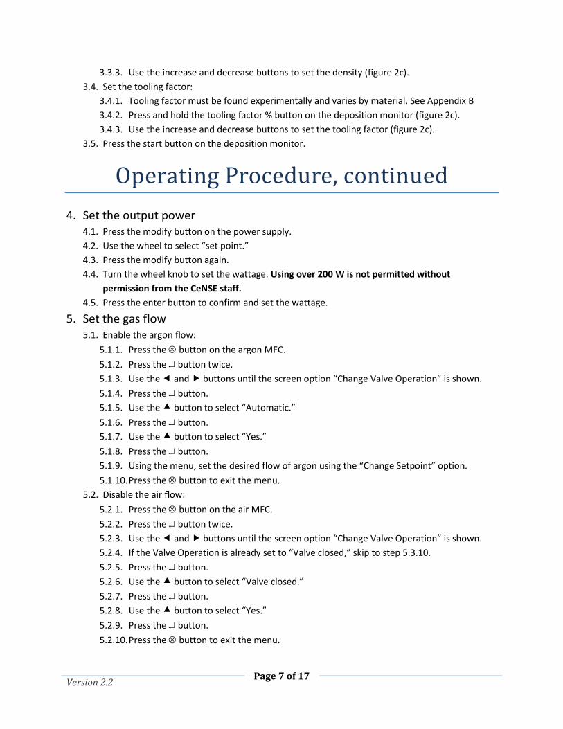
Page 7 of 17 Version 2.2
3.3.3. Use the increase and decrease buttons to set the density (figure 2c). 3.4. Set the tooling factor:
3.4.1. Tooling factor must be found experimentally and varies by material. See Appendix B 3.4.2. Press and hold the tooling factor % button on the deposition monitor (figure 2c). 3.4.3. Use the increase and decrease buttons to set the tooling factor (figure 2c).
3.5. Press the start button on the deposition monitor.
Operating Procedure, continued 4. Set the output power
4.1. Press the modify button on the power supply. 4.2. Use the wheel to select “set point.” 4.3. Press the modify button again. 4.4. Turn the wheel knob to set the wattage. Using over 200 W is not permitted without
permission from the CeNSE staff. 4.5. Press the enter button to confirm and set the wattage.
5. Set the gas flow 5.1. Enable the argon flow:
5.1.1. Press the ⊗ button on the argon MFC. 5.1.2. Press the ↵ button twice. 5.1.3. Use the and buttons until the screen option “Change Valve Operation” is shown. 5.1.4. Press the ↵ button. 5.1.5. Use the button to select “Automatic.” 5.1.6. Press the ↵ button. 5.1.7. Use the button to select “Yes.” 5.1.8. Press the ↵ button. 5.1.9. Using the menu, set the desired flow of argon using the “Change Setpoint” option. 5.1.10. Press the ⊗ button to exit the menu.
5.2. Disable the air flow: 5.2.1. Press the ⊗ button on the air MFC. 5.2.2. Press the ↵ button twice. 5.2.3. Use the and buttons until the screen option “Change Valve Operation” is shown. 5.2.4. If the Valve Operation is already set to “Valve closed,” skip to step 5.3.10. 5.2.5. Press the ↵ button. 5.2.6. Use the button to select “Valve closed.” 5.2.7. Press the ↵ button. 5.2.8. Use the button to select “Yes.” 5.2.9. Press the ↵ button. 5.2.10. Press the ⊗ button to exit the menu.

Page 8 of 17 Version 2.2
Operating Procedure, continued 6. Start the sputtering process
6.1. Ensure that the valve is open on the argon tank. 6.2. Wait until the green light is on. This indicates the turbo pump is at full speed. 6.3. Turn on the “gas” switch. 6.4. Wait for the vacuum to stabilize inside the chamber. 6.5. Turn on the “stage” switch for an isotropic effect. This will to allow the stage to rotate creating
better step coverage and be more conformal to the. When this isn’t desired, such as in a lift-off process, this can be left off.
6.6. Check the RF source display for the letters “IL,” to ensure the interlocks are open. 6.7. Press the “RF” button (Figure 1) to start the plasma. 6.8. Presputter with the shutter closed to remove surface contaminants from the target. 1-2
minutes is usually a good amount of time to presputter. 6.9. When you are ready to begin, turn the shutter fully clockwise open, and quickly press start
again on the deposition monitor to re-zero the measurement. The thickness monitor will automatically turn off the RF power when the desired thickness is reached.
7. End the sputtering process 7.1. Turn off components, in this order:
7.1.1. Turn off the “stage” switch. 7.1.2. Turn off the turbo pump and wait about a minute before proceeding to the next step. 7.1.3. Turn off the rough pump.
7.2. Move the shutter back over the gun. 7.3. Wait for the chamber to pressurize. 7.4. Open the chamber lid as described in steps 2.1.3 through 2.1.5. 7.5. Turn off the gas:
7.5.1. Turn off the “gas” switch. 7.5.2. Close the valve on the argon tank.
7.6. Unload the sample if you are done with it (using gloves). 7.7. If it is no longer needed, remove the target and put it back in its container. If necessary,
carefully use the tool that is attached to the machine to pry it out. Be careful to not scratch the gun.
8. When you are done with the machine 8.1. Close the chamber lid using the handle; ensure the lid is centered over the (empty) chamber. 8.2. Turn on the rough pump by flipping the switch upward. 8.3. Wait about a minute; then turn on the turbo pump by flipping the switch upward.
Page 9 of 17 Version 2.2
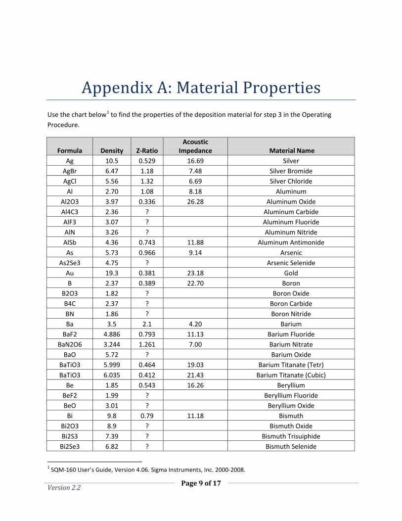
Appendix A: Material Properties Use the chart below1 to find the properties of the deposition material for step 3 in the Operating Procedure.
Formula Density Z-Ratio Acoustic
Impedance Material Name Ag 10.5 0.529 16.69 Silver
AgBr 6.47 1.18 7.48 Silver Bromide AgCl 5.56 1.32 6.69 Silver Chloride
Al 2.70 1.08 8.18 Aluminum Al2O3 3.97 0.336 26.28 Aluminum Oxide Al4C3 2.36 ? Aluminum Carbide AlF3 3.07 ? Aluminum Fluoride AlN 3.26 ? Aluminum Nitride AlSb 4.36 0.743 11.88 Aluminum Antimonide As 5.73 0.966 9.14 Arsenic
As2Se3 4.75 ? Arsenic Selenide Au 19.3 0.381 23.18 Gold B 2.37 0.389 22.70 Boron
B2O3 1.82 ? Boron Oxide B4C 2.37 ? Boron Carbide BN 1.86 ? Boron Nitride Ba 3.5 2.1 4.20 Barium
BaF2 4.886 0.793 11.13 Barium Fluoride BaN2O6 3.244 1.261 7.00 Barium Nitrate
BaO 5.72 ? Barium Oxide BaTiO3 5.999 0.464 19.03 Barium Titanate (Tetr) BaTiO3 6.035 0.412 21.43 Barium Titanate (Cubic)
Be 1.85 0.543 16.26 Beryllium BeF2 1.99 ? Beryllium Fluoride BeO 3.01 ? Beryllium Oxide
Bi 9.8 0.79 11.18 Bismuth Bi2O3 8.9 ? Bismuth Oxide Bi2S3 7.39 ? Bismuth Trisuiphide
Bi2Se3 6.82 ? Bismuth Selenide
1 SQM-160 User’s Guide, Version 4.06. Sigma Instruments, Inc. 2000-2008.

Page 10 of 17 Version 2.2
Formula Density Z-Ratio Acoustic
Impedance Material Name Bi2Te3 7.7 ? Bismuth Telluride
BiF3 5.32 ? Bismuth Fluoride C 2.25 3.26 2.71 Carbon (Graphite) C 3.52 0.22 40.14 Carbon (Diamond)
C8H8 1.1 ? Parlyene (Union Carbide) Ca 1.55 2.62 3.37 Calcium
CaF2 3.18 0.775 11.39 Calcium Fluoride CaO 3.35 ? Calcium Oxide
CaO-SiO2 2.9 ? Calcium Silicate (3) CaSO4 2.962 0.955 9.25 Calcium Sulfate CaTiO3 4.1 ? Calcium Titanate CaWO4 6.06 ? Calcium Tungstate
Cd 8.64 0.682 12.95 Cadmium CdF2 6.64 ? Cadmium Fluoride CdO 8.15 ? Cadmium Oxide CdS 4.83 1.02 8.66 Cadmium Sulfide
CdSe 5.81 ? Cadmium Selenide, CdTe 6.2 0.98 9.01 Cadmium Telluride
Ce 6.78 ? Cerium CeF3 6.16 ? Cerium (III) Fluoride CeO2 7.13 ? Cerium (IV) Dioxide
Co 8.9 0.343 25.74 Cobalt CoO 6.44 0.412 21.43 Cobalt Oxide Cr 7.2 0.305 28.95 Chromium
Cr2O3 5.21 ? Chromium (III) Oxide Cr3C2 6.68 ? Chromium Carbide
CrB 6.17 ? Chromium Boride Cs 1.87 ? Cesium
Cs2SO4 4.243 1.212 7.29 Cesium Sulfate CsBr 4.456 1.41 6.26 Cesium Bromide CsCl 3.988 1.399 6.31 Cesium Chloride CsI 4.516 1.542 5.73 Cesium Iodide Cu 8.93 0.437 20.21 Copper
Cu2O 6 ? Copper Oxide Cu2S Cu2S 5.6 1.58 Copper (I) Sulfide (Alpha) Cu2S Cu2S 5.8 1.52 Copper (I) Sulfide (Beta) CuS CuS 4.6 1.92 Copper (II) Sulfide Dy Dy 8.55 1.03 Dysprosium
Dy2O3 Dy2O3 7.81 1.13 Dysprosium Oxide Er Er 9.05 0.98 Erbium

Page 11 of 17 Version 2.2
Formula Density Z-Ratio Acoustic
Impedance Material Name Er2O3 Er2O3 8.64 1.02 Erbium Oxide
Eu Eu 5.26 1.68 Europium EuF2 EuF2 6.5 1.36 Europium Fluoride
Fe 7.86 0.349 25.30 Iron Fe2O3 5.24 ? Iron Oxide
FeO 5.7 ? Iron Oxide FeS 4.84 ? Iron Sulphide Ga 5.93 0.593 14.89 Gallium
Ga2O3 5.88 ? Gallium Oxide (B) GaAs 5.31 1.59 5.55 Gallium Arsenide GaN 6.1 ? Gallium Nitride GaP 4.1 ? Gallium Phosphide
GaSb 5.6 ? Gallium Antimonide Gd 7.89 0.67 13.18 Gadolinium
Gd2O3 7.41 ? Gadolinium Oxide Ge 5.35 0.516 17.11 Germanium
Ge3N2 5.2 ? Germanium Nitride GeO2 6.24 ? Germanium Oxide GeTe 6.2 ? Germanium Telluride
Hf 13.09 0.36 24.53 Hafnium HfB2 10.5 ? Hafnium Boride, HfC 12.2 ? Hafnium Carbide HfN 13.8 ? Hafnium Nitride
HfO2 9.68 ? Hafnium Oxide HfSi2 7.2 ? Hafnium Silicide
Hg 13.46 0.74 11.93 Mercury Ho 8.8 0.58 15.22 Holminum
Ho2O3 8.41 ? Holminum Oxide In 7.3 0.841 10.50 Indium
In2O3 7.18 ? Indium Sesquioxide In2Se3 5.7 ? Indium Selenide In2Te3 5.8 ? Indium Telluride
InAs 5.7 ? Indium Arsenide InP 4.8 ? Indium Phosphide
InSb 5.76 0.769 11.48 Indium Antimonide Ir 22.4 0.129 68.45 Iridium K 0.86 10.189 0.87 Potassium
KBr 2.75 1.893 4.66 Potassium Bromide KCl 1.98 2.05 4.31 Potassium Chloride KF 2.48 ? Potassium Fluoride

Page 12 of 17 Version 2.2
Formula Density Z-Ratio Acoustic
Impedance Material Name KI 3.128 2.077 4.25 Potassium Iodide La 6.17 0.92 9.60 Lanthanum
La2O3 6.51 ? Lanthanum Oxide LaB6 2.61 ? Lanthanum Boride LaF3 5.94 ? Lanthanum Fluoride
Li 0.53 5.9 1.50 Lithium LiBr 3.47 1.23 7.18 Lithium Bromide LiF 2.638 0.778 11.35 Lithium Fluoride
LiNbO3 4.7 0.463 19.07 Lithium Niobate Lu 9.84 ? Lutetium Mg 1.74 1.61 5.48 Magnesium
MgAl2O4 3.6 ? Magnesium Aluminate MgAl2O6 8 ? Spinel
MgF2 3.18 0.637 13.86 Magnesium Fluoride MgO 3.58 0.411 21.48 Magnesium Oxide Mn 7.2 0.377 23.42 Manganese
MnO 5.39 0.467 18.91 Manganese Oxide MnS 3.99 0.94 9.39 Manganese (II) Sulfide Mo 10.2 0.257 34.36 Molybdenum
Mo2C 9.18 ? Molybdenum Carbide MoB2 7.12 ? Molybdenum Boride MoO3 4.7 ? Molybdenum Trioxdide MoS2 4.8 ? Molybdenum Disulfide
Na 0.97 4.8 1.84 Sodium Na3AlF6 2.9 ? Cryolite
Na5AL3F14 2.9 ? Chiolite NaBr 3.2 ? Sodium Bromide NaCl 2.17 1.57 5.62 Sodium Chloride
NaClO3 2.164 1.565 5.64 Sodium Chlorate NaF 2.558 0.949 9.30 Sodium Fluoride
NaNO3 2.27 1.194 7.40 Sodium Nitrate Nb 8.578 0.492 17.95 Niobium (Columbium)
Nb2O3 7.5 ? Niobium Trioxide Nb2O5 4.47 ? Niobium (V) Oxide NbB2 6.97 ? Niobium Boride NbC 7.82 ? Niobium Carbide NbN 8.4 ? Niobium Nitride Nd 7 ? Neodynium
Nd2O3 7.24 ? Neodynium Oxide NdF3 6.506 ? Neodynium Fluoride

Page 13 of 17 Version 2.2
Formula Density Z-Ratio Acoustic
Impedance Material Name Ni 8.91 0.331 26.68 Nickel
NiCr 8.5 ? Nichrome NiCrFe 8.5 ? Inconel NiFe 8.7 ? Permalloy
NiFeMo 8.9 ? Supermalloy NiO 7.45 ? Nickel Oxide
P3N5 2.51 ? Phosphorus Nitride Pb 11.3 1.13 7.81 Lead
PbCl2 5.85 ? Lead Chloride PbF2 8.24 0.661 13.36 Lead Fluoride PbO 9.53 ? Lead Oxide PbS 7.5 0.566 15.60 Lead Sulfide
PbSe 8.1 ? Lead Selenide PbSnO3 8.1 ? Lead Stannate
PbTe 8.16 0.651 13.56 Lead Telluride Pd 12.038 0.357 24.73 Palladium
PdO 8.31 ? Palladium Oxide Po 9.4 ? Polonium Pr 6.78 ? Praseodymium
Pr2O3 6.88 ? Praseodymium Oxide Pt 21.4 0.245 36.04 Platinum
PtO2 10.2 ? Platinum Oxide Ra 5 ? Radium Rb 1.53 2.54 3.48 Rubidium Rbl 3.55 ? Rubidium Iodide Re 21.04 0.15 58.87 Rhenium Rh 12.41 0.21 42.05 Rhodium Ru 12.362 0.182 48.52 Ruthenium S8 2.07 2.29 3.86 Sulphur Sb 6.62 0.768 11.50 Antimony
Sb2O3 5.2 ? Antimony Trioxide Sb2S3 4.64 ? Antimony Trisulfide
Sc 3 0.91 9.70 Scandium Sc2O3 3.86 ? Scandium Oxide
Se 4.81 0.864 10.22 Selenium Si 2.32 0.712 12.40 Silicon
Si3N4 3.44 *1000 Silicon Nitride SiC 3.22 ? Silicon Carbide SiO 2.13 0.87 10.15 Silicon (II) Oxide
SiO2 2.648 1 8.83 Silicon Dioxide

Page 14 of 17 Version 2.2
Formula Density Z-Ratio Acoustic
Impedance Material Name Sm 7.54 0.89 9.92 Samarium
Sm2O3 7.43 ? Samarium Oxide Sn 7.3 0.724 12.20 Tin
SnO2 6.95 ? Tin Oxide SnS 5.08 ? Tin Sulfide
SnSe 6.18 ? Tin Selenide SnTe 6.44 ? Tin Telluride
Sr 2.6 ? Strontium SrF2 4.277 0.727 12.15 Strontium Fluroide SrO 4.99 0.517 17.08 Strontium Oxide Ta 16.6 0.262 33.70 Tantalum
Ta2O5 8.2 0.3 29.43 Tantalum (V) Oxide TaB2 11.15 ? Tantalum Boride TaC 13.9 ? Tantalum Carbide TaN 16.3 ? Tantalum Nitride Tb 8.27 0.66 13.38 Terbium Tc 11.5 ? Technetium Te 6.25 0.9 9.81 Tellurium
TeO2 5.99 0.862 10.24 Tellurium Oxide Th 11.694 0.484 18.24 Thorium
ThF4 6.32 ? Thorium (IV) Fluoride ThO2 9.86 0.284 31.09 Thorium Dioxide
ThOF2 9.1 ? Thorium Oxyfluoride Ti 4.5 0.628 14.06 Titanium
Ti2O3 4.6 ? Titanium Sesquioxide TiB2 4.5 ? Titanium Boride TiC 4.93 ? Titanium Carbide TiN 5.43 ? Titanium Nitride TiO 4.9 ? Titanium Oxide
TiO2 4.26 0.4 22.08 Titanium (IV) Oxide Tl 11.85 1.55 5.70 Thallium
TlBr 7.56 ? Thallium Bromide TlCl 7 ? Thallium Chloride TlI 7.09 ? Thallium Iodide (B) U 19.05 0.238 37.10 Uranium
U3O8 8.3 ? Tri Uranium Octoxide U4O9 10.969 0.348 25.37 Uranium Oxide UO2 10.97 0.286 30.87 Uranium Dioxide
V 5.96 0.53 16.66 Vanadium V2O5 3.36 ? Vanadium Pentoxide

Page 15 of 17 Version 2.2
Formula Density Z-Ratio Acoustic
Impedance Material Name VB2 5.1 ? Vanadium Boride VC 5.77 ? Vanadium Carbide VN 6.13 ? Vanadium Nitride
VO2 4.34 ? Vanadium Dioxide W 19.3 0.163 54.17 Tungsten
WB2 10.77 ? Tungsten Boride WC 15.6 0.151 58.48 Tungsten Carbide
WO3 7.16 ? Tungsten Trioxide WS2 7.5 ? Tungsten Disulphide WSi2 9.4 ? Tungsten Suicide
Y 4.34 0.835 10.57 Yttrium Y2O3 5.01 ? Yttrium Oxide
Yb 6.98 1.13 7.81 Ytterbium Yb2O3 9.17 ? Ytterbium Oxide
Zn 7.04 0.514 17.18 Zinc Zn3Sb2 6.3 ? Zinc Antimonide
ZnF2 4.95 ? Zinc Fluoride ZnO 5.61 0.556 15.88 Zinc Oxide ZnS 4.09 0.775 11.39 Zinc Sulfide
ZnSe 5.26 0.722 12.23 Zinc Selenide ZnTe 6.34 0.77 11.47 Zinc Telluride
Zr 6.49 0.6 14.72 Zirconium ZrB2 6.08 ? Zirconium Boride ZrC 6.73 0.264 33.45 Zirconium Carbide ZrN 7.09 ? Zirconium Nitride
ZrO2 5.6 ? Zirconium Oxide

Page 16 of 17 Version 2.2
Appendix B: Tooling Factor What is Tooling Factor? Tooling Factor is a correction for the difference in material deposited on the quartz sensor versus the substrate. Illustrated below is an example of how difference in distance between the sensor and substrate causes an incorrect reading as you would see in an electron or thermal evaporation system. It is impossible to place a sensor in exactly the same place as your substrate unless the sensor is your substrate.
How do I determine Tooling Factor?
1. Place your substrate and a sensor in their normal position. Mask part of the substrate with a thin material. Thinner is better (i.e. microscope cover glass).
2. Set Tooling to an approximate value or if unknown use 100. (𝑇𝑜𝑜𝑙𝑖𝑛𝑔𝐴𝑝𝑝𝑟𝑜𝑥𝑖𝑚𝑎𝑡𝑒 ) 3. Set Density and Z-Factor for your material. 4. Deposit 1000Å or more of material. (𝑇ℎ𝑖𝑐𝑘𝑛𝑒𝑠𝑠𝑄𝐶𝑀) 5. Use a profilometer or AFM to measure the substrate’s actual film thickness. (𝑇ℎ𝑖𝑐𝑘𝑛𝑒𝑠𝑠𝐴𝑐𝑡𝑢𝑎𝑙) 6. The Tooling Factor is calculated by:
𝑇𝑜𝑜𝑙𝑖𝑛𝑔𝐴𝑐𝑡𝑢𝑎𝑙 = 𝑇𝑜𝑜𝑙𝑖𝑛𝑔𝐴𝑝𝑝𝑟𝑜𝑥𝑖𝑚𝑎𝑡𝑒 × 𝑇ℎ𝑖𝑐𝑘𝑛𝑒𝑠𝑠𝐴𝑐𝑡𝑢𝑎𝑙 𝑇ℎ𝑖𝑐𝑘𝑛𝑒𝑠𝑠𝑄𝐶𝑀
7. Repeated this procedure a second or third time for increased accuracy.
For example
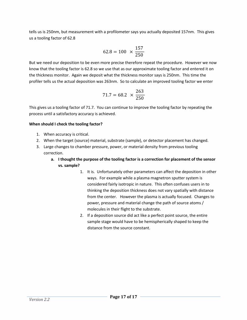
You want to deposit 250nm of Al. We have no idea what a good tooling factor is so we use 100 (which is equivalent to uncorrected) as the approximate tooling factor. We deposit what the thickness monitor
Page 17 of 17 Version 2.2
tells us is 250nm, but measurement with a profilometer says you actually deposited 157nm. This gives us a tooling factor of 62.8
62.8 = 100 × 157 250
But we need our deposition to be even more precise therefore repeat the procedure. However we now know that the tooling factor is 62.8 so we use that as our approximate tooling factor and entered it on the thickness monitor. Again we deposit what the thickness monitor says is 250nm. This time the profiler tells us the actual deposition was 263nm. So to calculate an improved tooling factor we enter
71.7 = 68.2 × 263 250
This gives us a tooling factor of 71.7. You can continue to improve the tooling factor by repeating the process until a satisfactory accuracy is achieved.
When should I check the tooling factor?
1. When accuracy is critical. 2. When the target (source) material, substrate (sample), or detector placement has changed. 3. Large changes to chamber pressure, power, or material density from previous tooling
correction. a. I thought the purpose of the tooling factor is a correction for placement of the sensor
vs. sample? 1. It is. Unfortunately other parameters can affect the deposition in other
ways. For example while a plasma magnetron sputter system is considered fairly isotropic in nature. This often confuses users in to thinking the deposition thickness does not vary spatially with distance from the center. However the plasma is actually focused. Changes to power, pressure and material change the path of source atoms / molecules in their flight to the substrate.
2. If a deposition source did act like a perfect point source, the entire sample stage would have to be hemispherically shaped to keep the distance from the source constant.


![[HH] molecules? Dihalides: A New Stable Ma˜er-Antima˜er … · 2019. 11. 29. · Covalent Bonding in Positron Dihalides: A New Stable Ma˜er-Antima˜er Binding er er Theoretically,](https://img.pdfslide.us/doc/110x75/60daa446b0bf5221cd2aa406/hh-molecules-dihalides-a-new-stable-maoeer-antimaoeer-2019-11-29-covalent.jpg)