Embed Size (px)
Citation preview

Standard Operating Procedure for FEI Helios 660 NanoLab
General Rules
Helios 660 reservations may be made online using the NERCF FOM website. You need a
valid cost object account to charge the reservation if you are an internal UNL user. Please do not
cancel a reservation 24 hours before it starts. Also, please arrive on time for your reservation.
You will be charged at least half an hour of use for late cancellations and missed reservations.
The FOM system will allow other users to start using the Helios 660 if you are late 30 minutes
after your reservation begin.
Users start with daytime access. You may reserve and use the Helios 660 Monday to
Friday 8 a.m. to 5 p.m. Note that daytime access users will not be able to enter the NERCF Lab
and therefore unable to use the Helios 660 during holidays when the UNL offices are closed
despite being able to make reservations on FOM (e.g. MLK Day or winter holidays). Once you
have used the instrument for 50 hours (excluding all trainings or technician-assisted sessions),
you can apply for anytime access. Anytime access users can make reservations anytime and
receive NCard access.
You may use the Helios 660 with other researchers, such as coworkers in your research
group, during daytime hours. However, only trained users can operate the instrument. You are
not allowed to let persons who do not have anytime access to enter the NERCF Lab during off
hours (i.e. weekday nights 5 p.m. to 8 a.m. and weekends).
Please save all data (SEM images, EDS reports, etc.) on the local server – the “D” drive
of the Support Computer. You can retrieve your data by using USB drive with the support
computer or online via email or cloud service. Please do not connect your USB drive to the
Microscope nor EDAX Computers.
If you have questions or technical difficulties while using the Helios 660, please contact
the instrument administrators. Every week, there will be an “office hours” scheduled for users to
seek help.

Special Notes and Warnings
Do not start the instrument if either the red OFF or the yellow STANDBY power
buttons on the front panel is illuminated. Contact the administrator to check if the
instrument is operational.
Always wear the nitrile gloves when touching any part of the chamber.
Always view the CCD chamber camera when opening or closing the sample chamber.
When screwing sample holders onto the stage or sample onto the sample holder, do not
over tighten.
Never use strong force to open the chamber when it is under vacuum. Wait until chamber
is fully vented and the chamber door “pops” open.
Ensure that samples are properly secured to the sample stubs/mounts. Only use the
conductive tape or silver paste that are provided.
Do not use samples that can outgas and/or can generate dust. If you have biological,
archeological, or concrete/cement samples, please check with the instrument
administrators first.
Do not use any ferromagnetic samples with Mode 2 Immersion Mode. These include
alloys with Fe, Ni, Co, and Dy. Even nonmagnetic alloys, such as stainless steel, that
contain these ferromagnetic elements should not be used.
Never insert the EDS, EBSD, CBS, nor STEM detectors when the standard Universal
Mount Base (UMB) or when the Nanoindentor is mounted on the stage.
Always make sure that the chamber has reached high vacuum (i.e. the indicator turns
green) before ending your session and leaving the room.
Be very careful of the electron and ion beam pole pieces. This is a $30,000
replacement if damaged! It is equipped with a touch alarm, which will pop-up as an on-
screen warning if tripped. If you see this, click ok and make sure to reverse whatever
stage movement triggered it, because for the next move the alarm is disabled. Be very
careful.
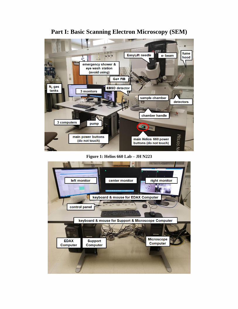
Part I: Basic Scanning Electron Microscopy (SEM)
Figure 1: Helios 660 Lab – JH N223
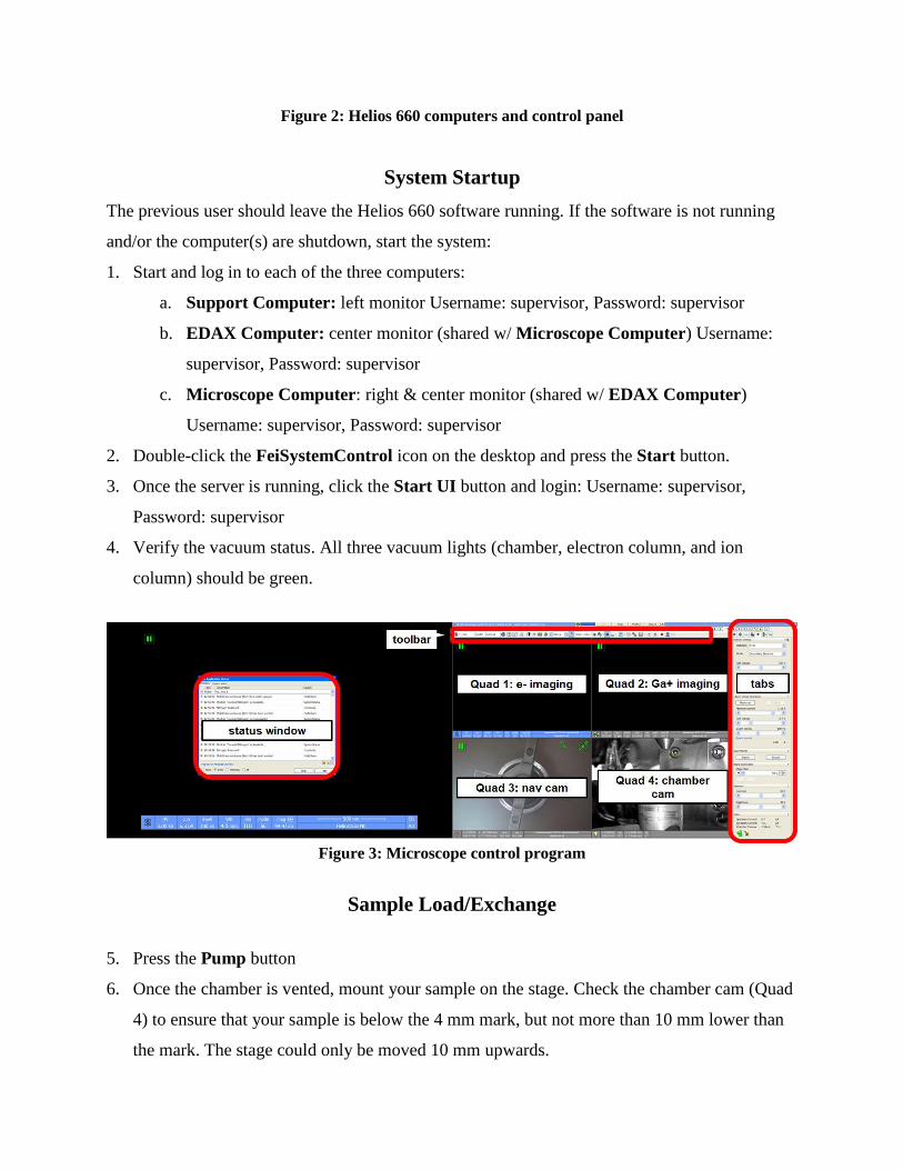
Figure 2: Helios 660 computers and control panel
System Startup
The previous user should leave the Helios 660 software running. If the software is not running
and/or the computer(s) are shutdown, start the system:
1. Start and log in to each of the three computers:
a. Support Computer: left monitor Username: supervisor, Password: supervisor
b. EDAX Computer: center monitor (shared w/ Microscope Computer) Username:
supervisor, Password: supervisor
c. Microscope Computer: right & center monitor (shared w/ EDAX Computer)
Username: supervisor, Password: supervisor
2. Double-click the FeiSystemControl icon on the desktop and press the Start button.
3. Once the server is running, click the Start UI button and login: Username: supervisor,
Password: supervisor
4. Verify the vacuum status. All three vacuum lights (chamber, electron column, and ion
column) should be green.
Figure 3: Microscope control program
Sample Load/Exchange
5. Press the Pump button
6. Once the chamber is vented, mount your sample on the stage. Check the chamber cam (Quad
4) to ensure that your sample is below the 4 mm mark, but not more than 10 mm lower than
the mark. The stage could only be moved 10 mm upwards.

7. If you are loading multiple samples, they must all be within 1mm of the same height to
prevent accidental collisions between the pole pieces and the top of your samples when
imaging.
8. Close the chamber door and press the Pump button. Wait for the chamber vacuum status to
turn green (wait time ~ 3-5 mins).
9. While waiting for vacuum you can take a Nav-cam image by clicking Stage > take Nav-cam
photo. After frame integration is done, double click on the area of your sample you wish to
move the stage to be centered on that location for SEM viewing.
10. Make sure Quad 4 is active, if it’s not, click inside quad 4 and press F6 or the pause button
to have live imaging.
11. Click and drag in the up direction with the mouse wheel to move the stage upward. Bring the
top of your sample to a working distance of about 5 mm (about 1 mm below the yellow line).
Be very careful not to go above the yellow line!
12. When the vacuum indicator for the chamber reaches ~5.5 x 10⁻⁵ torr it will go green, and the
beam controls will become enabled.
13. Turn on the SEM by selecting Quad 1 and hit Beam On under the beam control tab. Only the
SEM will turn on. There is no need to wake up the system.
Keyboard Shortcuts
1. F6: Pauses/activates scanning.
2. F5: Toggles between Quad Screen/Full Screen mode.
3. Ctrl + F5: Toggles between Quad/Full Screen on the middle screen.
4. F9: Starts auto contrast/brightness procedure.
5. Ctrl + F8: displays direct adjustments window.
6. Ctrl + click: Takes an Active Preset Snapshot from all quads with the same beam.
7. Shift + click: Takes a Photo from all quads with the same beam at once.
Be careful when operating the Helios as you may accidentally touch a keyboard shortcut. For full
list of keyboard shortcuts see pages 70-73 of Helios 660 User Manual.
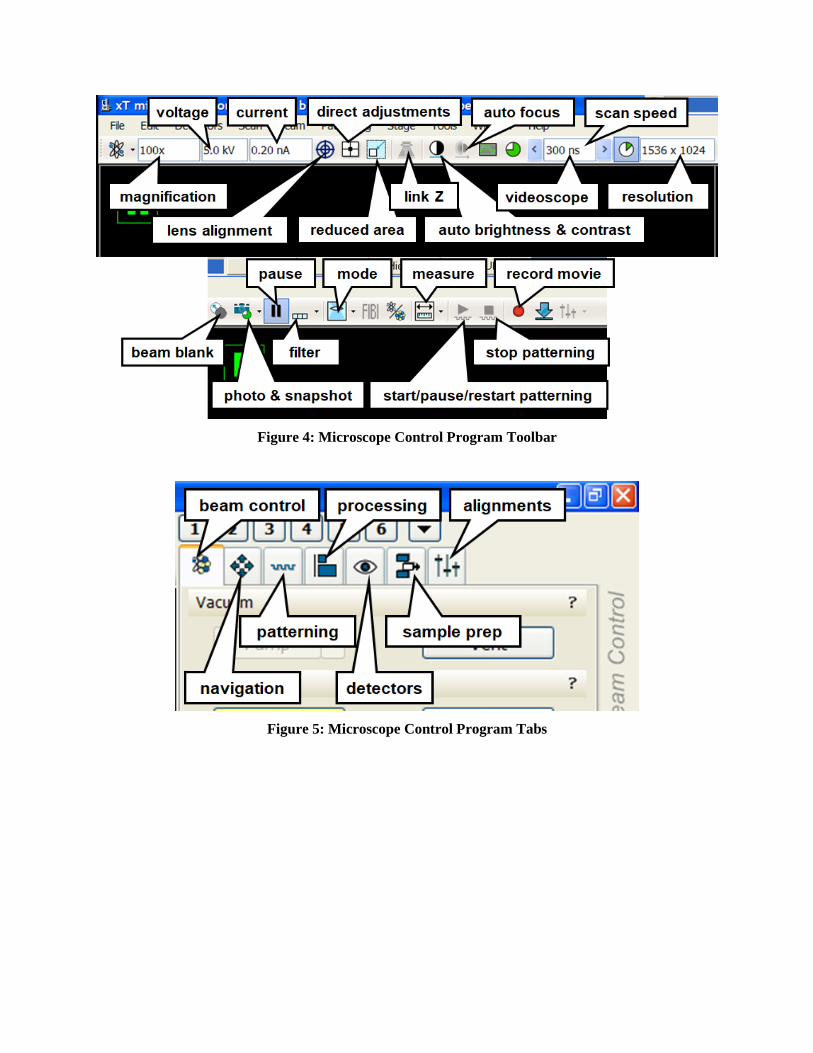
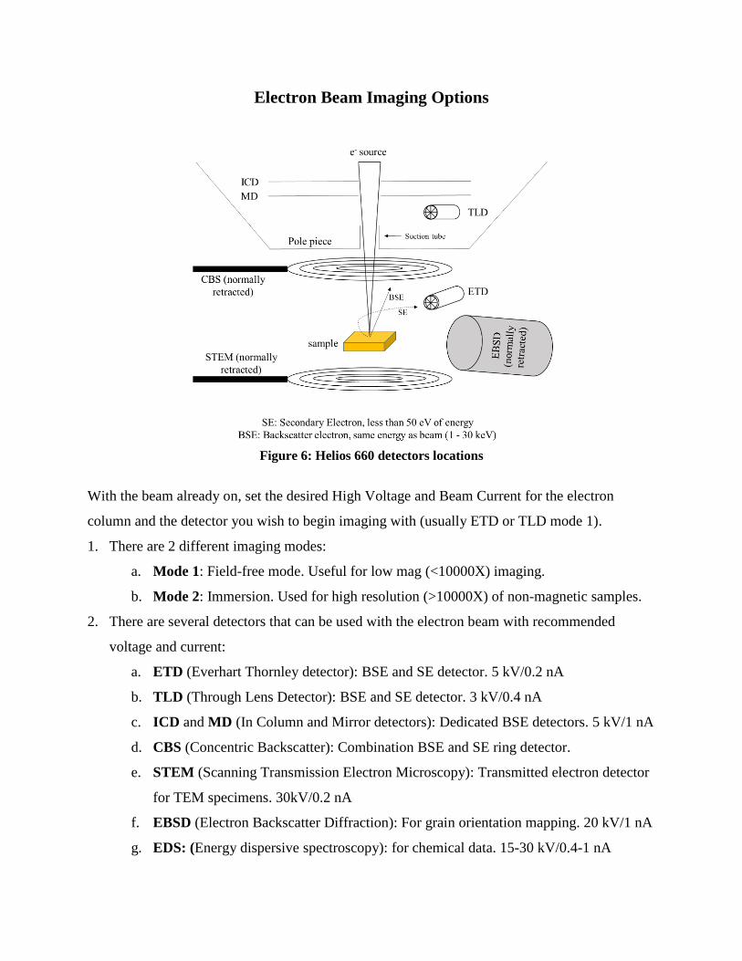
Figure 4: Microscope Control Program Toolbar
Figure 5: Microscope Control Program Tabs
Electron Beam Imaging Options
Figure 6: Helios 660 detectors locations
With the beam already on, set the desired High Voltage and Beam Current for the electron
column and the detector you wish to begin imaging with (usually ETD or TLD mode 1).
1. There are 2 different imaging modes:
a. Mode 1: Field-free mode. Useful for low mag (<10000X) imaging.
b. Mode 2: Immersion. Used for high resolution (>10000X) of non-magnetic samples.
2. There are several detectors that can be used with the electron beam with recommended
voltage and current:
a. ETD (Everhart Thornley detector): BSE and SE detector. 5 kV/0.2 nA
b. TLD (Through Lens Detector): BSE and SE detector. 3 kV/0.4 nA
c. ICD and MD (In Column and Mirror detectors): Dedicated BSE detectors. 5 kV/1 nA
d. CBS (Concentric Backscatter): Combination BSE and SE ring detector.
e. STEM (Scanning Transmission Electron Microscopy): Transmitted electron detector
for TEM specimens. 30kV/0.2 nA
f. EBSD (Electron Backscatter Diffraction): For grain orientation mapping. 20 kV/1 nA
g. EDS: (Energy dispersive spectroscopy): for chemical data. 15-30 kV/0.4-1 nA
*Note: using detectors D-G requires special training.
3. Start image acquisition (F6) in quad 1, and focus on the sample surface (Mag ≈ 1 kX).
4. Couple the Z-axis of the stage to the working distance. Verify the stage position and WD
are the same and accurate.
5. Move the stage upwards to the regular working distance (z = 4 mm).
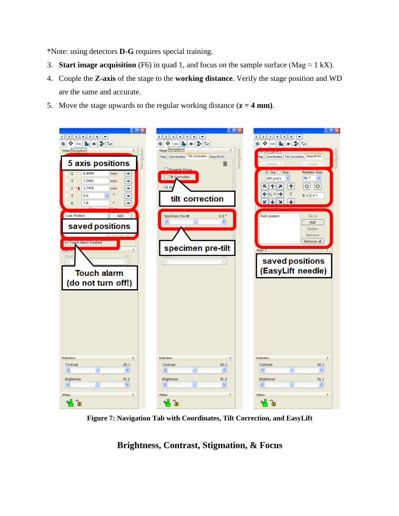
Figure 7: Navigation Tab with Coordinates, Tilt Correction, and EasyLift
Brightness, Contrast, Stigmation, & Focus
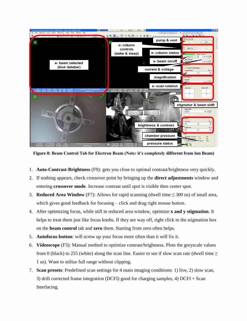
Figure 8: Beam Control Tab for Electron Beam (Note: it’s completely different from Ion Beam)
1. Auto-Contrast-Brightness (F9): gets you close to optimal contrast/brightness very quickly.
2. If nothing appears, check crossover point by bringing up the direct adjustments window and
entering crossover mode. Increase contrast until spot is visible then center spot.
3. Reduced Area Window (F7): Allows for rapid scanning (dwell time ≤ 300 ns) of small area,
which gives good feedback for focusing – click and drag right mouse button.
4. After optimizing focus, while still in reduced area window, optimize x and y stigmation. It
helps to treat them just like focus knobs. If they are way off, right click in the stigmation box
on the beam control tab and zero them. Starting from zero often helps.
5. Autofocus button: will screw up your focus more often than it will fix it.
6. Videoscope (F3): Manual method to optimize contrast/brightness. Plots the greyscale values
from 0 (black) to 255 (white) along the scan line. Easier to see if slow scan rate (dwell time ≥
1 us). Want to utilize full range without clipping.
7. Scan presets: Predefined scan settings for 4 main imaging conditions: 1) live, 2) slow scan,
3) drift corrected frame integration (DCFI) good for charging samples, 4) DCFI + Scan
Interlacing.
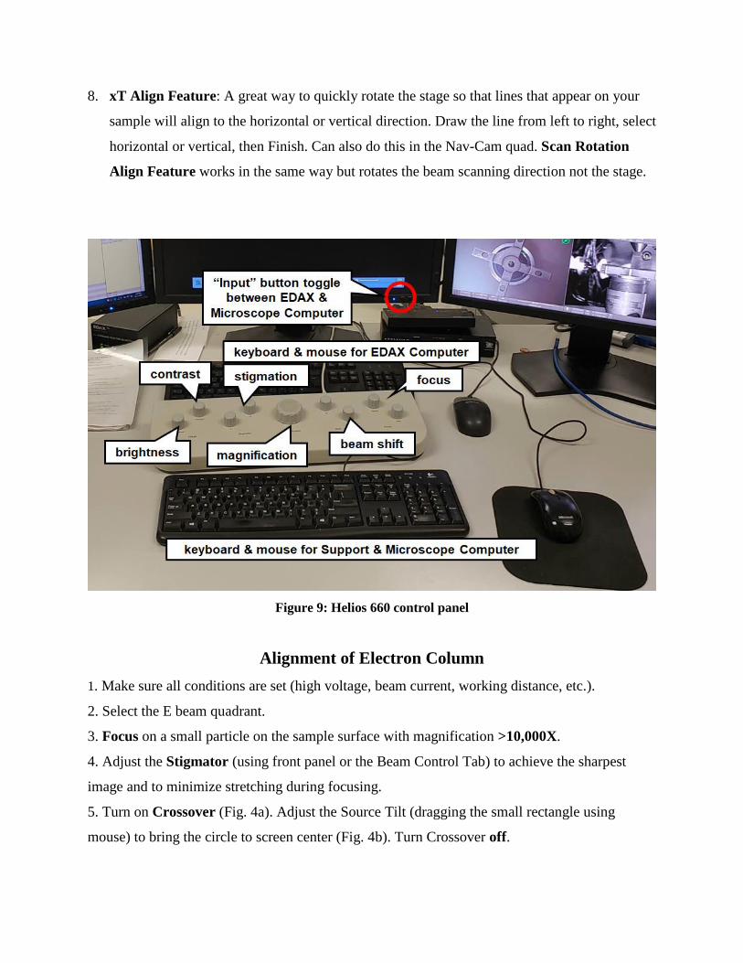
8. xT Align Feature: A great way to quickly rotate the stage so that lines that appear on your
sample will align to the horizontal or vertical direction. Draw the line from left to right, select
horizontal or vertical, then Finish. Can also do this in the Nav-Cam quad. Scan Rotation
Align Feature works in the same way but rotates the beam scanning direction not the stage.
Figure 9: Helios 660 control panel
Alignment of Electron Column
1. Make sure all conditions are set (high voltage, beam current, working distance, etc.).
2. Select the E beam quadrant.
3. Focus on a small particle on the sample surface with magnification >10,000X.
4. Adjust the Stigmator (using front panel or the Beam Control Tab) to achieve the sharpest
image and to minimize stretching during focusing.
5. Turn on Crossover (Fig. 4a). Adjust the Source Tilt (dragging the small rectangle using
mouse) to bring the circle to screen center (Fig. 4b). Turn Crossover off.
6. (Optional) Turn on Lens Align (Fig. 4a). Adjust the Lens Alignment (dragging the small
rectangle using mouse) to minimize translation of the image. Turn Lens Align off.
7. Focus and adjust stigmator again on the small particle. Note: using the reduced window helps
8. Direct Adjustments: Provides further optimization often needed for obtaining high quality
high resolution images. Includes Lens Modulator, Stigmation Centering in X, and Y, which can
be used to further optimize the normal focus and stigmator procedure.
High Resolution Electron Beam Imaging
1. Set desired high voltage and current. 5kV and 43pA is recommended for high resolution
imaging in Immersion mode.
2. In Field-free mode (default mode), go to area of interest, focus sample and correct
stigmation.
3. Make sure the sample is in focus. Link Z to FWD. Read the “Z” value in the Navigation
tab. Lower Z to around 4-5 mm. Focus sample again.
4. Choose Immersion Mode. There are two modes available on the Helios:
a) Mode 1 – Field-free mode, useful for low magnification imaging, imaging during ion milling
and magnetic sample.
b) Mode 2 – Immersion mode, useful for high resolution/high magnification imaging (sample
immersed in lens field, better focusing of e beam, a powerful magnetic field between SEM-
column and sample). For the immersion mode, the minimum magnification is about 1000x and
the working distance usually is around or less than 5mm. A minimum working distance should
be larger than 2 mm.
5. Focus specimen and correct stigmation in Immersion mode.
6. Align Source Tilt and Lens Alignment in Immersion mode. Note: alignment is separate
for the Field-free and Immersion modes. Re-alignment is necessary when switching
modes.
7. Fine Focus, correct stigmation and take high resolution images.
8. When you finish high resolution imaging, return to Field-free mode. Focus and correct
stigmation again. Re-align Source Tilt and Lens Alignment in Field-free Mode.
Note: never load ferromagnetic particles in immersion mode! The strong field can attract
magnetic particles into the pole piece. If a bulk magnetic sample is to be examined in immersion
mode, make sure the sample has been firmly fastened to the stub so that it won’t bump onto the
pole piece by the field!
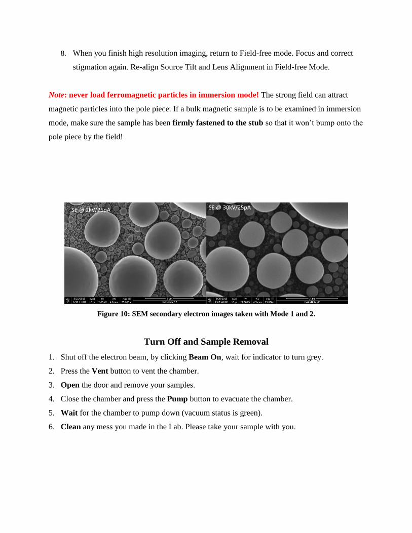
Figure 10: SEM secondary electron images taken with Mode 1 and 2.
Turn Off and Sample Removal
1. Shut off the electron beam, by clicking Beam On, wait for indicator to turn grey.
2. Press the Vent button to vent the chamber.
3. Open the door and remove your samples.
4. Close the chamber and press the Pump button to evacuate the chamber.
5. Wait for the chamber to pump down (vacuum status is green).
6. Clean any mess you made in the Lab. Please take your sample with you.
Part II: Focused Ion Beam (FIB)
Requirements
Part 1 training is required for Part II.
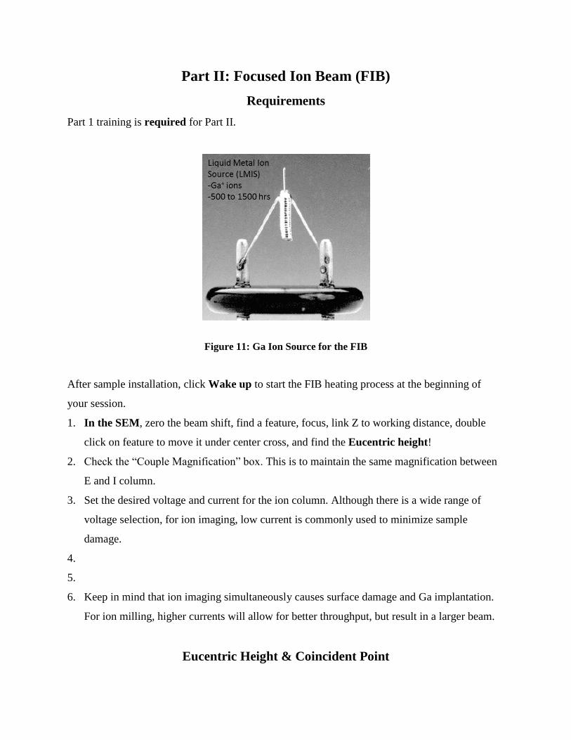
Figure 11: Ga Ion Source for the FIB
After sample installation, click Wake up to start the FIB heating process at the beginning of
your session.
1. In the SEM, zero the beam shift, find a feature, focus, link Z to working distance, double
click on feature to move it under center cross, and find the Eucentric height!
2. Check the “Couple Magnification” box. This is to maintain the same magnification between
E and I column.
3. Set the desired voltage and current for the ion column. Although there is a wide range of
voltage selection, for ion imaging, low current is commonly used to minimize sample
damage.
4.
5.
6. Keep in mind that ion imaging simultaneously causes surface damage and Ga implantation.
For ion milling, higher currents will allow for better throughput, but result in a larger beam.
Eucentric Height & Coincident Point
1. Move the stage (x & y) by holding down the mouse wheel or double clicking the screen.
2. Align a feature on the sample to the center cross on the screen.
3. Tilt the stage to 5 degrees.
4. Adjust the Z-axis of the stage to bring the feature back to the same position. Tilt to 10
degrees, and adjust z again. Tilt back to 0.
5. Tilt to 30 and correct height, and then 52 degrees and correct height. This is eucentric
height: the height at which tilting the stage does not shift the image position in the SEM.
6. Now you are ready to image your sample at tilt angles between 0 – 60 degrees.
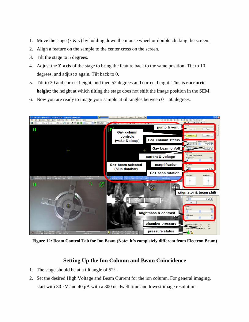
Figure 12: Beam Control Tab for Ion Beam (Note: it’s completely different from Electron Beam)
Setting Up the Ion Column and Beam Coincidence
1. The stage should be at a tilt angle of 52°.
2. Set the desired High Voltage and Beam Current for the ion column. For general imaging,
start with 30 kV and 40 pA with a 300 ns dwell time and lowest image resolution.
3. Run the auto contrast brightness to adjust the ion beam imaging.
4. Take a snapshot with the FIB by activating Quad 2 and pressing the F6 key twice, quickly.
5. The contrast should be ok, but focus/stig might need adjusting. Optimize the focus and
stigmatism between snapshot iterations.
6. Use snapshot imaging setting to minimize beam damage and use camera setting sparsely to
obtain a high quality FIB image.
7. Find the feature you centered in the SEM and use the Beam Shifts to center it in the FIB.
Now the SEM and FIB are looking at the same sample area. This is “Coincidence”. Even if
you change the stage (x, y, tilt, rotate) both beams will remain coincident.
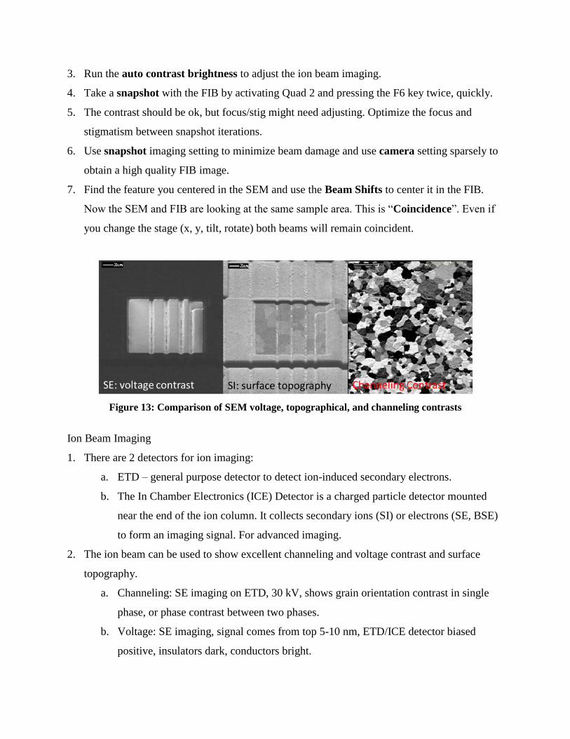
Figure 13: Comparison of SEM voltage, topographical, and channeling contrasts
Ion Beam Imaging
1. There are 2 detectors for ion imaging:
a. ETD – general purpose detector to detect ion-induced secondary electrons.
b. The In Chamber Electronics (ICE) Detector is a charged particle detector mounted
near the end of the ion column. It collects secondary ions (SI) or electrons (SE, BSE)
to form an imaging signal. For advanced imaging.
2. The ion beam can be used to show excellent channeling and voltage contrast and surface
topography.
a. Channeling: SE imaging on ETD, 30 kV, shows grain orientation contrast in single
phase, or phase contrast between two phases.
b. Voltage: SE imaging, signal comes from top 5-10 nm, ETD/ICE detector biased
positive, insulators dark, conductors bright.

c. Surface topography: SI imaging, signal comes from top 5-10 Å, ICE detector biased
negative, shows channeling too, good for imaging oxides.
Milling/Patterning
1. Tabs – located under the scan presets.
2. Select the 3rd tab for patterning. Here you have access to:
a. Predefined patterns (e.g. rectangle, regular xsec, cleaning xsec, line…), and you’ll
notice you can change many of the settings for these patterns under the Basic and
Advanced subtabs. Some of these options are trivial, such as the pattern dimensions
or application, while subtle changes to others can mean the difference between
milling and patterning itself
b. MultiChem Gas Injection Module: Inserts needle that injects metalorganic gases that
destabilize under the beam (SEM or FIB) and deposit one or more component
materials (W, Pt, C, TEOS, H2O).
c. Endpoint Monitor: Provides a way to alternate between milling/patterning in FIB
and monitoring progress with snapshot SEM images (iSPI).
3. Milling speed is a function of beam energy and current. The beam energy controls how
much of the surface is damaged by the beam, and the beam current controls how often these
beam damage events occur, so it changes the rate of milling.
a. Dwell time also affects milling time, longer dwell may help mill through tough
materials
b. Overlap: Each beam current has a different spot size, positive overlap means each
position is adjusted so that these spot sizes overlap each other, which provides an
even milling profile along each scan line and from line to line. 50 % overlap in both x
and y will usually be sufficient.
4. Patterning only works when the right beam conditions are set. Beam energy is usually 30
kV, dwell time should be low (~500 ns), and overlap should be 0 or -0.2. There is a “rule of
thumb” formula for finding the right amount of beam current. First approximate the area of

your pattern in µm2, then multiply that by 5 (Pt), 10 (C), 100 (W), and 3 (TEOS). This
product is a rough estimate of the beam current to use in pA.
a. Ex: To make a 15 µm x 2 µm Pt bar, use (30 µm2) x (5 pA/µm2) = 150 pA.
5. Curtaining occurs when grains mill at different rates, and are generally unavoidable –
especially under Pt protective layers – but can be reduced by lowering the beam current,
increasing overlap or dwell time, and even defocusing the FIB image slightly.
MultiChem operation
1. Deposition can be carried out with either the electron or ion beam. Electron beam induced
deposition will typically provide higher resolution features, but with lower efficiency and
less complete precursor dissociation. Ion beam deposition is more common for most
applications.
2. Etch enhancements (H2O) are designed for use with the ion beam.
3. Before inserting the MultiChem nozzle at either SEM or FIB position, make sure the stage is
at eucentric height. The nozzle is aligned to insert 200 µm above eucentric height. Needless
to say, we don’t want it to crash into your sample!
4. Insert the needle by clicking the appropriate box under the patterning tab.
5. After you have drawn your pattern(s) and set up all parameters, click the play button.
6. It is generally a good idea to wait a bit, pause the pattern, and then take a snapshot of the
pattern and check to make sure it’s working ok before finishing the rest of the pattern.
7. When you are done patterning, retract the MultiChem nozzle.
8. Once retracted, the stage can be moved again.
Shut Down and Sample Removal
7. Set FIB beam current to 3rd lowest preset.
8. Shut off both electron and ion beams.
9. Retract all nozzles, needles, and detectors.
10. Press the Vent button to vent the chamber.
11. When the chamber vents, open the door and remove your samples.
12. Close the chamber and press the Pump button to evacuate the chamber.
13. Wait for the chamber to pump down (vacuum status is green).

14. If you are the last user of the day (check calendar), put the system to Sleep.
15. Clean up any mess you made in the Lab.
Part III: TEM Sample Lift Out Procedure
Requirements
Part 1 and II training are required for Part II.
EasyLift Needle Check & Calibration
1. Before starting, the EasyLift Needle needs to be checked and calibrated.
2. Zero beam shift for both e- and Ga+ beams.
3. Wake Ga+ column and turn on Ga+ beam.
4. Your sample is not required to be installed. However, there needs to be at least something
(i.e. the sample mount) to properly focus the electron beam and set Z height.
5. Click the Alignments tab and select EasyLift Needle Exchange/Calibration program.
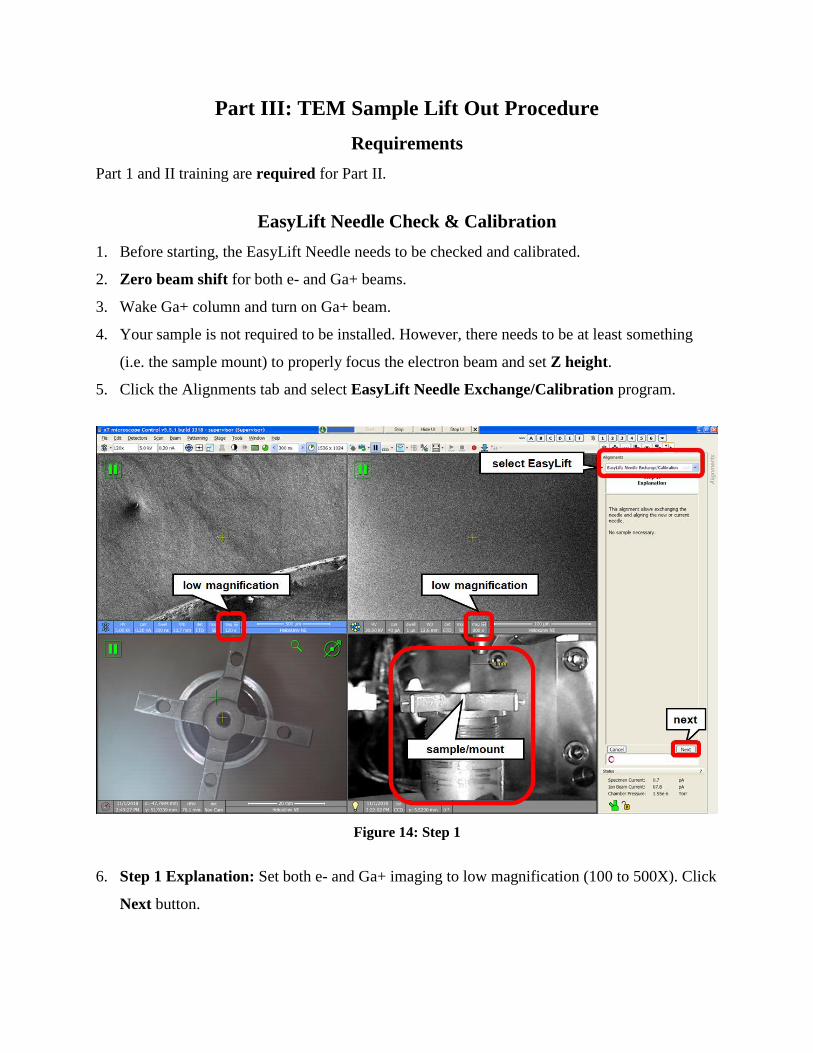
Figure 14: Step 1
6. Step 1 Explanation: Set both e- and Ga+ imaging to low magnification (100 to 500X). Click
Next button.
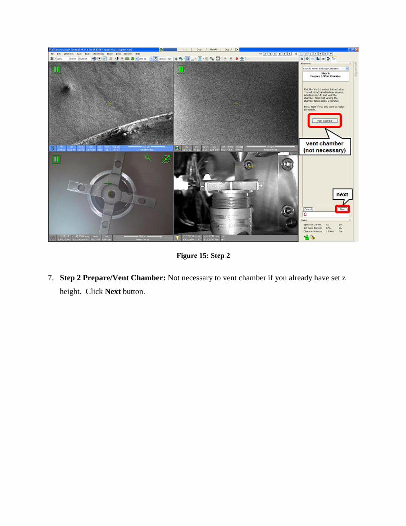
Figure 15: Step 2
7. Step 2 Prepare/Vent Chamber: Not necessary to vent chamber if you already have set z
height. Click Next button.
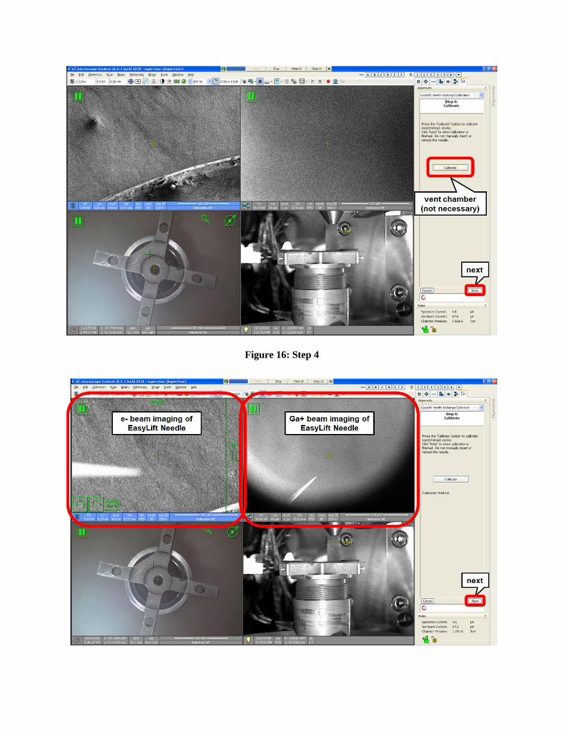
Figure 16: Step 4
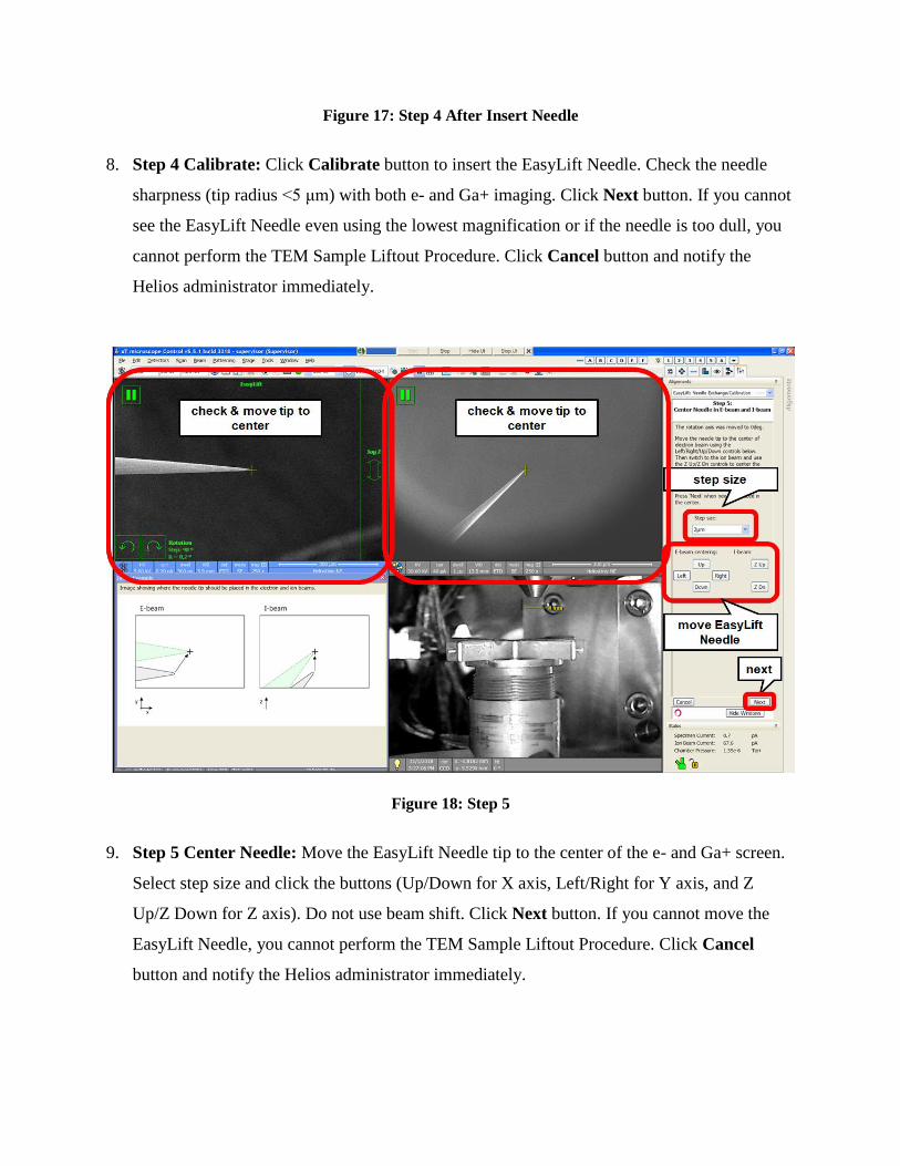
Figure 17: Step 4 After Insert Needle
8. Step 4 Calibrate: Click Calibrate button to insert the EasyLift Needle. Check the needle
sharpness (tip radius <5 μm) with both e- and Ga+ imaging. Click Next button. If you cannot
see the EasyLift Needle even using the lowest magnification or if the needle is too dull, you
cannot perform the TEM Sample Liftout Procedure. Click Cancel button and notify the
Helios administrator immediately.
Figure 18: Step 5
9. Step 5 Center Needle: Move the EasyLift Needle tip to the center of the e- and Ga+ screen.
Select step size and click the buttons (Up/Down for X axis, Left/Right for Y axis, and Z
Up/Z Down for Z axis). Do not use beam shift. Click Next button. If you cannot move the
EasyLift Needle, you cannot perform the TEM Sample Liftout Procedure. Click Cancel
button and notify the Helios administrator immediately.
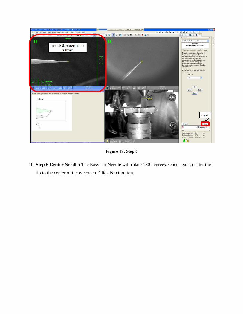
Figure 19: Step 6
10. Step 6 Center Needle: The EasyLift Needle will rotate 180 degrees. Once again, center the
tip to the center of the e- screen. Click Next button.
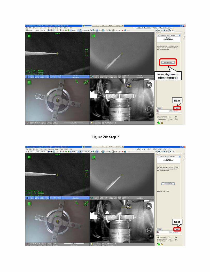
Figure 20: Step 7

Figure 21: Step 7 After Save Alignments
11. Step 7: Click Save Alignment. Click Next button.
Getting Started
1. Use SEM (2 kV, 0.2 nA) to find the area of your sample you want to view in the TEM and
save the stage position under the Navigation tab.
2. Move away from that area, and find a feature to set Eucentric Height and beam coincidence.
3. Increase the beam current to 1.6 nA and focus/stig at a low dwell time.
4. Move back to your region of interest (ROI) without imaging (blind).
E-beam Deposition (Pt or C) Deposition
1. Insert the MultiChem (MC) nozzle.
2. Take a snapshot of your ROI. Change contrast if needed.
3. Select the rectangle tool from the Patterning tab and draw a 10 x 1.5 µm rectangle in the
SEM quad. Mag should be high enough so that the pattern takes up about 1/2 of the image.
4. Hit Play to start patterning. Check after a ~30 seconds to make sure it’s working.
5. When done, retract the MC nozzle and return beam current to 0.2 nA.
2 kV 10 µm x 1.5 µm x 100 nm
1.6 nA 50 % overlap (x and y)
Pt_M_e-dep surface / C_M_e-dep surface 1 µs dwell time
Electron mode Deposition time ~ 5-7 mins
I-beam Deposition (Pt or C, but be consistent with E-Deposition)
1. Tilt the stage to 52˚ (Ctrl-i).
2. Take a snapshot (F6 key x2) with the FIB set at 30 kV and 40 pA. Optimize the
focus/stig/contrast between snapshots (blind). The E-beam deposition should be in the center
of the image if the beams are coincident.
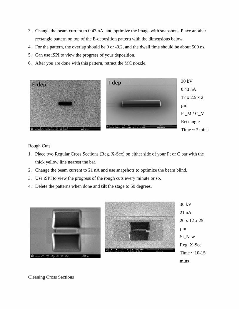
3. Change the beam current to 0.43 nA, and optimize the image with snapshots. Place another
rectangle pattern on top of the E-deposition pattern with the dimensions below.
4. For the pattern, the overlap should be 0 or -0.2, and the dwell time should be about 500 ns.
5. Can use iSPI to view the progress of your deposition.
6. After you are done with this pattern, retract the MC nozzle.
Rough Cuts
1. Place two Regular Cross Sections (Reg. X-Sec) on either side of your Pt or C bar with the
thick yellow line nearest the bar.
2. Change the beam current to 21 nA and use snapshots to optimize the beam blind.
3. Use iSPI to view the progress of the rough cuts every minute or so.
4. Delete the patterns when done and tilt the stage to 50 degrees.
Cleaning Cross Sections
30 kV
0.43 nA
17 x 2.5 x 2
µm
Pt_M / C_M
Rectangle
Time ~ 7 mins
30 kV
21 nA
20 x 12 x 25
µm
Si_New
Reg. X-Sec
Time ~ 10-15
mins
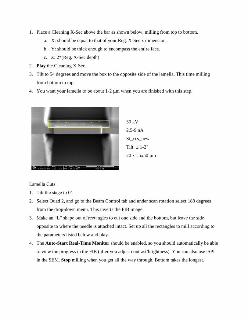
1. Place a Cleaning X-Sec above the bar as shown below, milling from top to bottom.
a. X: should be equal to that of your Reg. X-Sec x dimension.
b. Y: should be thick enough to encompass the entire face.
c. Z: 2*(Reg. X-Sec depth)
2. Play the Cleaning X-Sec.
3. Tilt to 54 degrees and move the box to the opposite side of the lamella. This time milling
from bottom to top.
4. You want your lamella to be about 1-2 µm when you are finished with this step.
Lamella Cuts
1. Tilt the stage to 0˚.
2. Select Quad 2, and go to the Beam Control tab and under scan rotation select 180 degrees
from the drop-down menu. This inverts the FIB image.
3. Make an “L” shape out of rectangles to cut one side and the bottom, but leave the side
opposite to where the needle is attached intact. Set up all the rectangles to mill according to
the parameters listed below and play.
4. The Auto-Start Real-Time Monitor should be enabled, so you should automatically be able
to view the progress in the FIB (after you adjust contrast/brightness). You can also use iSPI
in the SEM. Stop milling when you get all the way through. Bottom takes the longest.
30 kV
2.5-9 nA
Si_ccs_new
Tilt: ± 1-2˚
20 x1.5x50 µm
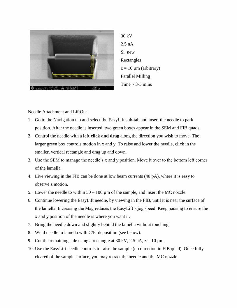
Needle Attachment and LiftOut
1. Go to the Navigation tab and select the EasyLift sub-tab and insert the needle to park
position. After the needle is inserted, two green boxes appear in the SEM and FIB quads.
2. Control the needle with a left click and drag along the direction you wish to move. The
larger green box controls motion in x and y. To raise and lower the needle, click in the
smaller, vertical rectangle and drag up and down.
3. Use the SEM to manage the needle’s x and y position. Move it over to the bottom left corner
of the lamella.
4. Live viewing in the FIB can be done at low beam currents (40 pA), where it is easy to
observe z motion.
5. Lower the needle to within 50 – 100 µm of the sample, and insert the MC nozzle.
6. Continue lowering the EasyLift needle, by viewing in the FIB, until it is near the surface of
the lamella. Increasing the Mag reduces the EasyLift’s jog speed. Keep pausing to ensure the
x and y position of the needle is where you want it.
7. Bring the needle down and slightly behind the lamella without touching.
8. Weld needle to lamella with C/Pt deposition (see below).
9. Cut the remaining side using a rectangle at 30 kV, 2.5 nA, z = 10 µm.
10. Use the EasyLift needle controls to raise the sample (up direction in FIB quad). Once fully
cleared of the sample surface, you may retract the needle and the MC nozzle.
30 kV
2.5 nA
Si_new
Rectangles
z = 10 µm (arbitrary)
Parallel Milling
Time ~ 3-5 mins
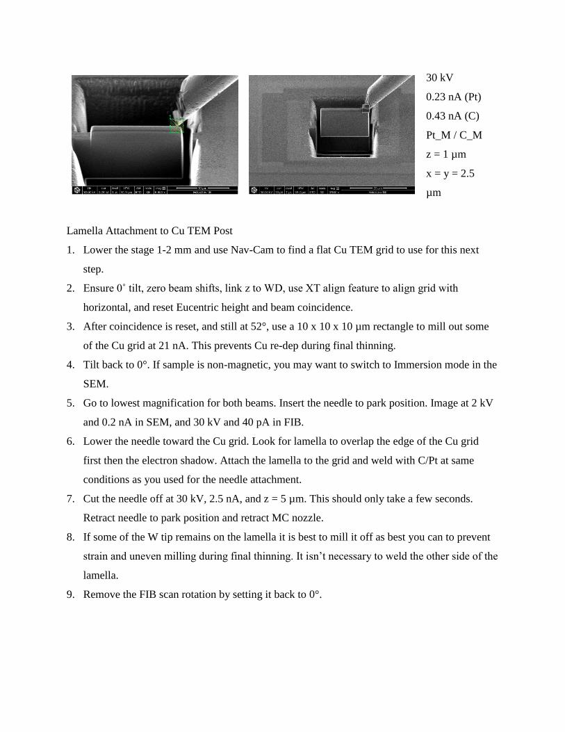
Lamella Attachment to Cu TEM Post
1. Lower the stage 1-2 mm and use Nav-Cam to find a flat Cu TEM grid to use for this next
step.
2. Ensure 0˚ tilt, zero beam shifts, link z to WD, use XT align feature to align grid with
horizontal, and reset Eucentric height and beam coincidence.
3. After coincidence is reset, and still at 52°, use a 10 x 10 x 10 µm rectangle to mill out some
of the Cu grid at 21 nA. This prevents Cu re-dep during final thinning.
4. Tilt back to 0°. If sample is non-magnetic, you may want to switch to Immersion mode in the
SEM.
5. Go to lowest magnification for both beams. Insert the needle to park position. Image at 2 kV
and 0.2 nA in SEM, and 30 kV and 40 pA in FIB.
6. Lower the needle toward the Cu grid. Look for lamella to overlap the edge of the Cu grid
first then the electron shadow. Attach the lamella to the grid and weld with C/Pt at same
conditions as you used for the needle attachment.
7. Cut the needle off at 30 kV, 2.5 nA, and z = 5 µm. This should only take a few seconds.
Retract needle to park position and retract MC nozzle.
8. If some of the W tip remains on the lamella it is best to mill it off as best you can to prevent
strain and uneven milling during final thinning. It isn’t necessary to weld the other side of the
lamella.
9. Remove the FIB scan rotation by setting it back to 0°.
30 kV
0.23 nA (Pt)
0.43 nA (C)
Pt_M / C_M
z = 1 µm
x = y = 2.5
µm
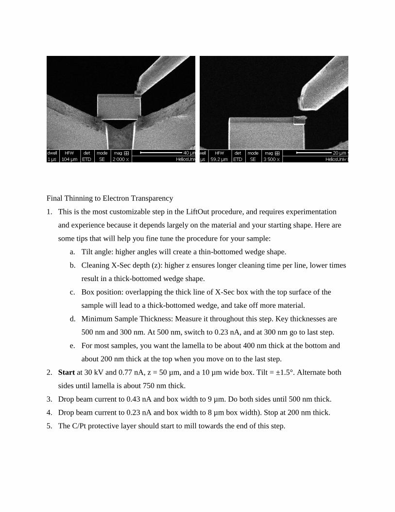
Final Thinning to Electron Transparency
1. This is the most customizable step in the LiftOut procedure, and requires experimentation
and experience because it depends largely on the material and your starting shape. Here are
some tips that will help you fine tune the procedure for your sample:
a. Tilt angle: higher angles will create a thin-bottomed wedge shape.
b. Cleaning X-Sec depth (z): higher z ensures longer cleaning time per line, lower times
result in a thick-bottomed wedge shape.
c. Box position: overlapping the thick line of X-Sec box with the top surface of the
sample will lead to a thick-bottomed wedge, and take off more material.
d. Minimum Sample Thickness: Measure it throughout this step. Key thicknesses are
500 nm and 300 nm. At 500 nm, switch to 0.23 nA, and at 300 nm go to last step.
e. For most samples, you want the lamella to be about 400 nm thick at the bottom and
about 200 nm thick at the top when you move on to the last step.
2. Start at 30 kV and 0.77 nA, z = 50 µm, and a 10 µm wide box. Tilt = ±1.5°. Alternate both
sides until lamella is about 750 nm thick.
3. Drop beam current to 0.43 nA and box width to 9 µm. Do both sides until 500 nm thick.
4. Drop beam current to 0.23 nA and box width to 8 µm box width). Stop at 200 nm thick.
5. The C/Pt protective layer should start to mill towards the end of this step.
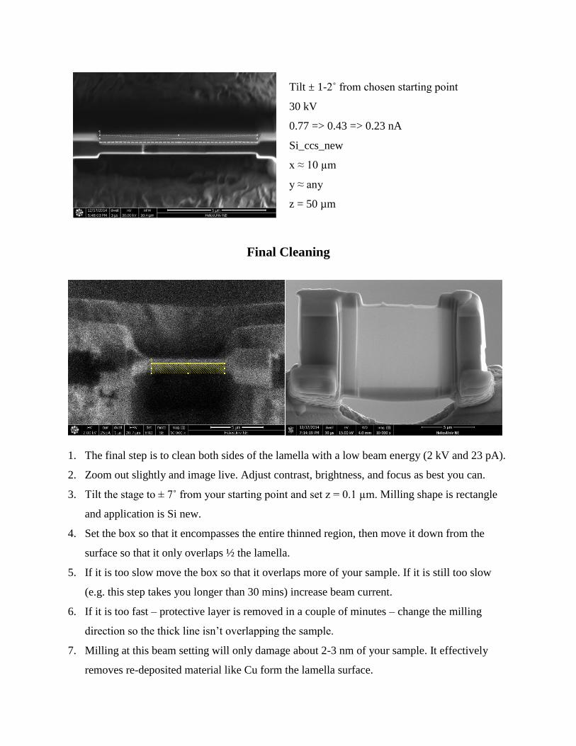
Final Cleaning
1. The final step is to clean both sides of the lamella with a low beam energy (2 kV and 23 pA).
2. Zoom out slightly and image live. Adjust contrast, brightness, and focus as best you can.
3. Tilt the stage to ± 7˚ from your starting point and set z = 0.1 µm. Milling shape is rectangle
and application is Si new.
4. Set the box so that it encompasses the entire thinned region, then move it down from the
surface so that it only overlaps ½ the lamella.
5. If it is too slow move the box so that it overlaps more of your sample. If it is still too slow
(e.g. this step takes you longer than 30 mins) increase beam current.
6. If it is too fast – protective layer is removed in a couple of minutes – change the milling
direction so the thick line isn’t overlapping the sample.
7. Milling at this beam setting will only damage about 2-3 nm of your sample. It effectively
removes re-deposited material like Cu form the lamella surface.
Tilt ± 1-2˚ from chosen starting point
30 kV
0.77 => 0.43 => 0.23 nA
Si_ccs_new
x ≈ 10 µm
y ≈ any
z = 50 µm

8. Each side should take about 5-10 mins.
9. View the top surface at high mag (immersion mode) using iSPI every 15 seconds.
10. Stop when only a few 100 nm of C/Pt are left on the lamella. Watch the protective layer
constantly during this step to see how much is being removed by each scan.
Part IV: EDS Version
Requirements
Part 1 training is required for Part II.
The “EDAX” system mounted on our Helios is an X-Ray analysis system capable of producing
an energy spectrum from X-Rays emanating from a specimen material that is struck by energetic
electrons and analyzing the data to determine what elements are producing the X-rays. This
principle is termed Energy Dispersive (X-ray) Spectroscopy (EDS).
Step 1, Check SEM parameters, Select an appropriate electron acceleration voltage for your
material (normally 10 kV - 30 kV) by checking the K, L, and/or M characteristic X-rays of your
elements of interest.
Step 2, Log in to EDAX TEAM User ID: Administrator Password: apollo
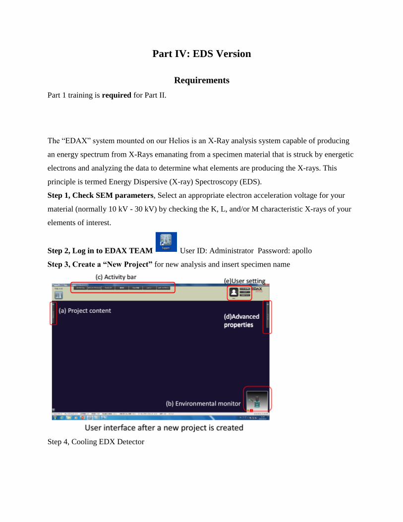
Step 3, Create a “New Project” for new analysis and insert specimen name
Step 4, Cooling EDX Detector
Cooling down EDX detector is compulsory before analysis. (1) Click the [Advanced Property]→
the [EDS detectors]→ the [Det1- Detector Status]; (2) Click the red[Cooling off] button; (3)
Wait until the indication becomes the green, which will take about 2 mins.
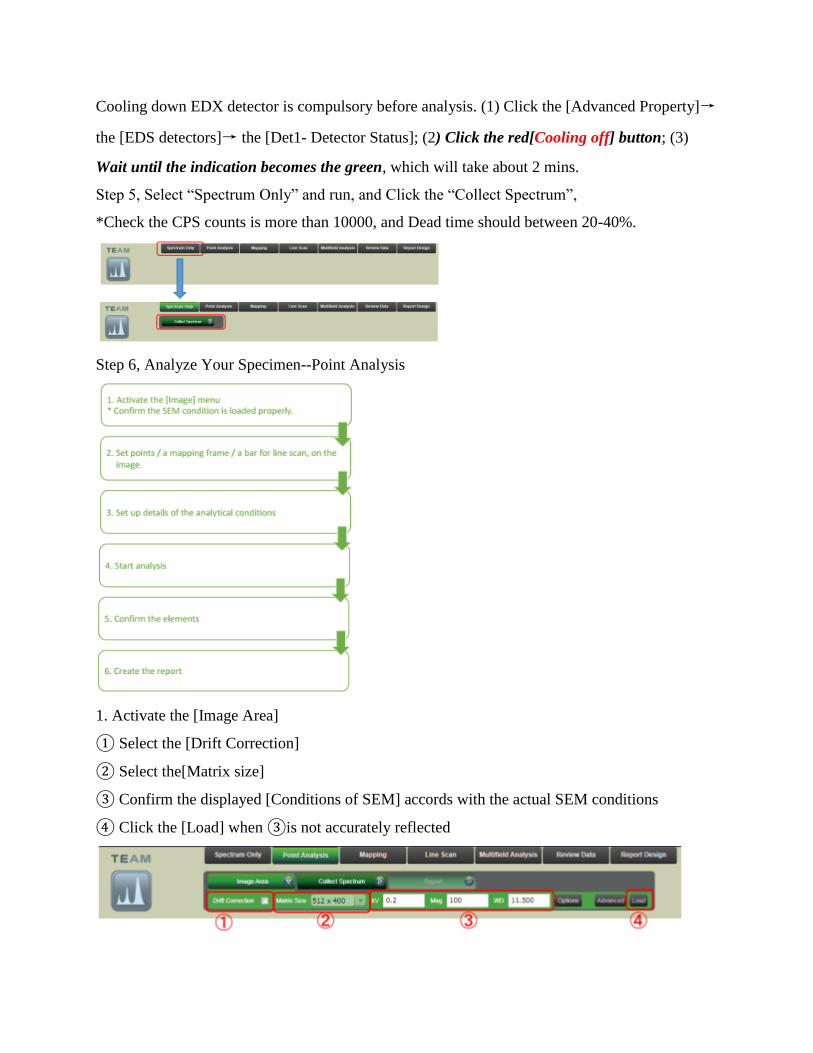
Step 5, Select “Spectrum Only” and run, and Click the “Collect Spectrum”,
*Check the CPS counts is more than 10000, and Dead time should between 20-40%.
Step 6, Analyze Your Specimen--Point Analysis
1. Activate the [Image Area]
① Select the [Drift Correction]
② Select the[Matrix size]
③ Confirm the displayed [Conditions of SEM] accords with the actual SEM conditions
④ Click the [Load] when ③is not accurately reflected
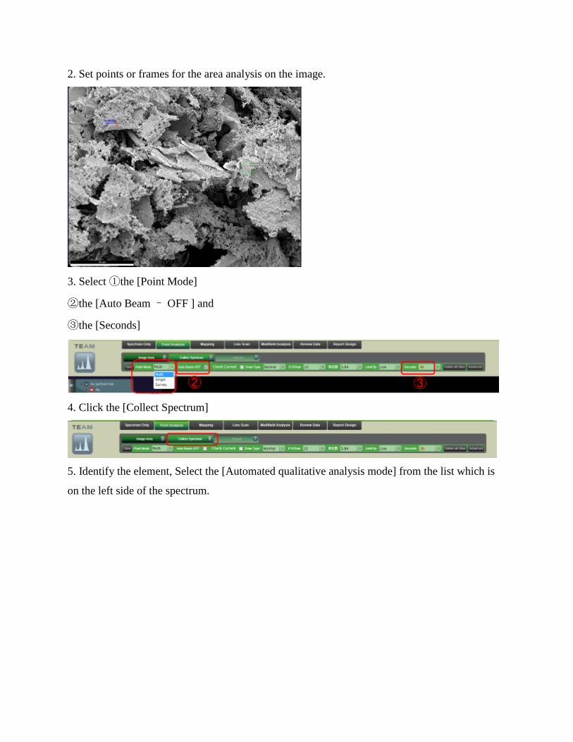
2. Set points or frames for the area analysis on the image.
3. Select ①the [Point Mode]
②the [Auto Beam – OFF ] and
③the [Seconds]
4. Click the [Collect Spectrum]
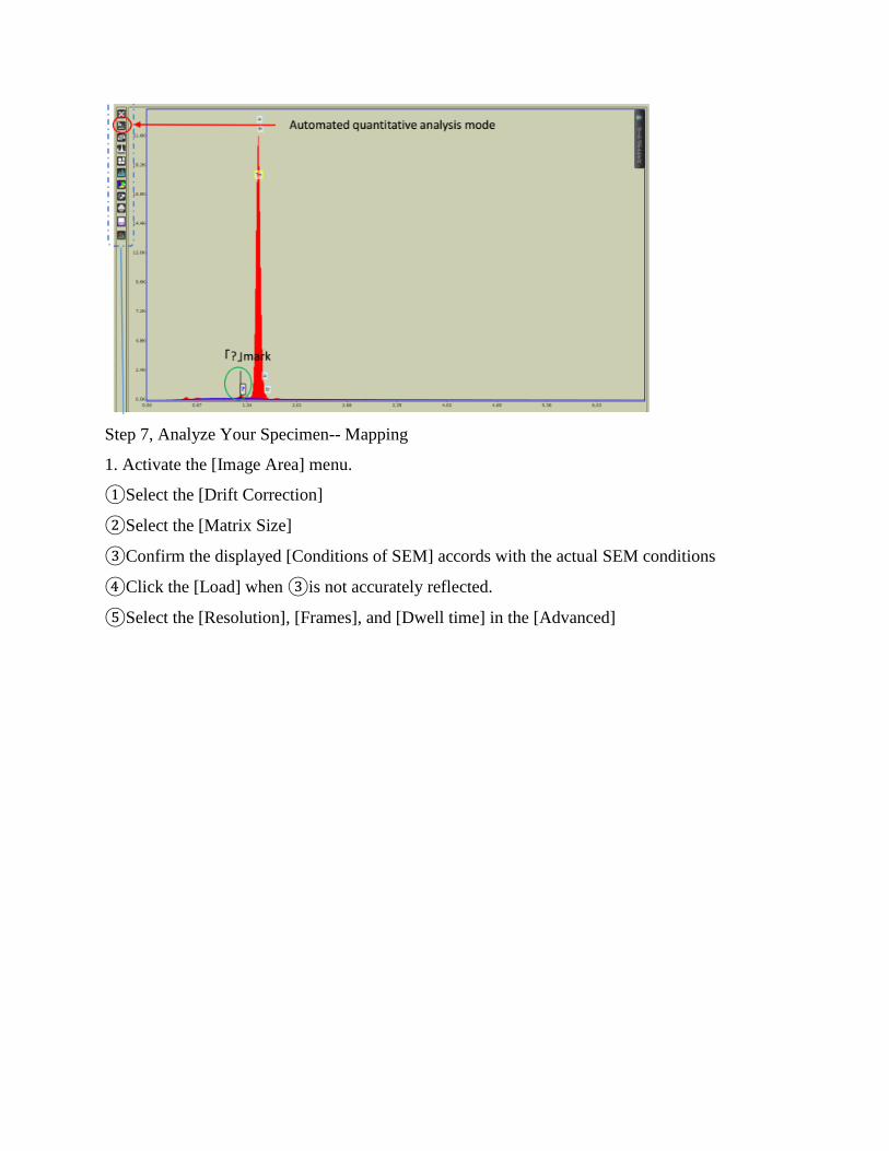
5. Identify the element, Select the [Automated qualitative analysis mode] from the list which is
on the left side of the spectrum.
Step 7, Analyze Your Specimen-- Mapping
1. Activate the [Image Area] menu.
①Select the [Drift Correction]
②Select the [Matrix Size]
③Confirm the displayed [Conditions of SEM] accords with the actual SEM conditions
④Click the [Load] when ③is not accurately reflected.
⑤Select the [Resolution], [Frames], and [Dwell time] in the [Advanced]
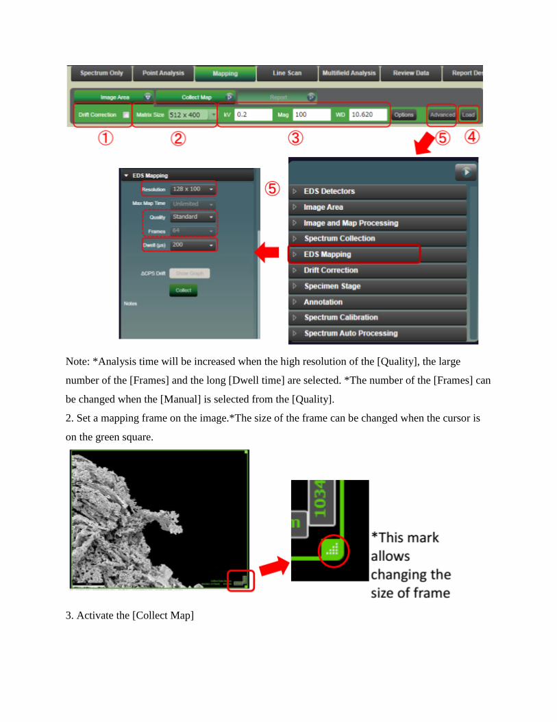
Note: *Analysis time will be increased when the high resolution of the [Quality], the large
number of the [Frames] and the long [Dwell time] are selected. *The number of the [Frames] can
be changed when the [Manual] is selected from the [Quality].
2. Set a mapping frame on the image.*The size of the frame can be changed when the cursor is
on the green square.
3. Activate the [Collect Map]
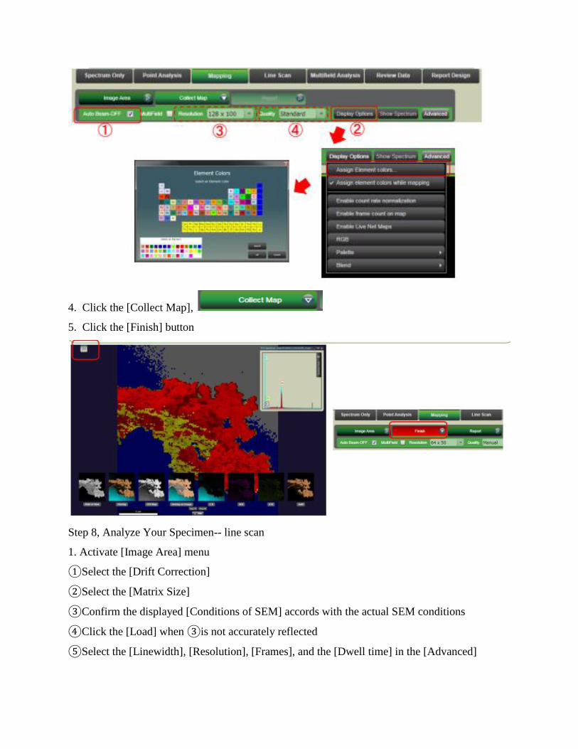
4. Click the [Collect Map],
5. Click the [Finish] button
Step 8, Analyze Your Specimen-- line scan
1. Activate [Image Area] menu
①Select the [Drift Correction]
②Select the [Matrix Size]
③Confirm the displayed [Conditions of SEM] accords with the actual SEM conditions
④Click the [Load] when ③is not accurately reflected
⑤Select the [Linewidth], [Resolution], [Frames], and the [Dwell time] in the [Advanced]
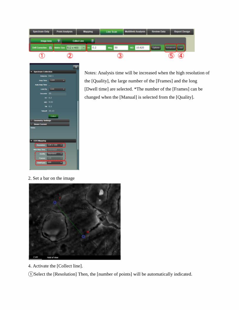
Notes: Analysis time will be increased when the high resolution of
the [Quality], the large number of the [Frames] and the long
[Dwell time] are selected. *The number of the [Frames] can be
changed when the [Manual] is selected from the [Quality].
2. Set a bar on the image
4. Activate the [Collect line].
①Select the [Resolution] Then, the [number of points] will be automatically indicated.
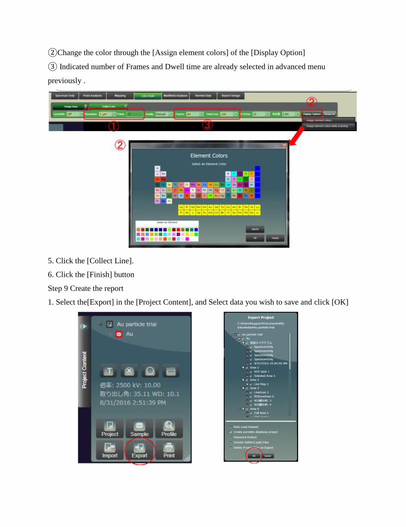
②Change the color through the [Assign element colors] of the [Display Option]
③ Indicated number of Frames and Dwell time are already selected in advanced menu
previously .
5. Click the [Collect Line].
6. Click the [Finish] button
Step 9 Create the report
1. Select the[Export] in the [Project Content], and Select data you wish to save and click [OK]
3. Save the [ZIP file] as the raw data
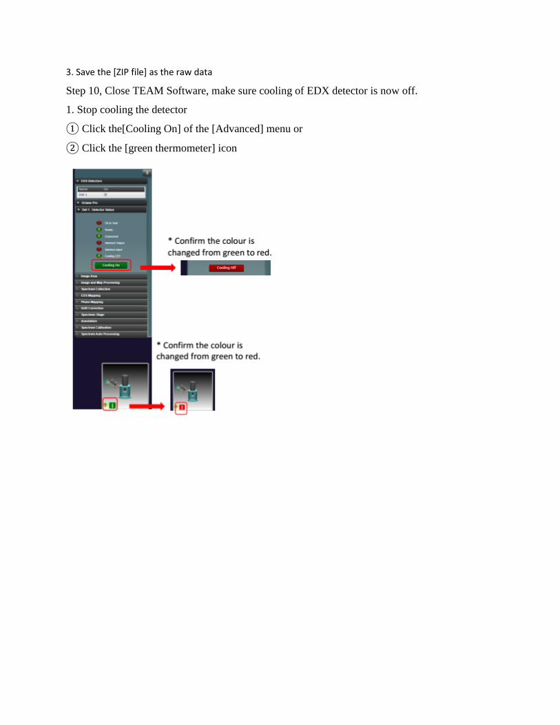
Step 10, Close TEAM Software, make sure cooling of EDX detector is now off.
1. Stop cooling the detector
① Click the[Cooling On] of the [Advanced] menu or
② Click the [green thermometer] icon
Part V: EBSD Operation Manual
Requirements
Part 1 training is required for Part V.
Sample Set-up
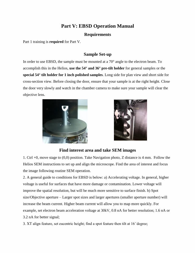
In order to use EBSD, the sample must be mounted at a 70° angle to the electron beam. To
accomplish this in the Helios, use the 54° and 36° pre-tilt holder for general samples or the
special 54° tilt holder for 1 inch polished samples. Long side for plan view and short side for
cross-section view. Before closing the door, ensure that your sample is at the right height. Close
the door very slowly and watch in the chamber camera to make sure your sample will clear the
objective lens.
Find interest area and take SEM images
1. Ctrl +0, move stage to (0,0) position. Take Navigation photo, Z distance is 4 mm. Follow the
Helios SEM instructions to set up and align the microscope. Find the area of interest and focus
the image following routine SEM operation.
2. A general guide to conditions for EBSD is below: a) Accelerating voltage. In general, higher
voltage is useful for surfaces that have more damage or contamination. Lower voltage will
improve the spatial resolution, but will be much more sensitive to surface finish. b) Spot
size/Objective aperture – Larger spot sizes and larger apertures (smaller aperture number) will
increase the beam current. Higher beam current will allow you to map more quickly. For
example, set electron beam acceleration voltage at 30kV, 0.8 nA for better resolution; 1.6 nA or
3.2 nA for better signal;
3. XT align feature, set eucentric height; find a spot feature then tilt at 16 ̊ degree;
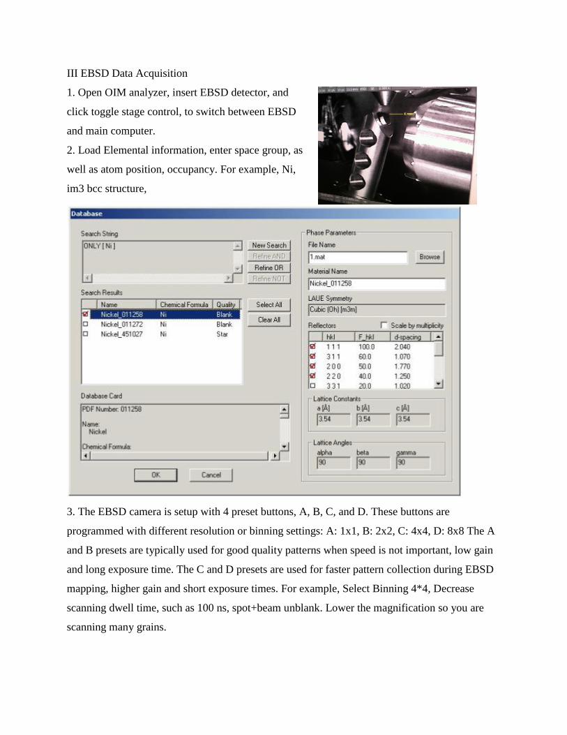
III EBSD Data Acquisition
1. Open OIM analyzer, insert EBSD detector, and
click toggle stage control, to switch between EBSD
and main computer.
2. Load Elemental information, enter space group, as
well as atom position, occupancy. For example, Ni,
im3 bcc structure,
3. The EBSD camera is setup with 4 preset buttons, A, B, C, and D. These buttons are
programmed with different resolution or binning settings: A: 1x1, B: 2x2, C: 4x4, D: 8x8 The A
and B presets are typically used for good quality patterns when speed is not important, low gain
and long exposure time. The C and D presets are used for faster pattern collection during EBSD
mapping, higher gain and short exposure times. For example, Select Binning 4*4, Decrease
scanning dwell time, such as 100 ns, spot+beam unblank. Lower the magnification so you are
scanning many grains.
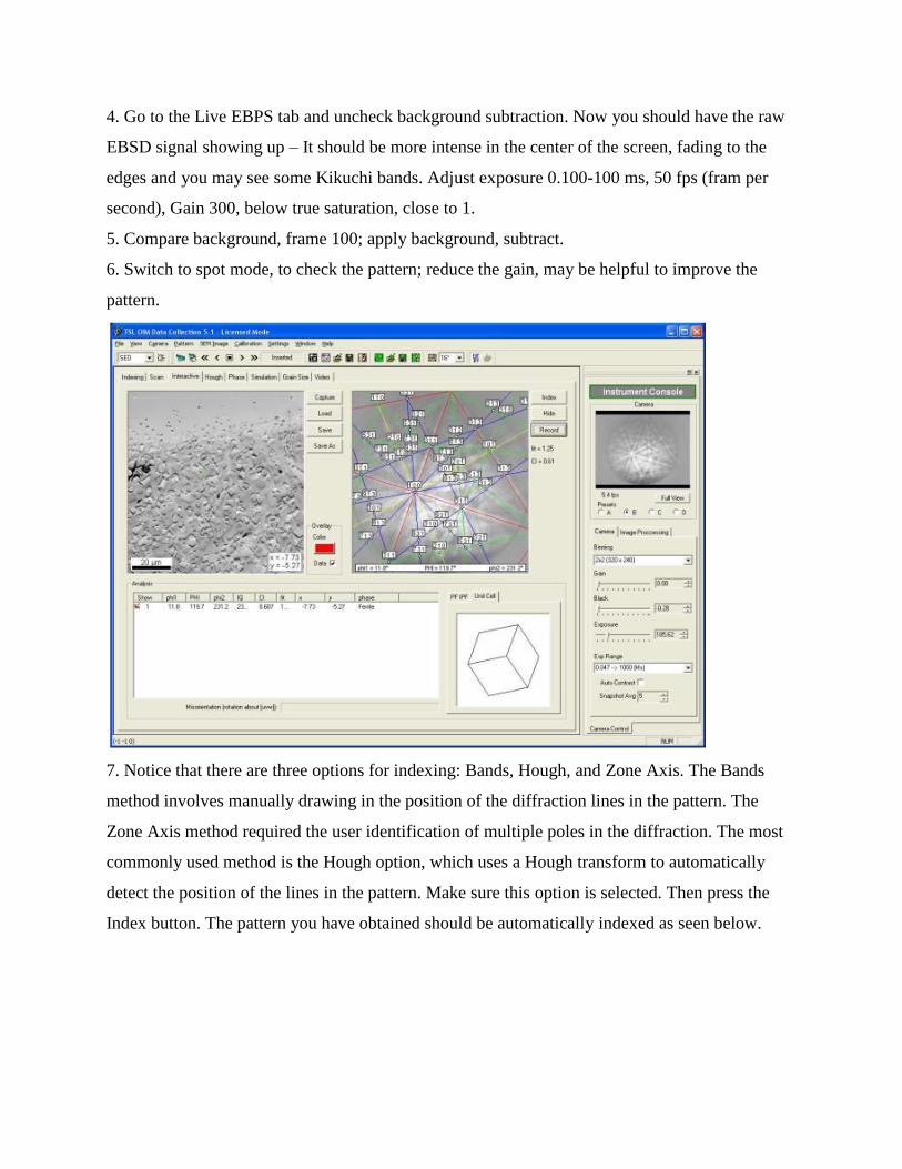
4. Go to the Live EBPS tab and uncheck background subtraction. Now you should have the raw
EBSD signal showing up – It should be more intense in the center of the screen, fading to the
edges and you may see some Kikuchi bands. Adjust exposure 0.100-100 ms, 50 fps (fram per
second), Gain 300, below true saturation, close to 1.
5. Compare background, frame 100; apply background, subtract.
6. Switch to spot mode, to check the pattern; reduce the gain, may be helpful to improve the
pattern.
7. Notice that there are three options for indexing: Bands, Hough, and Zone Axis. The Bands
method involves manually drawing in the position of the diffraction lines in the pattern. The
Zone Axis method required the user identification of multiple poles in the diffraction. The most
commonly used method is the Hough option, which uses a Hough transform to automatically
detect the position of the lines in the pattern. Make sure this option is selected. Then press the
Index button. The pattern you have obtained should be automatically indexed as seen below.
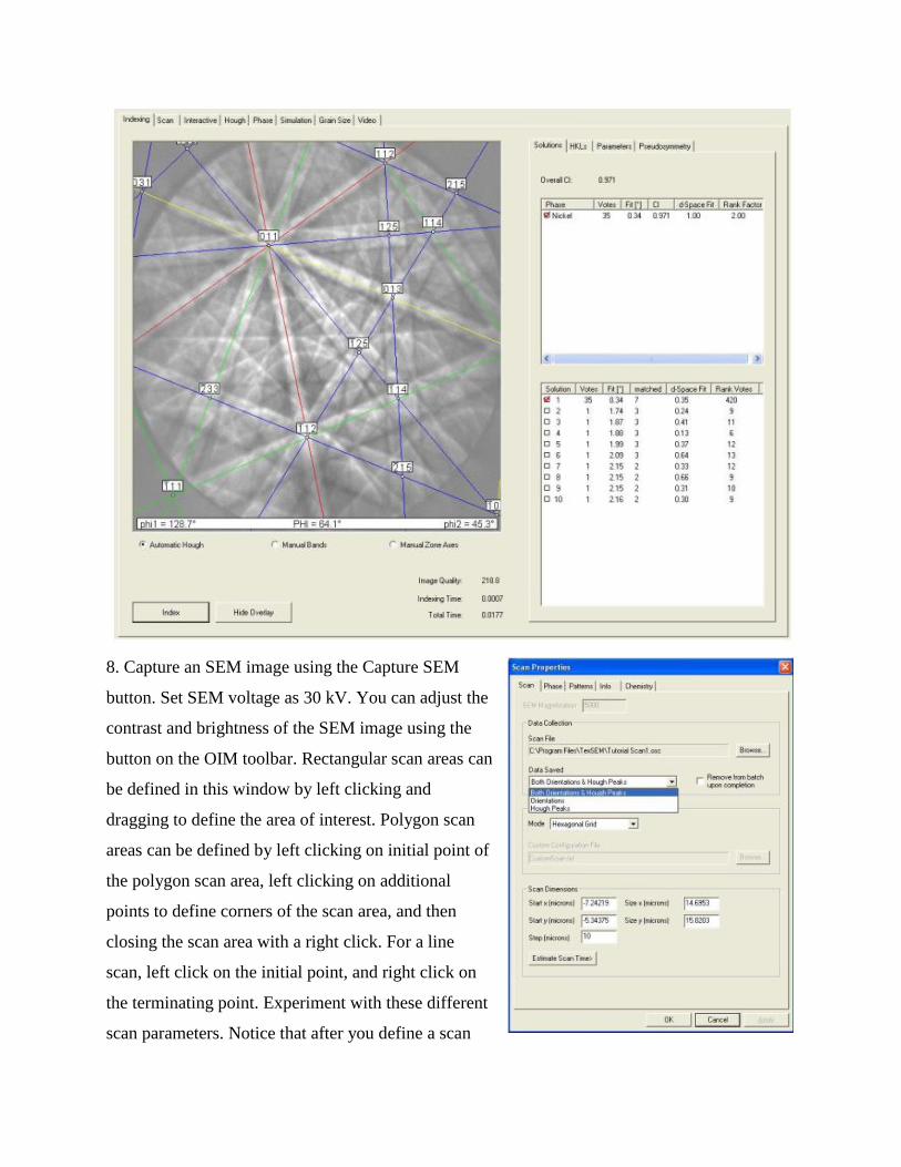
8. Capture an SEM image using the Capture SEM
button. Set SEM voltage as 30 kV. You can adjust the
contrast and brightness of the SEM image using the
button on the OIM toolbar. Rectangular scan areas can
be defined in this window by left clicking and
dragging to define the area of interest. Polygon scan
areas can be defined by left clicking on initial point of
the polygon scan area, left clicking on additional
points to define corners of the scan area, and then
closing the scan area with a right click. For a line
scan, left click on the initial point, and right click on
the terminating point. Experiment with these different
scan parameters. Notice that after you define a scan
area, the Scan Properties dialogue box appear. Save data both Orientations & Hough Peaks.
Orientation means that the Euler angles describing the orientation associated with each point in a
scan will be recorded. Hough Peaks means that the parameters associated with the peaks in
Hough Transform will be saved for each point in the scan. Scan type-hexagonal grid for Ni, scan
resolution-fine/medium.
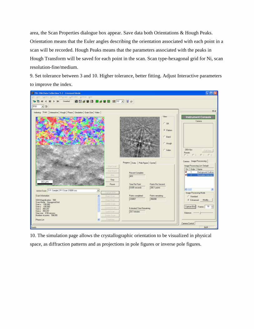
9. Set tolerance between 3 and 10. Higher tolerance, better fitting. Adjust Interactive parameters
to improve the index.
10. The simulation page allows the crystallographic orientation to be visualized in physical
space, as diffraction patterns and as projections in pole figures or inverse pole figures.
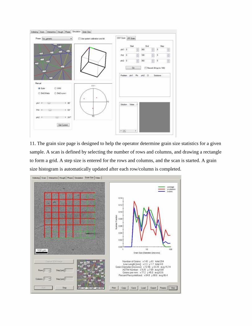
11. The grain size page is designed to help the operator determine grain size statistics for a given
sample. A scan is defined by selecting the number of rows and columns, and drawing a rectangle
to form a grid. A step size is entered for the rows and columns, and the scan is started. A grain
size histogram is automatically updated after each row/column is completed.
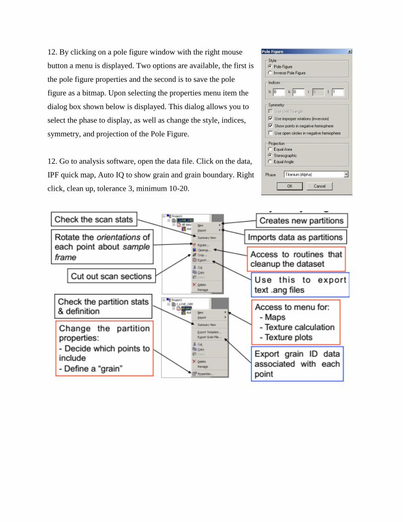
12. By clicking on a pole figure window with the right mouse
button a menu is displayed. Two options are available, the first is
the pole figure properties and the second is to save the pole
figure as a bitmap. Upon selecting the properties menu item the
dialog box shown below is displayed. This dialog allows you to
select the phase to display, as well as change the style, indices,
symmetry, and projection of the Pole Figure.
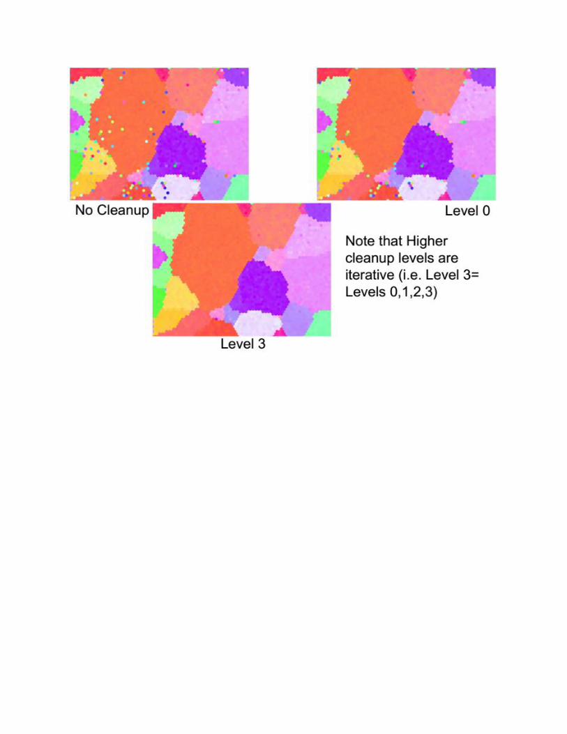
12. Go to analysis software, open the data file. Click on the data,
IPF quick map, Auto IQ to show grain and grain boundary. Right
click, clean up, tolerance 3, minimum 10-20.