Embed Size (px)
Citation preview
Standard based Instrumentation schemes for
3D SoC
Neal StollonChairman, Nexus 5001 Forum
www.nexus5001.org
Neal Stollon, Ph.D, P.E.
Chairman, Nexus 5001 Forum
Ph 972 458 9625
Neal Stollon is chairman of the 5001 Nexus Forum, which provides industry support for IEEE ISTO Nexus 5001 and related instrumentation standardization efforts. He has a Ph.D in EE from Southern Methodist University and is a licensed P.E., and has a decade of experience in debug architectures and instrumentation issues, on top of another decade or so of processor and SoC experience at TI, LSI Logic, MIPS, and elsewhere. Dr. Stollon is CTO at HDL Dynamics, providing systems analysis and consulting on embedded IP and instrumentation solutions for digital systems He is also the author of the book “On Chip Instrumentation: Design and Debug for Systems on Chip ”. He may be reached at [email protected]
Author Information
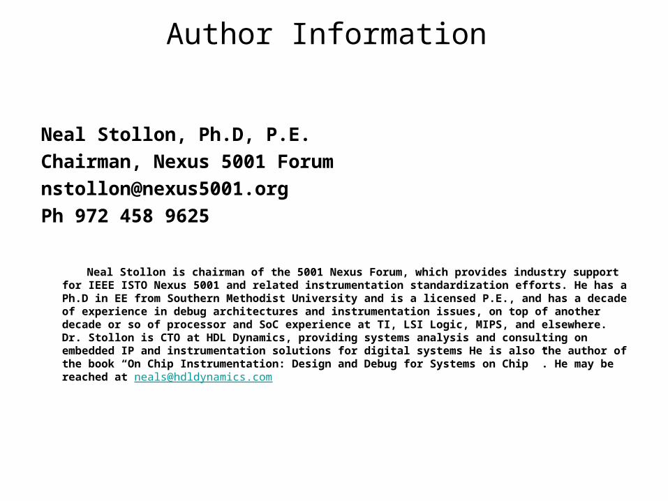
Standard based Instrumentation schemes for 3D SoC Abstract
Stacked multi-die and 3D SoC are being prototyped as a next generation for increasing silicon complexity. Complex designs increasingly require means for on-chip debug and interactive access and analysis instrumentation.
The complexities and interconnect limitations of 3D SoC make on-chip debug and instrumentation challenging, especially as they must be compatible with other standards being developed for heterogeneous 3D stacks. On-chip debug and instrumentation must interoperate with existing (i.e. JTAG) and proposed test strategies (i.e. PAR 1838) for 3D SoC.
Key requirements for a 3D SoC debug and instrumentation environment map against proposed solutions, One is based on the IEEE 5001 Nexus standard.
Nexus instrumentation features meet several of the key requirements for 3D SoC
including low pin and via options for high performance debug interfaces between die layers support for heterogeneous and multi-core systems
Interface standards should support both debug control and data trace in ways that are compatible with proposed 3D SoC test schemes.
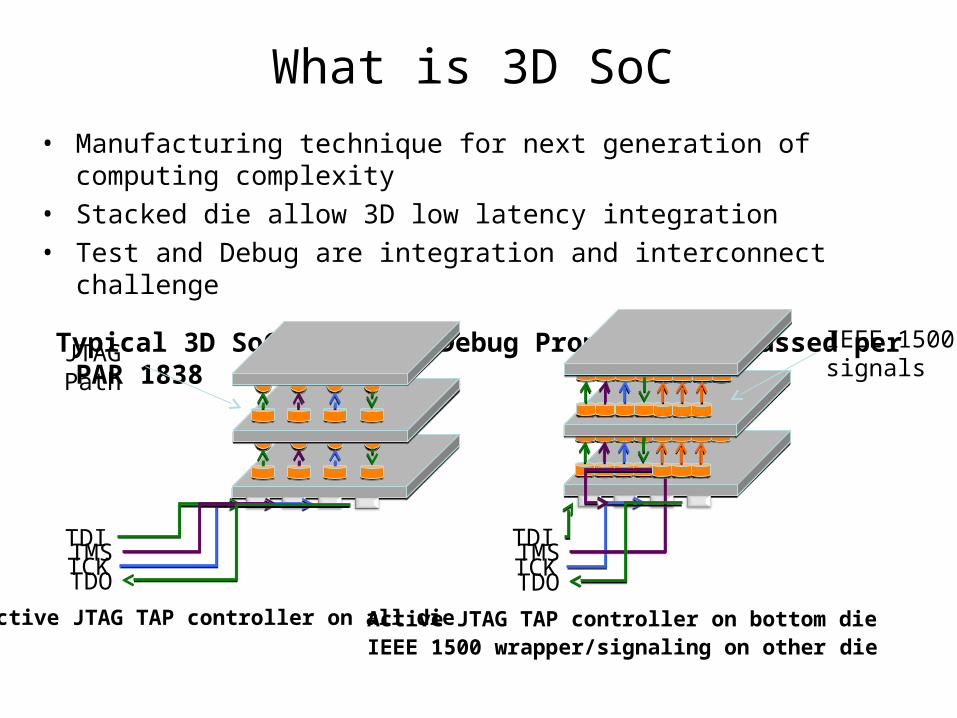
What is 3D SoC
• Manufacturing technique for next generation of computing complexity • Stacked die allow 3D low latency integration • Test and Debug are integration and interconnect challenge
Typical 3D SoC Test and Debug Proposals discussed per PAR 1838
Active JTAG TAP controller on all die Active JTAG TAP controller on bottom dieIEEE 1500 wrapper/signaling on other die
TCKTMSTDI
TDO TCKTMSTDI
TDO
JTAGPath
IEEE 1500signals
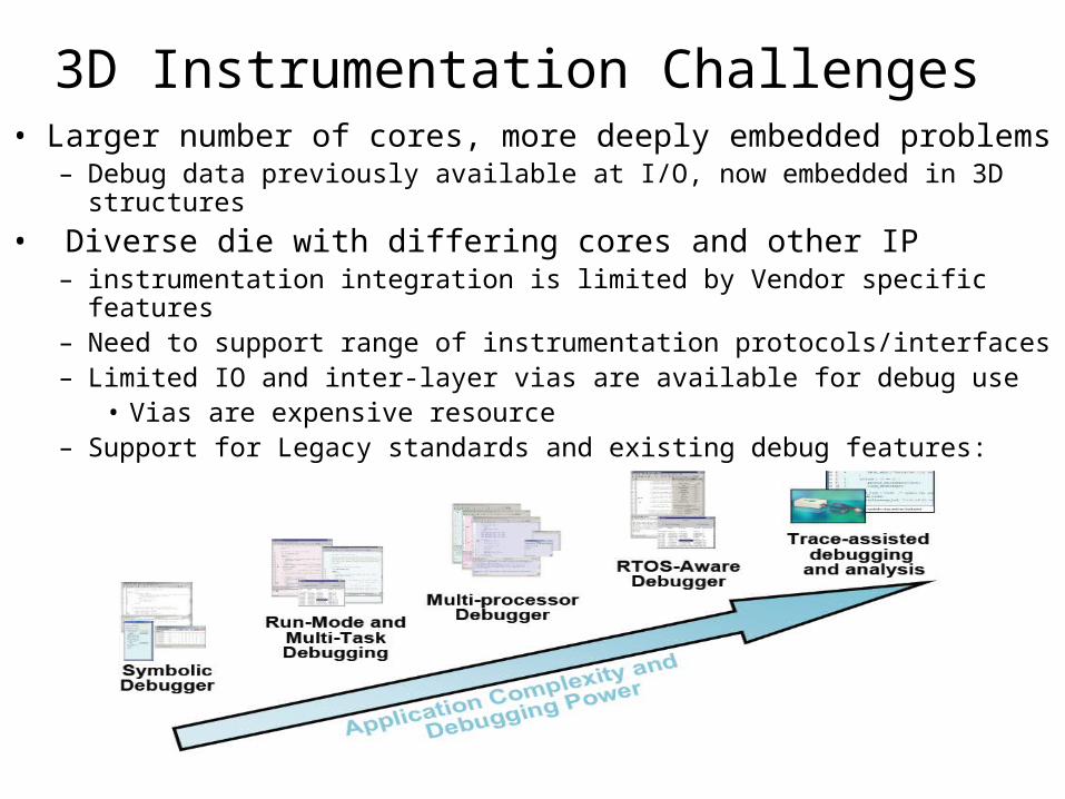
3D Instrumentation Challenges• Larger number of cores, more deeply embedded problems
– Debug data previously available at I/O, now embedded in 3D structures
• Diverse die with differing cores and other IP– instrumentation integration is limited by Vendor specific features– Need to support range of instrumentation protocols/interfaces– Limited IO and inter-layer vias are available for debug use
• Vias are expensive resource– Support for Legacy standards and existing debug features:
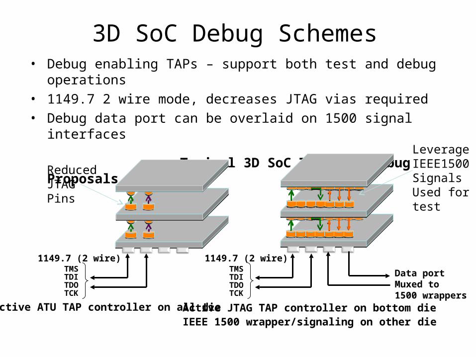
3D SoC Debug Schemes• Debug enabling TAPs – support both test and debug operations• 1149.7 2 wire mode, decreases JTAG vias required• Debug data port can be overlaid on 1500 signal interfaces
Typical 3D SoC Test and Debug Proposals
Active ATU TAP controller on all die Active JTAG TAP controller on bottom dieIEEE 1500 wrapper/signaling on other die
Data port Muxed to 1500 wrappers
1149.7 (2 wire)TMSTDITDOTCK
TMSTDITDOTCK
1149.7 (2 wire)
ReducedJTAGPins
LeverageIEEE1500SignalsUsed for test
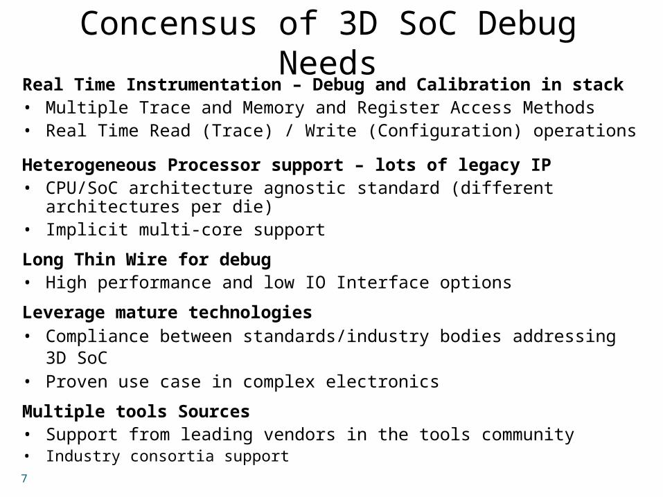
Concensus of 3D SoC Debug NeedsReal Time Instrumentation – Debug and Calibration in stack • Multiple Trace and Memory and Register Access Methods• Real Time Read (Trace) / Write (Configuration) operations
Heterogeneous Processor support – lots of legacy IP• CPU/SoC architecture agnostic standard (different architectures per die)• Implicit multi-core support
Long Thin Wire for debug • High performance and low IO Interface options
Leverage mature technologies
• Compliance between standards/industry bodies addressing 3D SoC • Proven use case in complex electronics
Multiple tools Sources• Support from leading vendors in the tools community• Industry consortia support
7
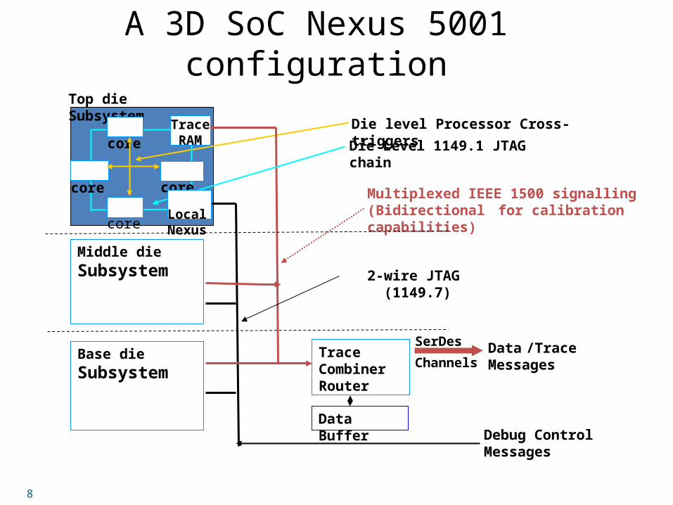
A 3D SoC Nexus 5001 configuration
Debug ControlMessages
Base die
Subsystem
Middle die
Subsystem
Top die Subsystem
Trace CombinerRouter
Data /Trace Messages
SerDes
Channels
2-wire JTAG (1149.7)
core
core core
core
Trace RAM
Data Buffer
Die Level 1149.1 JTAG chain
Die level Processor Cross-triggers
Multiplexed IEEE 1500 signalling(Bidirectional for calibration capabilities)
LocalNexus
8
9
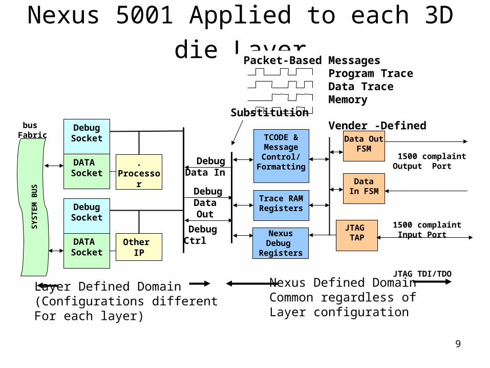
Nexus 5001 Applied to each 3D die Layer
1500 complaint Output Port
1500 complaint Input Port
JTAG TDI/TDO
DebugSocket
Data In FSM
Data Out FSM
JTAG TAP
TCODE & Message Control/
Formatting
Trace RAM Registers
NexusDebug
Registers
Debug Ctrl
Debug Data Out
DebugData In
.Processor
DATA Socket
DebugSocket
Other IP
DATA Socket
Nexus Defined DomainCommon regardless of Layer configuration
Layer Defined Domain(Configurations different For each layer)
bus Fabric
SY
ST
EM
BU
S
Packet-Based MessagesProgram TraceData TraceMemory SubstitutionVender -Defined
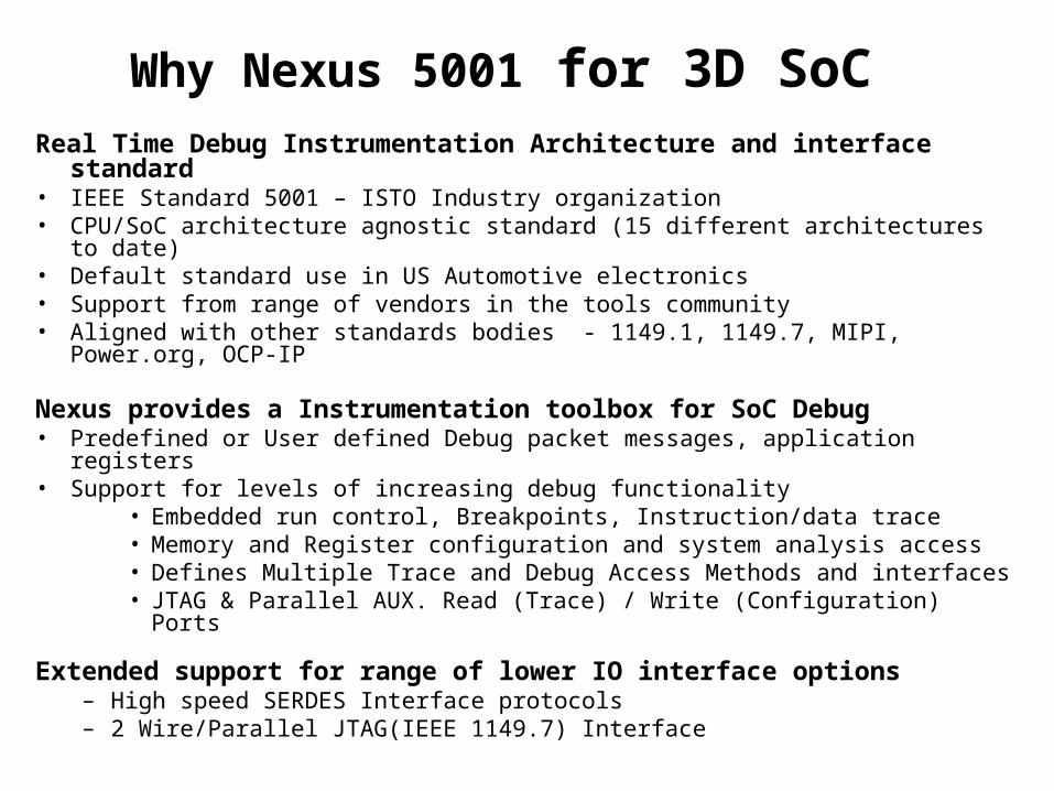
Why Nexus 5001 for 3D SoCReal Time Debug Instrumentation Architecture and interface standard • IEEE Standard 5001 – ISTO Industry organization • CPU/SoC architecture agnostic standard (15 different architectures to date)• Default standard use in US Automotive electronics• Support from range of vendors in the tools community• Aligned with other standards bodies - 1149.1, 1149.7, MIPI, Power.org, OCP-IP
Nexus provides a Instrumentation toolbox for SoC Debug• Predefined or User defined Debug packet messages, application registers • Support for levels of increasing debug functionality
• Embedded run control, Breakpoints, Instruction/data trace • Memory and Register configuration and system analysis access• Defines Multiple Trace and Debug Access Methods and interfaces• JTAG & Parallel AUX. Read (Trace) / Write (Configuration) Ports
Extended support for range of lower IO interface options– High speed SERDES Interface protocols– 2 Wire/Parallel JTAG(IEEE 1149.7) Interface
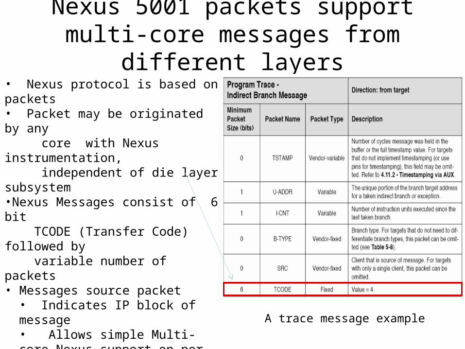
Nexus 5001 packets support multi-core messages from different layers
• Nexus protocol is based on packets• Packet may be originated by any core with Nexus instrumentation, independent of die layer subsystem•Nexus Messages consist of 6 bit TCODE (Transfer Code) followed by variable number of packets• Messages source packet
• Indicates IP block of message • Allows simple Multi-core Nexus support on per message basis
• Each message contains optional timestamp for data synchronization• Vendor packets are allow user specific commands and operations
A trace message example
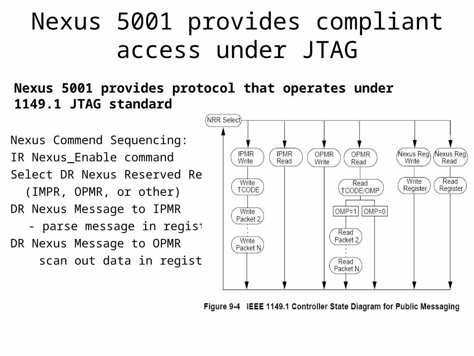
Nexus 5001 provides compliant access under JTAG
Nexus Commend Sequencing:
IR Nexus_Enable command
Select DR Nexus Reserved Register
(IMPR, OPMR, or other)
DR Nexus Message to IPMR
- parse message in register
DR Nexus Message to OPMR
scan out data in register
Nexus 5001 provides protocol that operates under 1149.1 JTAG standard
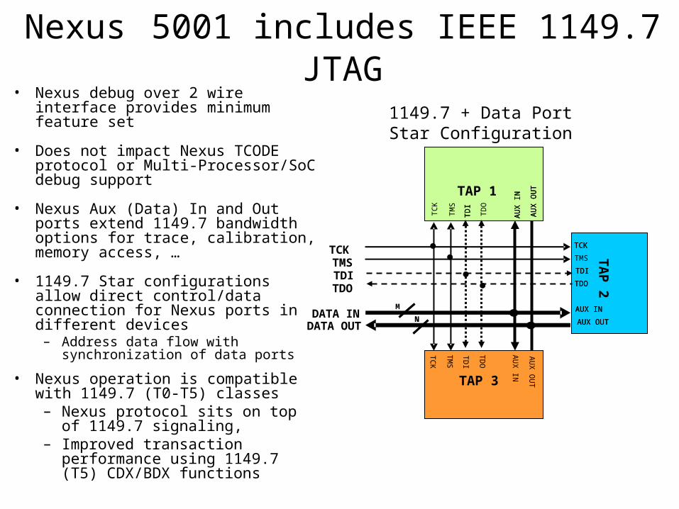
Nexus 5001 includes IEEE 1149.7 JTAG• Nexus debug over 2 wire interface
provides minimum feature set
• Does not impact Nexus TCODE protocol or Multi-Processor/SoC debug support
• Nexus Aux (Data) In and Out ports extend 1149.7 bandwidth options for trace, calibration, memory access, …
• 1149.7 Star configurations allow direct control/data connection for Nexus ports in different devices
– Address data flow with synchronization of data ports
• Nexus operation is compatible with 1149.7 (T0-T5) classes – Nexus protocol sits on top of
1149.7 signaling, – Improved transaction
performance using 1149.7 (T5) CDX/BDX functions
1149.7 + Data PortStar Configuration
DATA OUTDATA IN
N
TCK TMS TDITDO
M
N
TA
P 2
TCK
TMS
TDI
TDO
AUX IN
AUX OUT
TCK
TDI
TDO
AUX IN
AUX OUT
TC
K
TM
S
TD
I
AU
X I
N
AU
X O
UT
TD
I
TD
O
AU
X I
N
AU
X O
UT
TC
K
TM
S
TD
I
TD
O
AU
X IN
AU
X O
UT
TAP 1
TAP 3
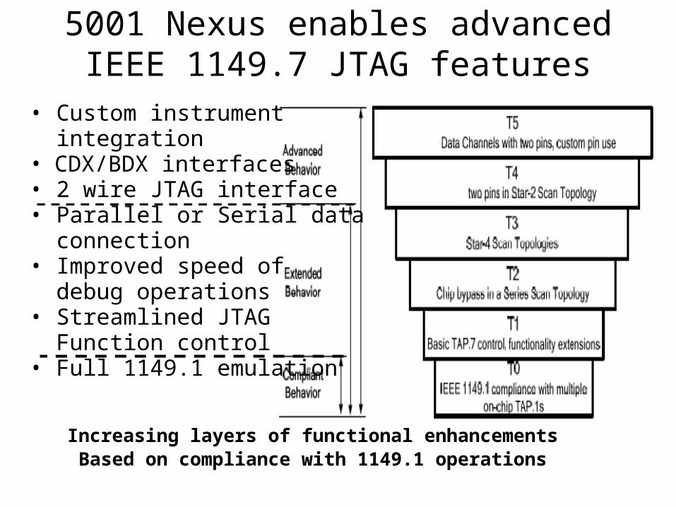
5001 Nexus enables advanced IEEE 1149.7 JTAG features
• Custom instrument integration • CDX/BDX interfaces• 2 wire JTAG interface• Parallel or Serial data connection• Improved speed of debug operations• Streamlined JTAG Function control• Full 1149.1 emulation
Increasing layers of functional enhancementsBased on compliance with 1149.1 operations
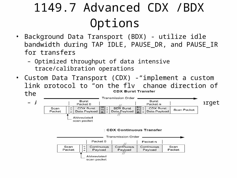
1149.7 Advanced CDX /BDX Options • Background Data Transport (BDX) - utilize idle bandwidth during
TAP IDLE, PAUSE_DR, and PAUSE_IR for transfers– Optimized throughput of data intensive trace/calibration operations
• Custom Data Transport (CDX) - implement a custom link protocol to “on the fly” change direction of the data transfers.– Allows Nexus data transfers to be driven from target
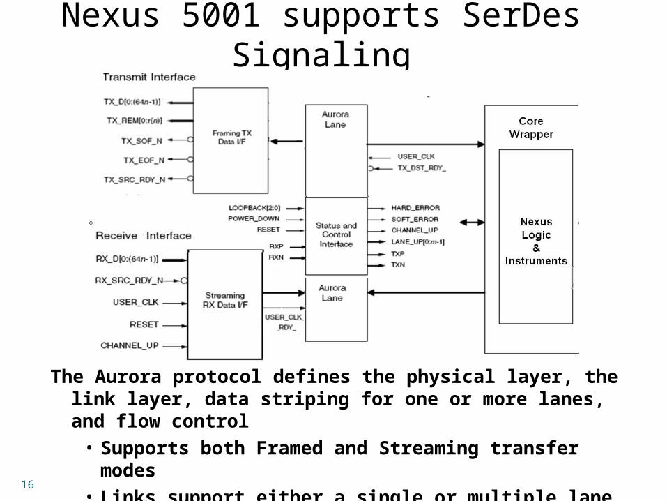
Nexus 5001 supports SerDes Signaling
The Aurora protocol defines the physical layer, the link layer, data striping for one or more lanes, and flow control
• Supports both Framed and Streaming transfer modes• Links support either a single or multiple lane channels
16
Key points• We propose a Test compatible Debug Port implementation
– 1500 and Parallel data ports operate under a common framework • Nexus provides infrastructure for needed 3D SoC – Packet based commands simplify 3D internal connections • Nexus-2012 standard adds access port options compatible with 3D SoC
– SERDES protocol at base layer• Debug data can be transferred as very fast add/drop port • Leverages the very low latencies between 3D die layers
– 1149.7 • 2 wire option reduces number of through vias required• Nexus Message can be treated as JTAG Rd/Wr register • 1149.7 FSM are local to the per layer Port implementation• Differing layers may have different instrumentation
• This discusses work in progress• This presentation leverages concepts and work from IEEE PAR 1838
(3D Test Access Group) and IEEE 1500 (Embedded Core Test Group) – it has not been approved by either group.