Embed Size (px)
Citation preview
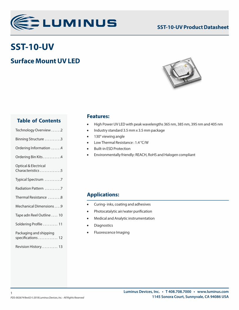
Table of Contents
Technology Overview . . . . . .2
Binning Structure . . . . . . . . . .3
Ordering Information . . . . . .4
Ordering Bin Kits . . . . . . . . . . .4
Optical & Electrical Characteristics . . . . . . . . . . . . .5
Typical Spectrum . . . . . . . . . .7
Radiation Pattern . . . . . . . . . .7
Thermal Resistance . . . . . . . .8
Mechanical Dimensions . . . .9
Tape adn Reel Outline . . . . 10
Soldering Profile . . . . . . . . . 11
Packaging and shipping specifications . . . . . . . . . . . . 12
Revision History . . . . . . . . . . 13
SST-10-UVSurface Mount UV LED
1PDS-002674 Rev02 © 2018 Luminus Devices, Inc. - All Rights Reserved
Luminus Devices, Inc. • T 408.708.7000 • www.luminus.com1145 Sonora Court, Sunnyvale, CA 94086 USA
• Curing- inks, coating and adhesives
• Photocatalytic air/water purification
• Medical and Analytic instrumentation
• Diagnostics
• Fluorescence Imaging
Features: • High Power UV LED with peak wavelengths 365 nm, 385 nm, 395 nm and 405 nm
• Industry standard 3 .5 mm x 3 .5 mm package
• 130° viewing angle
• Low Thermal Resistance : 1 .4 °C/W
• Built-in ESD Protection
• Environmentally friendly: REACH, RoHS and Halogen compliant
SST-10-UV Product Datasheet
Applications:

2PDS-002674 Rev02 © 2018 Luminus Devices, Inc. - All Rights Reserved
Luminus Devices, Inc. • T 408.708.7000 • www.luminus.com1145 Sonora Court, Sunnyvale, CA 94086 USA
CBM-40-UVX Product Datasheet
Technology Overview
Luminus LEDs benefit from innovations in device technology, chip packaging and thermal management . This suite of technologies give engineers and system designers the freedom to develop solutions high both in power and in efficiency .
Luminus Surface Mount LED Technology
Luminus’ vertical chip technology enables uniform and high brightness over the entire chip surface .
Thermal management is critical in high power LED applications . With a thermal resistance (Rth) from junction to board of 1 .4 ºC/W, the SST-10 has one of the lowest thermal resistances of UV LEDs in the market . The low Rth, along with Luminus vertical chip techology allows users to drive the LEDs at high current densities while maintaining a low junction temperature, thereby resulting in brighter solutions and longer lifetimes . Reliability
Luminus LEDs are one of the most reliable light sources in the world . They pass a rigorous suite of environmental and mechanical stress tests, including mechanical shock, vibration, temperature cycling and humidity, and have been qualified for use in high power and high current applications . Luminus UV LEDs are designed for the most demanding applications with median lifetimes exceeding 30,000 hours .
Environmental Benefits
Luminus LEDs help reduce power consumption and the amount of hazardous waste entering the environment . All Luminus LEDs are RoHS and Halogen compliant and free of hazardous materials, including lead and mercury .
SST-10-UV Product Datasheet
Luminus Devices, Inc. • T 408.708.7000 • www.luminus.com1145 Sonora Court, Sunnyvale, CA 94086 USA
SST-10-UV Product Datasheet
3PDS-002674 Rev02 © 2018 Luminus Devices, Inc. - All Rights Reserved
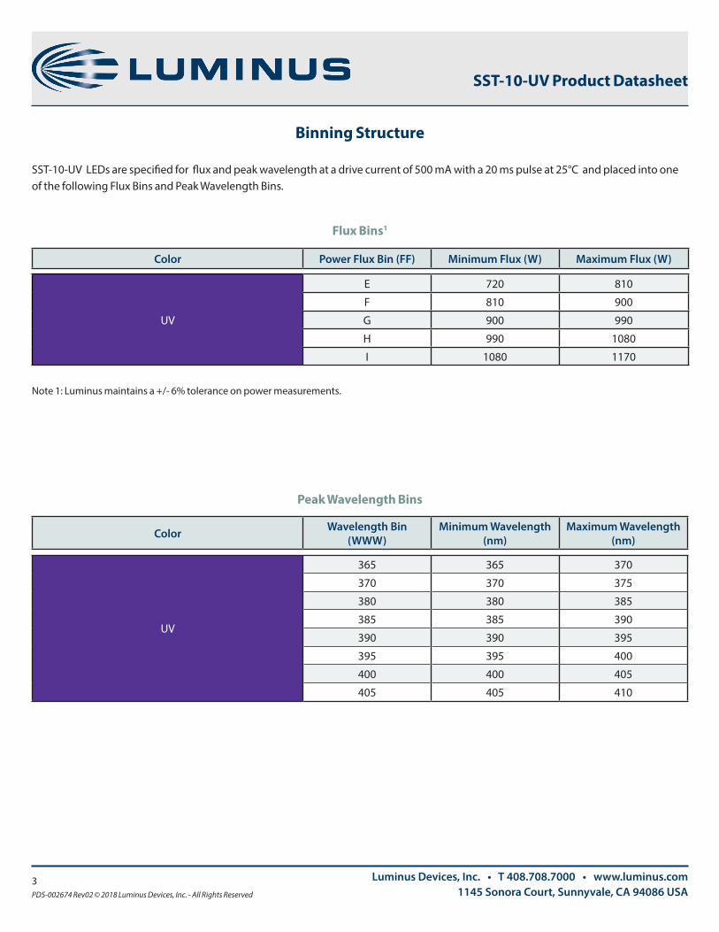
Binning Structure
SST-10-UV LEDs are specified for flux and peak wavelength at a drive current of 500 mA with a 20 ms pulse at 25°C and placed into one of the following Flux Bins and Peak Wavelength Bins .
Color Power Flux Bin (FF) Minimum Flux (W) Maximum Flux (W)
UV
E 720 810
F 810 900
G 900 990
H 990 1080
I 1080 1170
Note 1: Luminus maintains a +/- 6% tolerance on power measurements .
Color Wavelength Bin (WWW)
Minimum Wavelength (nm)
Maximum Wavelength (nm)
UV
365 365 370
370 370 375
380 380 385
385 385 390
390 390 395
395 395 400
400 400 405
405 405 410
Flux Bins1
Peak Wavelength Bins

Ordering Information
Products Ordering Part Number Description
SST-10-UVSST-10-UV-A130-FFWWW-00SST-10-UV-B130-FFWWW-00
UV LED in a 3535 surface mount package with a 130 degree molded lens
Luminus Devices, Inc. • T 408.708.7000 • www.luminus.com1145 Sonora Court, Sunnyvale, CA 94086 USA
Note 1: Refer to drawings on page 9 for details on "A" and "B" solder pad layoutsNote 2: A Bin Kit represents a group of flux and wavelength bins that are shippable for a given ordering part number . Individual bins are not orderable . . Note 3: Flux Bin listed is minimum bin shipped - higher bins may be included at Luminus’ discretion
Part Number Nomenclature
Product Family Chip Area Color Package Configuration 1 Bin Kit 2,3
SST: Surface Mount package 10: 1 mm2 UV = Ultraviolet
A130 : "A" solder pad layout and 130 ° lens B130 : "B" solder pad layout and 130 ° lens
See ordering bin kits table below for
complete bindefinition
SST 10 UV X130 FFWWW-00
SST-10-UV Product Datasheet
4PDS-002674 Rev02 © 2018 Luminus Devices, Inc. - All Rights Reserved
Ordering Bin Kits
Wavelength Range (nm)Luminous Flux
Wavelength BinsOrdering
Bin Kit NumberBin Kit Flux Code
Min . Flux (mW)
365-375E 720 365, 370 E365-00
F 810 365, 375 F365-00
380-390 G 900 380, 385 G385-00
390-400 G 900 390, 395 G395-00
400-410 F 810 400,405 F405-00

Optical & Electrical Characteristics (Ths = 25°C)
UV
Parameter Symbol Values 4 Unit
Peak Wavelength Range λ 365-375 380-390 390-400 400-410 nm
Test Current for binning 5 I 500 500 500 500 mA
Peak Wavelength Typ . λp 370 385 395 405 nm
Forward Voltage
VF min 3 .0 3 .0 3 .0 3 .0 V
VF 3 .7 3 .4 3 .3 3 .3 V
VF max 4 .0 4 .0 4 .0 4 .0 V
Radiometric Flux 6 Φtyp 875 1015 1015 930 mW
FWHM at 50% of Φ Δλ1/2 10 10 10 10 nm
Viewing Angle 2Φ1/2 130 130 130 130 degrees
Parameter Symbol Values
Absolute Maximum Current (CW) 7 Imax365 nm- 1A
385-405 nm- 1 .5 A
Maximum Junction Temperature 7 Tjmax 100 °C
Storage Temperature Range Ts
-40 to +100 °C
Soldering Temperature Tsld JEDEC J-STD-020C, 260 °C
ESD Sensitivity (HBM) Vb 6000 V
Note 4: Unless otherwise noted, values listed are typical. Devices are production tested and specified at 500 mA with a 20 ms pulse at 25°C .
Note 5: While SST-10-UV devices are tested at 500 mA, they can be driven at CW currents ranging from 200 mA to 1.5 A and at duty cycles ranging from 1% to 100%. Drive current and duty cycle should be adjusted as necessary to maintain the junction temperature desired to meet application lifetime requirements.
Note 6: Typical radiometric flux is for reference only. Minimum flux values are guaranteed based on the bin kit ordered. For product roadmap and future performance of devices, contact Luminus.
Note 7: SST-10-UV LEDs are designed for operation to an absolute maximum current as specified above. Product lifetime data is specified at or below maximum drive current. Sustained operation beyond absolute maximum currents will result in a reduction of device life time . Actual device lifetimes will also depend on junction temperature and operation beyond maximum junction temperature is not recommended. Contact Luminus for lifetime derating curves and for further information. In pulsed operation, rise time from 10-90% of forward current should be longer than 0.5 μseconds.
Luminus Devices, Inc. • T 408.708.7000 • www.luminus.com1145 Sonora Court, Sunnyvale, CA 94086 USA
SST-10-UV Product Datasheet
5PDS-002674 Rev02 © 2018 Luminus Devices, Inc. - All Rights Reserved
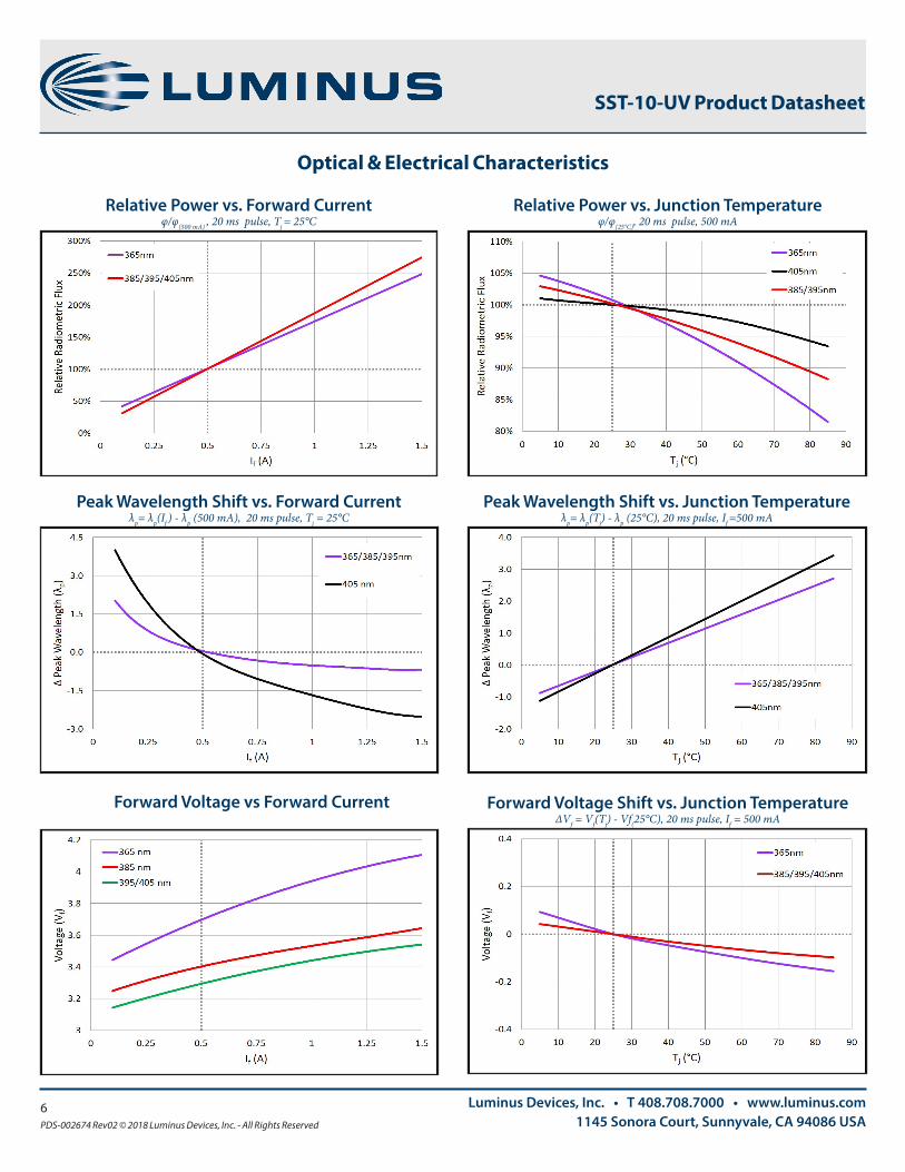
Optical & Electrical Characteristics
Luminus Devices, Inc. • T 408.708.7000 • www.luminus.com1145 Sonora Court, Sunnyvale, CA 94086 USA
Relative Power vs. Forward Currentφ/φ(500 mA) , 20 ms pulse, Tj = 25°C
Forward Voltage vs Forward Current
SST-10-UV Product Datasheet
6PDS-002674 Rev02 © 2018 Luminus Devices, Inc. - All Rights Reserved
Peak Wavelength Shift vs. Forward Currentλp= λp(If ) - λp (500 mA), 20 ms pulse, Tj = 25°C
Peak Wavelength Shift vs. Junction Temperatureλp= λp(Tj) - λp (25°C), 20 ms pulse, If =500 mA
Forward Voltage Shift vs. Junction TemperatureΔVf = Vf(Tj) - Vf(25°C), 20 ms pulse, If = 500 mA
Relative Power vs. Junction Temperatureφ/φ(25°C), 20 ms pulse, 500 mA
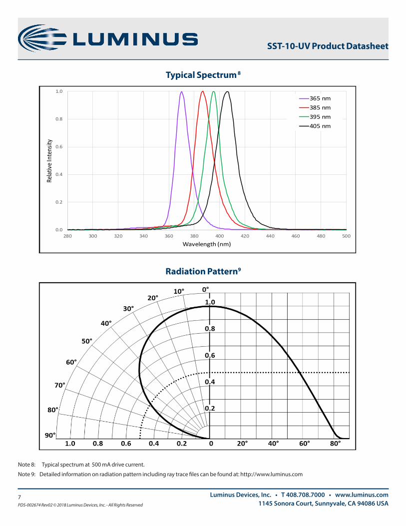
Note 8: Typical spectrum at 500 mA drive current .
Note 9: Detailed information on radiation pattern including ray trace files can be found at: http://www .luminus .com
Typical Spectrum 8
Luminus Devices, Inc. • T 408.708.7000 • www.luminus.com1145 Sonora Court, Sunnyvale, CA 94086 USA
0.0
0.2
0.4
0.6
0.8
1.0
280 300 320 340 360 380 400 420 440 460 480 500
Relat
ive In
tens
ity
Wavelength (nm)
365 nm385 nm395 nm405 nm
Radiation Pattern9
SST-10-UV Product Datasheet
7PDS-002674 Rev02 © 2018 Luminus Devices, Inc. - All Rights Reserved

Luminus Devices, Inc. • T 408.708.7000 • www.luminus.com1145 Sonora Court, Sunnyvale, CA 94086 USA
Thermal Resistance
Note 10: Electrical thermal resistance based on input electrical power at 500 mA and measured per JESD51-14
Ths de�nition = 3 mm from core-board
Tj
Tc
Ths
Die Junction
Window Frame
Ceramic Substrate
Aluminum Core Board
Heat Sink
Tb
Dome
Rθj-b10 1.4 °C/W
SST-10-UV Product Datasheet
8PDS-002674 Rev02 © 2018 Luminus Devices, Inc. - All Rights Reserved

Mechanical Dimensions - A130 package
Luminus Devices, Inc. • T 408.708.7000 • www.luminus.com1145 Sonora Court, Sunnyvale, CA 94086 USA
SST-10-UV Product Datasheet
9PDS-002674 Rev02 © 2018 Luminus Devices, Inc. - All Rights Reserved
Mechanical Dimensions - B130 package
DWG-002848
DWG-003005

Luminus Devices, Inc. • T 408.708.7000 • www.luminus.com1145 Sonora Court, Sunnyvale, CA 94086 USA
Tape and Reel Outline
SST-10-UV Product Datasheet
10PDS-002674 Rev02 © 2018 Luminus Devices, Inc. - All Rights Reserved
Luminus Devices, Inc. • T 408.708.7000 • www.luminus.com1145 Sonora Court, Sunnyvale, CA 94086 USA
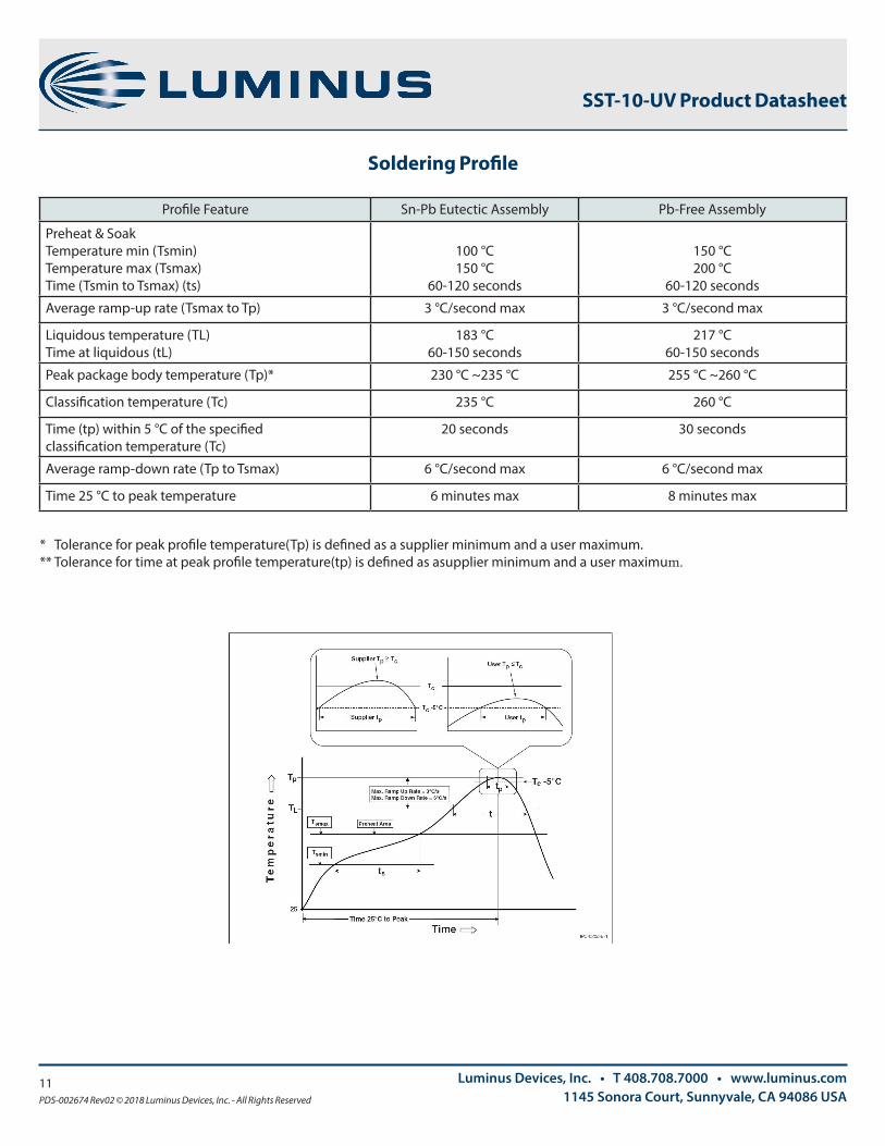
Soldering Profile
SST-10-UV Product Datasheet
11PDS-002674 Rev02 © 2018 Luminus Devices, Inc. - All Rights Reserved
Profile Feature Sn-Pb Eutectic Assembly Pb-Free Assembly
Preheat & SoakTemperature min (Tsmin)Temperature max (Tsmax)Time (Tsmin to Tsmax) (ts)
100 °C150 °C
60-120 seconds
150 °C200 °C
60-120 seconds
Average ramp-up rate (Tsmax to Tp) 3 °C/second max 3 °C/second max
Liquidous temperature (TL)Time at liquidous (tL)
183 °C60-150 seconds
217 °C60-150 seconds
Peak package body temperature (Tp)* 230 °C ~235 °C 255 °C ~260 °C
Classification temperature (Tc) 235 °C 260 °C
Time (tp) within 5 °C of the specifiedclassification temperature (Tc)
20 seconds 30 seconds
Average ramp-down rate (Tp to Tsmax) 6 °C/second max 6 °C/second max
Time 25 °C to peak temperature 6 minutes max 8 minutes max
* Tolerance for peak profile temperature(Tp) is defined as a supplier minimum and a user maximum .** Tolerance for time at peak profile temperature(tp) is defined as asupplier minimum and a user maximum.

Luminus Devices, Inc. • T 408.708.7000 • www.luminus.com1145 Sonora Court, Sunnyvale, CA 94086 USA
Packing and Shipping Specifications
SST-10-UV Product Datasheet
12PDS-002674 Rev02 © 2018 Luminus Devices, Inc. - All Rights Reserved
Product Label Specification
Sample label –for illustration only
Shipping Box

Luminus Devices, Inc. • T 408.708.7000 • www.luminus.com1145 Sonora Court, Sunnyvale, CA 94086 USA
Revision History
SST-10-UV Product Datasheet
13PDS-002674 Rev02 © 2018 Luminus Devices, Inc. - All Rights Reserved
Rev Date Description of Change
01 06/01/2018 Initial Release
02 8/31/12018 Added "B130" version: updated ordering part numbers, characterization graphs and mechanical drawings
The products, their specifications and other information appearing in this document are subject to change by Luminus Devices without notice . Luminus Devices assumes no liability for errors that may appear in this document, and no liability otherwise arising from the application or use of the product or information contained herein . None of the information provided herein should be considered to be a representation of the fitness or suitability of the product for any particular application or as any other form of warranty . Luminus Devices’ product warranties are limited to only such warranties as accompany a purchase contract or purchase order for such products . Nothing herein is to be construed as constituting an additional warranty . No information contained in this publication may be considered as a waiver by Luminus Devices of any intellectual property rights that Luminus Devices may have in such information .
This product is protected by U .S . Patents 6,831,302; 7,074,631; 7,083,993; 7,084,434; 7,098,589; 7,105,861; 7,138,666; 7,166,870; 7,166,871; 7,170,100; 7,196,354; 7,211,831; 7,262,550; 7,274,043; 7,301,271; 7,341,880; 7,344,903; 7,345,416; 7,348,603; 7,388,233; 7,391,059 Patents Pending in the U .S . and other countries .
![A Dimensions: [mm] B Recommended land pattern: [mm] D ... · 1.1 1.0 REV 2014-12-16 2014-08-06 DATE SSt SSt BY BMoe BMoe CHECKED Würth Elektronik eiSos GmbH & Co. KG EMC & Inductive](https://img.pdfslide.us/doc/110x75/6037c9dbd60e5e1c6b763ad1/a-dimensions-mm-b-recommended-land-pattern-mm-d-11-10-rev-2014-12-16.jpg)
![A Dimensions: [mm] B Recommended land pattern: [mm] D ...2012-12-06 2012-10-24 2012-08-08 2012-06-28 2012-03-12 DATE SSt SSt SSt SSt SSt SSt BY SSt SSt BD BD SSt DDe CHECKED Würth](https://img.pdfslide.us/doc/110x75/60f984e176666848374d15c0/a-dimensions-mm-b-recommended-land-pattern-mm-d-2012-12-06-2012-10-24.jpg)


![A Dimensions: [mm] B Recommended land pattern: [mm] D ... · 2013-03-12 2013-01-13 2012-12-10 2012-10-29 2012-08-27 2006-05-05 DATE SSt SSt SSt SSt SSt SSt SSt BY SSt COt COt SSt](https://img.pdfslide.us/doc/110x75/604b228bc93c005c75431c51/a-dimensions-mm-b-recommended-land-pattern-mm-d-2013-03-12-2013-01-13.jpg)