Embed Size (px)
Citation preview
1. General description
The SSL3252 is a photo flash LED driver designed for battery operated mobile devices such as mobile phones and PDAs. The boost converter delivers high performance and drives a single or dual high brightness LED at up to 500 mA with over 85 % efficiency. The driver can be programmed to operate in Flash mode, Torch mode, Assist light mode, or Indicator mode.
The small silicon size and the high internal switching frequency of 2 MHz minimize the size of the application and make the SSL3252 very suitable for mobile phones where space is limited, and only requiring three external components. System protection has been a very important part of the SSL3252 design, so a time-out function can be programmed to prevent overstressing the LED, and the driver itself is protected from overheating.
2. Features and benefits
High power single or dual LED output driving up to 500 mA flash current
Separate indicator LED output of 2.5 mA to 10 mA
High side current source for main and indicator LEDs
Output voltage of up to 8.85 V
Wide input voltage ranging from 2.5 V to 5.5 V
High efficiency of over 85 % at optimum output current
Switching frequency of 2 MHz
Flash mode, Assist light mode, Torch mode and Indicator mode are supported
Internally timed flash operation up to 850 ms
I2C-bus, programmable up to 400 kHz
Strobe signal to avoid I2C latency for the flash
Direct enable signals for stand-alone operation
Forward voltage sensing to allow single/dual LED detection
Soft start/soft stop
Integrated protection circuits for enhanced system reliability:
Internal time-out
OverTemperature Protection (OTP)
UnderVoltage LockOut (UVLO)
OverVoltage Protection (OVP)
Short-circuit protection
Inductor peak current limit and broken coil detection
Low device shut-down current of less than 1 A
Small WLCSP12 package with 500 m bump pitch
SSL3252Photo flash LED driverRev. 1 — 7 July 2011 Product data sheet
NXP Semiconductors SSL3252Photo flash LED driver
3. Applications
Photo flash LED driver for mobile phones and digital cameras
White LED driver for battery powered portable devices
4. Ordering information
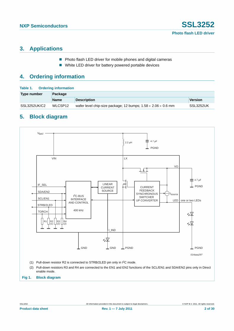
5. Block diagram
Table 1. Ordering information
Type number Package
Name Description Version
SSL3252UK/C2 WLCSP12 wafer level chip-size package; 12 bumps; 1.58 2.06 0.6 mm SSL3252UK
(1) Pull-down resistor R2 is connected to STRB/2LED pin only in I2C mode.
(2) Pull-down resistors R3 and R4 are connected to the EN1 and EN2 functions of the SCL/EN1 and SDA/EN2 pins only in Direct enable mode.
Fig 1. Block diagram
VBAT
IF_SEL
SDA/EN2
SCL/EN1
STRB/2LED
TORCH
I2C-BUSINTERFACE
AND CONTROL
LINEARCURRENTSOURCE
CURRENTFEEDBACK
SYNCHRONOUSSWITCHER
UP CONVERTER
014aaa297
4.7 µF
4.7 µF2.2 µH
one or two LEDs
GND GND PGND PGND
PGND
I_IND
LED
VIN
VO
LX
Isource
PGND
400 kHz
R1 R2 R3 R4(2)(2)(1)
SSL3252 All information provided in this document is subject to legal disclaimers. © NXP B.V. 2011. All rights reserved.
Product data sheet Rev. 1 — 7 July 2011 2 of 30
NXP Semiconductors SSL3252Photo flash LED driver
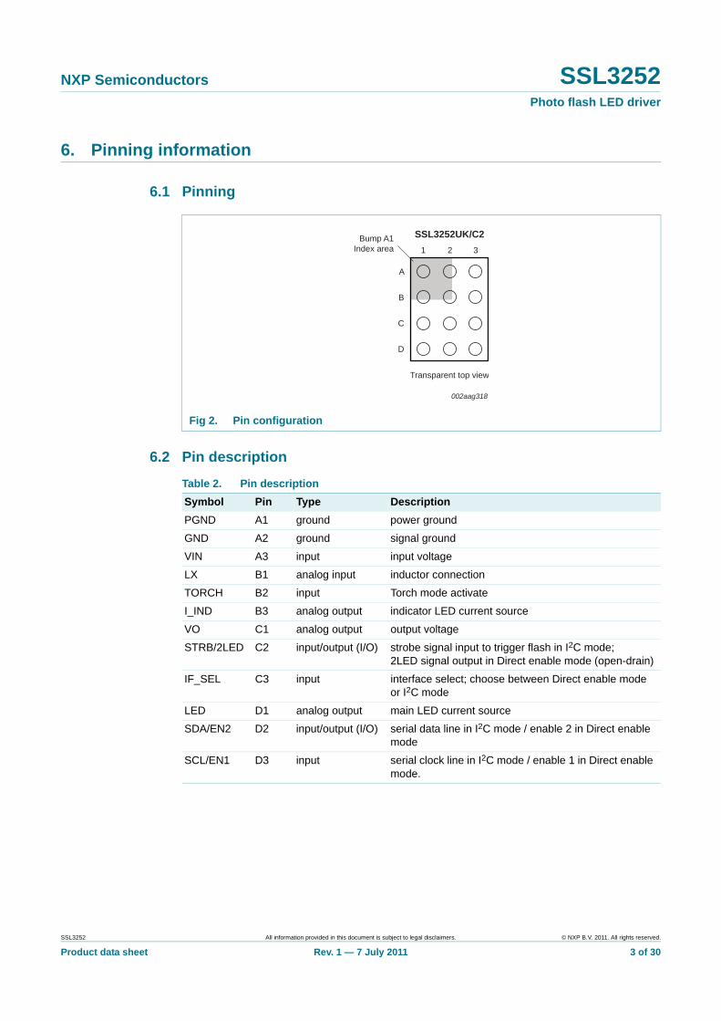
6. Pinning information
6.1 Pinning
6.2 Pin description
Fig 2. Pin configuration
1 2 3
A
B
C
D
SSL3252UK/C2Bump A1Index area
Transparent top view
002aag318
Table 2. Pin description
Symbol Pin Type Description
PGND A1 ground power ground
GND A2 ground signal ground
VIN A3 input input voltage
LX B1 analog input inductor connection
TORCH B2 input Torch mode activate
I_IND B3 analog output indicator LED current source
VO C1 analog output output voltage
STRB/2LED C2 input/output (I/O) strobe signal input to trigger flash in I2C mode; 2LED signal output in Direct enable mode (open-drain)
IF_SEL C3 input interface select; choose between Direct enable mode or I2C mode
LED D1 analog output main LED current source
SDA/EN2 D2 input/output (I/O) serial data line in I2C mode / enable 2 in Direct enable mode
SCL/EN1 D3 input serial clock line in I2C mode / enable 1 in Direct enable mode.
SSL3252 All information provided in this document is subject to legal disclaimers. © NXP B.V. 2011. All rights reserved.
Product data sheet Rev. 1 — 7 July 2011 3 of 30
NXP Semiconductors SSL3252Photo flash LED driver
7. Functional description
7.1 Introduction
The SSL3252 is a boost converter intended to drive either a single high power flash LED or two high power flash LEDs in series. The LED current is controlled by the output voltage of the boost converter and the integrated linear current source. The SSL3252 has two interface modes and six operational modes. The interface mode is selected by the interface select pin IF_SEL. Depending on the Interface mode selected, the device can either be controlled by an I2C-bus interface, or external enable lines.
The interface modes are:
• I2C mode
• Direct enable mode
The operational modes are:
• Standby mode
• Shut-down mode
• Flash mode
• Torch mode
• Assist light mode
• Indicator mode
In all LED modes, to ensure a constant switching frequency, the regulated converter employs Pulse Width Modulation (PWM).
In applications where the required LED voltage is lower than the applied input voltage, the converter switches to linear mode. The excess voltage difference between the required LED voltage and input voltage is now compensated by increasing the voltage over the linear current source and therefore on the LED pin.
Apart from the main LED(s), a separate indicator LED can be driven from the SSL3252. This is driven by a linear current source circuit that operates independent of the switch mode converter for the main LED(s).
7.2 Interface modes
The device is equipped with two interfaces: I2C and Direct enable. Which interface mode is used is defined by the level of the IF_SEL pin. Table 3 describes the interface possibilities.
Table 3. Interface modes
IF_SEL Interface mode Relevant controls
1 I2C mode SDA, SCL, STRB/2LED, TORCH
0 Direct enable mode EN1, EN2, TORCH
SSL3252 All information provided in this document is subject to legal disclaimers. © NXP B.V. 2011. All rights reserved.
Product data sheet Rev. 1 — 7 July 2011 4 of 30
NXP Semiconductors SSL3252Photo flash LED driver
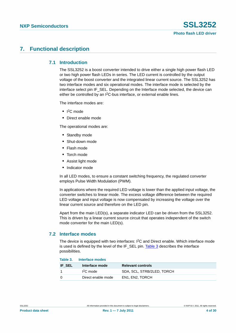
7.2.1 Using the direct enable control
When the Direct enable mode is used, the device can be switched to the various operational modes using the TORCH, EN1 and EN2 control signals. The definitions of these control signals are given in Table 4. The EN1 and EN2 functions of the SCL/EN1 and SDA/EN2 pins have a higher priority than the pin TORCH. Figure 3 shows all the possible transitions between the various interface modes.
The device is in Shut-down mode when all control pins (IF_SEL, EN1, EN2, TORCH) are LOW.
[1] X = Don’t care.
Fig 3. Direct enable mode transitions
Table 4. Direct enable logic definition
IF_SEL pin
SCL/EN1 pin
SDA/EN2 pin
TORCH pin
Mode Output states
0 0 0 0 Shut-down Outputs disabled; shut-down current less than 1 A
0 0 0 1 Torch Fixed value; 40 mA dual LEDs; 80 mA single LED
0 0 1 X[1] Assist light Fixed value; 40 mA dual LEDs; 80 mA single LED
0 1 0 X[1] Indicator Fixed value 2.5 mA
0 1 1 X[1] Flash Fixed value; 320 mA dual LEDs; 500 mA single LED
Shut-downmode
Indicatormode
Flashmode
Assist lightmode
Torchmode
014aaa303
SSL3252 All information provided in this document is subject to legal disclaimers. © NXP B.V. 2011. All rights reserved.
Product data sheet Rev. 1 — 7 July 2011 5 of 30
NXP Semiconductors SSL3252Photo flash LED driver
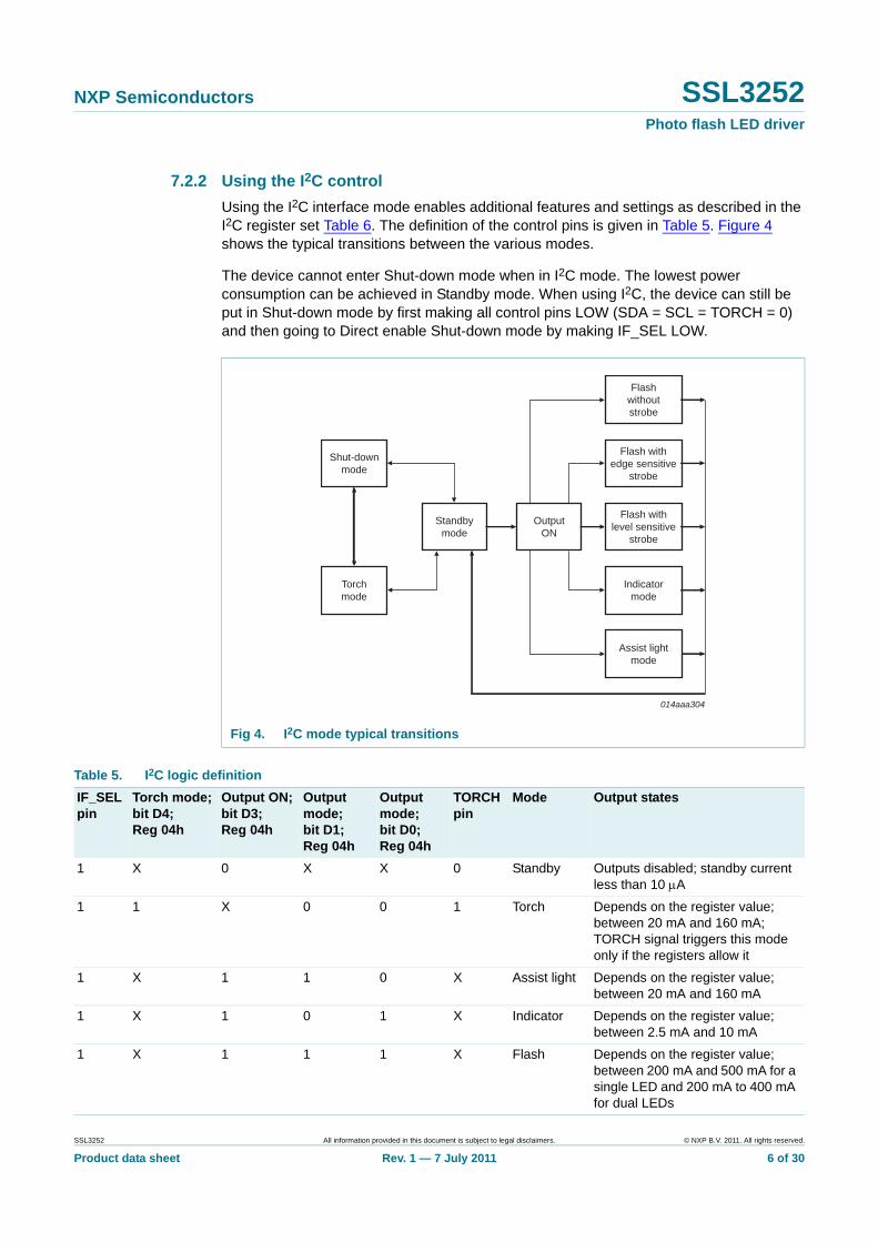
7.2.2 Using the I2C control
Using the I2C interface mode enables additional features and settings as described in the I2C register set Table 6. The definition of the control pins is given in Table 5. Figure 4 shows the typical transitions between the various modes.
The device cannot enter Shut-down mode when in I2C mode. The lowest power consumption can be achieved in Standby mode. When using I2C, the device can still be put in Shut-down mode by first making all control pins LOW (SDA = SCL = TORCH = 0) and then going to Direct enable Shut-down mode by making IF_SEL LOW.
Fig 4. I2C mode typical transitions
Indicatormode
Torchmode
Assist lightmode
OutputON
Standbymode
Flash withedge sensitive
strobe
Shut-downmode
Flashwithoutstrobe
Flash withlevel sensitive
strobe
014aaa304
Table 5. I2C logic definition
IF_SEL pin
Torch mode; bit D4; Reg 04h
Output ON; bit D3; Reg 04h
Output mode; bit D1; Reg 04h
Output mode; bit D0; Reg 04h
TORCH pin
Mode Output states
1 X 0 X X 0 Standby Outputs disabled; standby current less than 10 A
1 1 X 0 0 1 Torch Depends on the register value; between 20 mA and 160 mA; TORCH signal triggers this mode only if the registers allow it
1 X 1 1 0 X Assist light Depends on the register value; between 20 mA and 160 mA
1 X 1 0 1 X Indicator Depends on the register value; between 2.5 mA and 10 mA
1 X 1 1 1 X Flash Depends on the register value; between 200 mA and 500 mA for a single LED and 200 mA to 400 mA for dual LEDs
SSL3252 All information provided in this document is subject to legal disclaimers. © NXP B.V. 2011. All rights reserved.
Product data sheet Rev. 1 — 7 July 2011 6 of 30
NXP Semiconductors SSL3252Photo flash LED driver
7.3 Operational modes
7.3.1 Shut-down mode
To enter the Shut-down mode, all control pins, IF_SEL, EN1 function of SCL/EN1, EN2 function of SDA/EN2, and TORCH, must be LOW. In this mode, the internal circuitry of the device is turned off to guarantee a shut-down current of less than 1 A. The PMOS switch of the converter is conducting, and the NMOS is set to high-impedance. To avoid current leakage into the LED, the current source circuitry for both the main LED and the indicator LED are switched to high-impedance.
7.3.2 Standby mode
The device only enters Standby mode in I2C mode when pin IF_SEL is HIGH and the outputs are not active. In Standby mode, part of the internal circuitry of the device remains on, but the converter is not switching. To avoid current leakage into the LED, the current source circuitry for both the main LED and the indicator LED are switched to high-impedance. In this mode, I2C communication with the device is possible.
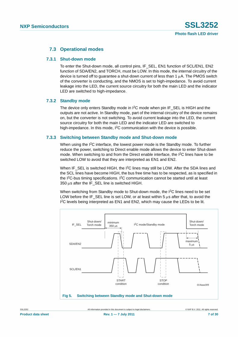
7.3.3 Switching between Standby mode and Shut-down mode
When using the I2C interface, the lowest power mode is the Standby mode. To further reduce the power, switching to Direct enable mode allows the device to enter Shut-down mode. When switching to and from the Direct enable interface, the I2C lines have to be switched LOW to avoid that they are interpreted as EN1 and EN2.
When IF_SEL is switched HIGH, the I2C lines may still be LOW. After the SDA lines and the SCL lines have become HIGH, the bus free time has to be respected, as is specified in the I2C-bus timing specifications. I2C communication cannot be started until at least 350 s after the IF_SEL line is switched HIGH.
When switching from Standby mode to Shut-down mode, the I2C lines need to be set LOW before the IF_SEL line is set LOW, or at least within 5 s after that, to avoid the I2C levels being interpreted as EN1 and EN2, which may cause the LEDs to be lit.
Fig 5. Switching between Standby mode and Shut-down mode
IF_SEL
SDA/EN2
SCL/EN1
STARTcondition
STOPcondition
minimum350 µs
maximum5 µs
I2C mode/Standby modeShut-down/Torch mode
Shut-down/Torch mode
014aaa305
SSL3252 All information provided in this document is subject to legal disclaimers. © NXP B.V. 2011. All rights reserved.
Product data sheet Rev. 1 — 7 July 2011 7 of 30
NXP Semiconductors SSL3252Photo flash LED driver
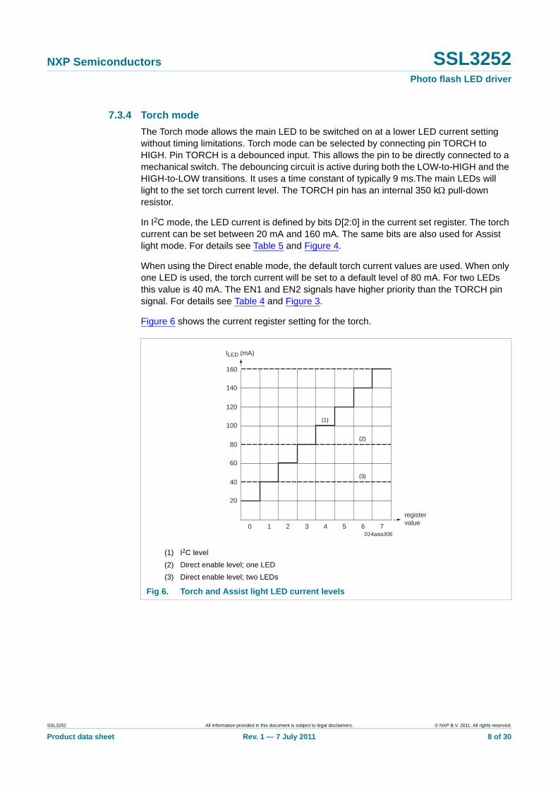
7.3.4 Torch mode
The Torch mode allows the main LED to be switched on at a lower LED current setting without timing limitations. Torch mode can be selected by connecting pin TORCH to HIGH. Pin TORCH is a debounced input. This allows the pin to be directly connected to a mechanical switch. The debouncing circuit is active during both the LOW-to-HIGH and the HIGH-to-LOW transitions. It uses a time constant of typically 9 ms.The main LEDs will light to the set torch current level. The TORCH pin has an internal 350 k pull-down resistor.
In I2C mode, the LED current is defined by bits D[2:0] in the current set register. The torch current can be set between 20 mA and 160 mA. The same bits are also used for Assist light mode. For details see Table 5 and Figure 4.
When using the Direct enable mode, the default torch current values are used. When only one LED is used, the torch current will be set to a default level of 80 mA. For two LEDs this value is 40 mA. The EN1 and EN2 signals have higher priority than the TORCH pin signal. For details see Table 4 and Figure 3.
Figure 6 shows the current register setting for the torch.
(1) I2C level
(2) Direct enable level; one LED
(3) Direct enable level; two LEDs
Fig 6. Torch and Assist light LED current levels
registervalue0 751 3 62 4
014aaa306
80
40
120
160
60
20
100
140
ILED (mA)
(1)
(2)
(3)
SSL3252 All information provided in this document is subject to legal disclaimers. © NXP B.V. 2011. All rights reserved.
Product data sheet Rev. 1 — 7 July 2011 8 of 30
NXP Semiconductors SSL3252Photo flash LED driver
7.3.5 Assist light mode
The Assist light mode allows the main LED to be switched on at a lower LED current setting, without any timing limitations. The Assist light mode can be selected in both I2C and Direct enable modes.
In I2C mode, the LED current is defined by bits D[2:0] in the current set register. The Assist light current value can be set between 20 mA and 160 mA. The same bits are also used for Torch mode. Entering Assist light mode is possible if bits D[1:0] from the control register are set to 10 and bit D3 from the same register is set to 1.
When using the Direct enable mode, the default Assist light current values are used. When only one LED is used, the Assist light current will be set to a default level of 80 mA. For two LEDs this value is 40 mA. The state of the EN1 function of the SCL/EN1 pin must be LOW and the state of the EN2 function of the SDA/EN2 pin HIGH to enter Assist light mode (see Table 4). Figure 6 shows the current register setting for the Assist light.
7.3.6 Flash mode
The Flash mode allows the main LEDs to be used at high current settings. The Flash mode current can be set to up to 500 mA in both the I2C mode and Direct enable mode.
In I2C mode, the current is defined by bits D[7:4] in the current set register. When two LEDs are used and the register is set for more than 400 mA, the maximum current is clipped to 400 mA. Generating the Flash mode can be done in the following three ways:
• software controlled
• edge sensitive strobe
• level sensitive strobe
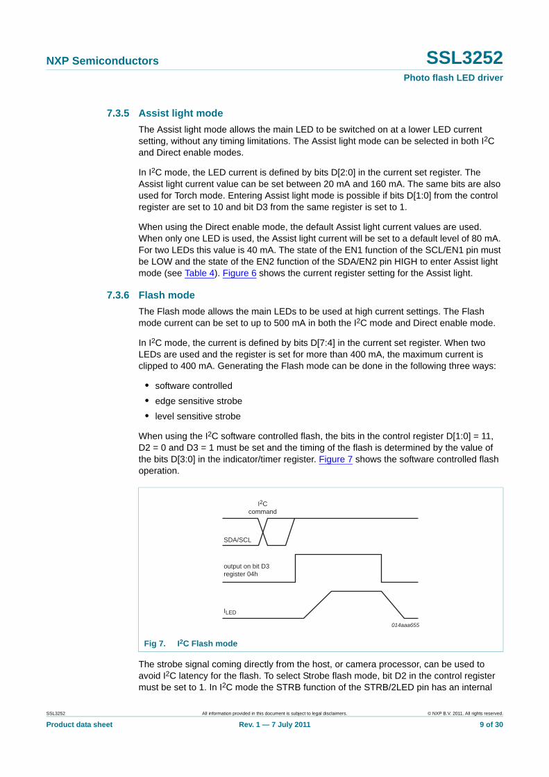
When using the I2C software controlled flash, the bits in the control register D[1:0] = 11, D2 = 0 and D3 = 1 must be set and the timing of the flash is determined by the value of the bits D[3:0] in the indicator/timer register. Figure 7 shows the software controlled flash operation.
The strobe signal coming directly from the host, or camera processor, can be used to avoid I2C latency for the flash. To select Strobe flash mode, bit D2 in the control register must be set to 1. In I2C mode the STRB function of the STRB/2LED pin has an internal
Fig 7. I2C Flash mode
014aaa655
output on bit D3 register 04h
I2Ccommand
SDA/SCL
ILED
SSL3252 All information provided in this document is subject to legal disclaimers. © NXP B.V. 2011. All rights reserved.
Product data sheet Rev. 1 — 7 July 2011 9 of 30
NXP Semiconductors SSL3252Photo flash LED driver
pull-down resistor of 350 k, and can be either level sensitive or edge sensitive, depending on the value of the bit D5 in the control register (0 = edge sensitive, 1 = level sensitive).
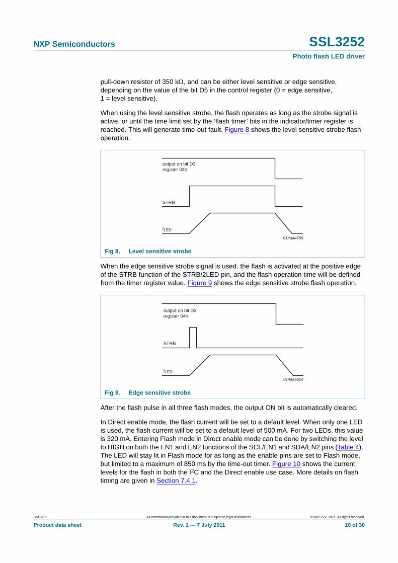
When using the level sensitive strobe, the flash operates as long as the strobe signal is active, or until the time limit set by the ‘flash timer’ bits in the indicator/timer register is reached. This will generate time-out fault. Figure 8 shows the level sensitive strobe flash operation.
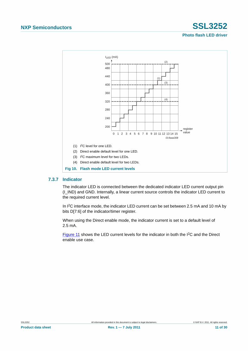
When the edge sensitive strobe signal is used, the flash is activated at the positive edge of the STRB function of the STRB/2LED pin, and the flash operation time will be defined from the timer register value. Figure 9 shows the edge sensitive strobe flash operation.
After the flash pulse in all three flash modes, the output ON bit is automatically cleared.
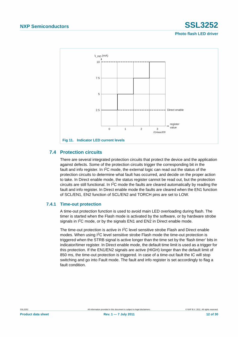
In Direct enable mode, the flash current will be set to a default level. When only one LED is used, the flash current will be set to a default level of 500 mA. For two LEDs, this value is 320 mA. Entering Flash mode in Direct enable mode can be done by switching the level to HIGH on both the EN1 and EN2 functions of the SCL/EN1 and SDA/EN2 pins (Table 4). The LED will stay lit in Flash mode for as long as the enable pins are set to Flash mode, but limited to a maximum of 850 ms by the time-out timer. Figure 10 shows the current levels for the flash in both the I2C and the Direct enable use case. More details on flash timing are given in Section 7.4.1.
Fig 8. Level sensitive strobe
Fig 9. Edge sensitive strobe
014aaa656
output on bit D3register 04h
STRB
ILED
014aaa654
output on bit D3 register 04h
STRB
ILED
SSL3252 All information provided in this document is subject to legal disclaimers. © NXP B.V. 2011. All rights reserved.
Product data sheet Rev. 1 — 7 July 2011 10 of 30
NXP Semiconductors SSL3252Photo flash LED driver
7.3.7 Indicator
The indicator LED is connected between the dedicated indicator LED current output pin (I_IND) and GND. Internally, a linear current source controls the indicator LED current to the required current level.
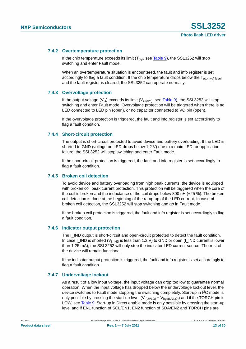
In I2C interface mode, the indicator LED current can be set between 2.5 mA and 10 mA by bits D[7:6] of the indicator/timer register.
When using the Direct enable mode, the indicator current is set to a default level of 2.5 mA.
Figure 11 shows the LED current levels for the indicator in both the I2C and the Direct enable use case.
(1) I2C level for one LED.
(2) Direct enable default level for one LED.
(3) I2C maximum level for two LEDs.
(4) Direct enable default level for two LEDs.
Fig 10. Flash mode LED current levels
registervalue0 14128 102 4 6 13 15117 91 3 5
014aaa308
280
240
320
400
360
440
480500
ILED (mA)
200
(1)
(2)
(3)
(4)
SSL3252 All information provided in this document is subject to legal disclaimers. © NXP B.V. 2011. All rights reserved.
Product data sheet Rev. 1 — 7 July 2011 11 of 30
NXP Semiconductors SSL3252Photo flash LED driver
7.4 Protection circuits
There are several integrated protection circuits that protect the device and the application against defects. Some of the protection circuits trigger the corresponding bit in the fault and info register. In I2C mode, the external logic can read out the status of the protection circuits to determine what fault has occurred, and decide on the proper action to take. In Direct enable mode, the status register cannot be read out, but the protection circuits are still functional. In I2C mode the faults are cleared automatically by reading the fault and info register. In Direct enable mode the faults are cleared when the EN1 function of SCL/EN1, EN2 function of SCL/EN2 and TORCH pins are set to LOW.
7.4.1 Time-out protection
A time-out protection function is used to avoid main LED overloading during flash. The timer is started when the Flash mode is activated by the software, or by hardware strobe signals in I2C mode, or by the signals EN1 and EN2 in Direct enable mode.
The time-out protection is active in I2C level sensitive strobe Flash and Direct enable modes. When using I2C level sensitive strobe Flash mode the time-out protection is triggered when the STRB signal is active longer than the time set by the ‘flash timer’ bits in indicator/timer register. In Direct enable mode, the default time limit is used as a trigger for this protection. If the EN1/EN2 signals are active (HIGH) longer than the default limit of 850 ms, the time-out protection is triggered. In case of a time-out fault the IC will stop switching and go into Fault mode. The fault and info register is set accordingly to flag a fault condition.
Fig 11. Indicator LED current levels
registervalue0 31 2
014aaa309
5
2.5
7.5
10
II_IND (mA)
Direct enable
SSL3252 All information provided in this document is subject to legal disclaimers. © NXP B.V. 2011. All rights reserved.
Product data sheet Rev. 1 — 7 July 2011 12 of 30
NXP Semiconductors SSL3252Photo flash LED driver
7.4.2 Overtemperature protection
If the chip temperature exceeds its limit (Totp, see Table 9), the SSL3252 will stop switching and enter Fault mode.
When an overtemperature situation is encountered, the fault and info register is set accordingly to flag a fault condition. If the chip temperature drops below the Totp(hys) level and the fault register is cleared, the SSL3252 can operate normally.
7.4.3 Overvoltage protection
If the output voltage (VO) exceeds its limit (VO(ovp), see Table 9), the SSL3252 will stop switching and enter Fault mode. Overvoltage protection will be triggered when there is no LED connected to LED pin (open), or no capacitor connected to VO pin (open).
If the overvoltage protection is triggered, the fault and info register is set accordingly to flag a fault condition.
7.4.4 Short-circuit protection
The output is short-circuit protected to avoid device and battery overloading. If the LED is shorted to GND (voltage on LED drops below 1.2 V) due to a main LED, or application failure, the SSL3252 will stop switching and enter Fault mode.
If the short-circuit protection is triggered, the fault and info register is set accordingly to flag a fault condition.
7.4.5 Broken coil detection
To avoid device and battery overloading from high peak currents, the device is equipped with broken coil peak current protection. This protection will be triggered when the core of the coil is broken and the inductance of the coil drops below 800 nH (25 %). The broken coil detection is done at the beginning of the ramp-up of the LED current. In case of broken coil detection, the SSL3252 will stop switching and go in Fault mode.
If the broken coil protection is triggered, the fault and info register is set accordingly to flag a fault condition.
7.4.6 Indicator output protection
The I_IND output is short-circuit and open-circuit protected to detect the fault condition. In case I_IND is shorted (VI_IND is less than 1.2 V) to GND or open (I_IND current is lower than 1.25 mA), the SSL3252 will only stop the indicator LED current source. The rest of the device will remain functional.
If the indicator output protection is triggered, the fault and info register is set accordingly to flag a fault condition.
7.4.7 Undervoltage lockout
As a result of a low input voltage, the input voltage can drop too low to guarantee normal operation. When the input voltage has dropped below the undervoltage lockout level, the device switches to Fault mode stopping the switching completely. Start-up in I2C mode is only possible by crossing the start-up level (VI(UVLO) + Vhys(UVLO)) and if the TORCH pin is LOW, see Table 9. Start-up in Direct enable mode is only possible by crossing the start-up level and if EN1 function of SCL/EN1, EN2 function of SDA/EN2 and TORCH pins are
SSL3252 All information provided in this document is subject to legal disclaimers. © NXP B.V. 2011. All rights reserved.
Product data sheet Rev. 1 — 7 July 2011 13 of 30
NXP Semiconductors SSL3252Photo flash LED driver
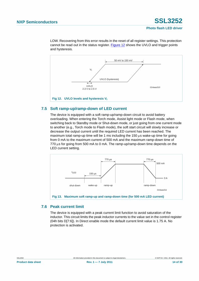
LOW. Recovering from this error results in the reset of all register settings. This protection cannot be read out in the status register. Figure 12 shows the UVLO and trigger points and hysteresis.
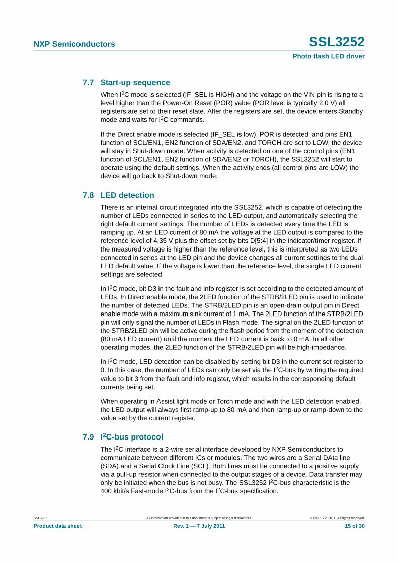
7.5 Soft ramp-up/ramp-down of LED current
The device is equipped with a soft ramp-up/ramp-down circuit to avoid battery overloading. When entering the Torch mode, Assist light mode or Flash mode, when switching back to Standby mode or Shut-down mode, or just going from one current mode to another (e.g., Torch mode to Flash mode), the soft start circuit will slowly increase or decrease the output current until the required LED current has been reached. The maximum total ramp-up time will be 1 ms including the 150 s wake-up time for going from 0 mA to the maximum current of 500 mA and the maximum ramp-down time of 770 s for going from 500 mA to 0 mA. The ramp-up/ramp-down time depends on the LED current setting.
7.6 Peak current limit
The device is equipped with a peak current limit function to avoid saturation of the inductor. This circuit limits the peak inductor currents to the value set in the control register (04h bits D[7:6]). In Direct enable mode the default current limit value is 1.75 A. No protection is activated.
Fig 12. UVLO levels and hysteresis VI
VI
UVLO2.3 V to 2.5 V
50 mV to 150 mV
UVLO (hysteresis)
014aaa310
Fig 13. Maximum soft ramp-up and ramp-down time (for 500 mA LED current)
770 µs
150 µs
770 µs
ILED
500 mA
0 A
ramp-downramp-up
014aaa311
shut-down wake-up
SSL3252 All information provided in this document is subject to legal disclaimers. © NXP B.V. 2011. All rights reserved.
Product data sheet Rev. 1 — 7 July 2011 14 of 30
NXP Semiconductors SSL3252Photo flash LED driver
7.7 Start-up sequence
When I2C mode is selected (IF_SEL is HIGH) and the voltage on the VIN pin is rising to a level higher than the Power-On Reset (POR) value (POR level is typically 2.0 V) all registers are set to their reset state. After the registers are set, the device enters Standby mode and waits for I2C commands.
If the Direct enable mode is selected (IF_SEL is low), POR is detected, and pins EN1 function of SCL/EN1, EN2 function of SDA/EN2, and TORCH are set to LOW, the device will stay in Shut-down mode. When activity is detected on one of the control pins (EN1 function of SCL/EN1, EN2 function of SDA/EN2 or TORCH), the SSL3252 will start to operate using the default settings. When the activity ends (all control pins are LOW) the device will go back to Shut-down mode.
7.8 LED detection
There is an internal circuit integrated into the SSL3252, which is capable of detecting the number of LEDs connected in series to the LED output, and automatically selecting the right default current settings. The number of LEDs is detected every time the LED is ramping up. At an LED current of 80 mA the voltage at the LED output is compared to the reference level of 4.35 V plus the offset set by bits D[5:4] in the indicator/timer register. If the measured voltage is higher than the reference level, this is interpreted as two LEDs connected in series at the LED pin and the device changes all current settings to the dual LED default value. If the voltage is lower than the reference level, the single LED current settings are selected.
In I2C mode, bit D3 in the fault and info register is set according to the detected amount of LEDs. In Direct enable mode, the 2LED function of the STRB/2LED pin is used to indicate the number of detected LEDs. The STRB/2LED pin is an open-drain output pin in Direct enable mode with a maximum sink current of 1 mA. The 2LED function of the STRB/2LED pin will only signal the number of LEDs in Flash mode. The signal on the 2LED function of the STRB/2LED pin will be active during the flash period from the moment of the detection (80 mA LED current) until the moment the LED current is back to 0 mA. In all other operating modes, the 2LED function of the STRB/2LED pin will be high-impedance.
In I2C mode, LED detection can be disabled by setting bit D3 in the current set register to 0. In this case, the number of LEDs can only be set via the I2C-bus by writing the required value to bit 3 from the fault and info register, which results in the corresponding default currents being set.
When operating in Assist light mode or Torch mode and with the LED detection enabled, the LED output will always first ramp-up to 80 mA and then ramp-up or ramp-down to the value set by the current register.
7.9 I2C-bus protocol
The I2C interface is a 2-wire serial interface developed by NXP Semiconductors to communicate between different ICs or modules. The two wires are a Serial DAta line (SDA) and a Serial Clock Line (SCL). Both lines must be connected to a positive supply via a pull-up resistor when connected to the output stages of a device. Data transfer may only be initiated when the bus is not busy. The SSL3252 I2C-bus characteristic is the 400 kbit/s Fast-mode I2C-bus from the I2C-bus specification.
SSL3252 All information provided in this document is subject to legal disclaimers. © NXP B.V. 2011. All rights reserved.
Product data sheet Rev. 1 — 7 July 2011 15 of 30
NXP Semiconductors SSL3252Photo flash LED driver
Remark: For more details on the I2C-bus standard, refer to the document UM10204, “I2C-bus specification and user manual” (www.nxp.com/documents/user_manual/UM10204.pdf).
The following text describes the protocols used by the SSL3252 for the read and write sequences. The read sequence may use a repeated START condition during the sequence, to stop the bus being released during the communication. The sequences can be used to read or write only one data byte, or to read or write a sequence of data bytes.
After a START condition, a valid hardware address must be sent to the SSL3252 followed by a subaddress and n data bytes. See Figure 14 and Figure 15 below. For the format and the timing of the START condition (S), the STOP condition (P) and the Acknowledge bit (A), refer to the user manual UM10204.
7.9.1 Addressing
Each SSL3252 in an I2C-bus system is activated by sending a valid slave address to the device. The slave address always has to be sent as the first byte after the START condition in the I2C-bus protocol. See Figure 16.
Fig 14. I2C write data transfer format
Fig 15. I2C read data transfer format
S slave address W A
from master to slave
from slave to master
subaddress n A
S = START conditionP = STOP conditionA = AcknowledgeN = Not Acknowledged
nth register A P
014aaa316
S slave address W A
S slave address R A
subaddress n A
nth register N P
from master to slave
from slave to master
S = START conditionP = STOP conditionA = AcknowledgeN = Not Acknowledged
014aaa317
Fig 16. I2C slave address
0 1 1 0 0 0 0 RW
MSB LSB
014aaa318
SSL3252 All information provided in this document is subject to legal disclaimers. © NXP B.V. 2011. All rights reserved.
Product data sheet Rev. 1 — 7 July 2011 16 of 30
NXP Semiconductors SSL3252Photo flash LED driver
There is one address byte required since 7-bit addresses are used. The last bit of the address byte is the read/write bit and should always be set according to the required operation. This 7-bit address is 0110 000b (30h). The combination with the LSB R/W bit gives a write address of 60h and a read address of 61h.
The second byte sent to the SSL3252 is the subaddress of the specific register.
7.9.2 Data
After the subaddress the data bytes are sent. The definition of the data transfer is given in Figure 14 and Figure 15. After each data byte an acknowledge is given and the subaddress is automatically incremented to the next subaddress.
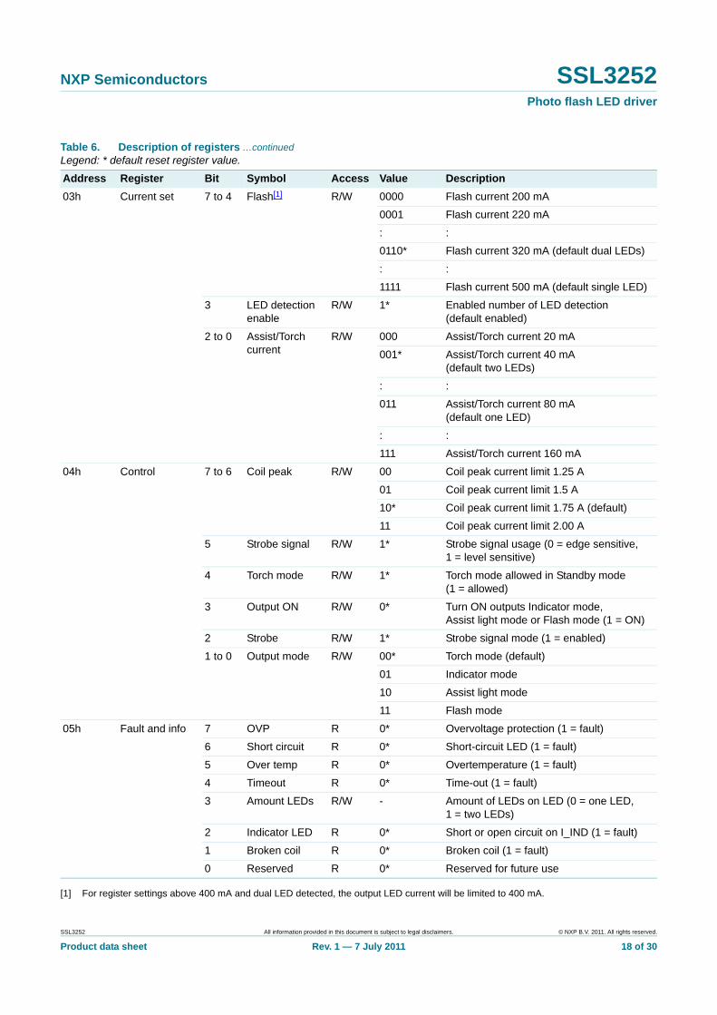
A description of the data that can be programmed in the registers is given in Table 6.
7.9.3 Register map
Table 6. Description of registersLegend: * default reset register value.
Address Register Bit Symbol Access Value Description
00h Design info 7 to 4 Man_ID R 0100* Manufacturer ID
3 to 0 Model_ID R 0001* Model ID
01h Version control 7 to 4 Reserved R 0000* Reserved for future use
3 to 0 Design version R 0000 Design version 1
0001 Design version 2
: :
1111 Design version 16
02h Indicator/timer 7 to 6 Indicator current
R/W 00* Indicator LED current 2.5 mA (default)
01 Indicator LED current 5 mA
10 Indicator LED current 7.5 mA
11 Indicator LED current 10 mA
5 to 4 Vref offset R/W 00* No offset (default)
01 Offset = Vref + 0.3 V
10 Offset = Vref 0.3 V
11 Offset = Vref + 0.6 V
3 to 0 Flash timer R/W 0000 Software flash timer value 100 ms
0001 Software flash timer value 150 ms
: :
1111* Software flash timer value 850 ms (default)
SSL3252 All information provided in this document is subject to legal disclaimers. © NXP B.V. 2011. All rights reserved.
Product data sheet Rev. 1 — 7 July 2011 17 of 30
NXP Semiconductors SSL3252Photo flash LED driver
[1] For register settings above 400 mA and dual LED detected, the output LED current will be limited to 400 mA.
03h Current set 7 to 4 Flash[1] R/W 0000 Flash current 200 mA
0001 Flash current 220 mA
: :
0110* Flash current 320 mA (default dual LEDs)
: :
1111 Flash current 500 mA (default single LED)
3 LED detection enable
R/W 1* Enabled number of LED detection (default enabled)
2 to 0 Assist/Torch current
R/W 000 Assist/Torch current 20 mA
001* Assist/Torch current 40 mA (default two LEDs)
: :
011 Assist/Torch current 80 mA (default one LED)
: :
111 Assist/Torch current 160 mA
04h Control 7 to 6 Coil peak R/W 00 Coil peak current limit 1.25 A
01 Coil peak current limit 1.5 A
10* Coil peak current limit 1.75 A (default)
11 Coil peak current limit 2.00 A
5 Strobe signal R/W 1* Strobe signal usage (0 = edge sensitive, 1 = level sensitive)
4 Torch mode R/W 1* Torch mode allowed in Standby mode (1 = allowed)
3 Output ON R/W 0* Turn ON outputs Indicator mode, Assist light mode or Flash mode (1 = ON)
2 Strobe R/W 1* Strobe signal mode (1 = enabled)
1 to 0 Output mode R/W 00* Torch mode (default)
01 Indicator mode
10 Assist light mode
11 Flash mode
05h Fault and info 7 OVP R 0* Overvoltage protection (1 = fault)
6 Short circuit R 0* Short-circuit LED (1 = fault)
5 Over temp R 0* Overtemperature (1 = fault)
4 Timeout R 0* Time-out (1 = fault)
3 Amount LEDs R/W - Amount of LEDs on LED (0 = one LED, 1 = two LEDs)
2 Indicator LED R 0* Short or open circuit on I_IND (1 = fault)
1 Broken coil R 0* Broken coil (1 = fault)
0 Reserved R 0* Reserved for future use
Table 6. Description of registers …continuedLegend: * default reset register value.
Address Register Bit Symbol Access Value Description
SSL3252 All information provided in this document is subject to legal disclaimers. © NXP B.V. 2011. All rights reserved.
Product data sheet Rev. 1 — 7 July 2011 18 of 30
NXP Semiconductors SSL3252Photo flash LED driver
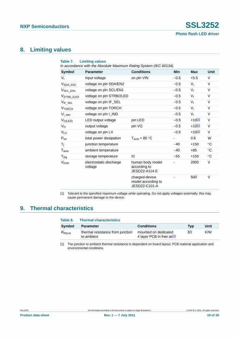
8. Limiting values
[1] Tolerant to the specified maximum voltage while operating. Do not apply voltages externally; this may cause permanent damage to the device.
9. Thermal characteristics
[1] The junction to ambient thermal resistance is dependent on board layout, PCB material application and environmental conditions.
Table 7. Limiting valuesIn accordance with the Absolute Maximum Rating System (IEC 60134).
Symbol Parameter Conditions Min Max Unit
VI input voltage on pin VIN 0.5 +5.5 V
VSDA_EN2 voltage on pin SDA/EN2 0.5 VI V
VSCL_EN1 voltage on pin SCL/EN1 0.5 VI V
VSTRB_2LED voltage on pin STRB/2LED 0.5 VI V
VIF_SEL voltage on pin IF_SEL 0.5 VI V
VTORCH voltage on pin TORCH 0.5 VI V
VI_IND voltage on pin I_IND 0.5 VI V
VO(LED) LED output voltage pin LED 0.5 +10[1] V
VO output voltage pin VO 0.5 +10[1] V
VLX voltage on pin LX 0.5 +10[1] V
Ptot total power dissipation Tamb = 85 C - 0.8 W
Tj junction temperature 40 +150 C
Tamb ambient temperature 40 +85 C
Tstg storage temperature IC 55 +150 C
VESD electrostatic discharge voltage
human body model according to JESD22-A114-E
- 2000 V
charged-device model according to JESD22-C101-A
- 500 V
Table 8. Thermal characteristics
Symbol Parameter Conditions Typ Unit
Rth(j-a) thermal resistance from junction to ambient
mounted on dedicated 4 layer PCB in free air[1]
83 K/W
SSL3252 All information provided in this document is subject to legal disclaimers. © NXP B.V. 2011. All rights reserved.
Product data sheet Rev. 1 — 7 July 2011 19 of 30
NXP Semiconductors SSL3252Photo flash LED driver
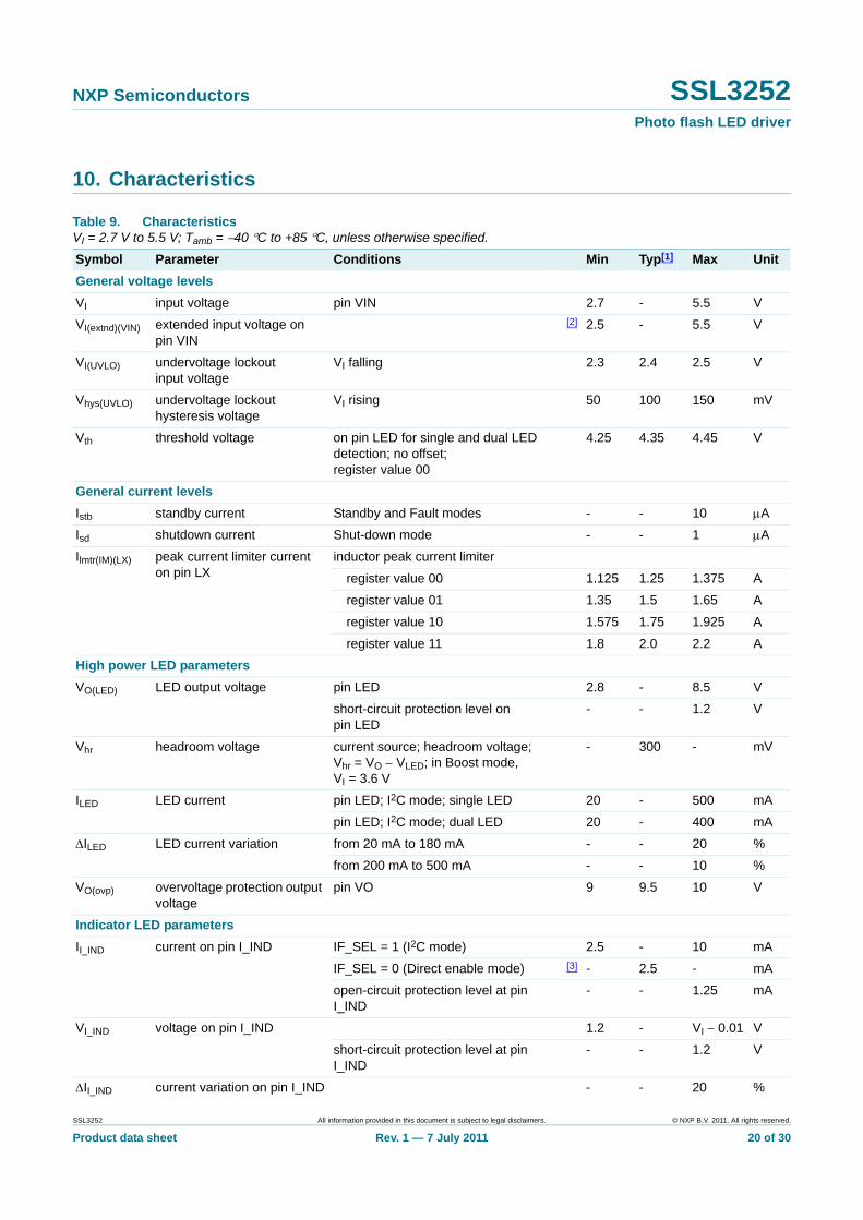
10. Characteristics
Table 9. CharacteristicsVI = 2.7 V to 5.5 V; Tamb = 40 C to +85 C, unless otherwise specified.
Symbol Parameter Conditions Min Typ[1] Max Unit
General voltage levels
VI input voltage pin VIN 2.7 - 5.5 V
VI(extnd)(VIN) extended input voltage on pin VIN
[2] 2.5 - 5.5 V
VI(UVLO) undervoltage lockout input voltage
VI falling 2.3 2.4 2.5 V
Vhys(UVLO) undervoltage lockout hysteresis voltage
VI rising 50 100 150 mV
Vth threshold voltage on pin LED for single and dual LED detection; no offset; register value 00
4.25 4.35 4.45 V
General current levels
Istb standby current Standby and Fault modes - - 10 A
Isd shutdown current Shut-down mode - - 1 A
Ilmtr(IM)(LX) peak current limiter current on pin LX
inductor peak current limiter
register value 00 1.125 1.25 1.375 A
register value 01 1.35 1.5 1.65 A
register value 10 1.575 1.75 1.925 A
register value 11 1.8 2.0 2.2 A
High power LED parameters
VO(LED) LED output voltage pin LED 2.8 - 8.5 V
short-circuit protection level on pin LED
- - 1.2 V
Vhr headroom voltage current source; headroom voltage; Vhr = VO VLED; in Boost mode, VI = 3.6 V
- 300 - mV
ILED LED current pin LED; I2C mode; single LED 20 - 500 mA
pin LED; I2C mode; dual LED 20 - 400 mA
ILED LED current variation from 20 mA to 180 mA - - 20 %
from 200 mA to 500 mA - - 10 %
VO(ovp) overvoltage protection output voltage
pin VO 9 9.5 10 V
Indicator LED parameters
II_IND current on pin I_IND IF_SEL = 1 (I2C mode) 2.5 - 10 mA
IF_SEL = 0 (Direct enable mode) [3] - 2.5 - mA
open-circuit protection level at pin I_IND
- - 1.25 mA
VI_IND voltage on pin I_IND 1.2 - VI 0.01 V
short-circuit protection level at pin I_IND
- - 1.2 V
II_IND current variation on pin I_IND - - 20 %
SSL3252 All information provided in this document is subject to legal disclaimers. © NXP B.V. 2011. All rights reserved.
Product data sheet Rev. 1 — 7 July 2011 20 of 30
NXP Semiconductors SSL3252Photo flash LED driver
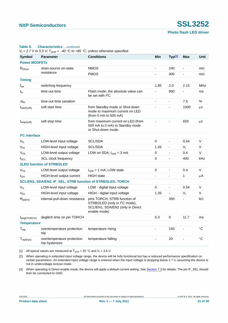
[1] All typical values are measured at Tamb = 25 C and VI = 3.6 V.
[2] When operating in extended input voltage range, the device will be fully functional but has a reduced performance specification on certain parameters. An extended input voltage range is entered when the input voltage is dropping below 2.7 V, assuming the device is not in undervoltage lockout mode.
[3] When operating in Direct enable mode, the device will apply a default current setting. See Section 7.3 for details. The pin IF_SEL should then be connected to GND.
Power MOSFETs
RDSon drain-source on-state resistance
NMOS - 240 - m
PMOS - 400 - m
Timing
fsw switching frequency 1.85 2.0 2.15 MHz
tto time-out time Flash mode; the absolute value can be set with I2C
- 850 - ms
tto time-out time variation - - 7.5 %
tstart(soft) soft start time from Standby mode or Shut-down mode to maximum current on LED (from 0 mA to 500 mA)
- - 1000 s
tstop(soft) soft stop time from maximum current on LED (from 500 mA to 0 mA) to Standby mode or Shut-down mode
- - 825 s
I2C interface
VIL LOW-level input voltage SCL/SDA 0 - 0.54 V
VIH HIGH-level input voltage SCL/SDA 1.26 - VI V
VOL LOW-level output voltage LOW on SDA; Isink = 3 mA 0 - 0.4 V
fSCL SCL clock frequency 0 - 400 kHz
2LED function of STRB/2LED
VOL LOW-level output voltage Isink = 1 mA; LOW state 0 - 0.4 V
IOH HIGH-level output current HIGH state - - 1 A
SCL/EN1, SDA/EN2, IF_SEL, STRB function of STRB/2LED, TORCH
VIL LOW-level input voltage LOW - digital input voltage 0 - 0.54 V
VIH HIGH-level input voltage HIGH - digital input voltage 1.26 - VI V
Rpd(int) internal pull-down resistance pins TORCH, STRB function of STRB/2LED (only in I2C mode), SCL/EN1, SDA/EN2 (only in Direct enable mode)
- 350 - k
tdegl(TORCH) deglitch time on pin TORCH 6.3 9 11.7 ms
Temperature
Totp overtemperature protection trip
temperature rising - 150 - C
Totp(hys) overtemperature protection trip hysteresis
temperature falling - 20 - C
Table 9. Characteristics …continuedVI = 2.7 V to 5.5 V; Tamb = 40 C to +85 C, unless otherwise specified.
Symbol Parameter Conditions Min Typ[1] Max Unit
SSL3252 All information provided in this document is subject to legal disclaimers. © NXP B.V. 2011. All rights reserved.
Product data sheet Rev. 1 — 7 July 2011 21 of 30
NXP Semiconductors SSL3252Photo flash LED driver
11. Application information
11.1 Input capacitor
For good input voltage decoupling, a low ESR ceramic capacitor is highly recommended. A 4.7 F (X5R/X7R) 6.3 V is the minimum recommended value. Since the input capacitor is supplying the input ripple current, a larger capacitor will improve both the transient behavior of the regulator and the EMI behavior of the power supply. Taking capacitor DC bias and temperature de-rating specifications into account, a 10 F (X5R/X7R) is preferred. Although increasing component count, a smaller capacitor of 100 nF (X5R/X7R) placed in parallel to the input capacitor will also improve EMI behavior.
11.2 Output capacitor
The output capacitor supplies the current into the main LED, while the inductor is being charged, and it also ensures loop stability. The minimum capacitance for stable loop operation would be 4.7 F, but taking capacitor DC bias and temperature de-rating specifications into account, a low ESR ceramic capacitor of 10 F (X5R/X7R) is highly recommended. A higher value of capacitance will improve output current ripple, while maintaining loop stability. Typically the SSL3252 overvoltage limit on pin VO is at 9.5 V, and the rated voltage of the output capacitor should be at least 10 V.
11.3 Inductor
The device has been designed to operate well with inductance values between 1.5 H and 3.3 H, in order to optimize for solution size. In a typical high current dual flash LED application a 2.2 H inductance is recommended. The inductor’s saturation current should be greater than or equal to the inductor peak current limiter current, which is a typical 1.75 A. During normal operation, it is recommended to keep the inductor peak current below this value. The copper losses and magnetic hysteresis losses in the inductor also contribute to the total system losses.
11.4 PCB layout
It is essential to have a good circuit layout in order to maximize efficiency and minimize EMI disturbance. The circuit topology uses an inductor, which is often seen as a main source of EMI disturbance, but any loop of wire carrying a current is essentially an electromagnet, whose field strength is proportional to the current. Careful circuit layout is therefore very important, keeping loop areas small and minimizing the magnetic flux. Due to the way a boost converter operates, there are two power states. One state when the internal NMOS switch is ON, and one when the NMOS switch is OFF. During each state there will be a current loop made by the power components that are conducting. The input and output capacitors must be arranged in such a way on the SSL3252 that during each of the two states the current loop is conducting in the same direction. This prevents phase reversal of the magnetic field, and reduces radiated EMI. The current loop area should be kept small by placing the power components as close as possible to the SSL3252. Use ground planes to keep the loop areas to a minimum.
SSL3252 All information provided in this document is subject to legal disclaimers. © NXP B.V. 2011. All rights reserved.
Product data sheet Rev. 1 — 7 July 2011 22 of 30
NXP Semiconductors SSL3252Photo flash LED driver
Priority should be given for the output capacitor to be positioned as close as possible to the VO and PGND nodes of the SSL3252. Since large currents will flow from input capacitor to the inductor and not to the VIN pin of the SSL3252, it is wise to locate the input capacitor near the inductor. The VIN pin should be star-connected to the positive pad of the input capacitor.
PGND and GND of the SSL3252 should be directly connected to each other. Place the ground connection of the output capacitor as close as possible to the PGND pin of the SSL3252.
The preferred minimum trace width for the high current width is 15 mm/A.
SSL3252 All information provided in this document is subject to legal disclaimers. © NXP B.V. 2011. All rights reserved.
Product data sheet Rev. 1 — 7 July 2011 23 of 30
NXP Semiconductors SSL3252Photo flash LED driver
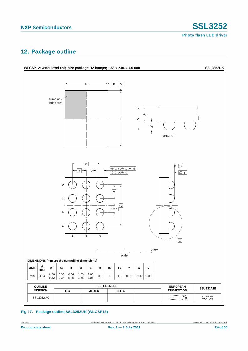
12. Package outline
Fig 17. Package outline SSL3252UK (WLCSP12)
REFERENCESOUTLINEVERSION
EUROPEANPROJECTION
ISSUE DATEIEC JEDEC JEITA
SSL3252UK
SSL3252UK
07-11-1907-11-23
UNIT Amax
mm 0.64 0.260.22
0.380.34
1.601.55
2.082.03 0.5 1 0.01 0.04
A1
DIMENSIONS (mm are the controlling dimensions)
WLCSP12: wafer level chip-size package; 12 bumps; 1.58 x 2.06 x 0.6 mm
0 1 2 mm
scale
A2 b
0.340.30
D E e e1 e2
1.5
v w y
0.02
bump A1index area
B AD
E
b
e2
e1
e
e
1/2 e
AC B∅ v M
C∅ w M
D
A
321
B
C
detail X
A
A2
A1
C
y
X
SSL3252 All information provided in this document is subject to legal disclaimers. © NXP B.V. 2011. All rights reserved.
Product data sheet Rev. 1 — 7 July 2011 24 of 30
NXP Semiconductors SSL3252Photo flash LED driver
13. Soldering of WLCSP packages
13.1 Introduction to soldering WLCSP packages
This text provides a very brief insight into a complex technology. A more in-depth account of soldering WLCSP (Wafer Level Chip-Size Packages) can be found in application note AN10439 “Wafer Level Chip Scale Package” and in application note AN10365 “Surface mount reflow soldering description”.
Wave soldering is not suitable for this package.
All NXP WLCSP packages are lead-free.
13.2 Board mounting
Board mounting of a WLCSP requires several steps:
1. Solder paste printing on the PCB
2. Component placement with a pick and place machine
3. The reflow soldering itself
13.3 Reflow soldering
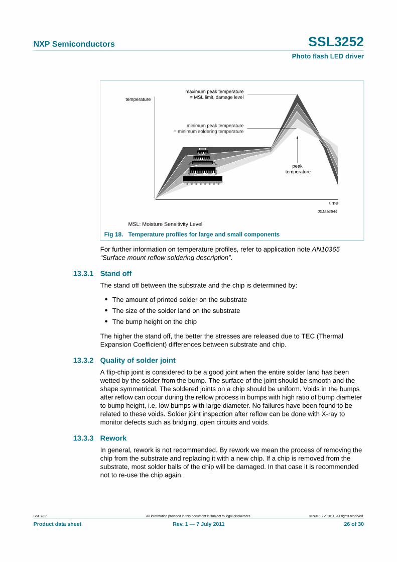
Key characteristics in reflow soldering are:
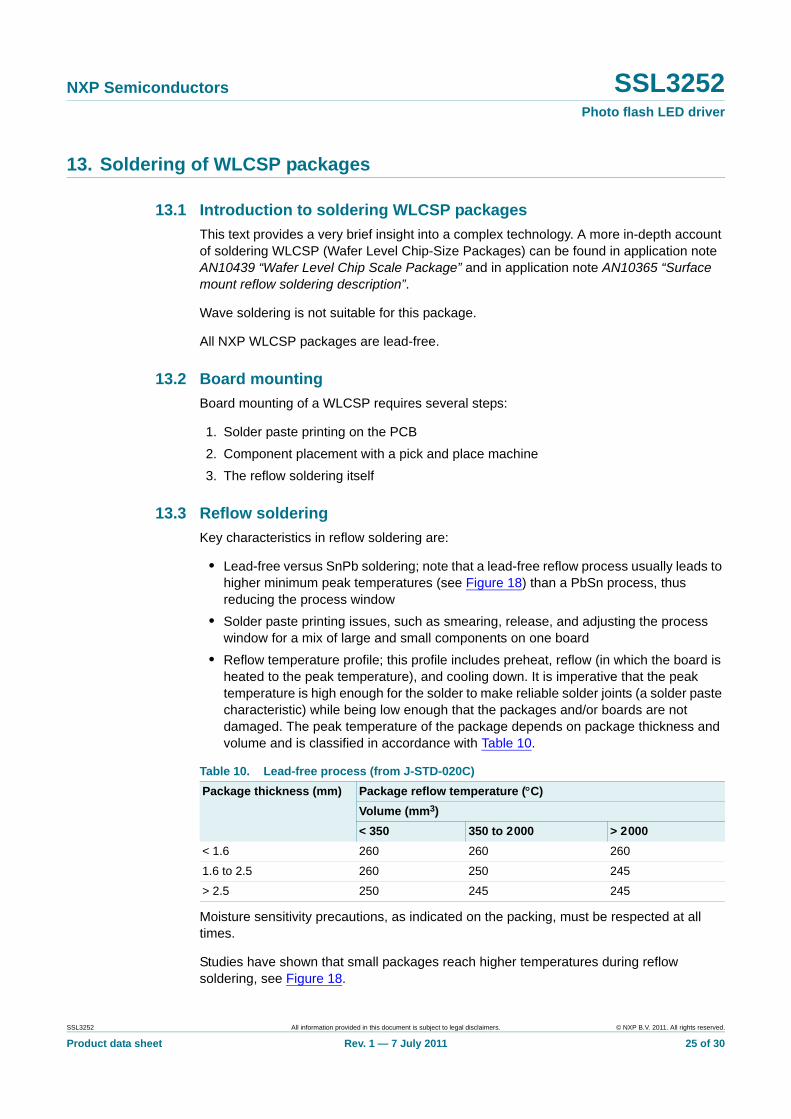
• Lead-free versus SnPb soldering; note that a lead-free reflow process usually leads to higher minimum peak temperatures (see Figure 18) than a PbSn process, thus reducing the process window
• Solder paste printing issues, such as smearing, release, and adjusting the process window for a mix of large and small components on one board
• Reflow temperature profile; this profile includes preheat, reflow (in which the board is heated to the peak temperature), and cooling down. It is imperative that the peak temperature is high enough for the solder to make reliable solder joints (a solder paste characteristic) while being low enough that the packages and/or boards are not damaged. The peak temperature of the package depends on package thickness and volume and is classified in accordance with Table 10.
Moisture sensitivity precautions, as indicated on the packing, must be respected at all times.
Studies have shown that small packages reach higher temperatures during reflow soldering, see Figure 18.
Table 10. Lead-free process (from J-STD-020C)
Package thickness (mm) Package reflow temperature (C)
Volume (mm3)
< 350 350 to 2000 > 2000
< 1.6 260 260 260
1.6 to 2.5 260 250 245
> 2.5 250 245 245
SSL3252 All information provided in this document is subject to legal disclaimers. © NXP B.V. 2011. All rights reserved.
Product data sheet Rev. 1 — 7 July 2011 25 of 30
NXP Semiconductors SSL3252Photo flash LED driver
For further information on temperature profiles, refer to application note AN10365 “Surface mount reflow soldering description”.
13.3.1 Stand off
The stand off between the substrate and the chip is determined by:
• The amount of printed solder on the substrate
• The size of the solder land on the substrate
• The bump height on the chip
The higher the stand off, the better the stresses are released due to TEC (Thermal Expansion Coefficient) differences between substrate and chip.
13.3.2 Quality of solder joint
A flip-chip joint is considered to be a good joint when the entire solder land has been wetted by the solder from the bump. The surface of the joint should be smooth and the shape symmetrical. The soldered joints on a chip should be uniform. Voids in the bumps after reflow can occur during the reflow process in bumps with high ratio of bump diameter to bump height, i.e. low bumps with large diameter. No failures have been found to be related to these voids. Solder joint inspection after reflow can be done with X-ray to monitor defects such as bridging, open circuits and voids.
13.3.3 Rework
In general, rework is not recommended. By rework we mean the process of removing the chip from the substrate and replacing it with a new chip. If a chip is removed from the substrate, most solder balls of the chip will be damaged. In that case it is recommended not to re-use the chip again.
MSL: Moisture Sensitivity Level
Fig 18. Temperature profiles for large and small components
001aac844
temperature
time
minimum peak temperature= minimum soldering temperature
maximum peak temperature= MSL limit, damage level
peak temperature
SSL3252 All information provided in this document is subject to legal disclaimers. © NXP B.V. 2011. All rights reserved.
Product data sheet Rev. 1 — 7 July 2011 26 of 30
NXP Semiconductors SSL3252Photo flash LED driver
Device removal can be done when the substrate is heated until it is certain that all solder joints are molten. The chip can then be carefully removed from the substrate without damaging the tracks and solder lands on the substrate. Removing the device must be done using plastic tweezers, because metal tweezers can damage the silicon. The surface of the substrate should be carefully cleaned and all solder and flux residues and/or underfill removed. When a new chip is placed on the substrate, use the flux process instead of solder on the solder lands. Apply flux on the bumps at the chip side as well as on the solder pads on the substrate. Place and align the new chip while viewing with a microscope. To reflow the solder, use the solder profile shown in application note AN10365 “Surface mount reflow soldering description”.
13.3.4 Cleaning
Cleaning can be done after reflow soldering.
14. Abbreviations
15. Revision history
Table 11. Abbreviations
Abbreviation Description
EMI ElectroMagnetic Interference
ESR Equivalent Series Resistance
IC Integrated Circuit
I/O Input/Output
LED Light Emitting Diode
MOSFET Metal-Oxide Semiconductor Field-Effect Transistor
NMOS N-type Metal-Oxide Semiconductor
PCB Printed-Circuit Board
PDA Personal Digital Assistant
PMOS P-type Metal-Oxide Semiconductor
POR Power-On Reset
PWM Pulse Width Modulation
RF Radio Frequency
Table 12. Revision history
Document ID Release date Data sheet status Change notice Supersedes
SSL3252 v.1 20110707 Product data sheet - -
SSL3252 All information provided in this document is subject to legal disclaimers. © NXP B.V. 2011. All rights reserved.
Product data sheet Rev. 1 — 7 July 2011 27 of 30
NXP Semiconductors SSL3252Photo flash LED driver
16. Legal information
16.1 Data sheet status
[1] Please consult the most recently issued document before initiating or completing a design.
[2] The term ‘short data sheet’ is explained in section “Definitions”.
[3] The product status of device(s) described in this document may have changed since this document was published and may differ in case of multiple devices. The latest product status information is available on the Internet at URL http://www.nxp.com.
16.2 Definitions
Draft — The document is a draft version only. The content is still under internal review and subject to formal approval, which may result in modifications or additions. NXP Semiconductors does not give any representations or warranties as to the accuracy or completeness of information included herein and shall have no liability for the consequences of use of such information.
Short data sheet — A short data sheet is an extract from a full data sheet with the same product type number(s) and title. A short data sheet is intended for quick reference only and should not be relied upon to contain detailed and full information. For detailed and full information see the relevant full data sheet, which is available on request via the local NXP Semiconductors sales office. In case of any inconsistency or conflict with the short data sheet, the full data sheet shall prevail.
Product specification — The information and data provided in a Product data sheet shall define the specification of the product as agreed between NXP Semiconductors and its customer, unless NXP Semiconductors and customer have explicitly agreed otherwise in writing. In no event however, shall an agreement be valid in which the NXP Semiconductors product is deemed to offer functions and qualities beyond those described in the Product data sheet.
16.3 Disclaimers
Limited warranty and liability — Information in this document is believed to be accurate and reliable. However, NXP Semiconductors does not give any representations or warranties, expressed or implied, as to the accuracy or completeness of such information and shall have no liability for the consequences of use of such information.
In no event shall NXP Semiconductors be liable for any indirect, incidental, punitive, special or consequential damages (including - without limitation - lost profits, lost savings, business interruption, costs related to the removal or replacement of any products or rework charges) whether or not such damages are based on tort (including negligence), warranty, breach of contract or any other legal theory.
Notwithstanding any damages that customer might incur for any reason whatsoever, NXP Semiconductors’ aggregate and cumulative liability towards customer for the products described herein shall be limited in accordance with the Terms and conditions of commercial sale of NXP Semiconductors.
Right to make changes — NXP Semiconductors reserves the right to make changes to information published in this document, including without limitation specifications and product descriptions, at any time and without notice. This document supersedes and replaces all information supplied prior to the publication hereof.
Suitability for use — NXP Semiconductors products are not designed, authorized or warranted to be suitable for use in life support, life-critical or safety-critical systems or equipment, nor in applications where failure or
malfunction of an NXP Semiconductors product can reasonably be expected to result in personal injury, death or severe property or environmental damage. NXP Semiconductors accepts no liability for inclusion and/or use of NXP Semiconductors products in such equipment or applications and therefore such inclusion and/or use is at the customer’s own risk.
Applications — Applications that are described herein for any of these products are for illustrative purposes only. NXP Semiconductors makes no representation or warranty that such applications will be suitable for the specified use without further testing or modification.
Customers are responsible for the design and operation of their applications and products using NXP Semiconductors products, and NXP Semiconductors accepts no liability for any assistance with applications or customer product design. It is customer’s sole responsibility to determine whether the NXP Semiconductors product is suitable and fit for the customer’s applications and products planned, as well as for the planned application and use of customer’s third party customer(s). Customers should provide appropriate design and operating safeguards to minimize the risks associated with their applications and products.
NXP Semiconductors does not accept any liability related to any default, damage, costs or problem which is based on any weakness or default in the customer’s applications or products, or the application or use by customer’s third party customer(s). Customer is responsible for doing all necessary testing for the customer’s applications and products using NXP Semiconductors products in order to avoid a default of the applications and the products or of the application or use by customer’s third party customer(s). NXP does not accept any liability in this respect.
Limiting values — Stress above one or more limiting values (as defined in the Absolute Maximum Ratings System of IEC 60134) will cause permanent damage to the device. Limiting values are stress ratings only and (proper) operation of the device at these or any other conditions above those given in the Recommended operating conditions section (if present) or the Characteristics sections of this document is not warranted. Constant or repeated exposure to limiting values will permanently and irreversibly affect the quality and reliability of the device.
Terms and conditions of commercial sale — NXP Semiconductors products are sold subject to the general terms and conditions of commercial sale, as published at http://www.nxp.com/profile/terms, unless otherwise agreed in a valid written individual agreement. In case an individual agreement is concluded only the terms and conditions of the respective agreement shall apply. NXP Semiconductors hereby expressly objects to applying the customer’s general terms and conditions with regard to the purchase of NXP Semiconductors products by customer.
No offer to sell or license — Nothing in this document may be interpreted or construed as an offer to sell products that is open for acceptance or the grant, conveyance or implication of any license under any copyrights, patents or other industrial or intellectual property rights.
Export control — This document as well as the item(s) described herein may be subject to export control regulations. Export might require a prior authorization from national authorities.
Document status[1][2] Product status[3] Definition
Objective [short] data sheet Development This document contains data from the objective specification for product development.
Preliminary [short] data sheet Qualification This document contains data from the preliminary specification.
Product [short] data sheet Production This document contains the product specification.
SSL3252 All information provided in this document is subject to legal disclaimers. © NXP B.V. 2011. All rights reserved.
Product data sheet Rev. 1 — 7 July 2011 28 of 30
NXP Semiconductors SSL3252Photo flash LED driver
Non-automotive qualified products — Unless this data sheet expressly states that this specific NXP Semiconductors product is automotive qualified, the product is not suitable for automotive use. It is neither qualified nor tested in accordance with automotive testing or application requirements. NXP Semiconductors accepts no liability for inclusion and/or use of non-automotive qualified products in automotive equipment or applications.
In the event that customer uses the product for design-in and use in automotive applications to automotive specifications and standards, customer (a) shall use the product without NXP Semiconductors’ warranty of the product for such automotive applications, use and specifications, and (b) whenever customer uses the product for automotive applications beyond NXP Semiconductors’ specifications such use shall be solely at customer’s
own risk, and (c) customer fully indemnifies NXP Semiconductors for any liability, damages or failed product claims resulting from customer design and use of the product for automotive applications beyond NXP Semiconductors’ standard warranty and NXP Semiconductors’ product specifications.
16.4 TrademarksNotice: All referenced brands, product names, service names and trademarks are the property of their respective owners.
I2C-bus — logo is a trademark of NXP B.V.
17. Contact information
For more information, please visit: http://www.nxp.com
For sales office addresses, please send an email to: [email protected]
SSL3252 All information provided in this document is subject to legal disclaimers. © NXP B.V. 2011. All rights reserved.
Product data sheet Rev. 1 — 7 July 2011 29 of 30
NXP Semiconductors SSL3252Photo flash LED driver
18. Contents
1 General description . . . . . . . . . . . . . . . . . . . . . . 1
2 Features and benefits . . . . . . . . . . . . . . . . . . . . 1
3 Applications . . . . . . . . . . . . . . . . . . . . . . . . . . . . 2
4 Ordering information. . . . . . . . . . . . . . . . . . . . . 2
5 Block diagram . . . . . . . . . . . . . . . . . . . . . . . . . . 2
6 Pinning information. . . . . . . . . . . . . . . . . . . . . . 36.1 Pinning . . . . . . . . . . . . . . . . . . . . . . . . . . . . . . . 36.2 Pin description . . . . . . . . . . . . . . . . . . . . . . . . . 3
7 Functional description . . . . . . . . . . . . . . . . . . . 47.1 Introduction. . . . . . . . . . . . . . . . . . . . . . . . . . . . 47.2 Interface modes . . . . . . . . . . . . . . . . . . . . . . . . 47.2.1 Using the direct enable control . . . . . . . . . . . . . 57.2.2 Using the I2C control. . . . . . . . . . . . . . . . . . . . . 67.3 Operational modes . . . . . . . . . . . . . . . . . . . . . . 77.3.1 Shut-down mode . . . . . . . . . . . . . . . . . . . . . . . 77.3.2 Standby mode. . . . . . . . . . . . . . . . . . . . . . . . . . 77.3.3 Switching between Standby mode
and Shut-down mode . . . . . . . . . . . . . . . . . . . . 77.3.4 Torch mode. . . . . . . . . . . . . . . . . . . . . . . . . . . . 87.3.5 Assist light mode . . . . . . . . . . . . . . . . . . . . . . . 97.3.6 Flash mode. . . . . . . . . . . . . . . . . . . . . . . . . . . . 97.3.7 Indicator . . . . . . . . . . . . . . . . . . . . . . . . . . . . . 117.4 Protection circuits . . . . . . . . . . . . . . . . . . . . . . 127.4.1 Time-out protection. . . . . . . . . . . . . . . . . . . . . 127.4.2 Overtemperature protection . . . . . . . . . . . . . . 137.4.3 Overvoltage protection . . . . . . . . . . . . . . . . . . 137.4.4 Short-circuit protection . . . . . . . . . . . . . . . . . . 137.4.5 Broken coil detection . . . . . . . . . . . . . . . . . . . 137.4.6 Indicator output protection . . . . . . . . . . . . . . . 137.4.7 Undervoltage lockout . . . . . . . . . . . . . . . . . . . 137.5 Soft ramp-up/ramp-down of LED current . . . . 147.6 Peak current limit . . . . . . . . . . . . . . . . . . . . . . 147.7 Start-up sequence. . . . . . . . . . . . . . . . . . . . . . 157.8 LED detection . . . . . . . . . . . . . . . . . . . . . . . . . 157.9 I2C-bus protocol . . . . . . . . . . . . . . . . . . . . . . . 157.9.1 Addressing . . . . . . . . . . . . . . . . . . . . . . . . . . . 167.9.2 Data . . . . . . . . . . . . . . . . . . . . . . . . . . . . . . . . 177.9.3 Register map . . . . . . . . . . . . . . . . . . . . . . . . . 17
8 Limiting values. . . . . . . . . . . . . . . . . . . . . . . . . 19
9 Thermal characteristics . . . . . . . . . . . . . . . . . 19
10 Characteristics. . . . . . . . . . . . . . . . . . . . . . . . . 20
11 Application information. . . . . . . . . . . . . . . . . . 2211.1 Input capacitor . . . . . . . . . . . . . . . . . . . . . . . . 2211.2 Output capacitor . . . . . . . . . . . . . . . . . . . . . . . 2211.3 Inductor. . . . . . . . . . . . . . . . . . . . . . . . . . . . . . 2211.4 PCB layout . . . . . . . . . . . . . . . . . . . . . . . . . . . 22
12 Package outline. . . . . . . . . . . . . . . . . . . . . . . . 24
13 Soldering of WLCSP packages . . . . . . . . . . . 2513.1 Introduction to soldering WLCSP packages . 2513.2 Board mounting . . . . . . . . . . . . . . . . . . . . . . . 2513.3 Reflow soldering . . . . . . . . . . . . . . . . . . . . . . 2513.3.1 Stand off . . . . . . . . . . . . . . . . . . . . . . . . . . . . . 2613.3.2 Quality of solder joint . . . . . . . . . . . . . . . . . . . 2613.3.3 Rework. . . . . . . . . . . . . . . . . . . . . . . . . . . . . . 2613.3.4 Cleaning. . . . . . . . . . . . . . . . . . . . . . . . . . . . . 27
14 Abbreviations . . . . . . . . . . . . . . . . . . . . . . . . . 27
15 Revision history . . . . . . . . . . . . . . . . . . . . . . . 27
16 Legal information . . . . . . . . . . . . . . . . . . . . . . 2816.1 Data sheet status . . . . . . . . . . . . . . . . . . . . . . 2816.2 Definitions . . . . . . . . . . . . . . . . . . . . . . . . . . . 2816.3 Disclaimers . . . . . . . . . . . . . . . . . . . . . . . . . . 2816.4 Trademarks . . . . . . . . . . . . . . . . . . . . . . . . . . 29
17 Contact information . . . . . . . . . . . . . . . . . . . . 29
18 Contents. . . . . . . . . . . . . . . . . . . . . . . . . . . . . . 30
© NXP B.V. 2011. All rights reserved.
For more information, please visit: http://www.nxp.comFor sales office addresses, please send an email to: [email protected]
Date of release: 7 July 2011
Document identifier: SSL3252
Please be aware that important notices concerning this document and the product(s)described herein, have been included in section ‘Legal information’.