Embed Size (px)
Citation preview
LLC Current-Resonant Off-Line Switching Controller
SSC3S931 Data Sheet
SSC3S931-DSE Rev.1.3 SANKEN ELECTRIC CO., LTD. 1 Feb. 15, 2019 https://www.sanken-ele.co.jp/en © SANKEN ELECTRIC CO., LTD 2017
Description
The SSC3S931 is a controller with SMZ* method for
LLC current resonant switching power supplies,
incorporating a floating drive circuit for a high-side
power MOSFET. The product includes useful functions
such as the automatic dead time adjustment and the
capacitive mode detection.
The product achieves high efficiency, low noise, and
high cost-effective power supply systems with few
external components.
*SMZ is the soft-switched multi-resonant zero current
switch, and is achieved soft switching operation during
all switching periods.
Features
● Soft Start Function
● Capacitive Mode Detection Function
● Reset Detection Function
● Automatic Dead Time Adjustment Function
● Protections
- High-side Driver UVLO: Auto-restart
- VCC Pin Output Overvoltage Protection
(VCC_OVP): Latched Shutdown
- Input Overvoltage Protection (HVP): Latched
Shutdown
- Input Undervoltage Protection (UVP): Auto-restart
- Overcurrent Protection (OCP): Auto-restart, peak
drain current detection, 2-step detection
- Overload Protection (OLP): Latched Shutdown
- Optocoupler Open Protection (OOP): Latched
Shutdown
- Thermal Shutdown (TSD) : Latched Shutdown
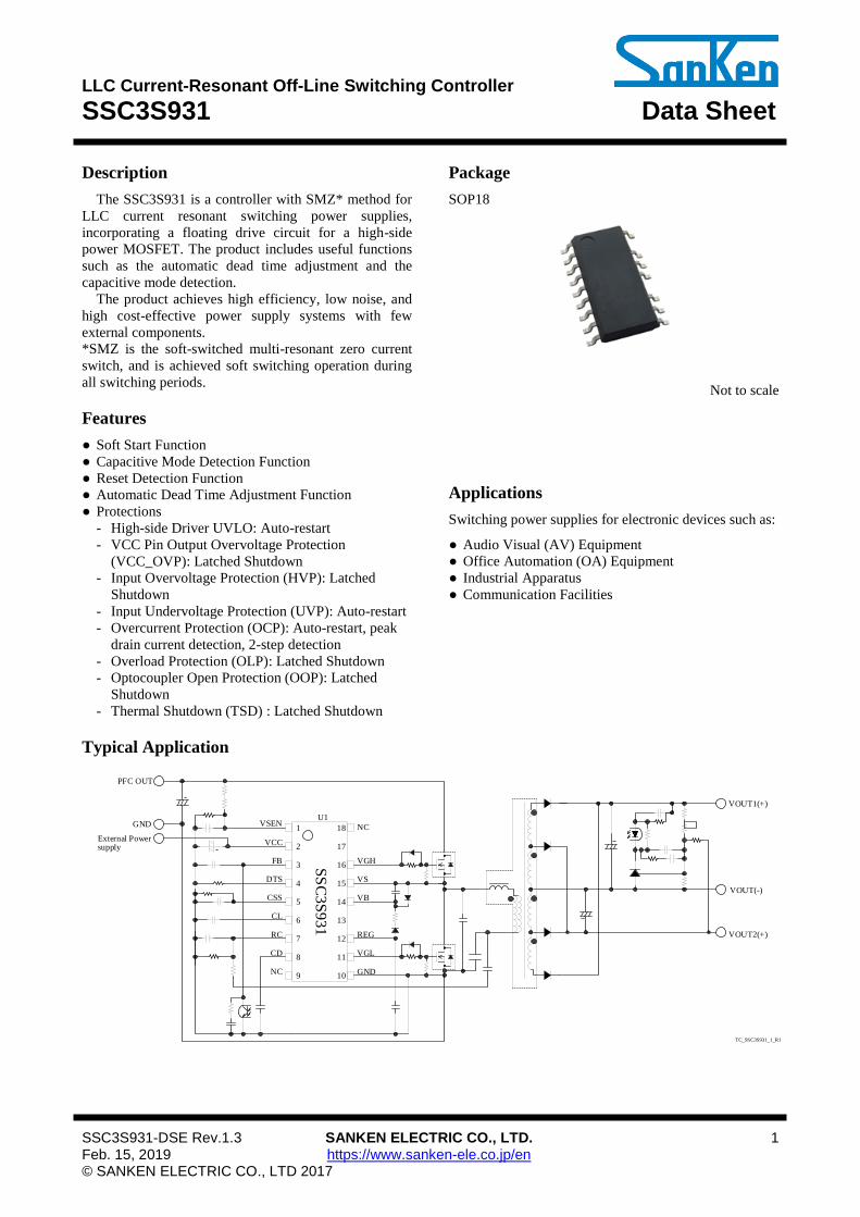
Typical Application
Package
SOP18
Not to scale
Applications
Switching power supplies for electronic devices such as:
● Audio Visual (AV) Equipment
● Office Automation (OA) Equipment
● Industrial Apparatus
● Communication Facilities
余白上 35mm
DTS
VSEN
VCC
FB
NC
VGH
VS
VB
REG
CSS
CL
CD VGL
GND
RC
NC
VOUT2(+)
VOUT(-)
VOUT1(+)
1
15
16
17
18
4
3
2
U1
SS
C3
S9
31
7
6
5
12
13
14
9
8
10
11
TC_SSC3S931_1_R1
PFC OUT
GND
External Power supply
SSC3S931
SSC3S931-DSE Rev.1.3 SANKEN ELECTRIC CO., LTD. 2 Feb. 15, 2019 https://www.sanken-ele.co.jp/en © SANKEN ELECTRIC CO., LTD 2017
Contents
Description ------------------------------------------------------------------------------------------------------ 1
Contents --------------------------------------------------------------------------------------------------------- 2
1. Absolute Maximum Ratings ----------------------------------------------------------------------------- 3
2. Electrical Characteristics -------------------------------------------------------------------------------- 4
3. Block Diagram --------------------------------------------------------------------------------------------- 6
4. Pin Configuration Definitions --------------------------------------------------------------------------- 7
5. Typical Application --------------------------------------------------------------------------------------- 7
6. Physical Dimensions -------------------------------------------------------------------------------------- 8
7. Marking Diagram ----------------------------------------------------------------------------------------- 8
8. Operational Description --------------------------------------------------------------------------------- 9 8.1 Resonant Circuit Operation ----------------------------------------------------------------------- 9 8.2 Startup Operation --------------------------------------------------------------------------------- 12 8.3 Soft Start Function -------------------------------------------------------------------------------- 12 8.4 Minimum and Maximum Switching Frequency Setting ----------------------------------- 13 8.5 High-side Driver ----------------------------------------------------------------------------------- 13 8.6 Constant Voltage Control Operation ---------------------------------------------------------- 13 8.7 Dead Time ------------------------------------------------------------------------------------------ 14
8.7.1 When Using Automatic Dead Time Adjustment Function -------------------------- 14 8.7.2 When Using Fixed Minimum Dead Time Value -------------------------------------- 14
8.8 Capacitive Mode Detection Function ---------------------------------------------------------- 15 8.9 Reset Detection Function ------------------------------------------------------------------------ 16 8.10 VCC Pin Overvoltage Protection (VCC_OVP) ---------------------------------------------- 17 8.11 Input Overvoltage Protection (HVP), Input Undervoltage Protection (UVP) --------- 17 8.12 Overcurrent Protection (OCP) ----------------------------------------------------------------- 17
8.12.1 Overcurrent Protection 1 (OCP1) -------------------------------------------------------- 18 8.12.2 Overcurrent Protection 2 (OCP2) -------------------------------------------------------- 18
8.13 Overload Protection (OLP) ---------------------------------------------------------------------- 18 8.14 Optocoupler Open Protection (OOP) --------------------------------------------------------- 18 8.15 Thermal Shutdown (TSD) ----------------------------------------------------------------------- 19
9. Design Notes ---------------------------------------------------------------------------------------------- 19 9.1 External Components ---------------------------------------------------------------------------- 19
9.1.1 Input and Output Electrolytic Capacitors ---------------------------------------------- 19 9.1.2 Resonant Transformer --------------------------------------------------------------------- 19 9.1.3 Current Detection Resistor, ROCP -------------------------------------------------------- 19 9.1.4 Current Resonant Capacitor, Ci --------------------------------------------------------- 19 9.1.5 Gate Pin Peripheral Circuit --------------------------------------------------------------- 19
9.2 PCB Trace Layout and Component Placement --------------------------------------------- 20
10. Pattern Layout Example ------------------------------------------------------------------------------- 22
Important Notes ---------------------------------------------------------------------------------------------- 23
SSC3S931
SSC3S931-DSE Rev.1.3 SANKEN ELECTRIC CO., LTD. 3 Feb. 15, 2019 https://www.sanken-ele.co.jp/en © SANKEN ELECTRIC CO., LTD 2017
1. Absolute Maximum Ratings
Current polarities are defined as follows: current going into the IC (sinking) is positive current (+); and current
coming out of the IC (sourcing) is negative current (−).
Unless otherwise specified, TA is 25°C.
Characteristic
Symbol Pins Rating Unit
VSEN Pin Sink Current ISEN 1 − 10 1.0 mA
Control Part Input Voltage VCC 2 − 10 −0.3 to 35 V
FB Pin Voltage VFB 3 − 10 −0.3 to 6 V
DTS Pin Voltage VDTS 4 − 10 −0.3 to VREG V
CSS Pin Voltage VCSS 5 − 10 −0.3 to 6 V
CL Pin Voltage VCL 6 − 10 −0.3 to 6 V
RC Pin Voltage VRC 7 − 10 −6 to 6 V
CD Pin Voltage VCD 8 − 10 −0.3 to 6 V
VGL Pin Voltage VGL 11 − 10 −0.3 to VREG + 0.3 V
REG Pin Source Current IREG 12 − 10 −10.0 mA
Voltage Between VB Pin and VS Pin VB−VS 14 − 15 −0.3 to 20.0 V
VS Pin Voltage VS 15 − 10 −1 to 600 V
VGH Pin Voltage VGH 16 − 10 VS − 0.3 to VB + 0.3 V
Operating Ambient Temperature TOP ― −40 to 85 °C
Storage Temperature Tstg ― −40 to 125 °C
Junction Temperature Tj ― 150 °C
* Surge voltage withstand (Human body model) of No.14, 15 and 16 is guaranteed 1000V. Other pins are guaranteed
2000 V.
SSC3S931
SSC3S931-DSE Rev.1.3 SANKEN ELECTRIC CO., LTD. 4 Feb. 15, 2019 https://www.sanken-ele.co.jp/en © SANKEN ELECTRIC CO., LTD 2017
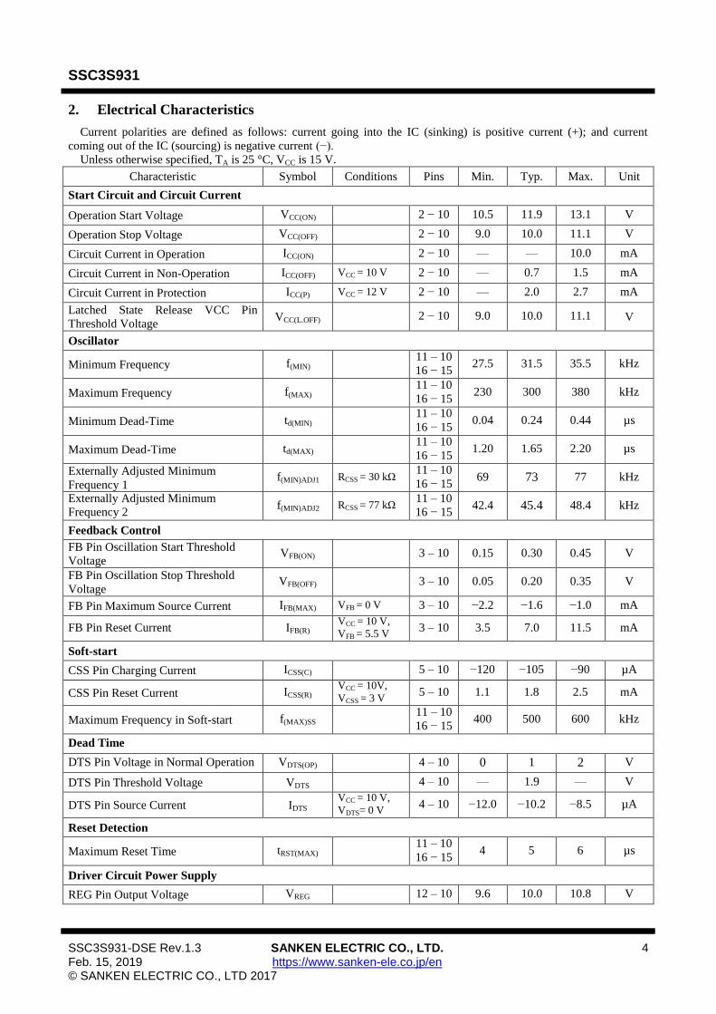
2. Electrical Characteristics
Current polarities are defined as follows: current going into the IC (sinking) is positive current (+); and current
coming out of the IC (sourcing) is negative current (−).
Unless otherwise specified, TA is 25 °C, VCC is 15 V.
Characteristic
Symbol Conditions Pins Min. Typ. Max. Unit
Start Circuit and Circuit Current
Operation Start Voltage VCC(ON) 2 − 10 10.5 11.9 13.1 V
Operation Stop Voltage VCC(OFF) 2 − 10 9.0 10.0 11.1 V
Circuit Current in Operation ICC(ON) 2 − 10 — — 10.0 mA
Circuit Current in Non-Operation ICC(OFF) VCC = 10 V 2 − 10 — 0.7 1.5 mA
Circuit Current in Protection ICC(P) VCC = 12 V 2 − 10 — 2.0 2.7 mA
Latched State Release VCC Pin
Threshold Voltage VCC(L.OFF) 2 − 10 9.0 10.0 11.1 V
Oscillator
Minimum Frequency f(MIN) 11 – 10
16 − 15 27.5 31.5 35.5 kHz
Maximum Frequency f(MAX) 11 – 10
16 − 15 230 300 380 kHz
Minimum Dead-Time td(MIN) 11 – 10
16 − 15 0.04 0.24 0.44 µs
Maximum Dead-Time td(MAX) 11 – 10
16 − 15 1.20 1.65 2.20 µs
Externally Adjusted Minimum
Frequency 1 f(MIN)ADJ1 RCSS = 30 kΩ
11 – 10
16 − 15 69 73 77 kHz
Externally Adjusted Minimum
Frequency 2 f(MIN)ADJ2 RCSS = 77 kΩ
11 – 10
16 − 15 42.4 45.4 48.4 kHz
Feedback Control
FB Pin Oscillation Start Threshold
Voltage VFB(ON) 3 – 10 0.15 0.30 0.45 V
FB Pin Oscillation Stop Threshold
Voltage VFB(OFF) 3 – 10 0.05 0.20 0.35 V
FB Pin Maximum Source Current IFB(MAX) VFB = 0 V 3 – 10 −2.2 −1.6 −1.0 mA
FB Pin Reset Current IFB(R) VCC = 10 V,
VFB = 5.5 V 3 – 10 3.5 7.0 11.5 mA
Soft-start
CSS Pin Charging Current ICSS(C) 5 – 10 −120 −105 −90 µA
CSS Pin Reset Current ICSS(R) VCC = 10V,
VCSS = 3 V 5 – 10 1.1 1.8 2.5 mA
Maximum Frequency in Soft-start f(MAX)SS 11 – 10
16 − 15 400 500 600 kHz
Dead Time
DTS Pin Voltage in Normal Operation VDTS(OP) 4 – 10 0 1 2 V
DTS Pin Threshold Voltage VDTS 4 – 10 — 1.9 — V
DTS Pin Source Current IDTS VCC = 10 V,
VDTS= 0 V 4 – 10 −12.0 −10.2 −8.5 µA
Reset Detection
Maximum Reset Time tRST(MAX) 11 – 10
16 − 15 4 5 6 µs
Driver Circuit Power Supply
REG Pin Output Voltage VREG 12 – 10 9.6 10.0 10.8 V
SSC3S931
SSC3S931-DSE Rev.1.3 SANKEN ELECTRIC CO., LTD. 5 Feb. 15, 2019 https://www.sanken-ele.co.jp/en © SANKEN ELECTRIC CO., LTD 2017
Characteristic
Symbol Conditions Pins Min. Typ. Max. Unit
High-side Driver
High-side Driver Operation Start
Voltage VBUV(ON) 14 – 15 5.7 6.8 7.9 V
High-side Driver Operation Stop
Voltage VBUV(OFF) 14 – 15 5.5 6.4 7.3 V
Driver Circuit
VGL,VGH Pin Source Current 1 IGL(SRC)1
IGH(SRC)1
VREG = 10.5 V,
VB = 10.5 V,
VGL = 0 V,
VGH = 0 V
11 – 10
16 − 15 — –540 — mA
VGL,VGH Pin Sink Current 1 IGL(SNK)1
IGH(SNK)1
VREG = 10.5 V,
VB = 10.5 V,
VGL = 10.5 V,
VGH = 10.5 V
11 – 10
16 − 15 — 1.50 — A
VGL,VGH Pin Source Current 2 IGL(SRC)2
IGH(SRC)2
VREG = 11.5 V,
VB = 11.5 V,
VGL = 10 V,
VGH = 10 V
11 – 10
16 − 15 −140 −90 −40 mA
VGL,VGH Pin Sink Current 2 IGL(SNK)2
IGH(SNK)2
VREG = 11.5 V,
VB = 11.5 V,
VGL = 1.5 V,
VGH = 1.5 V
11 – 10
16 − 15 140 230 360 mA
VCC Pin Overvoltage Protection (VCC_OVP)
VCC Pin OVP Threshold Voltage VCC(OVP) 2 – 10 30.0 32.0 34.0 V
Current Resonant and Overcurrent Protection(OCP)
Capacitive Mode Detection Voltage 1 VRC1 7 – 10 0.02 0.10 0.18 V
−0.18 −0.10 −0.02 V
Capacitive Mode Detection Voltage 2 VRC2 7 – 10 0.20 0.30 0.40 V
−0.40 −0.30 −0.20 V
RC Pin Threshold Voltage (Low) VRC(L) 7 – 10 1.80 1.90 2.00 V
−2.00 −1.90 −1.80 V
RC Pin Threshold Voltage (High) VRC(H) 7 – 10 2.62 2.80 2.98 V
−2.98 −2.80 −2.62 V
CSS Pin Sink Current (Low) ICSS(L) VCSS = 3 V 5 – 10 1.1 1.8 2.5 mA
CSS Pin Sink Current (High) ICSS(H) VCSS = 3 V 5 – 10 13.0 20.5 28.0 mA
Overload Protection (OLP)
CL pin OLP Threshold Voltage VCL(OLP) 6 – 10 3.9 4.2 4.5 V
CL Pin Source Current 1 ICL(SRC)1 VCL = 0.5 V 6 – 10 −29 −17 −5 μA
CL Pin Source Current 2 ICL(SRC)2 VCL = 3 V 6 – 10 −180 −135 −90 μA
CL Pin Sink Current ICL(SNK) VCL = 3 V 6 – 10 10 30 50 μA
Input Overvoltage Protection (HVP), Input Undervoltage Protection (UVP)
VSEN Pin UVP Release Threshold
Voltage VSEN(ON) 1 – 10 1.248 1.300 1.352 V
VSEN Pin UVP Threshold Voltage VSEN(OFF) 1 – 10 1.056 1.100 1.144 V
VSEN Pin HVP Threshold Voltage VSEN(HVP)
1 – 10 5.3 5.6 5.9 V
VSEN Pin Clamp Voltage VSEN (CLAMP) 1 – 10 10.0 — — V
SSC3S931
SSC3S931-DSE Rev.1.3 SANKEN ELECTRIC CO., LTD. 6 Feb. 15, 2019 https://www.sanken-ele.co.jp/en © SANKEN ELECTRIC CO., LTD 2017
Characteristic
Symbol Conditions Pins Min. Typ. Max. Unit
Optocoupler Open Protection (OOP)
FB Pin Open Detection Threshold
Voltage VFB(OOP) 3 – 10 4.2 4.6 5.0 V
CD Pin Threshold Voltage VCD 8 – 10 2.8 3.0 3.2 V CD Pin Source Current ICD(SRC) VCD = 0 V 8 – 10 –29 –20 –11 μA CD Pin Sink Current ICD(SNK) VCD = 2.5 V 8 – 10 28 43 58 μA
CD Pin Reset Current ICD(R) VCD = 2 V 8 – 10 1.0 2.5 4.0 mA Thermal Shutdown (TSD)
Thermal Shutdown Temperature Tj(TSD) — 140 — — °C
Thermal Resistance
Junction to Ambient Thermal
Resistance θj-A — — — 95 °C/W
3. Block Diagram
Start/Stop/Reg./Bias/
OVP
MainInput Sense
FB Control Freq. Control
Dead Time
UVLO
Level Shift
OC Detector
RV Detector
RC Detector
Freq. ( max.)
Soft Start/OC/Freq. (min.)/Adj.
VCCGND
2
10
1
3
5
14
16
15
7
6
8
4
11
12
VCC
GND
VSEN
FB
CSS
VB
VGH
VS
REG
VGL
RC
CL
CD
DTS
High Side Driver
BD_SSC3S931_R1
FB Detector
OLP
SSC3S931
SSC3S931-DSE Rev.1.3 SANKEN ELECTRIC CO., LTD. 7 Feb. 15, 2019 https://www.sanken-ele.co.jp/en © SANKEN ELECTRIC CO., LTD 2017
4. Pin Configuration Definitions
1
2
3
4
5
6
7
8
9
18
16
15
14
12
11
10
VCC
FB
DTS
CSS
CL
RC
CD
NC
NC
VGH
VS
VB
REG
VGL
GND
VSEN
Number Name Description 1 VSEN Mains input voltage detection signal input
2 VCC Supply voltage input for the IC with VCC pin
overvoltage protection (VCC_OVP)
3 FB Feedback signal input for constant voltage control
and optocoupler open protection (OOP) signal input
4 DTS Dead time control selection: a fixed on the minimum
value, or an automatically adjustment
5 CSS Soft-start setting capacitor connection 6 CL Overload detection (OLP) capacitor connection
7 RC Resonant current detection signal input and
overcurrent protection (OCP) signal input
8 CD Delay time setting capacitor connection for
optocoupler open protection (OOP)
9 NC Not connected
10 GND Ground 11 VGL Low-side gate drive output 12 REG Supply voltage output for gate drive circuit 13 — Pin removed 14 VB Supply voltage input for high-side driver with UVLO 15 VS Floating ground for high-side driver 16 VGH High-side gate drive output 17 — Pin removed 18 NC Not connected
5. Typical Application
DTS
VSEN
VCC
FB
NC
VGH
VS
VB
REG
CSS
CL
CD VGL
GND
RC
NC
VOUT2(+)
VOUT(-)
VOUT1(+)
1
15
16
17
18
4
3
2
U1
SS
C3
S931
7
6
5
12
13
14
9
8
10
11
TC_SSC3S931_2_R1
PFC OUT
GND
External Power supply
C1
R1
R2R3
R4
R5
R7
R6
R8
R9
R10
R11
R12
R13
R51
R52
R53
R54
R55
R56
R57
C2
C3
C4
C5
C6C7
C8
C10 C11
C9
CV
Ci
C12
C51
C52
C53
C54
C55
D51
D52
D54
D53
PC1
U51
PC1
D2
D4
D3
Q(H)
Q(L)
T1
D1
Figure 5-1. Typical Application
SSC3S931
SSC3S931-DSE Rev.1.3 SANKEN ELECTRIC CO., LTD. 8 Feb. 15, 2019 https://www.sanken-ele.co.jp/en © SANKEN ELECTRIC CO., LTD 2017
6. Physical Dimensions
● SOP18
7. Marking Diagram
1
18
Part NumberS S C 3 S 9 3 1
X X X X
Control Number
Lot Number:
Y is the last digit of the year of manufacture (0 to 9)
M is the month of the year (1 to 9, O, N, or D)
D is a period of days:
1: the first 10 days of the month (1st to 10th)
2: the second 10 days of the month (11th to 20th)
3: the last 10–11 days of the month (21st to 31st)
S K Y M D
NOTES:
- Dimensions in millimeters
- Pb-free
SSC3S931
SSC3S931-DSE Rev.1.3 SANKEN ELECTRIC CO., LTD. 9 Feb. 15, 2019 https://www.sanken-ele.co.jp/en © SANKEN ELECTRIC CO., LTD 2017
8. Operational Description
All of the parameter values used in these descriptions
are typical values, unless they are specified as minimum
or maximum. Current polarities are defined as follows:
current going into the IC (sinking) is positive current
(+); and current coming out of the IC (sourcing) is
negative current (−). Q(H) and Q(L) indicate a high-side
power MOSFET and a low-side power MOSFET
respectively. Ci and CV indicate a current resonant
capacitor and a voltage resonant capacitor, respectively.
8.1 Resonant Circuit Operation
Figure 8-1 shows a basic RLC series resonant circuit.
The impedance of the circuit, Ż, is as the following
Equation.
(1)
where ω is angular frequency; and ω = 2πf.
Thus,
(2)
When the frequency, f, changes, the impedance of
resonant circuit will change as shown in Figure 8-2.
R L C
Figure 8-1. RLC Series Resonant Circuit
f0 Frequency
Inductance areaCapacitance area
Imp
edan
ce
R
Figure 8-2. Impedance of Resonant Circuit
When 2πfL = 1/2πfC, Ż of Equation (2) becomes the
minimum value, R (see Figure 8-2). In the case, ω is
calculated by Equation (3).
(3)
The frequency in which Ż becomes minimum value is
called a resonant frequency, f0. The higher frequency
area than is an inductance area. The lower frequency
area than is a capacitance area.
From Equation (3), is as follows:
(4)
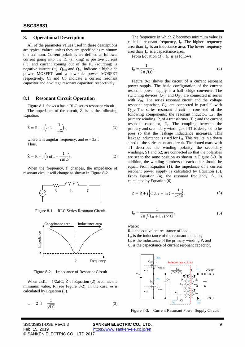
Figure 8-3 shows the circuit of a current resonant
power supply. The basic configuration of the current
resonant power supply is a half-bridge converter. The
switching devices, Q(H) and Q(L), are connected in series
with VIN. The series resonant circuit and the voltage
resonant capacitor, CV, are connected in parallel with
Q(L). The series resonant circuit is consisted of the
following components: the resonant inductor, LR; the
primary winding, P, of a transformer, T1; and the current
resonant capacitor, Ci. The coupling between the
primary and secondary windings of T1 is designed to be
poor so that the leakage inductance increases. This
leakage inductance is used for LR. This results in a down
sized of the series resonant circuit. The dotted mark with
T1 describes the winding polarity, the secondary
windings, S1 and S2, are connected so that the polarities
are set to the same position as shown in Figure 8-3. In
addition, the winding numbers of each other should be
equal. From Equation (1), the impedance of a current
resonant power supply is calculated by Equation (5).
From Equation (4), the resonant frequency, , is
calculated by Equation (6).
(5)
(6)
where:
R is the equivalent resistance of load,
LR is the inductance of the resonant inductor,
LP is the inductance of the primary winding P, and
Ci is the capacitance of current resonant capacitor.
Cv
Ci
LR
Q(H)
P
Series resonant circuit
T1
S1
S2
VOUT
(+)
(−)
VIN
VGH
VGL
Q(L)
VDS(L)
VDS(H)
VCi
ID(H)
ID(L)
ICi IS2
IS1
LP
Figure 8-3. Current Resonant Power Supply Circuit
SSC3S931
SSC3S931-DSE Rev.1.3 SANKEN ELECTRIC CO., LTD. 10 Feb. 15, 2019 https://www.sanken-ele.co.jp/en © SANKEN ELECTRIC CO., LTD 2017
In the current resonant power supply, Q(H) and Q(L) are
alternatively turned on and off. The on and off times of
them are equal. There is a dead time between the on
periods of Q(H) and Q(L). During the dead time, Q(H) and
Q(L) are in off status.
In the current resonant power supply, the frequency is
controlled. When the output voltage decreases, the IC
decreases the switching frequency so that the output
power is increased to keep a constant output voltage.
This must be controlled in the inductance area ( ). Since the winding current is delayed from the
winding voltage in the inductance area, the turn-on
operates in a ZCS (Zero Current Switching); and the
turn-off operates in a ZVS (Zero Voltage Switching).
Thus, the switching losses of Q(H) and Q(L) are nearly
zero. In the capacitance area ( ), the current
resonant power supply operates as follows: When the
output voltage decreases, the switching frequency is
decreased; and then, the output power is more decreased.
Therefore, the output voltage cannot be kept constant.
Since the winding current goes ahead of the winding
voltage in the capacitance area, Q(H) and Q(L) operate in
the hard switching. This results in the increases of a
power loss. This operation in the capacitance area is
called the capacitive mode operation. The current
resonant power supply must be operated without the
capacitive mode operation (for more details, see Section
8.8).
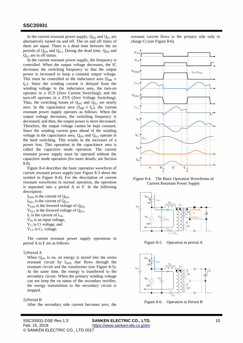
Figure 8-4 describes the basic operation waveform of
current resonant power supply (see Figure 8-3 about the
symbol in Figure 8-4). For the description of current
resonant waveforms in normal operation, the operation
is separated into a period A to F. In the following
description:
ID(H) is the current of Q(H),
ID(L) is the current of Q(L),
VF(H) is the forwerd voltage of Q(H),
VF(L) is the forwerd voltage of Q(L),
IL is the current of LR,
VIN is an input voltage,
VCi is Ci voltage, and
VCV is CV voltage.
The current resonant power supply operations in
period A to F are as follows:
1) Period A
When Q(H) is on, an energy is stored into the series
resonant circuit by ID(H) that flows through the
resonant circuit and the transformer (see Figure 8-5).
At the same time, the energy is transferred to the
secondary circuit. When the primary winding voltage
can not keep the on status of the secondary rectifier,
the energy transmittion to the secondary circuit is
stopped.
2) Period B
After the secondary side current becomes zero, the
resonant current flows to the primary side only to
charge Ci (see Figure 8-6).
ID(L)
ID(H)
IS1
VGL
VGH
VDS(L)
ICi
VCi
IS2
A B
C
D E
F
VIN+VF(H)VDS(H)
VIN
Figure 8-4. The Basic Operation Waveforms of
Current Resonant Power Supply
Cv
Ci
LR
Q(H)
Q(L)
LP
ON
OFF
ID(H)
VIN
S1
S2
IS1
VCV
VCi
Figure 8-5. Operation in period A
Cv
Ci
LR
Q(H)
Q(L)
LP
ON
OFF
ID(H)
VIN
S1
S2
Figure 8-6. Operation in Period B
SSC3S931
SSC3S931-DSE Rev.1.3 SANKEN ELECTRIC CO., LTD. 11 Feb. 15, 2019 https://www.sanken-ele.co.jp/en © SANKEN ELECTRIC CO., LTD 2017
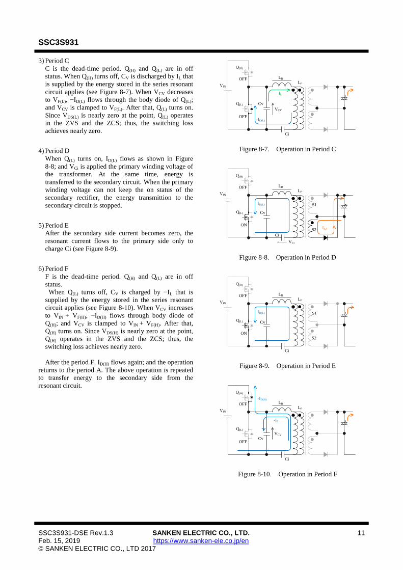
3) Period C
C is the dead-time period. Q(H) and Q(L) are in off
status. When Q(H) turns off, CV is discharged by IL that
is supplied by the energy stored in the series resonant
circuit applies (see Figure 8-7). When VCV decreases
to VF(L), −ID(L) flows through the body diode of Q(L);
and VCV is clamped to VF(L). After that, Q(L) turns on.
Since VDS(L) is nearly zero at the point, Q(L) operates
in the ZVS and the ZCS; thus, the switching loss
achieves nearly zero.
4) Period D
When Q(L) turns on, ID(L) flows as shown in Figure
8-8; and VCi is applied the primary winding voltage of
the transformer. At the same time, energy is
transferred to the secondary circuit. When the primary
winding voltage can not keep the on status of the
secondary rectifier, the energy transmittion to the
secondary circuit is stopped.
5) Period E
After the secondary side current becomes zero, the
resonant current flows to the primary side only to
charge Ci (see Figure 8-9).
6) Period F
F is the dead-time period. Q(H) and Q(L) are in off
status.
When Q(L) turns off, CV is charged by −IL that is
supplied by the energy stored in the series resonant
circuit applies (see Figure 8-10). When VCV increases
to VIN + VF(H), −ID(H) flows through body diode of
Q(H); and VCV is clamped to VIN + VF(H). After that,
Q(H) turns on. Since VDS(H) is nearly zero at the point,
Q(H) operates in the ZVS and the ZCS; thus, the
switching loss achieves nearly zero.
After the period F, ID(H) flows again; and the operation
returns to the period A. The above operation is repeated
to transfer energy to the secondary side from the
resonant circuit.
Cv
Ci
LR
Q(H)
Q(L)
LP
OFF
OFF
IL
VIN
-ID(L)
VCV
Figure 8-7. Operation in Period C
Cv
Ci
LR
Q(H)
Q(L)
LP
OFF
ON
VIN
ID(L)
IS2
S1
S2
VCi
Figure 8-8. Operation in Period D
Cv
Ci
LR
Q(H)
Q(L)
LP
OFF
ON
VIN
ID(L) S1
S2
Figure 8-9. Operation in Period E
Cv
Ci
LR
Q(H)
Q(L)
LP
OFF
OFF
-IL
VIN
-ID(H)
VCV
Figure 8-10. Operation in Period F
SSC3S931
SSC3S931-DSE Rev.1.3 SANKEN ELECTRIC CO., LTD. 12 Feb. 15, 2019 https://www.sanken-ele.co.jp/en © SANKEN ELECTRIC CO., LTD 2017
8.2 Startup Operation
Figure 8-11 and Figure 8-12 show the VCC pin
peripheral circuit and the startup waveforms,
respectively. The VCC pin is a power supply input pin
for a control circuit and is supplied from an external
power supply. When the VCC pin voltage increases to
the Operation Start Voltage, VCC(ON) = 11.9 V, the
control circuit starts operation. When the VCC pin
voltage decreases to the Operation Stop Voltage,
VCC(OFF) = 10.0 V, the control circuit is stopped by the
undervoltage lockout (UVLO) circuit, and returns to the
state before startup (see Figure 8-13).
When the IC satisfies all following conditions, the IC
starts a switching operation:
● VCC pin voltage ≥ VCC(ON) = 11.9 V
● VSEN pin voltage ≥ VSEN(ON) = 1.300 V
● FB pin voltage ≥ VFB(ON)= 0.30 V
5 4
2
CSS
VCC
GND
U1
VSEN
C2
R1
R2
R3C3
C6
External Power Supply
C11
R6
Figure 8-11. VCC Pin Peripheral Circuit
VCC Pin Voltage
VSEN Pin Voltage
FB Pin Voltage
VGL Pin Voltage
VCC(ON)
VSEN(ON)
VFB(ON)
Time
REG Pin Voltage VREG
0
0
0
0
Figure 8-12. Startup Waveforms
ICC
VCC(OFF) VCC(ON)VCC Pin Voltage
StartStop
Figure 8-13. VCC vs. ICC
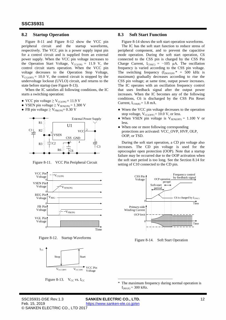
8.3 Soft Start Function
Figure 8-14 shows the soft start operation waveforms.
The IC has the soft start function to reduce stress of
peripheral component, and to prevent the capacitive
mode operation. During the soft start operation, C6
connected to the CSS pin is charged by the CSS Pin
Charge Current, ICSS(C) = −105 μA. The oscillation
frequency is varied according to the CSS pin voltage.
The switching frequency (f(MAX)SS * = 500 kHz is
maximum) gradually decreases according to rise the
CSS pin voltage; at same time, output power increases.
The IC operates with an oscillation frequency control
that uses feedback signal after the output power
increases. When the IC becomes any of the following
conditions, C6 is discharged by the CSS Pin Reset
Current, ICSS(R) = 1.8 mA.
● Wnen the VCC pin voltage decreases to the operation
stop voltage, VCC(OFF) = 10.0 V, or less.
● When VSEN pin voltage is VSEN(OFF) = 1.100 V or
less.
● When one or more following corresponding
protections are activated: VCC_OVP, HVP, OLP,
OOP, or TSD.
During the soft start operation, a CD pin voltage also
increases. The CD pin voltage is used for the
optocoupler open protection (OOP). Note that a startup
failure may be occurred due to the OOP activation when
the soft start period is too long. See the Section 8.14 for
setting of C10 connected to the CD pin.
CSS Pin Voltage
Primary-side Winding Current
0
0
OCP limit
C6 is charged by ICSS(C)
Time
Time
Soft-start period
OCP operation peropd
Frequency control by feedback signal
Figure 8-14. Soft Start Operation
* The maximum frequency during normal operation is
f(MAX) = 300 kHz.
SSC3S931
SSC3S931-DSE Rev.1.3 SANKEN ELECTRIC CO., LTD. 13 Feb. 15, 2019 https://www.sanken-ele.co.jp/en © SANKEN ELECTRIC CO., LTD 2017
8.4 Minimum and Maximum Switching
Frequency Setting
The minimum switching frequency is determined by
the resistance of R6 connected to the CSS pin. Figure
8-15 shows the relationship of R6 and f(MIN)ADJ that is the
external adjustment minimum frequency.
The f(MIN)ADJ must be set more than the resonant
frequency, f0, under the condition of the minimum mains
input voltage and the maximum output power. The
maximum switching frequency, fMAX, is determined by
the inductance and the capacitance of a resonant circuit.
The fMAX must be set less than the maximum frequency,
f(MAX) = 300 kHz.
Figure 8-15. R6 vs. f(MIN)ADJ
8.5 High-side Driver
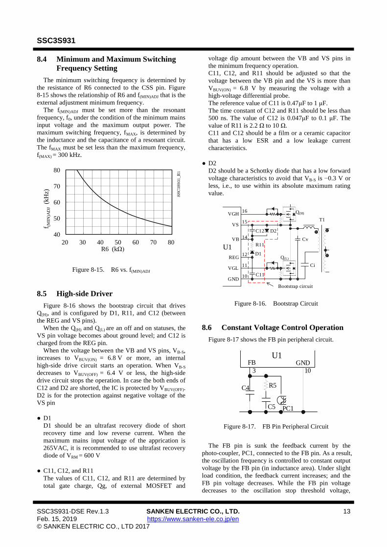
Figure 8-16 shows the bootstrap circuit that drives
Q(H), and is configured by D1, R11, and C12 (between
the REG and VS pins).
When the Q(H) and Q(L) are an off and on statuses, the
VS pin voltage becomes about ground level; and C12 is
charged from the REG pin.
When the voltage between the VB and VS pins, VB-S,
increases to VBUV(ON) = 6.8 V or more, an internal
high-side drive circuit starts an operation. When VB-S
decreases to VBUV(OFF) = 6.4 V or less, the high-side
drive circuit stops the operation. In case the both ends of
C12 and D2 are shorted, the IC is protected by VBUV(OFF).
D2 is for the protection against negative voltage of the
VS pin
● D1
D1 should be an ultrafast recovery diode of short
recovery time and low reverse current. When the
maximum mains input voltage of the apprication is
265VAC, it is recommended to use ultrafast recovery
diode of VRM = 600 V
● C11, C12, and R11
The values of C11, C12, and R11 are determined by
total gate charge, Qg, of external MOSFET and
voltage dip amount between the VB and VS pins in
the minimum frequency operation.
C11, C12, and R11 should be adjusted so that the
voltage between the VB pin and the VS is more than
VBUV(ON) = 6.8 V by measuring the voltage with a
high-voltage differential probe.
The reference value of C11 is 0.47μF to 1 μF.
The time constant of C12 and R11 should be less than
500 ns. The value of C12 is 0.047μF to 0.1 μF. The
value of R11 is 2.2 Ω to 10 Ω.
C11 and C12 should be a film or a ceramic capacitor
that has a low ESR and a low leakage current
characteristics.
● D2
D2 should be a Schottky diode that has a low forward
voltage characteristics to avoid that VB-S is −0.3 V or
less, i.e., to use within its absolute maximum rating
value.
VGH
VS
VB
REG
VGL
GND
T115
16
U112
14
10
11
R11
D1
C11
C12 D2
Bootstrap circuit
Q(H)
Q(L)
Cv
Ci
Figure 8-16. Bootstrap Circuit
8.6 Constant Voltage Control Operation
Figure 8-17 shows the FB pin peripheral circuit.
3 10
FB GNDU1
C4
PC1C5
R5
Figure 8-17. FB Pin Peripheral Circuit
The FB pin is sunk the feedback current by the
photo-coupler, PC1, connected to the FB pin. As a result,
the oscillation frequency is controlled to constant output
voltage by the FB pin (in inductance area). Under slight
load condition, the feedback current increases; and the
FB pin voltage decreases. While the FB pin voltage
decreases to the oscillation stop threshold voltage,
40
50
60
70
80
20 30 40 50 60 70 80
f (M
IN)A
DJ (
kH
z)
R6 (kΩ)
SS
C3S
93
1_R
1
SSC3S931
SSC3S931-DSE Rev.1.3 SANKEN ELECTRIC CO., LTD. 14 Feb. 15, 2019 https://www.sanken-ele.co.jp/en © SANKEN ELECTRIC CO., LTD 2017
VFB(OFF) = 0.20 V, or less, the IC stops switching
operation. This operation reduces switching loss, and
prevents the increasing of the secondary output voltage.
R5 and C5 are for a phase compensation adjustment.
C4 is for a high frequency noise rejection. The
secondary-side circuit should be designed so that the
collector current of PC1 is >1.6 mA that is the absolute
value of the maximum source current, IFB(MAX).
Especially, the current transfer ratio, CTR, of the photo
coupler should be taken an aging degradation into
account.
8.7 Dead Time
The dead time is the period when both the high-side
and the low-side power MOSFETs are off. If the dead
time is shorter than a voltage resonant period (see Figure
8-18), the power MOSFETs turns on/off during the
voltage resonant operation. In the case, the switching
loss increases due to hard switching operation of the
power MOSFETs.
The dead time is generated in the IC. The IC provides
the following two dead time controls selected by the
value of a resistor connected to the DTS pin:
automatically adjustment, or fixed minimum value.
Q(L) D-S Voltage, VDS(L)
VGL
VGH
Voltage resonant period
Loss increase by hard
switching operation
Dead time
Figure 8-18. ZVS Failure Operation Waveform
8.7.1 When Using Automatic Dead Time
Adjustment Function
When using the automatic dead time adjustment
function, set the startup sequence as follows: Set the
DTS pin voltage less than VDTS = 1.9 V, and then apply
VCC(ON) = 11.9 V or more to the VCC pin.
To set the DTS pin voltage less than 1.9 V connect a
resistor between the DTS and GND pins. The resistance
is about 100 kΩ with the effect of the DTS pin source
current (IDTS = −10.2 µA) taken into account.
This automatic dead time adjustment function
operates so that the IC detects a voltage resonant period
to automatically control the ZVS (Zero Voltage
Switching) operation of Q(H) and Q(L). This function
achieves the power supply application without a dead
time adjustment for each power supply specification, if
the voltage resonant period is varied according to the
power supply specifications such as an input voltage and
an output power. The VS pin detects the dv/dt periods
on the rising and falling voltage waveforms between
drain and source of the low-side power MOSFET (see
Figure 8-19). The dead time is determined by the
detected dv/dt period. As a result, the high-side and the
low-side power MOSFETs are automatically controlled
in the Zero Voltage Switching (ZVS) operation. This
function operates in the period from td(MIN) = 0.24 µs to
td(MAX) = 1.65 µs. Check that the Zero Current Switching
(ZCS) operation period is about 600 ns (i.e., the period
that the drain current flows through the body diode as
shown in Figure 8-20) based on actual operation in the
following conditions:
- When an output power is minimum in a maximum
input voltage specification.
- When an output power is maximum in a minimum
input voltage specification.
T1
Cv
Ci
VS
VGL
VGH
GND
U1
15
11
10
16
Main
RV DETECTOR
Low-side VDS(L)
Dead Time Period
dv
dt dt
On OnOff
VDS(L)
Figure 8-19. VS Pin and Dead Time Period
Q(H) Drain Current, ID(H)
Body diode flowing period: about 600 ns
Figure 8-20. ZCS Check Point
8.7.2 When Using Fixed Minimum Dead
Time Value
When using the fixed minimum dead time, set the
startup sequence as follows: Apply VDTS of 1.9 V or
more to the DTS pin, and then add VCC(ON) = 11.9 V or
more to the VCC pin.
Since the source current, IDTS = −10.2 µA, flows
through the DTS pin, the voltage is applied to DTS pin
by the resistor connected between the DTS and GND
pins. The resister should be set that the DTS pin voltage
is 1.9 V or more.
SSC3S931
SSC3S931-DSE Rev.1.3 SANKEN ELECTRIC CO., LTD. 15 Feb. 15, 2019 https://www.sanken-ele.co.jp/en © SANKEN ELECTRIC CO., LTD 2017
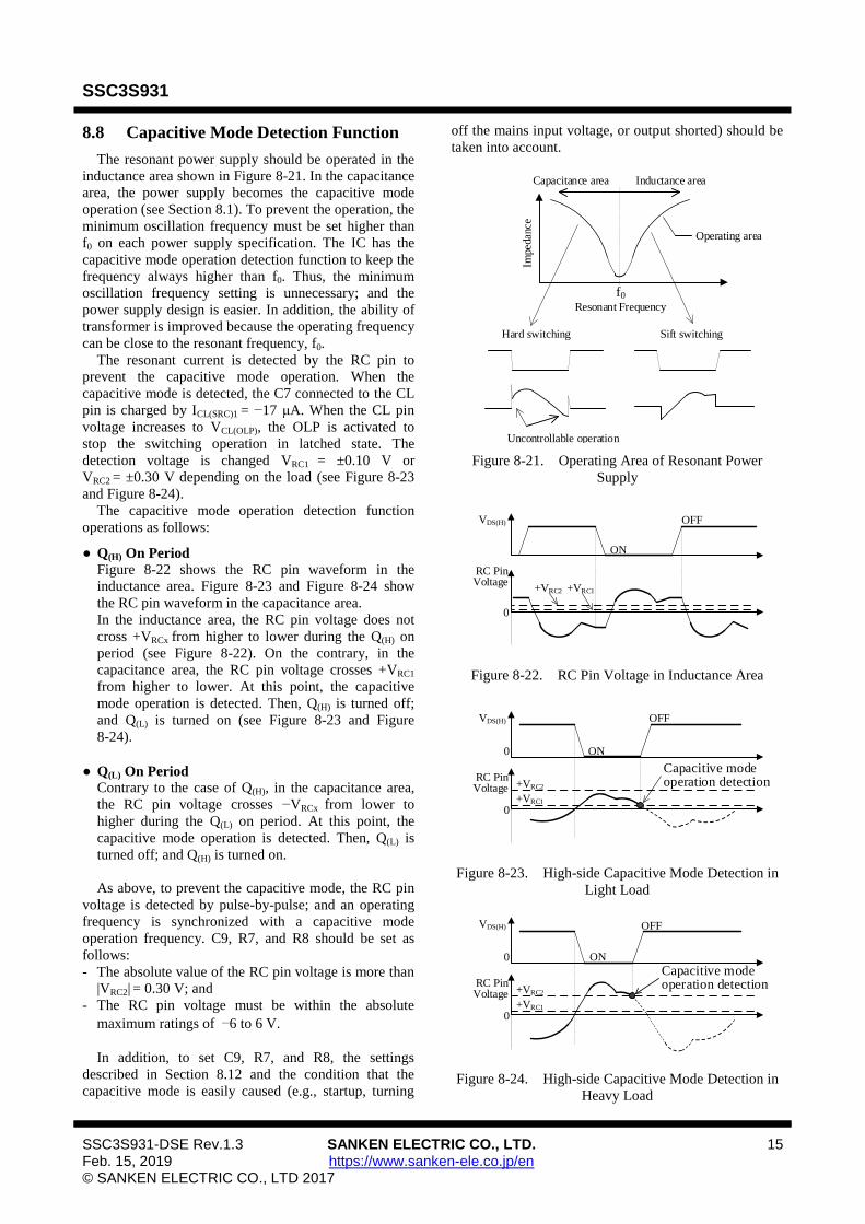
8.8 Capacitive Mode Detection Function
The resonant power supply should be operated in the
inductance area shown in Figure 8-21. In the capacitance
area, the power supply becomes the capacitive mode
operation (see Section 8.1). To prevent the operation, the
minimum oscillation frequency must be set higher than
f0 on each power supply specification. The IC has the
capacitive mode operation detection function to keep the
frequency always higher than f0. Thus, the minimum
oscillation frequency setting is unnecessary; and the
power supply design is easier. In addition, the ability of
transformer is improved because the operating frequency
can be close to the resonant frequency, f0.
The resonant current is detected by the RC pin to
prevent the capacitive mode operation. When the
capacitive mode is detected, the C7 connected to the CL
pin is charged by ICL(SRC)1 = −17 μA. When the CL pin
voltage increases to VCL(OLP), the OLP is activated to
stop the switching operation in latched state. The
detection voltage is changed VRC1 = ±0.10 V or
VRC2 = ±0.30 V depending on the load (see Figure 8-23
and Figure 8-24).
The capacitive mode operation detection function
operations as follows:
● Q(H) On Period
Figure 8-22 shows the RC pin waveform in the
inductance area. Figure 8-23 and Figure 8-24 show
the RC pin waveform in the capacitance area.
In the inductance area, the RC pin voltage does not
cross +VRCx from higher to lower during the Q(H) on
period (see Figure 8-22). On the contrary, in the
capacitance area, the RC pin voltage crosses +VRC1
from higher to lower. At this point, the capacitive
mode operation is detected. Then, Q(H) is turned off;
and Q(L) is turned on (see Figure 8-23 and Figure
8-24).
● Q(L) On Period Contrary to the case of Q(H), in the capacitance area,
the RC pin voltage crosses −VRCx from lower to
higher during the Q(L) on period. At this point, the
capacitive mode operation is detected. Then, Q(L) is
turned off; and Q(H) is turned on.
As above, to prevent the capacitive mode, the RC pin
voltage is detected by pulse-by-pulse; and an operating
frequency is synchronized with a capacitive mode
operation frequency. C9, R7, and R8 should be set as
follows:
- The absolute value of the RC pin voltage is more than
|VRC2| = 0.30 V; and
- The RC pin voltage must be within the absolute
maximum ratings of −6 to 6 V.
In addition, to set C9, R7, and R8, the settings
described in Section 8.12 and the condition that the
capacitive mode is easily caused (e.g., startup, turning
off the mains input voltage, or output shorted) should be
taken into account.
f0
Capacitance area Inductance area
Operating area
Impe
danc
e
Resonant Frequency
Hard switching Sift switching
Uncontrollable operation
Figure 8-21. Operating Area of Resonant Power
Supply
0
+VRC2
VDS(H)
ON
OFF
RC Pin Voltage
+VRC1
Figure 8-22. RC Pin Voltage in Inductance Area
VDS(H)
0
0
Capacitive mode operation detection
ON
OFF
+VRC2
RC Pin Voltage
+VRC1
Figure 8-23. High-side Capacitive Mode Detection in
Light Load
VDS(H)
0
0
Capacitive mode operation detection
ON
OFF
+VRC2
RC Pin Voltage
+VRC1
Figure 8-24. High-side Capacitive Mode Detection in
Heavy Load
SSC3S931
SSC3S931-DSE Rev.1.3 SANKEN ELECTRIC CO., LTD. 16 Feb. 15, 2019 https://www.sanken-ele.co.jp/en © SANKEN ELECTRIC CO., LTD 2017
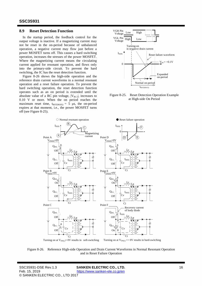
8.9 Reset Detection Function
In the startup period, the feedback control for the
output voltage is inactive. If a magnetizing current may
not be reset in the on-period because of unbalanced
operation, a negative current may flow just before a
power MOSFET turns off. This causes a hard switching
operation, increases the stresses of the power MOSFET.
Where the magnetizing current means the circulating
current applied for resonant operation, and flows only
into the primary-side circuit. To prevent the hard
switching, the IC has the reset detection function.
Figure 8-26 shows the high-side operation and the
reference drain current waveforms in a normal resonant
operation and a reset failure operation. To prevent the
hard switching operation, the reset detection function
operates such as an on period is extended until the
absolute value of a RC pin voltage, |VRC1|, increases to
0.10 V or more. When the on period reaches the
maximum reset time, tRST(MAX) = 5 μs, the on-period
expires at that moment, i.e., the power MOSFET turns
off (see Figure 8-25).
0VRC= +0.1V
Expandedon-period
ID(H)
VGL PinVoltage
LowHigh
Normal on-period
tRST(MAX)
Reset failure waveform
VGH PinVoltage
Turning-onin negative drain current
Low High
Figure 8-25. Reset Detection Operation Example
at High-side On Period
ID(H)
Cv
Ci
Lr
Q(H)
Q(L)
Lp
Cv
Ci
LrLp
Cv
Ci
LrLp
Cv
Ci
LrLp
Cv
Ci
LrLp
Cv
Ci
LrLp
A
B
C
E
F
0Magnetizing current
VDS(H)=0V
VDS(H)=0V
Turning on at VDS(L)= 0V results in soft-switching
VDS(H)=0V
VDS(H)=0V
Turning on at VDS(L) >> 0V results in hard-switching
Recovery current of body diode
Point A
Point B
Point C
Point D
Point E
Point F
Off
Off
On
Off
Off
Off
Off
Off
On
Off
Off
On
D
ID(H)
Q(H)
Q(L)
Q(H)
Q(L)
Q(H)
Q(L)
Q(H)
Q(L)
Q(H)
Q(L)
ID(H)
ID(H)
ID(H)
ID(H)
ID(H)
○ Normal resonant operation ● Reset failure operation
Figure 8-26. Reference High-side Operation and Drain Current Waveforms in Normal Resonant Operation
and in Reset Failure Operation
SSC3S931
SSC3S931-DSE Rev.1.3 SANKEN ELECTRIC CO., LTD. 17 Feb. 15, 2019 https://www.sanken-ele.co.jp/en © SANKEN ELECTRIC CO., LTD 2017
8.10 VCC Pin Overvoltage Protection
(VCC_OVP)
When the voltage between the VCC and GND pins is
applied to the VCC Pin OVP Threshold Voltage,
VCC(OVP) = 32.0 V, or more, the VCC pin overvoltage
protection (VCC_OVP) is activated; and the IC stops
switching operation in a latched state. To release the
latched state, decrease the VCC pin voltage to
≤VCC(L.OFF) of 10.0 V, or decrease the VSEN pin voltage
to ≤VSEN(OFF) of 1.100 V, respectively.
The VCC pin input voltage must be set less than the
its absolute maximum rating of 35 V.
8.11 Input Overvoltage Protection (HVP),
Input Undervoltage Protection (UVP)
When the VSEN pin voltage reaches VSEN(HVP) of 5.6
V or more due to the increasing input voltage from a
steady state, the input overvoltage protection (HVP) is
activated; and the IC stops switching operation in a
latched state. To release the latched state, decrease the
VCC pin voltage to ≤VCC(L.OFF) of 10.0 V, or decrease
the VSEN pin voltage to ≤VSEN(OFF) of 1.100 V,
respectively.
On the other hand, when the VSEN pin voltage falls
to VSEN(OFF) of 1.100 V or less due to the decreasing
input voltage from a steady state, the input under voltage
protection (UVP) is activated; and the IC stops the
switching operation. Even if the IC is in the operating
state (e.g., the VCC pin voltage is more than VCC(OFF)),
the UVP is prevailed, and is activated.
When the VSEN pin voltage increases to
VSEN(ON) = 1.300 V or more depending on input voltage
rising in the operating state, the IC restarts the switching
operation. The DC input voltage at the HVP or the UVP
activation is calculated as follows:
(7)
Where VIN(OP) is the DC input voltage at the HVP or
the UVP activation, and VSEN(TH) is the threshold
voltage of the VSEN pin (see Table 8-1).
Table 8-1. VSEN Pin Threshold Voltage
Parameter Symbol VSEN(TH)
VSEN Pin HVP Threshold Voltage VSEN(HVP) 5.6 V
VSEN Pin UVP Threshold
Voltage VSEN(OFF) 1.100 V
VSEN Pin UVP Release
Threshold Voltage VSEN(ON) 1.300 V
R1 and R2 have a high resistance, and are applied
high voltage. Thus, these should be taken into account as
follows:
● Select a resistor designed against electromigration
according to the specifications of the application.
● Use a combination of resistors in series for that to
reduce each applied voltage.
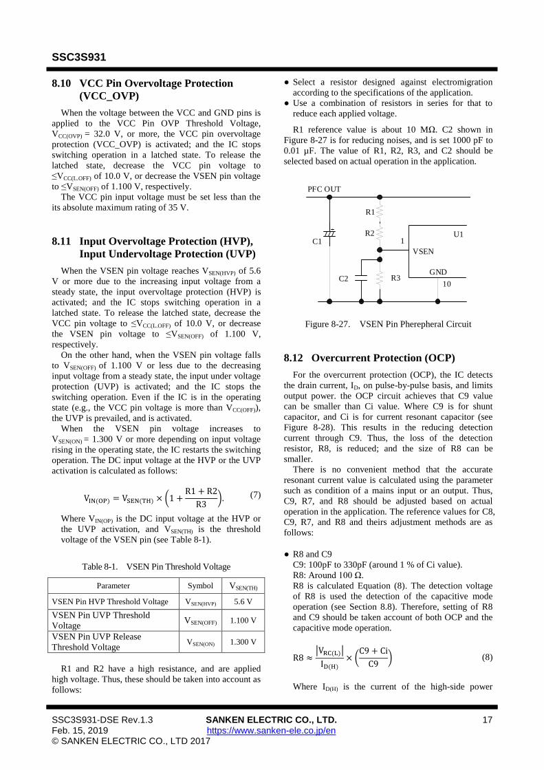
R1 reference value is about 10 MΩ. C2 shown in
Figure 8-27 is for reducing noises, and is set 1000 pF to
0.01 µF. The value of R1, R2, R3, and C2 should be
selected based on actual operation in the application.
10
GND
U1
R3
VSEN
C2
R1
R2C1 1
PFC OUT
Figure 8-27. VSEN Pin Pherepheral Circuit
8.12 Overcurrent Protection (OCP)
For the overcurrent protection (OCP), the IC detects
the drain current, ID, on pulse-by-pulse basis, and limits
output power. the OCP circuit achieves that C9 value
can be smaller than Ci value. Where C9 is for shunt
capacitor, and Ci is for current resonant capacitor (see
Figure 8-28). This results in the reducing detection
current through C9. Thus, the loss of the detection
resistor, R8, is reduced; and the size of R8 can be
smaller.
There is no convenient method that the accurate
resonant current value is calculated using the parameter
such as condition of a mains input or an output. Thus,
C9, R7, and R8 should be adjusted based on actual
operation in the application. The reference values for C8,
C9, R7, and R8 and theirs adjustment methods are as
follows:
● R8 and C9
C9: 100pF to 330pF (around 1 % of Ci value).
R8: Around 100 Ω.
R8 is calculated Equation (8). The detection voltage
of R8 is used the detection of the capacitive mode
operation (see Section 8.8). Therefore, setting of R8
and C9 should be taken account of both OCP and the
capacitive mode operation.
(8)
Where ID(H) is the current of the high-side power
SSC3S931
SSC3S931-DSE Rev.1.3 SANKEN ELECTRIC CO., LTD. 18 Feb. 15, 2019 https://www.sanken-ele.co.jp/en © SANKEN ELECTRIC CO., LTD 2017
MOSFET at an on state, and VRC(L) is the RC Pin
Threshold Voltage (Low) of ±1.90 V
● R7 and C8
They are for high frequency noise reduction.
R7: 100 Ω to 470 Ω
C8: 100 pF to 1000 pF
T1
R7
Cv
CiC9
C8
VS
VGL
VGH
GNDCSS
U115
11
5 7
10
16
I(H)
RC
C6
R8
R6
Q(H)
Q(L)
CL6
C7
Figure 8-28. RC Pin Peripheral Circuit
The OCP operation has two level threshold voltages
as follows:
8.12.1 Overcurrent Protection 1 (OCP1)
This is a first OCP level. When the absolute value of
the RC pin voltage increases to more than |VOC(L) | of
1.90 V, C6 connected to the CSS pin is discharged by
ICSS(L) = 1.8 mA. Thus, the switching frequency increases
to prevent the output power rising. When the absolute
value of the RC pin voltage decreases to |VRC(L)| or less
during the C6 discharge, the C6 discharge is stopped.
8.12.2 Overcurrent Protection 2 (OCP2)
This is a second OCP level. When the absolute value
of the RC pin voltage increases to more than
|VRC(H)| = 2.80 V, the high speed OCP is activated. Then,
the on/off statuses of power MOSFETs are inverted. At
the same time, C6 is discharged by ICSS(H) = 20.5 mA.
Thus, the switching frequency quickly increases to
quickly prevent the output power rising. The OCP2
protects the IC from the exceeding overcurrent caused
by the abnormal condition such as the output shorted.
When the absolute value of the RC pin voltage
decreases to |VRC(H)| or less, the OCP level is transferred
to OCP1 operation.
8.13 Overload Protection (OLP)
Figure 8-29 shows the overload protection (OLP)
waveforms. When increasing of an output power and the
overcurrent protection 1 (OCP1) is activated, the C7
connected to the CL pin is charged by ICL(SRC)1 of −17
μA. Moreover, when the overcurrent protection 2
(OCP2) is activated, the C7 connected to the CL pin is
charged by ICL(SRC)2 of −135 μA. When the CL pin
voltage increases to VCL(OLP) of 4.2 V due to maintaining
the OCP1 or OCP2 operations, the OLP is activated, and
the switching operation stops in a latched state. To
release the latched state, decrease the VCC pin voltage
to ≤VCC(L.OFF) of 10.0 V, or decrease the VSEN pin
voltage to ≤VSEN(OFF) of 1.100 V, respectively.
VCC Pin Voltage
VGH/VGL
0
0
VCC(L.OFF)
VCC(ON)
RC Pin Voltage
CL Pin Voltage
VRC(L)
VRC(L)
VCL(OLP)
0
0
Charged by
ICL(SRC)
VCC(OFF)
Releasing
latched state
Figure 8-29. OLP Waveform
8.14 Optocoupler Open Protection (OOP)
In case the primary side of an optocoupler becomes
open, a feedback current reduction due to the FB pin
voltage rising result in the output voltage increases. To
prevent the status the IC has the optocoupler open
protection (OOP). The OOP is activated at following
condition.
- When the FB pin voltage increases to higher than the
CSS pin voltage, or
- When the FB pin voltage increases to the FB Pin
Open Detection Threshold Voltage, VFB(OOP) = 4.6 V,
or more.
After the OOP activation, C10 connected to the CD
pin is charged by the CD Pin Source Current,
ICD(SRC) = –20 μA. When the CD pin voltage increases to
the CD Pin Threshold Voltage, VCD = 3.0 V, the IC
stops switching operation in a latched state. To release
the latched state, decrease the VCC pin voltage to
≤VCC(L.OFF) of 10.0 V, or decrease the VSEN pin voltage
to ≤VSEN(OFF) of 1.100 V, respectively.
SSC3S931
SSC3S931-DSE Rev.1.3 SANKEN ELECTRIC CO., LTD. 19 Feb. 15, 2019 https://www.sanken-ele.co.jp/en © SANKEN ELECTRIC CO., LTD 2017
The delay time is period until the switching operation
stop from the OOP activation. The maximum delay time,
tDLY_MAX, is calculated by following equation.
(9)
where:
VCD is the CD Pin Threshold Voltage of 3.0 V, CCD is the value of C10 connected to the CD pin
(about 0.1 µF to 2.2 µF), and ICD(SRC) is the CD Pin Source Current of –20 μA.
If C10 = 0.1 µF,
During startup operation (see Section 8.3), the CD pin
voltage increases because C10 is charged. C10 must be
set the value with enough margins. To prevent a startup
failure, C10 must be set enough large value so that the
CD pin voltage is less than 3.0 V during startup period.
In addition, the condition when the soft start period is
longest (e.g., minimum input voltage and maximum
output power) should be taken into account.
8.15 Thermal Shutdown (TSD)
When the junction temperature of the IC reach to the
Thermal Shutdown Temperature Tj(TSD) = 140 °C (min.),
the thermal shutdown (TSD) is activated; and the IC
stops switching operation in a latched state.
To release the latched state, decrease the VCC pin
voltage to ≤VCC(L.OFF) of 10.0 V, or decrease the VSEN
pin voltage to ≤VSEN(OFF) of 1.100 V, respectively.
9. Design Notes
9.1 External Components
Take care to use the proper rating and proper type of
components.
9.1.1 Input and Output Electrolytic
Capacitors
Apply proper derating to a ripple current, a voltage,
and a temperature rise. It is required to use the high
ripple current and low impedance type electrolytic
capacitor that is designed for switch mode power
supplies.
9.1.2 Resonant Transformer
The resonant power supply uses the leakage
inductance of a transformer. Therefore, to reduce the
effect of the eddy current and the skin effect, the wire of
transformer should be used a bundle of fine litz wires.
9.1.3 Current Detection Resistor, ROCP
To reduce the effect of the high frequency switching
current flowing through ROCP, choose the resister of a
low internal inductance type. In addition, its allowable
dissipation should be chosen suitable.
9.1.4 Current Resonant Capacitor, Ci
Since a large resonant current flows through Ci, Ci
should be used a low loss and a high current capability
capacitor such as a polypropylene film capacitor. In
addition, Ci must be taken into account its frequency
characteristic because a high frequency current flows.
9.1.5 Gate Pin Peripheral Circuit
The VGH and VGL pins are gate drive outputs for
external power MOSFETs. These peak source and sink
currents are –540 mA and 1.50 A, respectively.
To make a turn-off speed faster, connect the diode, DS,
as shown in Figure 9-1. When RA and DS is adjusted, the
following contents should be taken into account: the
power losses of power MOSFETs, gate waveforms (for
a ringing reduction caused by a pattern layout, etc.), and
EMI noises. To prevent the malfunctions caused by
steep dv/dt at turn-off of power MOSFETs, connect RGS
of 10 kΩ to 100 kΩ between the Gate and Source pins of
the power MOSFET with a minimal length of PCB
traces. When these gate resistances are adjusted, the gate
SSC3S931
SSC3S931-DSE Rev.1.3 SANKEN ELECTRIC CO., LTD. 20 Feb. 15, 2019 https://www.sanken-ele.co.jp/en © SANKEN ELECTRIC CO., LTD 2017
waveforms should be checked that the dead time is
ensured as shown in Figure 9-2.
DS
RA
RGS
Drain
Source
Gate
Figure 9-1. Power MOSFET Peripheral Circuit
High-side
Gate
Low-side
Gate
Vth(min.)
Vth(min.)
Dead time Dead time
Figure 9-2. Dead Time Confirmation
9.2 PCB Trace Layout and Component
Placement
The PCB circuit design and the component layout
significantly affect a power supply operation, EMI
noises, and power dissipation. Thus, to reduce the
impedance of the high frequency traces on a PCB (see
Figure 9-3), they should be designed as wide trace and
small loop as possible. In addition, ground traces should
be as wide and short as possible so that radiated EMI
levels can be reduced.
Figure 9-3. High Frequency Current Loops
(Hatched Areas)
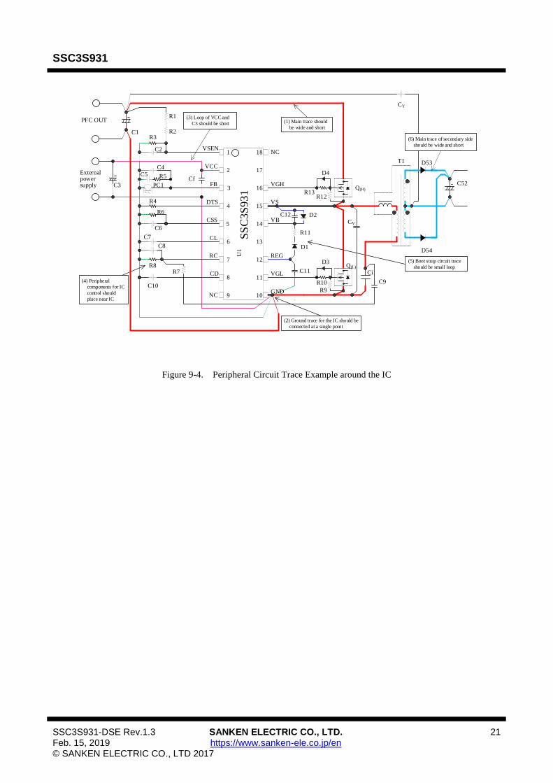
Figure 9-4 shows the circuit design example. The
PCB trace design should be also taken into account as
follows:
1) Main Circuit Trace
The main traces that switching current flows should
be designed as wide trace and small loop as possible.
2) Control Ground Trace
If the large current flows through a control ground, it
may cause varying electric potential of the control
ground; and this may result in the malfunctions of the
IC. Therefore, connect the control ground as close and
short as possible to the GND pin at a single-point
ground (or star ground) that is separated from the
power ground.
3) VCC Trace
The trace for supplying power to the IC should be as
small loop as possible. If C3 and the IC are distant
from each other, a film capacitor Cf (about 0.1 μF to
1.0 μF) should be connected between the VCC and
GND pins with a minimal length of PCB traces.
4) Trace of Peripheral Components for the IC Control
These components should be placed close to the IC,
and be connected to the corresponding pin of the IC
with as short trace as possible.
5) Trace of Bootstrap Circuit Components
These components should be connected to the IC pin
with as short trace as possible. In addition, the loop
for these should be as small as possible.
6) Secondary Side Rectifier Smoothing Circuit Trace
The traces of the rectifier smoothing loops carry the
switching current. Thus it should be designed as wide
trace and small loop as possible.
SSC3S931
SSC3S931-DSE Rev.1.3 SANKEN ELECTRIC CO., LTD. 21 Feb. 15, 2019 https://www.sanken-ele.co.jp/en © SANKEN ELECTRIC CO., LTD 2017
T1
DTS
VSEN
VCC
FB
CSS
CL
CD
RC
NC
NC
VGH
VS
VB
REG
VGL
GND
1
15
16
17
18
4
3
2
U1
SS
C3S
93
1
7
6
5
12
13
14
9
8
10
11
PC1
C1
R1
R2R3
C2
Cf
C4
C5
C6
R6
C7
C8
R8R7 C11
D1
R11
C12 D2
D4
R13R12
Q(H)
Q(L)D3
R10
R9
CV
Ci
C9
D53
D54
C52
CY
(6) Main trace of secondary side
should be wide and short
(1) Main trace should
be wide and short
(2) Ground trace for the IC should be
connected at a single point
(4) Peripheral
components for IC
control should
place near IC
(5) Boot strap circuit trace
should be small loop
R4
C10
PFC OUT
R5External power supply
(3) Loop of VCC and
C3 should be short
C3
Figure 9-4. Peripheral Circuit Trace Example around the IC
SSC3S931
SSC3S931-DSE Rev.1.3 SANKEN ELECTRIC CO., LTD. 22 Feb. 15, 2019 https://www.sanken-ele.co.jp/en © SANKEN ELECTRIC CO., LTD 2017
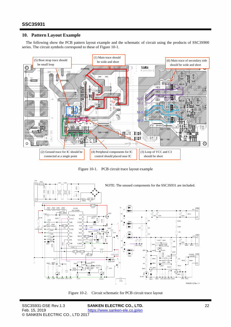
10. Pattern Layout Example
The following show the PCB pattern layout example and the schematic of circuit using the products of SSC3S900
series. The circuit symbols correspond to these of Figure 10-1.
Figure 10-1. PCB circuit trace layout example
VR
101
CX
101
CN1F101
D202
R213
C203
C104
R201 R202 R203 R204
R205C204
R209
C205
C206
C207
R212
D205
R22
5
R22
1
D201
C201
C212
C214
C215
C103
D203D204R215
D206
C225
C209C208
R208R207
R200 C210
Q204
R218 R217
D207
D208
C213PC201 PC202
C216
18
17
16
15
14
13
12
11
10
1
2
3
4
5
6
7
8
9
TH101
T1
L101
C217
Q201
Q202
R206
R10
1R
102
R10
3
L102
CX
102
C10
2C
101
C218
C202
R21
9
R21
4R
211
R23
0
C211
P
D
1
3
6
4
PSA50112_Rev.1.1
CN601
R609C301C308
R302
R301
R306
R307
R310
R303 C305
PC201
Q301
R304
C605
Q601
PC202
D601
R601
R602R610
POWER_
ON/OFFC304
12V
CN401
Q606
R614
R616
R615C606
S1
S2
10
8,9
7
R604
R305
Q602
D301
D302
CN602
R613
C302 C309 C604
24V
S3
S4 D304
D303
14
13
12
D602 R605
R606
R603
R309
R308
J2
J5//J7
J3//J8
J13
R210
J14
J18TR1
J15
R216
J6
J1J9 J23
J11 R22
0
J12
J24
J33
J24
J33
C601
J26
J20,
J30,
J32
C303
J21
J27
J31
J29
J28
VSEN
CL
RC
VCC
FB
DTS
CSS
PL
SB
IC201
SSC3S900
ST
NC
REG
NC
VGH
VS
VB
VGL
GND
Figure 10-2. Circuit schematic for PCB circuit trace layout
Lp
D
(1) Main trace should
be wide and short
(6) Main trace of secondary side
should be wide and short
(5) Boot strap trace should
be small loop
(4) Peripheral components for IC
control should placed near IC
(2) Ground trace for IC should be
connected at a single point
(3) Loop of VCC and C3
should be short
S1-1
S1-2
S2-1
S2-2
NOTE: The unused components for the SSC3S931 are included.
SSC3S931
SSC3S931-DSE Rev.1.3 SANKEN ELECTRIC CO., LTD. 23 Feb. 15, 2019 https://www.sanken-ele.co.jp/en © SANKEN ELECTRIC CO., LTD 2017
Important Notes
● All data, illustrations, graphs, tables and any other information included in this document (the “Information”) as to Sanken’s
products listed herein (the “Sanken Products”) are current as of the date this document is issued. The Information is subject to any
change without notice due to improvement of the Sanken Products, etc. Please make sure to confirm with a Sanken sales
representative that the contents set forth in this document reflect the latest revisions before use.
● The Sanken Products are intended for use as components of general purpose electronic equipment or apparatus (such as home
appliances, office equipment, telecommunication equipment, measuring equipment, etc.). Prior to use of the Sanken Products,
please put your signature, or affix your name and seal, on the specification documents of the Sanken Products and return them to
Sanken. When considering use of the Sanken Products for any applications that require higher reliability (such as transportation
equipment and its control systems, traffic signal control systems or equipment, disaster/crime alarm systems, various safety
devices, etc.), you must contact a Sanken sales representative to discuss the suitability of such use and put your signature, or affix
your name and seal, on the specification documents of the Sanken Products and return them to Sanken, prior to the use of the
Sanken Products. The Sanken Products are not intended for use in any applications that require extremely high reliability such as:
aerospace equipment; nuclear power control systems; and medical equipment or systems, whose failure or malfunction may result
in death or serious injury to people, i.e., medical devices in Class III or a higher class as defined by relevant laws of Japan
(collectively, the “Specific Applications”). Sanken assumes no liability or responsibility whatsoever for any and all damages and
losses that may be suffered by you, users or any third party, resulting from the use of the Sanken Products in the Specific
Applications or in manner not in compliance with the instructions set forth herein. ● In the event of using the Sanken Products by either (i) combining other products or materials or both therewith or (ii) physically,
chemically or otherwise processing or treating or both the same, you must duly consider all possible risks that may result from all
such uses in advance and proceed therewith at your own responsibility. ● Although Sanken is making efforts to enhance the quality and reliability of its products, it is impossible to completely avoid the
occurrence of any failure or defect or both in semiconductor products at a certain rate. You must take, at your own responsibility,
preventative measures including using a sufficient safety design and confirming safety of any equipment or systems in/for which
the Sanken Products are used, upon due consideration of a failure occurrence rate and derating, etc., in order not to cause any
human injury or death, fire accident or social harm which may result from any failure or malfunction of the Sanken Products.
Please refer to the relevant specification documents and Sanken’s official website in relation to derating. ● No anti-radioactive ray design has been adopted for the Sanken Products. ● The circuit constant, operation examples, circuit examples, pattern layout examples, design examples, recommended examples, all
information and evaluation results based thereon, etc., described in this document are presented for the sole purpose of reference of
use of the Sanken Products. ● Sanken assumes no responsibility whatsoever for any and all damages and losses that may be suffered by you, users or any third
party, or any possible infringement of any and all property rights including intellectual property rights and any other rights of you,
users or any third party, resulting from the Information. ● No information in this document can be transcribed or copied or both without Sanken’s prior written consent.
● Regarding the Information, no license, express, implied or otherwise, is granted hereby under any intellectual property rights and
any other rights of Sanken. ● Unless otherwise agreed in writing between Sanken and you, Sanken makes no warranty of any kind, whether express or implied,
including, without limitation, any warranty (i) as to the quality or performance of the Sanken Products (such as implied warranty
of merchantability, and implied warranty of fitness for a particular purpose or special environment), (ii) that any Sanken Product is
delivered free of claims of third parties by way of infringement or the like, (iii) that may arise from course of performance, course
of dealing or usage of trade, and (iv) as to the Information (including its accuracy, usefulness, and reliability). ● In the event of using the Sanken Products, you must use the same after carefully examining all applicable environmental laws and
regulations that regulate the inclusion or use or both of any particular controlled substances, including, but not limited to, the EU
RoHS Directive, so as to be in strict compliance with such applicable laws and regulations. ● You must not use the Sanken Products or the Information for the purpose of any military applications or use, including but not
limited to the development of weapons of mass destruction. In the event of exporting the Sanken Products or the Information, or
providing them for non-residents, you must comply with all applicable export control laws and regulations in each country
including the U.S. Export Administration Regulations (EAR) and the Foreign Exchange and Foreign Trade Act of Japan, and
follow the procedures required by such applicable laws and regulations. ● Sanken assumes no responsibility for any troubles, which may occur during the transportation of the Sanken Products including
the falling thereof, out of Sanken’s distribution network. ● Although Sanken has prepared this document with its due care to pursue the accuracy thereof, Sanken does not warrant that it is
error free and Sanken assumes no liability whatsoever for any and all damages and losses which may be suffered by you resulting
from any possible errors or omissions in connection with the Information. ● Please refer to our official website in relation to general instructions and directions for using the Sanken Products, and refer to the
relevant specification documents in relation to particular precautions when using the Sanken Products.
● All rights and title in and to any specific trademark or tradename belong to Sanken and such original right holder(s).
DSGN-CEZ-16003


![Presentazione standard di PowerPoint · ATLAS Preliminary April 2018 3 Tev, 3.6-37.0 fb 95% CL upper limits Observed Expected < 0.3 ... A TLAS Work in Progress [TeV] DM Simplified](https://img.pdfslide.us/doc/110x75/5f7762c36e1b855f9400dccd/presentazione-standard-di-powerpoint-atlas-preliminary-april-2018-3-tev-36-370.jpg)