Embed Size (px)
Citation preview
Spring 08, Jan 31 . .Spring 08, Jan 31 . . ELEC 7770: Advanced VLSI Design (Agrawal)ELEC 7770: Advanced VLSI Design (Agrawal) 11
ELEC 7770ELEC 7770Advanced VLSI DesignAdvanced VLSI Design
Spring 2008Spring 2008 Timing Simulation and STA Timing Simulation and STA
Vishwani D. AgrawalVishwani D. Agrawal
James J. Danaher ProfessorJames J. Danaher Professor
ECE Department, Auburn University, Auburn, AL 36849ECE Department, Auburn University, Auburn, AL 36849
[email protected]@eng.auburn.eduhttp://www.eng.auburn.edu/~vagrawal/COURSE/E7770_Spr08/course.htmlhttp://www.eng.auburn.edu/~vagrawal/COURSE/E7770_Spr08/course.html
Spring 08, Jan 31 . .Spring 08, Jan 31 . . ELEC 7770: Advanced VLSI Design (Agrawal)ELEC 7770: Advanced VLSI Design (Agrawal) 22
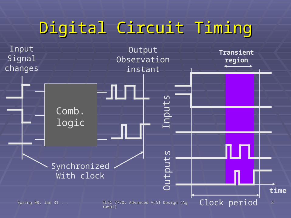
Digital Circuit TimingDigital Circuit Timing
Inpu
tsO
utpu
ts
time
Transientregion
Clock period
Comb.logic
OutputObservation
instant
InputSignal
changes
SynchronizedWith clock
Spring 08, Jan 31 . .Spring 08, Jan 31 . . ELEC 7770: Advanced VLSI Design (Agrawal)ELEC 7770: Advanced VLSI Design (Agrawal) 33
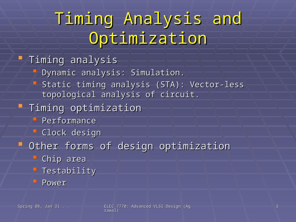
Timing Analysis and OptimizationTiming Analysis and Optimization
Timing analysisTiming analysis Dynamic analysis: Simulation.Dynamic analysis: Simulation. Static timing analysis (STA): Vector-less topological analysis of Static timing analysis (STA): Vector-less topological analysis of
circuit.circuit.
Timing optimizationTiming optimization PerformancePerformance Clock designClock design
Other forms of design optimizationOther forms of design optimization Chip areaChip area TestabilityTestability PowerPower
Spring 08, Jan 31 . .Spring 08, Jan 31 . . ELEC 7770: Advanced VLSI Design (Agrawal)ELEC 7770: Advanced VLSI Design (Agrawal) 44
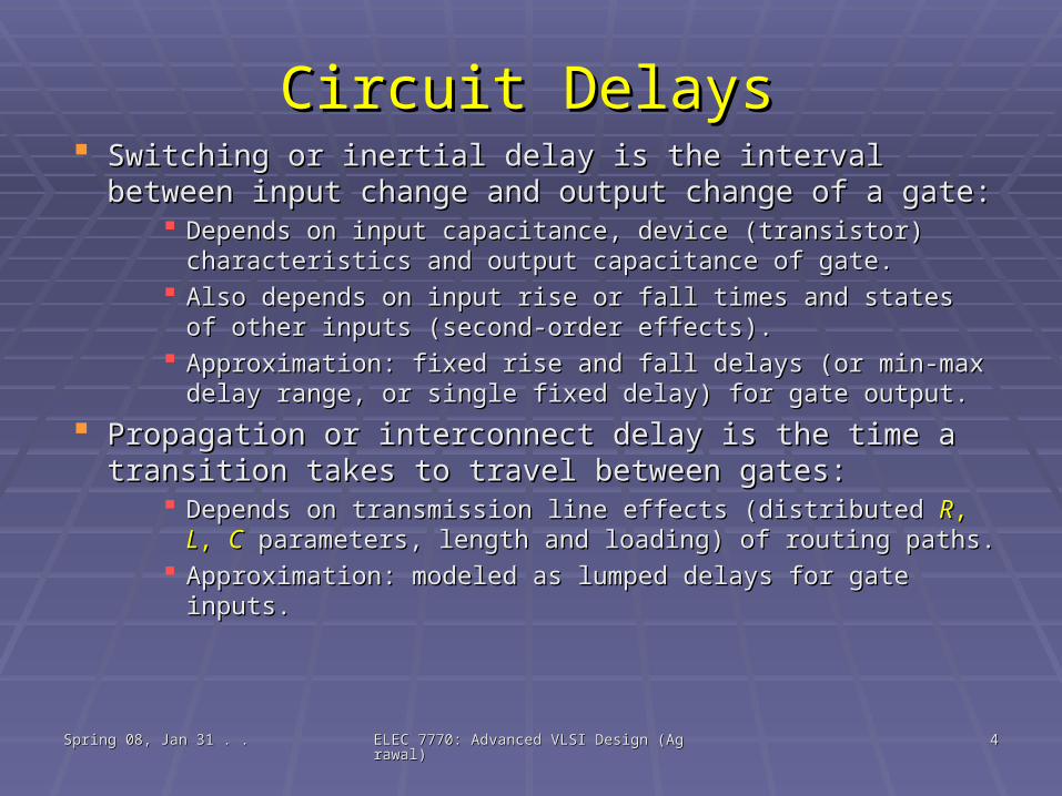
Circuit DelaysCircuit Delays Switching or inertial delay is the interval between input Switching or inertial delay is the interval between input
change and output change of a gate:change and output change of a gate: Depends on input capacitance, device (transistor) Depends on input capacitance, device (transistor)
characteristics and output capacitance of gate.characteristics and output capacitance of gate. Also depends on input rise or fall times and states of other Also depends on input rise or fall times and states of other
inputs (second-order effects).inputs (second-order effects). Approximation: fixed rise and fall delays (or min-max delay Approximation: fixed rise and fall delays (or min-max delay
range, or single fixed delay) for gate output.range, or single fixed delay) for gate output.
Propagation or interconnect delay is the time a transition Propagation or interconnect delay is the time a transition takes to travel between gates:takes to travel between gates:
Depends on transmission line effects (distributed Depends on transmission line effects (distributed RR, , LL, , CC parameters, length and loading) of routing paths.parameters, length and loading) of routing paths.
Approximation: modeled as lumped delays for gate inputs.Approximation: modeled as lumped delays for gate inputs.
Spring 08, Jan 31 . .Spring 08, Jan 31 . . ELEC 7770: Advanced VLSI Design (Agrawal)ELEC 7770: Advanced VLSI Design (Agrawal) 55
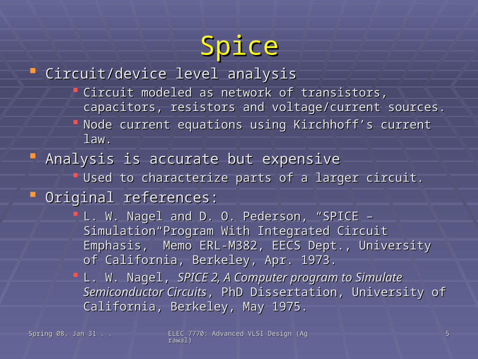
SpiceSpice Circuit/device level analysisCircuit/device level analysis
Circuit modeled as network of transistors, capacitors, Circuit modeled as network of transistors, capacitors, resistors and voltage/current sources.resistors and voltage/current sources.
Node current equations using Kirchhoff’s current law.Node current equations using Kirchhoff’s current law.
Analysis is accurate but expensiveAnalysis is accurate but expensive Used to characterize parts of a larger circuit.Used to characterize parts of a larger circuit.
Original references:Original references: L. W. Nagel and D. O. Pederson, “SPICE – Simulation L. W. Nagel and D. O. Pederson, “SPICE – Simulation
Program With Integrated Circuit Emphasis,” Memo ERL-Program With Integrated Circuit Emphasis,” Memo ERL-M382, EECS Dept., University of California, Berkeley, Apr. M382, EECS Dept., University of California, Berkeley, Apr. 1973.1973.
L. W. Nagel, L. W. Nagel, SPICE 2, A Computer program to Simulate SPICE 2, A Computer program to Simulate Semiconductor CircuitsSemiconductor Circuits, PhD Dissertation, University of , PhD Dissertation, University of California, Berkeley, May 1975.California, Berkeley, May 1975.
Spring 08, Jan 31 . .Spring 08, Jan 31 . . ELEC 7770: Advanced VLSI Design (Agrawal)ELEC 7770: Advanced VLSI Design (Agrawal) 66
Ca
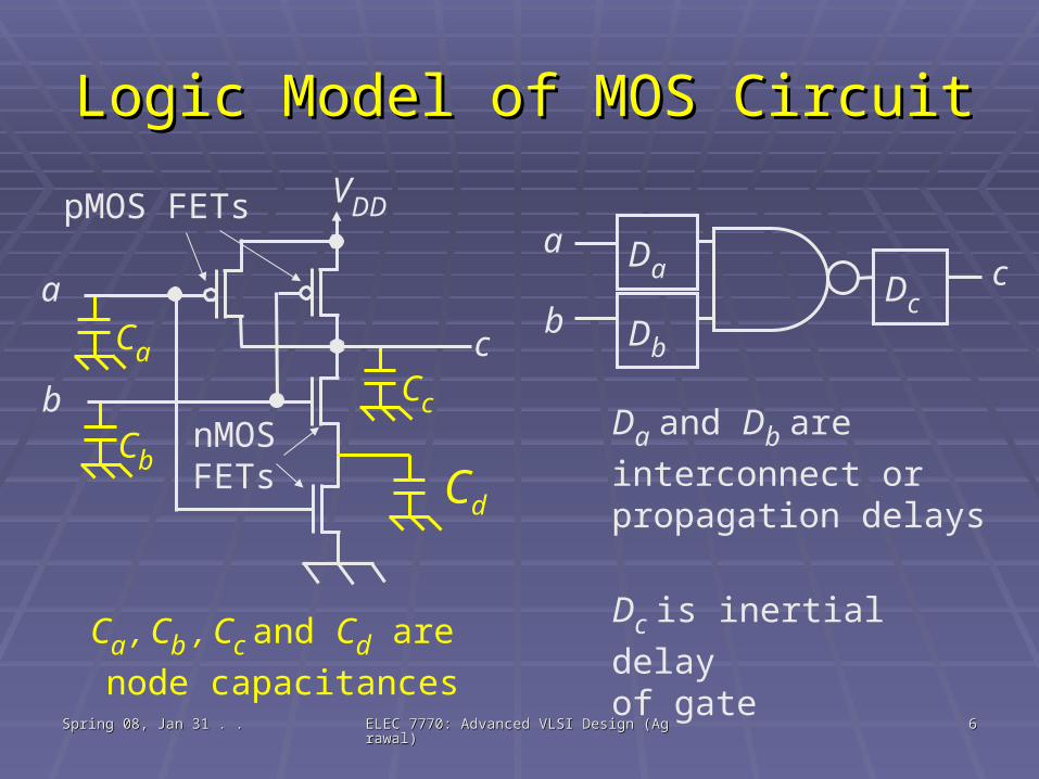
Logic Model of MOS CircuitLogic Model of MOS Circuit
Cc
Cb
VDD
a
b
c
pMOS FETs
nMOSFETs
Ca , Cb , Cc and Cd are
node capacitances
Dc
Da ca
b
Da and Db are
interconnect or propagation delays
Dc is inertial delay
of gate
Db
Cd
Spring 08, Jan 31 . .Spring 08, Jan 31 . . ELEC 7770: Advanced VLSI Design (Agrawal)ELEC 7770: Advanced VLSI Design (Agrawal) 77
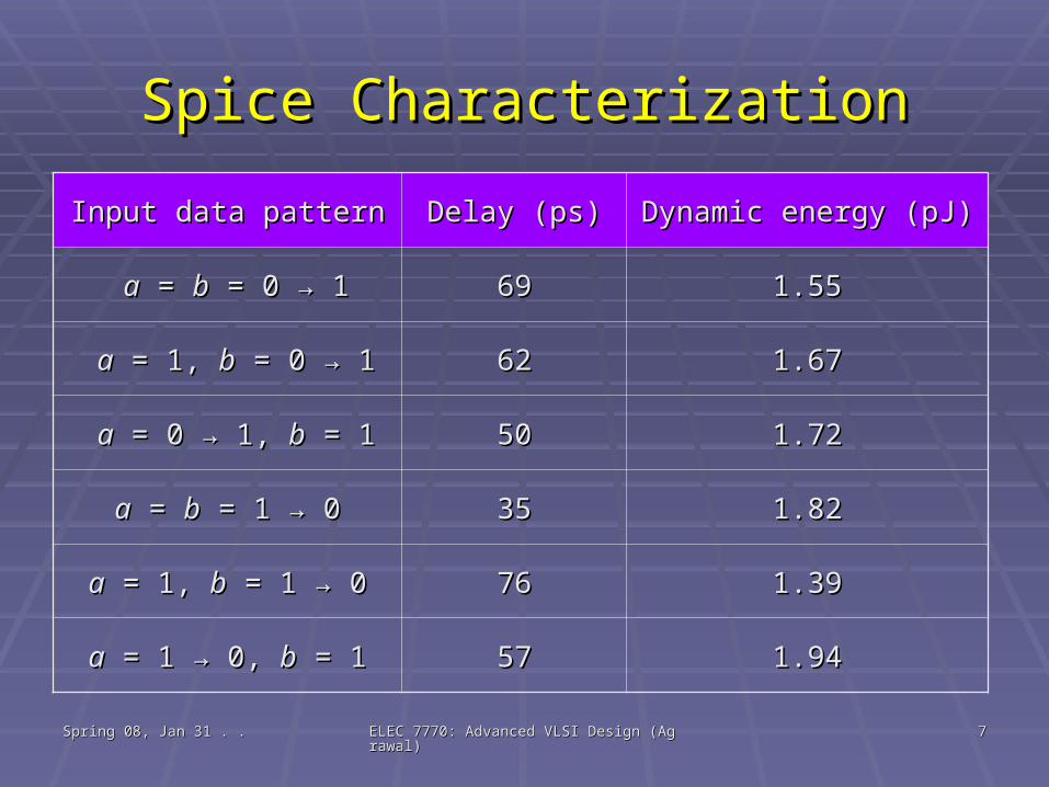
Spice CharacterizationSpice Characterization
Input data patternInput data pattern Delay (ps)Delay (ps) Dynamic energy (pJ)Dynamic energy (pJ)
aa = = bb = 0 → 1 = 0 → 1 6969 1.551.55
aa = 1, = 1, bb = 0 → 1 = 0 → 1 6262 1.671.67
aa = 0 → 1, = 0 → 1, bb = 1 = 1 5050 1.721.72
aa = = bb = 1 → 0 = 1 → 0 3535 1.821.82
aa = 1, = 1, bb = 1 → 0 = 1 → 0 7676 1.391.39
aa = 1 → 0, = 1 → 0, bb = 1 = 1 5757 1.941.94
Spring 08, Jan 31 . .Spring 08, Jan 31 . . ELEC 7770: Advanced VLSI Design (Agrawal)ELEC 7770: Advanced VLSI Design (Agrawal) 88
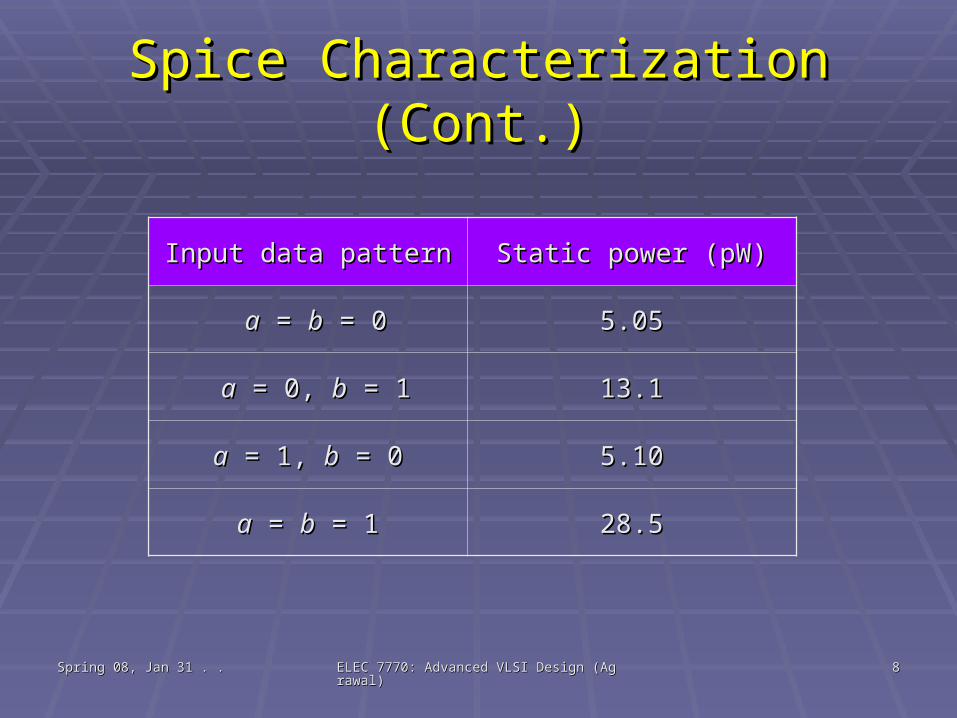
Spice Characterization (Cont.)Spice Characterization (Cont.)
Input data patternInput data pattern Static power (pW)Static power (pW)
aa = = bb = 0 = 0 5.055.05
aa = 0, = 0, bb = 1 = 1 13.113.1
aa = 1, = 1, bb = 0 = 0 5.105.10
aa = = bb = 1 = 1 28.528.5
Spring 08, Jan 31 . .Spring 08, Jan 31 . . ELEC 7770: Advanced VLSI Design (Agrawal)ELEC 7770: Advanced VLSI Design (Agrawal) 99
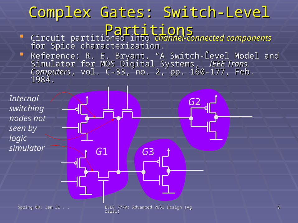
Complex Gates: Switch-Level PartitionsComplex Gates: Switch-Level Partitions Circuit partitioned into Circuit partitioned into channel-connected componentschannel-connected components for Spice for Spice
characterization.characterization. Reference: R. E. Bryant, “A Switch-Level Model and Simulator for Reference: R. E. Bryant, “A Switch-Level Model and Simulator for
MOS Digital Systems,” MOS Digital Systems,” IEEE Trans. ComputersIEEE Trans. Computers, vol. C-33, no. 2, pp. , vol. C-33, no. 2, pp. 160-177, Feb. 1984.160-177, Feb. 1984.
G1
G2
G3
Internal switching nodes not seen by logic simulator
Spring 08, Jan 31 . .Spring 08, Jan 31 . . ELEC 7770: Advanced VLSI Design (Agrawal)ELEC 7770: Advanced VLSI Design (Agrawal) 1010
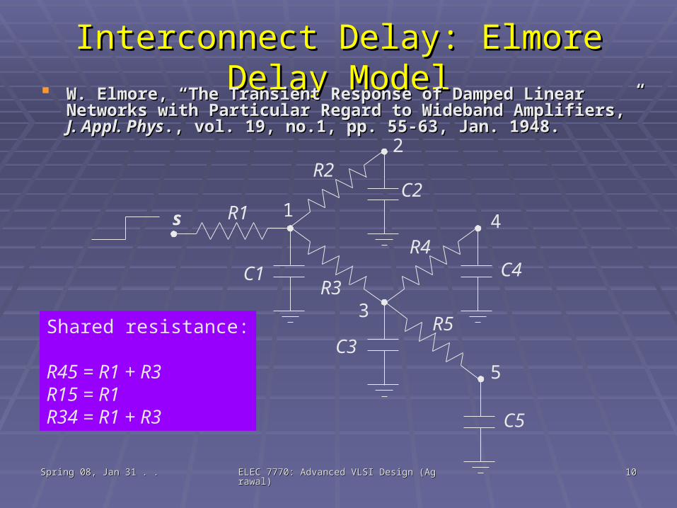
Interconnect Delay: Elmore Delay ModelInterconnect Delay: Elmore Delay Model W. Elmore, “The Transient Response of Damped Linear Networks with W. Elmore, “The Transient Response of Damped Linear Networks with
Particular Regard to Wideband Amplifiers,” Particular Regard to Wideband Amplifiers,” J. Appl. PhysJ. Appl. Phys., vol. 19, ., vol. 19, no.1, pp. 55-63, Jan. 1948.no.1, pp. 55-63, Jan. 1948.
s 1
2
3
4
5
R1
R2
R3
R4
R5
C1
C2
C3
C5
C4
Shared resistance:
R45 = R1 + R3R15 = R1R34 = R1 + R3
Spring 08, Jan 31 . .Spring 08, Jan 31 . . ELEC 7770: Advanced VLSI Design (Agrawal)ELEC 7770: Advanced VLSI Design (Agrawal) 1111
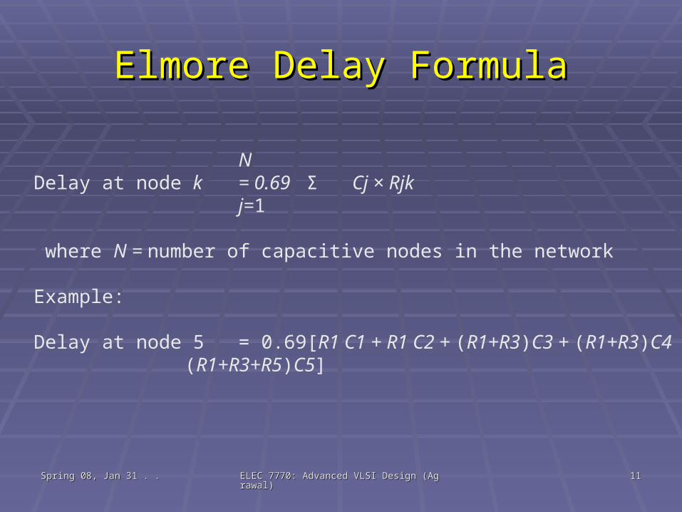
Elmore Delay FormulaElmore Delay Formula
NDelay at node k = 0.69 Σ Cj × Rjk
j=1
where N = number of capacitive nodes in the network
Example:
Delay at node 5 = 0.69[R1 C1 + R1 C2 + (R1+R3)C3 + (R1+R3)C4 (R1+R3+R5)C5]
Spring 08, Jan 31 . .Spring 08, Jan 31 . . ELEC 7770: Advanced VLSI Design (Agrawal)ELEC 7770: Advanced VLSI Design (Agrawal) 1212
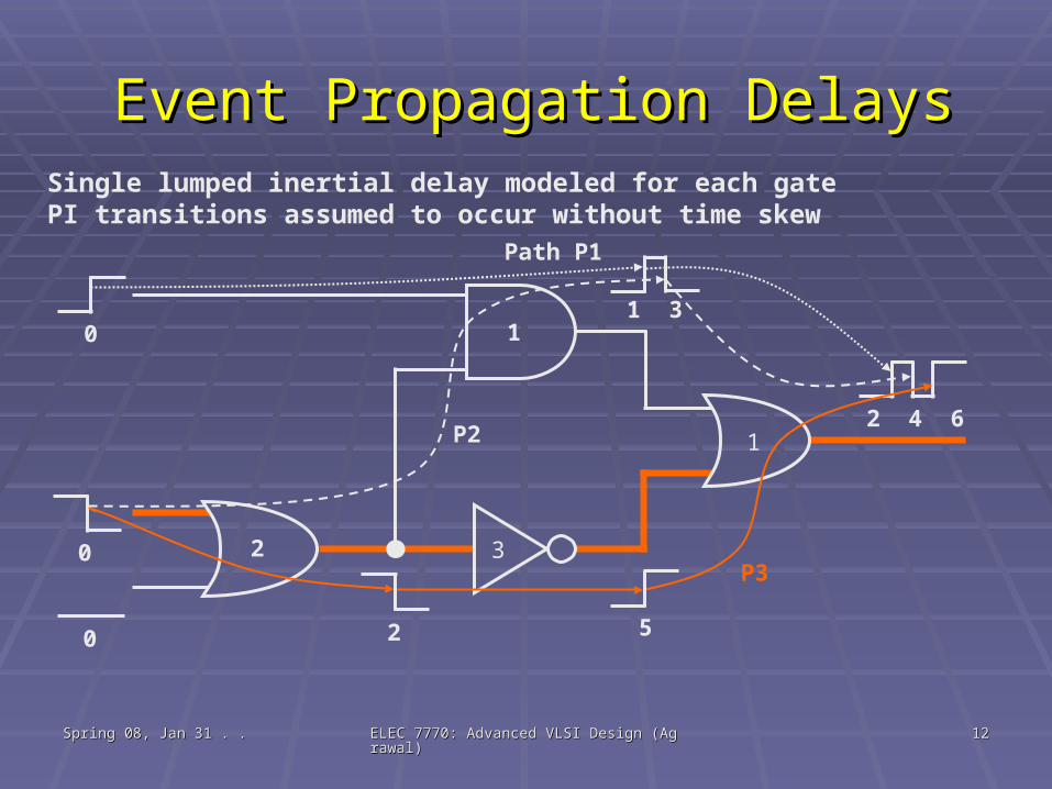
Event Propagation DelaysEvent Propagation Delays
2 4 61
1 3
5
3
10
0
0
2
2
Path P1
P2
P3
Single lumped inertial delay modeled for each gatePI transitions assumed to occur without time skew
Spring 08, Jan 31 . .Spring 08, Jan 31 . . ELEC 7770: Advanced VLSI Design (Agrawal)ELEC 7770: Advanced VLSI Design (Agrawal) 1313
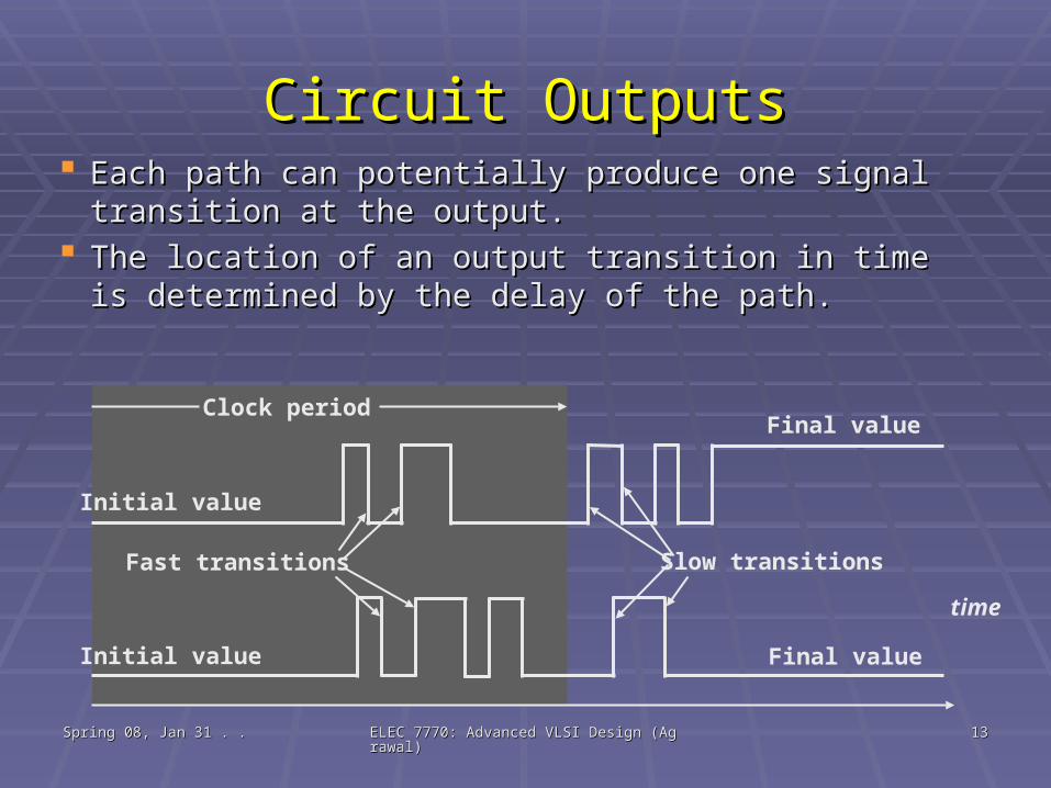
Circuit OutputsCircuit Outputs Each path can potentially produce one signal Each path can potentially produce one signal
transition at the output.transition at the output. The location of an output transition in time is The location of an output transition in time is
determined by the delay of the path.determined by the delay of the path.
Initial value
Initial value
Final value
Final value
Clock period
Fast transitions Slow transitions
time
Spring 08, Jan 31 . .Spring 08, Jan 31 . . ELEC 7770: Advanced VLSI Design (Agrawal)ELEC 7770: Advanced VLSI Design (Agrawal) 1414
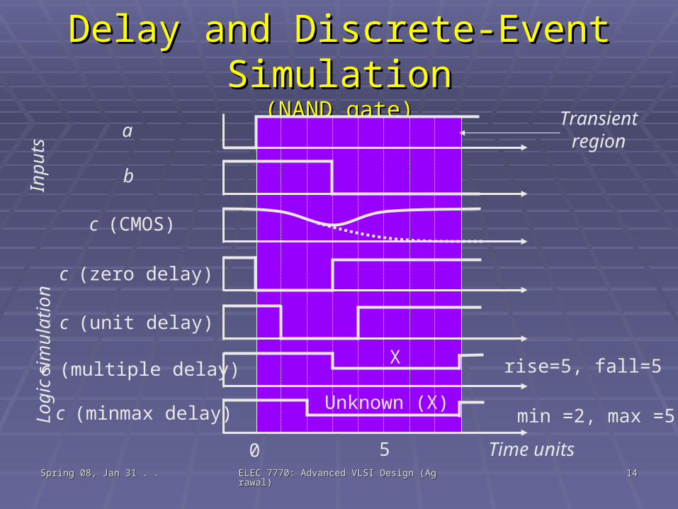
Delay and Discrete-Event SimulationDelay and Discrete-Event Simulation(NAND gate)(NAND gate)
b
a
c (CMOS)
Time units 0 5
c (zero delay)
c (unit delay)
c (multiple delay)
c (minmax delay)
Inp
uts
Log
ic s
imul
atio
n
min =2, max =5
rise=5, fall=5
Transient region
Unknown (X)
X
Spring 08, Jan 31 . .Spring 08, Jan 31 . . ELEC 7770: Advanced VLSI Design (Agrawal)ELEC 7770: Advanced VLSI Design (Agrawal) 1515
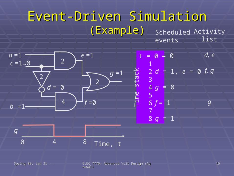
Event-Driven SimulationEvent-Driven Simulation(Example)(Example)
2
2
4
2
a =1
b =1
c =1→0
d = 0
e =1
f =0
g =1
Time, t 0 4 8
g
t = 0 12345678
Scheduledevents
c = 0
d = 1, e = 0
g = 0
f = 1
g = 1
Activitylist
d, e
f, g
gTim
e s
tack
Spring 08, Jan 31 . .Spring 08, Jan 31 . . ELEC 7770: Advanced VLSI Design (Agrawal)ELEC 7770: Advanced VLSI Design (Agrawal) 1616
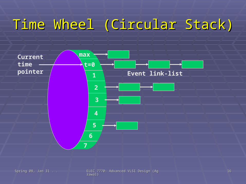
Time Wheel (Circular Stack)Time Wheel (Circular Stack)
t=0
1
2
3
4
5
6
7
maxCurrenttimepointer Event link-list
Spring 08, Jan 31 . .Spring 08, Jan 31 . . ELEC 7770: Advanced VLSI Design (Agrawal)ELEC 7770: Advanced VLSI Design (Agrawal) 1717
Timing Design and Delay TestTiming Design and Delay Test Timing simulation:Timing simulation:
Critical paths are identified by static (vector-less) Critical paths are identified by static (vector-less) timing analysis tools like timing analysis tools like PrimetimePrimetime (Synopsys). (Synopsys).
Timing or circuit-level simulation using designer-Timing or circuit-level simulation using designer-generated functional vectors verifies the design.generated functional vectors verifies the design.
Layout optimization: Critical path data are used in Layout optimization: Critical path data are used in placement and routing. Delay parameter placement and routing. Delay parameter extraction, timing simulation and layout are extraction, timing simulation and layout are repeated for iterative improvement.repeated for iterative improvement.
Testing: Some form of at-speed test is necessary. Testing: Some form of at-speed test is necessary. Critical paths and all gate transition delays are Critical paths and all gate transition delays are tested. tested.
Spring 08, Jan 31 . .Spring 08, Jan 31 . . ELEC 7770: Advanced VLSI Design (Agrawal)ELEC 7770: Advanced VLSI Design (Agrawal) 1818
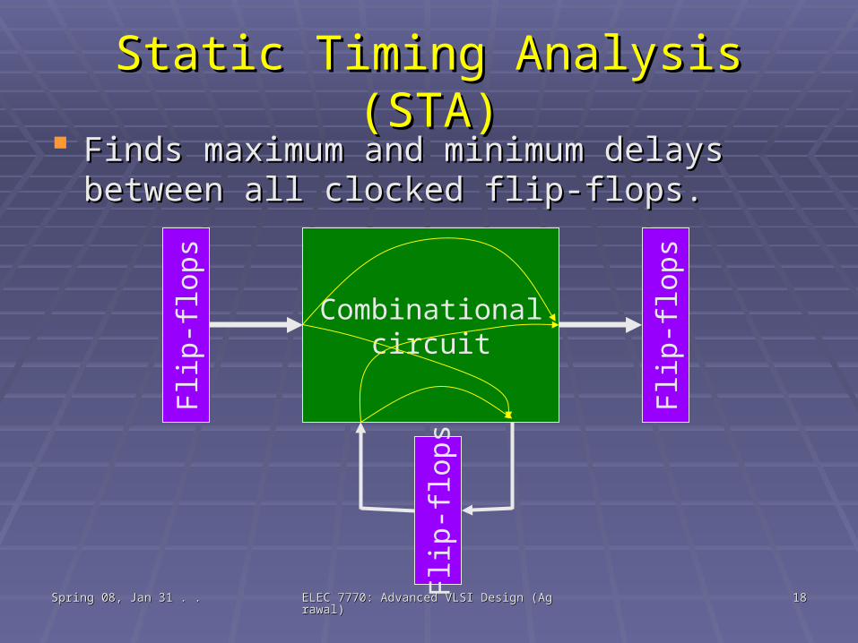
Static Timing Analysis (STA)Static Timing Analysis (STA) Finds maximum and minimum delays between Finds maximum and minimum delays between
all clocked flip-flops.all clocked flip-flops.
Combinationalcircuit
Flip
-flo
ps
Flip
-flo
ps
Flip
-flo
ps
Spring 08, Jan 31 . .Spring 08, Jan 31 . . ELEC 7770: Advanced VLSI Design (Agrawal)ELEC 7770: Advanced VLSI Design (Agrawal) 1919
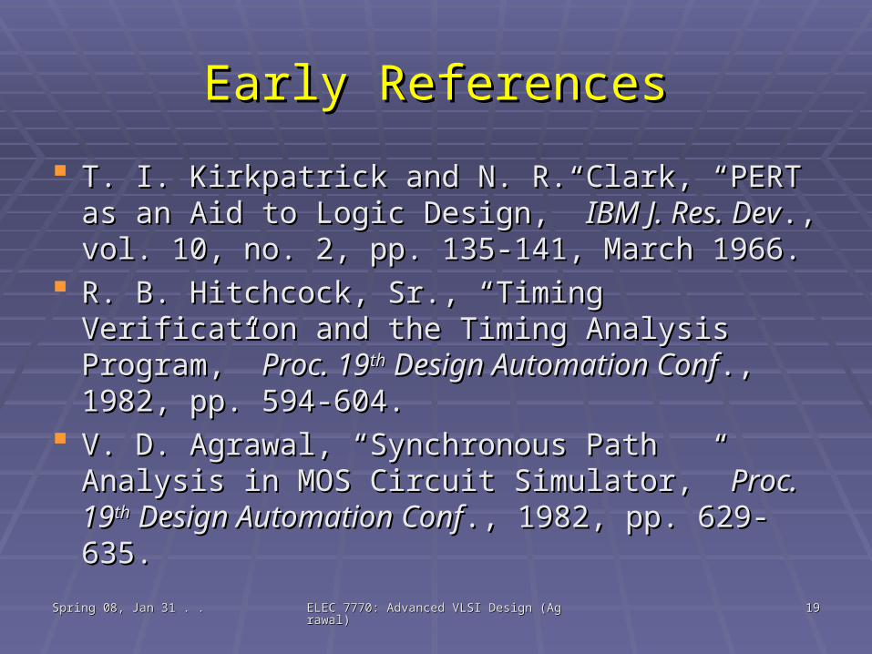
Early ReferencesEarly References
T. I. Kirkpatrick and N. R. Clark, “PERT as an T. I. Kirkpatrick and N. R. Clark, “PERT as an Aid to Logic Design,” Aid to Logic Design,” IBM J. Res. DevIBM J. Res. Dev., vol. 10, ., vol. 10, no. 2, pp. 135-141, March 1966.no. 2, pp. 135-141, March 1966.
R. B. Hitchcock, Sr., “Timing Verification and the R. B. Hitchcock, Sr., “Timing Verification and the Timing Analysis Program,” Timing Analysis Program,” Proc. 19Proc. 19thth Design Design Automation ConfAutomation Conf., 1982, pp. 594-604.., 1982, pp. 594-604.
V. D. Agrawal, “Synchronous Path Analysis in V. D. Agrawal, “Synchronous Path Analysis in MOS Circuit Simulator,” MOS Circuit Simulator,” Proc. 19Proc. 19thth Design Design Automation ConfAutomation Conf., 1982, pp. 629-635.., 1982, pp. 629-635.
Spring 08, Jan 31 . .Spring 08, Jan 31 . . ELEC 7770: Advanced VLSI Design (Agrawal)ELEC 7770: Advanced VLSI Design (Agrawal) 2020
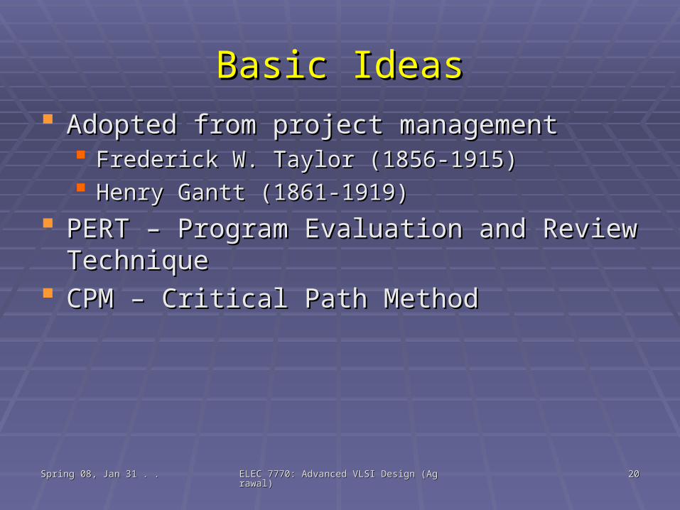
Basic IdeasBasic Ideas Adopted from project managementAdopted from project management
Frederick W. Taylor (1856-1915)Frederick W. Taylor (1856-1915) Henry Gantt (1861-1919)Henry Gantt (1861-1919)
PERT – Program Evaluation and Review PERT – Program Evaluation and Review TechniqueTechnique
CPM – Critical Path MethodCPM – Critical Path Method
Spring 08, Jan 31 . .Spring 08, Jan 31 . . ELEC 7770: Advanced VLSI Design (Agrawal)ELEC 7770: Advanced VLSI Design (Agrawal) 2121
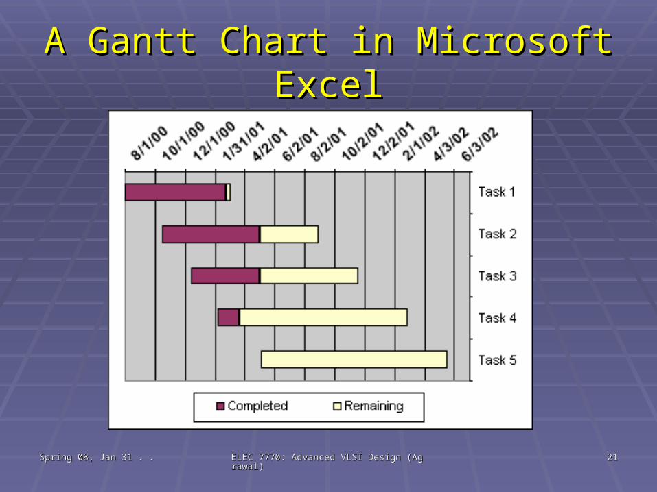
A Gantt Chart in Microsoft ExcelA Gantt Chart in Microsoft Excel
Spring 08, Jan 31 . .Spring 08, Jan 31 . . ELEC 7770: Advanced VLSI Design (Agrawal)ELEC 7770: Advanced VLSI Design (Agrawal) 2222
Using a Gantt ChartUsing a Gantt Chart
Track progress of subtasks and project.Track progress of subtasks and project. Assess resource needs as a function of time.Assess resource needs as a function of time.
Spring 08, Jan 31 . .Spring 08, Jan 31 . . ELEC 7770: Advanced VLSI Design (Agrawal)ELEC 7770: Advanced VLSI Design (Agrawal) 2323
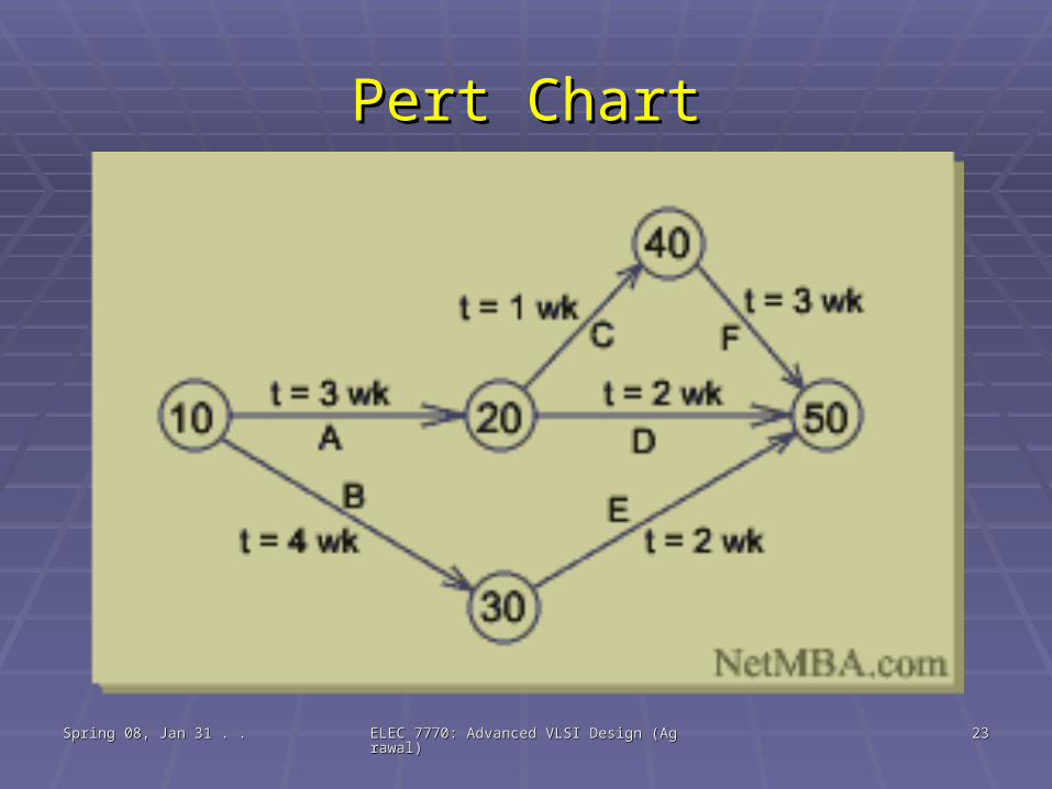
Pert ChartPert Chart
Spring 08, Jan 31 . .Spring 08, Jan 31 . . ELEC 7770: Advanced VLSI Design (Agrawal)ELEC 7770: Advanced VLSI Design (Agrawal) 2424
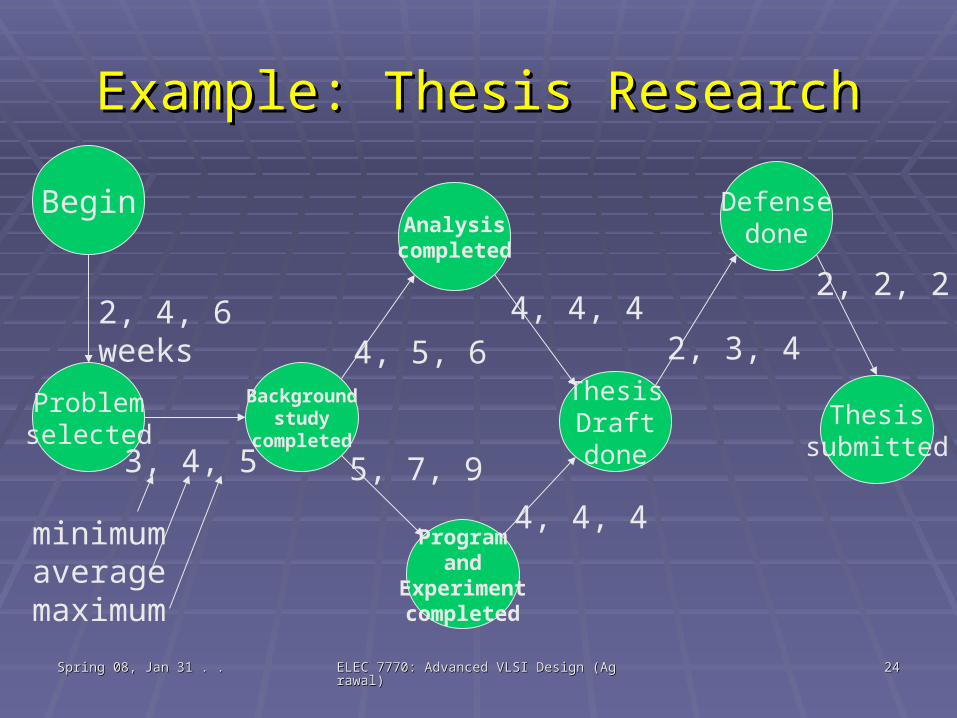
Example: Thesis ResearchExample: Thesis Research
Begin
Problemselected
Backgroundstudy
completed
Programand
Experimentcompleted
Analysiscompleted
ThesisDraftdone
Defensedone
Thesissubmitted
2, 4, 6 weeks
3, 4, 5
4, 5, 6
5, 7, 9
4, 4, 4
4, 4, 4
2, 3, 4
2, 2, 2
minimumaveragemaximum
Spring 08, Jan 31 . .Spring 08, Jan 31 . . ELEC 7770: Advanced VLSI Design (Agrawal)ELEC 7770: Advanced VLSI Design (Agrawal) 2525
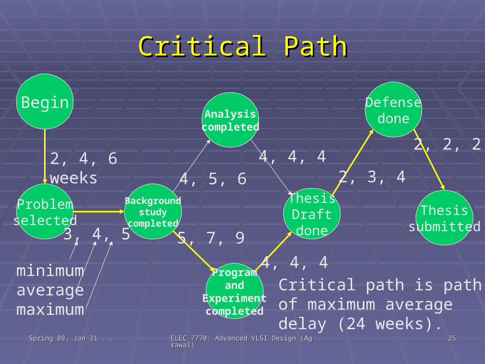
Critical PathCritical Path
Begin
Problemselected
Backgroundstudy
completed
Programand
Experimentcompleted
Analysiscompleted
ThesisDraftdone
Defensedone
Thesissubmitted
2, 4, 6 weeks
3, 4, 5
4, 5, 6
5, 7, 9
4, 4, 4
4, 4, 4
2, 3, 4
2, 2, 2
minimumaveragemaximum
Critical path is pathof maximum averagedelay (24 weeks).
Spring 08, Jan 31 . .Spring 08, Jan 31 . . ELEC 7770: Advanced VLSI Design (Agrawal)ELEC 7770: Advanced VLSI Design (Agrawal) 2626
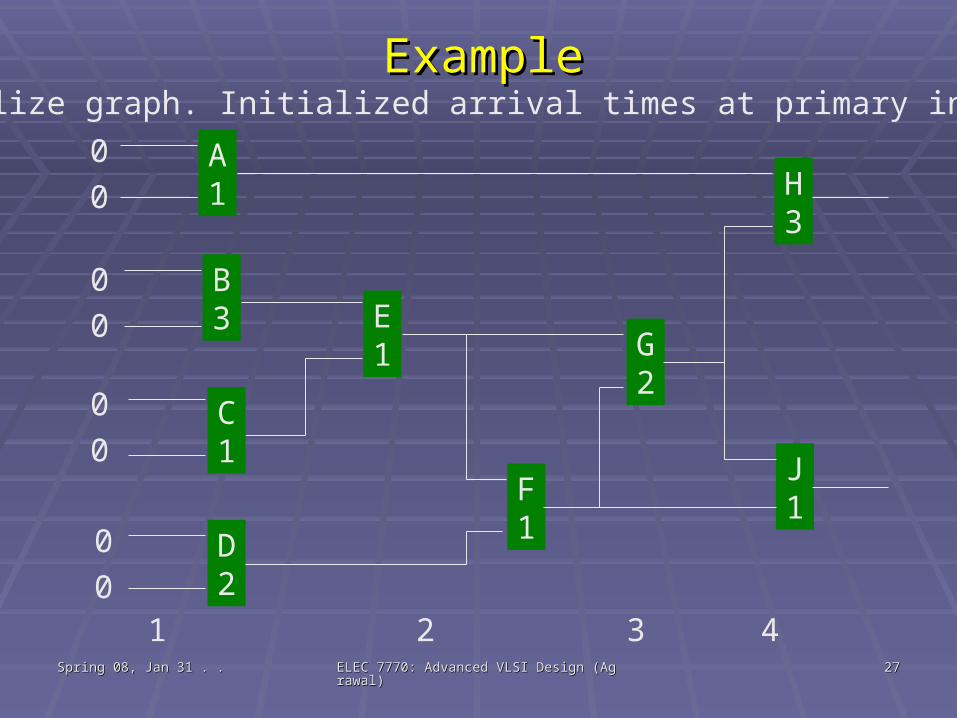
A Basic Timing Analysis AlgorithmA Basic Timing Analysis Algorithm Combinational logic.Combinational logic. Circuit represented as an acyclic directed graph Circuit represented as an acyclic directed graph
(DAG).(DAG). Gates characterized by delays.Gates characterized by delays.
Spring 08, Jan 31 . .Spring 08, Jan 31 . . ELEC 7770: Advanced VLSI Design (Agrawal)ELEC 7770: Advanced VLSI Design (Agrawal) 2727
ExampleExample
A1
B3
D2
E1
F1
J1
G2
H3
0
0
0
0
0
0
0
0
Levelize graph. Initialized arrival times at primary inputs.
Level 0 1 2 3 4 5
C1
Spring 08, Jan 31 . .Spring 08, Jan 31 . . ELEC 7770: Advanced VLSI Design (Agrawal)ELEC 7770: Advanced VLSI Design (Agrawal) 2828
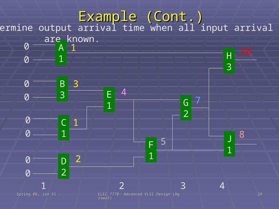
Example (Cont.)Example (Cont.)
A1
B3
C1
D2
E1
F1
J1
G2
H3
0
0
0
0
0
0
0
0
Determine output arrival time when all input arrival times are known.
1
3
1
2
4
5
7
10
8
Level 0 1 2 3 4 5
Spring 08, Jan 31 . .Spring 08, Jan 31 . . ELEC 7770: Advanced VLSI Design (Agrawal)ELEC 7770: Advanced VLSI Design (Agrawal) 2929
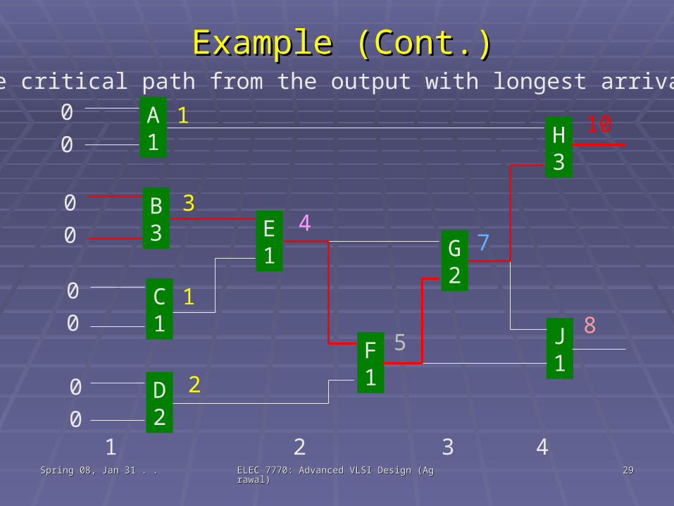
Example (Cont.)Example (Cont.)
A1
B3
C1
D2
E1
F1
J1
G2
H3
0
0
0
0
0
0
0
0
Trace critical path from the output with longest arrival time.
1
3
1
2
4
5
7
10
8
Level 0 1 2 3 4 5
Spring 08, Jan 31 . .Spring 08, Jan 31 . . ELEC 7770: Advanced VLSI Design (Agrawal)ELEC 7770: Advanced VLSI Design (Agrawal) 3030
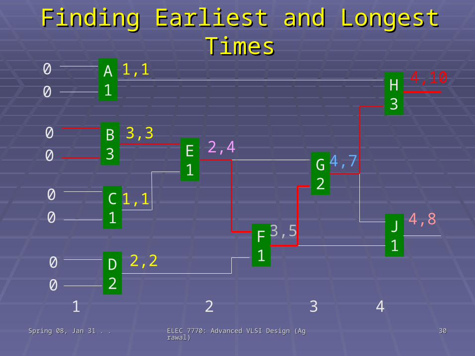
Finding Earliest and Longest TimesFinding Earliest and Longest Times
A1
B3
C1
D2
E1
F1
J1
G2
H3
0
0
0
0
0
0
0
0
1,1
3,3
1,1
2,2
2,4
3,5
4,7
4,10
4,8
Level 0 1 2 3 4 5
Spring 08, Jan 31 . .Spring 08, Jan 31 . . ELEC 7770: Advanced VLSI Design (Agrawal)ELEC 7770: Advanced VLSI Design (Agrawal) 3131
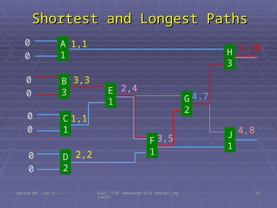
Shortest and Longest PathsShortest and Longest Paths
A1
B3
C1
D2
F1
J1
G2
H3
0
0
0
0
0
0
0
0
1,1
3,3
1,1
2,2
2,4
3,5
4,7
4,10
4,8
E1
Spring 08, Jan 31 . .Spring 08, Jan 31 . . ELEC 7770: Advanced VLSI Design (Agrawal)ELEC 7770: Advanced VLSI Design (Agrawal) 3232
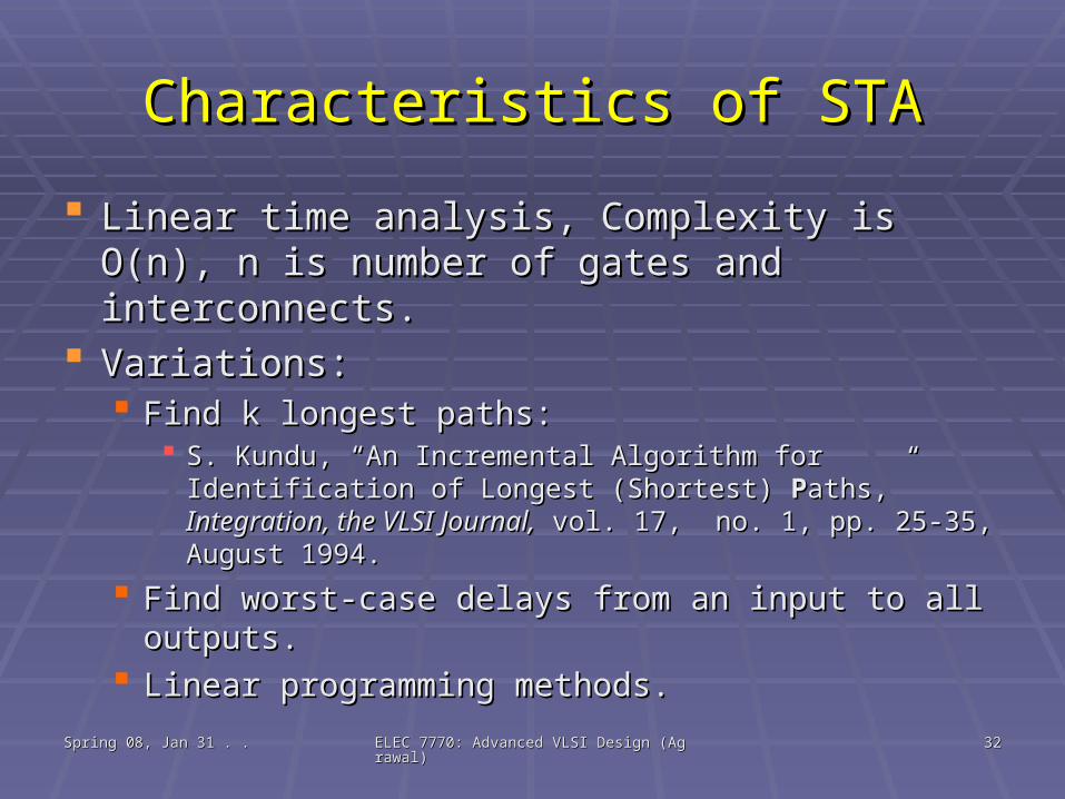
Characteristics of STACharacteristics of STA
Linear time analysis, Complexity is O(n), n is Linear time analysis, Complexity is O(n), n is number of gates and interconnects.number of gates and interconnects.
Variations:Variations: Find k longest paths:Find k longest paths:
S. Kundu, “An Incremental Algorithm for Identification of S. Kundu, “An Incremental Algorithm for Identification of Longest (Shortest)Longest (Shortest) P Paths,”aths,” Integration, the VLSI Journal,Integration, the VLSI Journal, vol. vol. 17, no. 1, pp. 25-35, August 1994.17, no. 1, pp. 25-35, August 1994.
Find worst-case delays from an input to all outputs.Find worst-case delays from an input to all outputs. Linear programming methods.Linear programming methods.
Spring 08, Jan 31 . .Spring 08, Jan 31 . . ELEC 7770: Advanced VLSI Design (Agrawal)ELEC 7770: Advanced VLSI Design (Agrawal) 3333
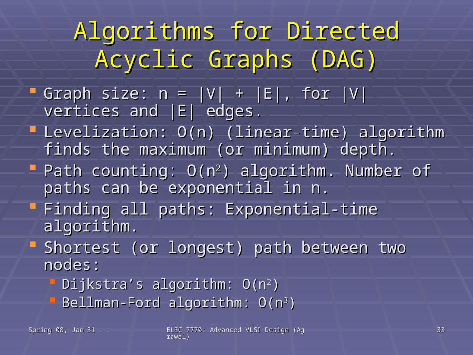
Algorithms for Directed Acyclic Graphs Algorithms for Directed Acyclic Graphs (DAG)(DAG)
Graph size: n = |V| + |E|, for |V| vertices and |E| Graph size: n = |V| + |E|, for |V| vertices and |E| edges.edges.
Levelization: O(n) (linear-time) algorithm finds Levelization: O(n) (linear-time) algorithm finds the maximum (or minimum) depth.the maximum (or minimum) depth.
Path counting: O(nPath counting: O(n22) algorithm. Number of paths ) algorithm. Number of paths can be exponential in n.can be exponential in n.
Finding all paths: Exponential-time algorithm.Finding all paths: Exponential-time algorithm. Shortest (or longest) path between two nodes:Shortest (or longest) path between two nodes:
Dijkstra’s algorithm: O(nDijkstra’s algorithm: O(n22)) Bellman-Ford algorithm: O(nBellman-Ford algorithm: O(n33))
Spring 08, Jan 31 . .Spring 08, Jan 31 . . ELEC 7770: Advanced VLSI Design (Agrawal)ELEC 7770: Advanced VLSI Design (Agrawal) 3434
ReferencesReferences Delay modeling, simulation and testing:Delay modeling, simulation and testing:
M. L. Bushnell and V. D. Agrawal, M. L. Bushnell and V. D. Agrawal, Essentials of Electronic Essentials of Electronic Testing for Digital, Memory and Mixed-Signal VLSI CircuitsTesting for Digital, Memory and Mixed-Signal VLSI Circuits, , Springer, 2000.Springer, 2000.
Analysis and Design:Analysis and Design: G. De Micheli, G. De Micheli, Synthesis and Optimization of Digital CircuitsSynthesis and Optimization of Digital Circuits, ,
McGraw-Hill, 1994.McGraw-Hill, 1994. N. Maheshwari and S. S. Sapatnekar, N. Maheshwari and S. S. Sapatnekar, Timing Analysis and Timing Analysis and
Optimization of Sequential CircuitsOptimization of Sequential Circuits, Springer, 1999., Springer, 1999.
PrimeTime (Static timing analysis tool):PrimeTime (Static timing analysis tool): H. Bhatnagar, H. Bhatnagar, Advanced ASIC Chip Synthesis, Second EditionAdvanced ASIC Chip Synthesis, Second Edition, ,
Springer, 2002Springer, 2002