Embed Size (px)
Citation preview

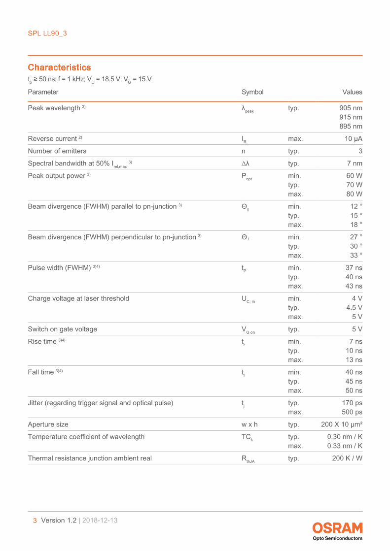
SPL LL90_3
1 Version 1.2 | 2018-12-13
Produktdatenblatt | Version 1.1 www.osram-os.com
Applications
SPL LL90_3
Radial Smart Laser Hybrid Pulsed Laser Diode with Integrated Driver Stage 905 nm, 70 W Peak Power
— Electronic Equipment
— Equipment Illumination (e.g. Curing, Endo-scope) — Highbay Industrial
— Industrial Automation (Machine Controls, Light Barriers, Vision Controls) — LIDAR, Pre-Crash, ACC
— Safety and Security, CCTV
Features: — Qualifications: The product qualification test plan is based on the guidelines of AEC-Q101-REV-C, Stress Test Qualification for Automotive Grade Discrete Semiconductors. — Laser wavelength 905 nm — Low cost, small size plastic package — Integrated FET and capacitors for pulse control — Strained InAIGaAs/GaAs QW-structures — High power large-optical-cavity laser structure — Nanostack laser technology including multiple epitaxially stacked emitters — High-speed operation (< 30 ns pulse width) — Low supply voltage (< 20 V)
Ordering Information
Type Peak output power Ordering Codetyp.tp ≥ 50 ns; f = 1 kHz; VC = 18.5 V; VG = 15 VPopt
SPL LL90_3 70 W Q65110A1009

SPL LL90_3
2 Version 1.2 | 2018-12-13
Maximum Ratingsshort time operation, TA = 25°C
Parameter Symbol Values
Operating Temperature Top min. max.
-40 °C100 °C
Storage Temperature Tstg min. max.
-40 °C100 °C
Junction temperature 1) Tj max. 105 °C
Peak output power Popt max. 80 W
Duty cycle dc max. 0.1 %
Gate voltage VG min. max.
-20 V20 V
Charge voltage VG = 15 V
VC max. 20 V
Reverse voltage 2) VR max. 12 V
Soldering temperature tmax = 10 s
TS max. 260 °C
SPL LL90_3
3 Version 1.2 | 2018-12-13
Characteristicstp ≥ 50 ns; f = 1 kHz; VC = 18.5 V; VG = 15 V
Parameter Symbol Values
Peak wavelength 3) λpeak typ. 905 nm915 nm895 nm
Reverse current 2) IR max. 10 µA
Number of emitters n typ. 3
Spectral bandwidth at 50% Irel,max 3) ∆λ typ. 7 nm
Peak output power 3) Popt min. typ. max.
60 W70 W80 W
Beam divergence (FWHM) parallel to pn-junction 3) Θ‖ min. typ. max.
12 °15 °18 °
Beam divergence (FWHM) perpendicular to pn-junction 3) Θ┴ min. typ. max.
27 °30 °33 °
Pulse width (FWHM) 3)4) tP min. typ. max.
37 ns40 ns43 ns
Charge voltage at laser threshold UC, th min. typ. max.
4 V4.5 V
5 V
Switch on gate voltage VG on typ. 5 V
Rise time 3)4) tr min. typ. max.
7 ns10 ns13 ns
Fall time 3)4) tf min. typ. max.
40 ns45 ns50 ns
Jitter (regarding trigger signal and optical pulse) tj typ. max.
170 ps500 ps
Aperture size w x h typ. 200 X 10 µm²
Temperature coefficient of wavelength TCλ typ. max.
0.30 nm / K0.33 nm / K
Thermal resistance junction ambient real RthJA typ. 200 K / W
SPL LL90_3
4 Version 1.2 | 2018-12-13
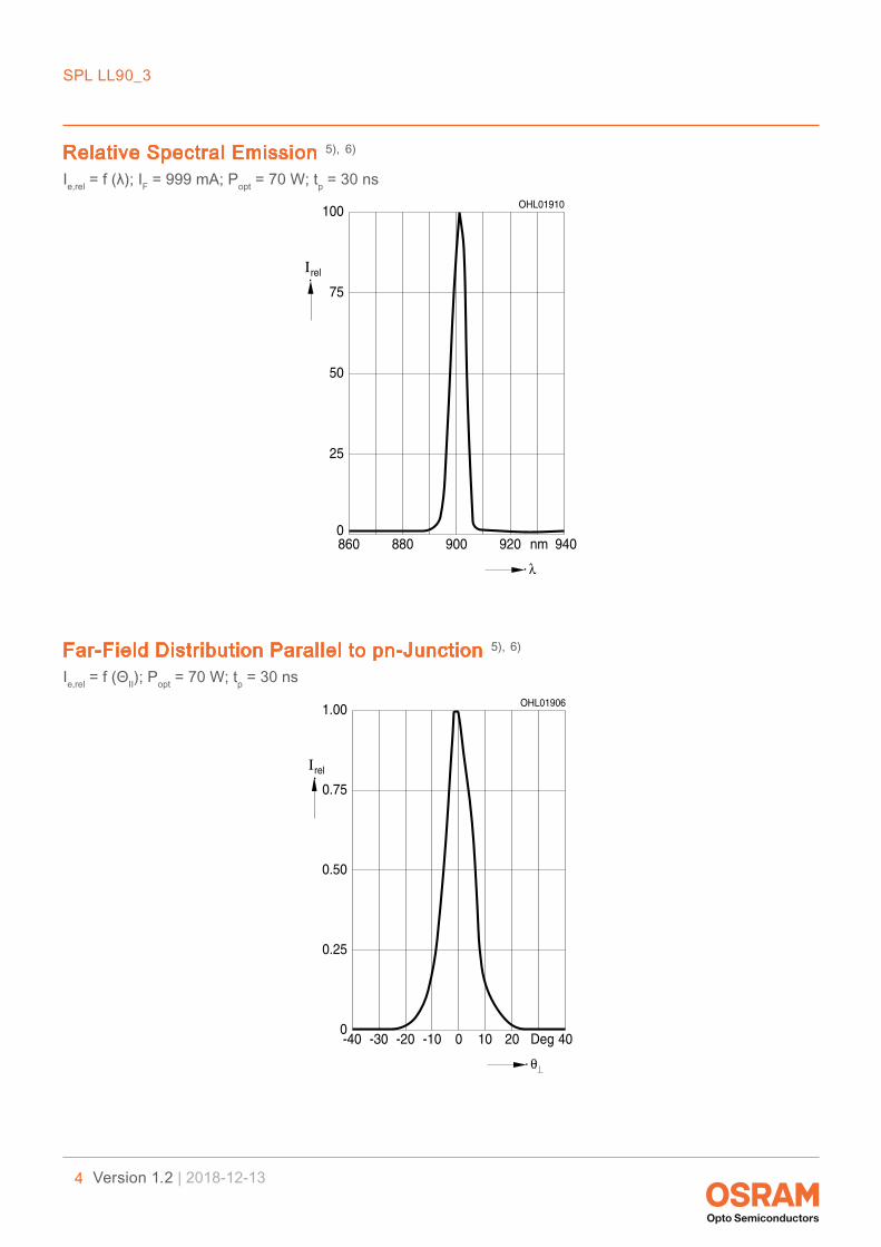
Relative Spectral Emission 5), 6)
Ie,rel = f (λ); IF = 999 mA; Popt = 70 W; tp = 30 ns
8600
OHL01910
relI
λ
880 900 920 nm 940
25
50
75
100
Far-Field Distribution Parallel to pn-Junction 5), 6)
Ie,rel = f (ΘII); Popt = 70 W; tp = 30 ns
-400
OHL01906
relI
θ
-30 -20 -10 0 10 20 Deg 40
0.25
0.50
0.75
1.00

SPL LL90_3
5 Version 1.2 | 2018-12-13
Far-Field Distribution Perpendicular to pn-Junction 5), 6)
Ie,rel = f (Θ⊥); Popt = 70 W; tp = 30 ns
-400
OHL01907
relI
θ
-30 -20 -10 0 10 20 Deg 40
0.25
0.50
0.75
1.00
Peak Output Power 5)
Popt = f (TA); tp = 30 ns
-400
T
Popt
OHL01905
A
40 kHz
10 kHz1 kHz
20 kHz30 kHz
10
20
30
40
50
60
70
80W
-20 0 20 40 60 80 ˚C 120
Optical Output Power 5), 6)
Popt = f (VC); tp = 30 ns; PRF = 1 kHz
00
V
Popt
OHL01908
C
5 10 15 20 25
10
20
30
40
50
60
70
80
90
V
W TA =-40 ˚C-20 ˚C
0 ˚C20 ˚C40 ˚C60 ˚C80 ˚C
100 ˚C

SPL LL90_3
6 Version 1.2 | 2018-12-13
Optical Output Power 5), 6)
Popt = f (VC); tp = 30 ns; PRF = 1 kHz
00
V
Popt
OHL01909
C
5 10 15 20 25
10
20
30
40
50
60
70
80
90
V
W
1 kHz
25 kHz
Max. Charge Voltage 5)
VC,max = f (TA); tp = 30 ns; VC ≤ 19 V; Tchip ≤ 105 °C
-400
T
VC max
OHL01904
A
40 kHz
10 kHz20 kHz30 kHz
-20 0 20 40 60 80 ˚C 120
2
4
6
8
10
12
14
16
18
20V
Dimensional Drawing 7)
GWOY7046
±0.2 (0.008)4.9 (0.193)
(12.
2 (0
.480
))
0.3
(0.0
12)+0
.4 (0
.016
)
25.2
(0.9
92)
24.2
(0.9
53)
1 2 3
0.5 (0.020)
1.8
(0.0
71)
1.2
(0.0
47)
2.4 (0.094)±0.2 (0.008)
±0.2 (0.008)1.35 (0.053)
(2.3
5 (0
.093
))
8.6
(0.3
39)±
0.4
(0.0
16)
Surfacenot flat
1.05 (0.041)±0.3 (0.012)
2
3
1C C
D
SG
Laser diode
TriggerG
CFET
GND
Laser Diode
spacing 2.54 (0.100)
0.6 (0.024)
0.4 (0.016)
-0.2
5 (0
.010
)
±0.1 (0.004)
0 (0.000)±0.1 (0.004)
0 (0.000)±0.1 (0.004)
0 (0.000)±0.1 (0.004)
0 (0.000)±0.1 (0.004)
±0.2 (0.008)2.5 (0.098)±0.2 (0.008)5 (0.197)
R0.3 (0.012)
R0.25 (0.010)
V
V
0.5 (0.020)±0.1 (0.004)
spacing 1.27 (0.050)
0˚ ±5˚ref. to leadframe centerline

SPL LL90_3
7 Version 1.2 | 2018-12-13
Approximate Weight: 430.0 mg
SPL LL90_3
8 Version 1.2 | 2018-12-13
NotesDepending on the mode of operation, these devices emit highly concentrated visible and non visible light light which can be hazardous to the human eye. Products which incorporate these devices have to follow the safety precautions given in IEC 60825-1.
Subcomponents of this device contain, in addition to other substances, metal filled materials including silver. Metal filled materials can be affected by environments that contain traces of aggressive substances. There-fore, we recommend that customers minimize device exposure to aggressive substances during storage, production, and use. Devices that showed visible discoloration when tested using the described tests above did show no performance deviations within failure limits during the stated test duration. Respective failure limits are described in the IEC60810.
For further application related informations please visit www.osram-os.com/appnotes
SPL LL90_3
9 Version 1.2 | 2018-12-13
Disclaimer
Attention please!The information describes the type of component and shall not be considered as assured characteristics. Terms of delivery and rights to change design reserved. Due to technical requirements components may contain dangerous substances.For information on the types in question please contact our Sales Organization.If printed or downloaded, please find the latest version on the OSRAM OS webside.
PackingPlease use the recycling operators known to you. We can also help you – get in touch with your nearest sales office.By agreement we will take packing material back, if it is sorted. You must bear the costs of transport. For packing material that is returned to us unsorted or which we are not obliged to accept, we shall have to invoice you for any costs incurred.
Product safety devices/applications or medical devices/applicationsOSRAM OS components are not developed, constructed or tested for the application as safety relevant component or for the application in medical devices. In case Buyer – or Customer supplied by Buyer– considers using OSRAM OS components in product safety devices/applications or medical devices/applications, Buyer and/or Customer has to inform the local sales partner of OSRAM OS immediately and OSRAM OS and Buyer and /or Customer will analyze and coordi-nate the customer-specific request between OSRAM OS and Buyer and/or Customer.
SPL LL90_3
10 Version 1.2 | 2018-12-13
Glossary1) Junction temperature: Limited due to plastic package, not due to laser chip.2) Reverse Operation: Reverse Operation of 10 hours is permissible in total. Continuous reverse opera-
tion is not allowed.3) Driver information: The laser is driven by the MOSFET driver Elantec EL7104C.4) Switching speed: Switching speed at gate depends on current and speed, charging the gate capaci-
tance (typ. 300 pF) of the internal transistor. Reduced pulse widths, rise and fall times occur at trigger pulse widths < 50 ns. This also reduces the optical peak power.
5) Typical Values: Due to the special conditions of the manufacturing processes of semiconductor devic-es, the typical data or calculated correlations of technical parameters can only reflect statistical figures. These do not necessarily correspond to the actual parameters of each single product, which could dif-fer from the typical data and calculated correlations or the typical characteristic line. If requested, e.g. because of technical improvements, these typ. data will be changed without any further notice.
6) Testing temperature: TA = 25°C7) Tolerance of Measure: Unless otherwise noted in drawing, tolerances are specified with ±0.1 and
dimensions are specified in mm.

SPL LL90_3
11 Version 1.2 | 2018-12-13
Revision HistoryVersion Date Change
1.2 2018-12-13 Additional Information

SPL LL90_3
12 Version 1.2 | 2018-12-13
Published by OSRAM Opto Semiconductors GmbH Leibnizstraße 4, D-93055 Regensburg www.osram-os.com © All Rights Reserved.