Embed Size (px)
Citation preview
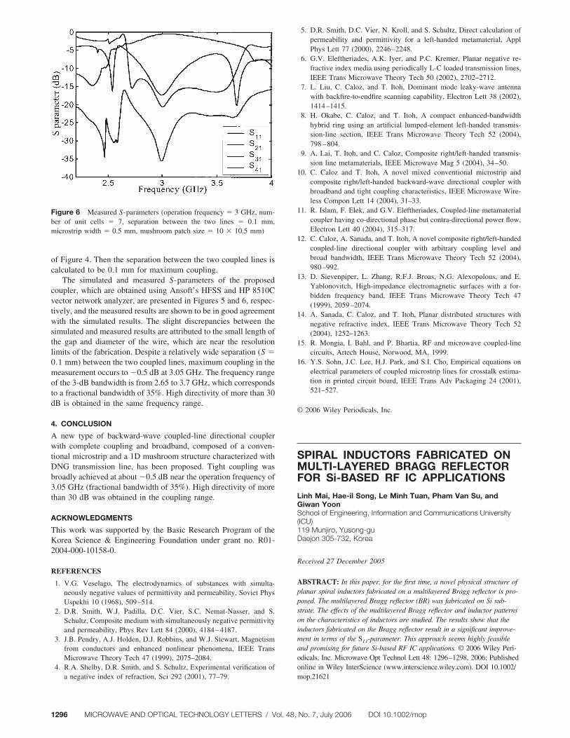
of Figure 4. Then the separation between the two coupled lines iscalculated to be 0.1 mm for maximum coupling.
The simulated and measured S-parameters of the proposedcoupler, which are obtained using Ansoft’s HFSS and HP 8510Cvector network analyzer, are presented in Figures 5 and 6, respec-tively, and the measured results are shown to be in good agreementwith the simulated results. The slight discrepancies between thesimulated and measured results are attributed to the small length ofthe gap and diameter of the wire, which are near the resolutionlimits of the fabrication. Despite a relatively wide separation (S �0.1 mm) between the two coupled lines, maximum coupling in themeasurement occurs to �0.5 dB at 3.05 GHz. The frequency rangeof the 3-dB bandwidth is from 2.65 to 3.7 GHz, which correspondsto a fractional bandwidth of 35%. High directivity of more than 30dB is obtained in the same frequency range.
4. CONCLUSION
A new type of backward-wave coupled-line directional couplerwith complete coupling and broadband, composed of a conven-tional microstrip and a 1D mushroom structure characterized withDNG transmission line, has been proposed. Tight coupling wasbroadly achieved at about �0.5 dB near the operation frequency of3.05 GHz (fractional bandwidth of 35%). High directivity of morethan 30 dB was obtained in the coupling range.
ACKNOWLEDGMENTS
This work was supported by the Basic Research Program of theKorea Science & Engineering Foundation under grant no. R01-2004-000-10158-0.
REFERENCES
1. V.G. Veselago, The electrodynamics of substances with simulta-neously negative values of permittivity and permeability, Soviet PhysUspekhi 10 (1968), 509–514.
2. D.R. Smith, W.J. Padilla, D.C. Vier, S.C. Nemat-Nasser, and S.Schultz, Composite medium with simultaneously negative permittivityand permeability, Phys Rev Lett 84 (2000), 4184–4187.
3. J.B. Pendry, A.J. Holden, D.J. Robbins, and W.J. Stewart, Magnetismfrom conductors and enhanced nonlinear phenomena, IEEE TransMicrowave Theory Tech 47 (1999), 2075–2084.
4. R.A. Shelby, D.R. Smith, and S. Schultz, Experimental verification ofa negative index of refraction, Sci 292 (2001), 77–79.
5. D.R. Smith, D.C. Vier, N. Kroll, and S. Schultz, Direct calculation ofpermeability and permittivity for a left-handed metamaterial, ApplPhys Lett 77 (2000), 2246–2248.
6. G.V. Eleftheriades, A.K. Iyer, and P.C. Kremer, Planar negative re-fractive index media using periodically L-C loaded transmission lines,IEEE Trans Microwave Theory Tech 50 (2002), 2702–2712.
7. L. Liu, C. Caloz, and T. Itoh, Dominant mode leaky-wave antennawith backfire-to-endfire scanning capability, Electron Lett 38 (2002),1414–1415.
8. H. Okabe, C. Caloz, and T. Itoh, A compact enhanced-bandwidthhybrid ring using an artificial lumped-element left-handed transmis-sion-line section, IEEE Trans Microwave Theory Tech 52 (2004),798–804.
9. A. Lai, T. Itoh, and C. Caloz, Composite right/left-handed transmis-sion line metamaterials, IEEE Microwave Mag 5 (2004), 34–50.
10. C. Caloz and T. Itoh, A novel mixed conventional microstrip andcomposite right/left-handed backward-wave directional coupler withbroadband and tight coupling characteristics, IEEE Microwave Wire-less Compon Lett 14 (2004), 31–33.
11. R. Islam, F. Elek, and G.V. Eleftheriades, Coupled-line metamaterialcoupler having co-directional phase but contra-directional power flow,Electron Lett 40 (2004), 315–317.
12. C. Caloz, A. Sanada, and T. Itoh, A novel composite right/left-handedcoupled-line directional coupler with arbitrary coupling level andbroad bandwidth, IEEE Trans Microwave Theory Tech 52 (2004),980–992.
13. D. Sievenpiper, L. Zhang, R.F.J. Broas, N.G. Alexopolous, and E.Yablonovitch, High-impedance electromagnetic surfaces with a for-bidden frequency band, IEEE Trans Microwave Theory Tech 47(1999), 2059–2074.
14. A. Sanada, C. Caloz, and T. Itoh, Planar distributed structures withnegative refractive index, IEEE Trans Microwave Theory Tech 52(2004), 1252–1263.
15. R. Mongia, I. Bahl, and P. Bhartia, RF and microwave coupled-linecircuits, Artech House, Norwood, MA, 1999.
16. Y.S. Sohn, J.C. Lee, H.J. Park, and S.I. Cho, Empirical equations onelectrical parameters of coupled microstrip lines for crosstalk estima-tion in printed circuit board, IEEE Trans Adv Packaging 24 (2001),521–527.
© 2006 Wiley Periodicals, Inc.
SPIRAL INDUCTORS FABRICATED ONMULTI-LAYERED BRAGG REFLECTORFOR Si-BASED RF IC APPLICATIONS
Linh Mai, Hae-il Song, Le Minh Tuan, Pham Van Su, andGiwan YoonSchool of Engineering, Information and Communications University(ICU)119 Munjiro, Yusong-guDaejon 305-732, Korea
Received 27 December 2005
ABSTRACT: In this paper, for the first time, a novel physical structure ofplanar spiral inductors fabricated on a multilayered Bragg reflector is pro-posed. The multilayered Bragg reflector (BR) was fabricated on Si sub-strate. The effects of the multilayered Bragg reflector and inductor patternson the characteristics of inductors are studied. The results show that theinductors fabricated on the Bragg reflector result in a significant improve-ment in terms of the S11-parameter. This approach seems highly feasibleand promising for future Si-based RF IC applications. © 2006 Wiley Peri-odicals, Inc. Microwave Opt Technol Lett 48: 1296–1298, 2006; Publishedonline in Wiley InterScience (www.interscience.wiley.com). DOI 10.1002/mop.21621
Figure 6 Measured S-parameters (operation frequency � 3 GHz, num-ber of unit cells � 7, separation between the two lines � 0.1 mm,microstrip width � 0.5 mm, mushroom patch size � 10 � 10.5 mm)
1296 MICROWAVE AND OPTICAL TECHNOLOGY LETTERS / Vol. 48, No. 7, July 2006 DOI 10.1002/mop

Key words: spiral inductor; inductor layout; Bragg reflector; returnloss (S11); silicon substrate
1. INTRODUCTION
The design of high-quality passive elements in the silicon-basedradio-frequency integrated circuits (RFICs) area has been one ofthe key issues in wireless communication systems. Performancesof several basic RF blocks such as low-noise amplifiers, mixers,and voltage-controlled oscillators depend mainly on the quality ofthe passive elements. Overall, an on-chip spiral inductor can be akey component among passive elements. In general, the RF micro-inductors have been fabricated on the planar substrates such assilicon or glass [1–3]. Unfortunately, the losses occurring mainlydue to conductive substrates and thin metal strips have been acritical issue, making it hard to improve the performance of theplanar inductors. In order to resolve this issue, many techniques todecrease the substrate loss and ohmic loss have been proposed. Forinstance, Taub et al. proposed high-resistive silicon or silicon-on-insulator as the substrate [4], while Larson [5] used thick dielectriclayers to reduce the substrate loss and higher-conductivity metalsuch as gold to lower the resistance loss of the spiral inductors.Another method to reduce substrate loss is the removal of theconductive substrate [6, 7]. By those reported techniques, the highQ-value of the on-chip inductors could have been achieved at thecost of process complexity and incompatibility, and the reductionof mechanical strength, which cause some physical limitations fordevice fabrication and commercialization.
In this paper, we propose a feasibility study of a new RF spiralinductor structure incorporating the multilayered Bragg reflectorbetween the spiral inductor and Si substrate. As a result, theinductor performance can be improved mainly due to the reductionof the Si substrate loss.
2. EXPERIMENT
Three sets of different spiral inductors (I1, I2, and I3) are simul-taneously prepared on three different silicon-based substrates Si,SiO2/Si, and BR/Si, respectively. Figure 1 illustrates the differentinductor structures implemented in this work: (a) inductor on Sisubstrate, (b) inductor on SiO2/Si substrate, and (c) inductor on aseven-layered Bragg reflector/Si substrate. The first spiral inductortype (I1) was fabricated directly on Si wafer in order to use it as areference sample. The second type of spiral inductor (I2) wasfabricated similarly to the first one, but the spiral inductors wereseparated from the Si substrate by 0.6-�m-thick thermal silicondioxide (SiO2). As proposed in this work, the third inductorstructure (I3) was fabricated on the multilayered Bragg reflector/silicon substrate (BR/Si). The seven-layered Bragg reflector con-sisted of SiO2 and tungsten (W) films and was prepared by alter-nate deposition of W and SiO2 layers in an RF magnetronsputtering system. The 0.6-�m-thick W films were deposited un-der Ar gas pressure of 15 mTorr with DC power of 150 Watts, andthe 0.6-�m-thick SiO2 films were deposited under Ar gas pressureof 4 mTorr with RF power of 300 Watts. Each spiral inductor wasfabricated using 0.2-�m-thick aluminum (Al) with 1.2-�m-thickzinc oxide (ZnO). The 0.2-�m-thick Al thin films (lower metalstrips) were simultaneously deposited on all three substrates under20 mTorr Ar gas pressure and with 150-Watts DC power. Then,the 1.2-�m-thick ZnO film with via-patterning was depositedunder 10 mTorr of Ar/O2 mixed-gases, and with RF power of 300Watts. The deposition and patterning of the upper Al strips (0.2�m) on top of the ZnO film completed the spiral-inductor fabri-cation. All the upper metal strips were connected to the lower onesthrough via-holes. Finally, the three spiral inductor types (I1, I2,
and I3), corresponding to the substrates of Si, SiO2/Si, and BR/Si,respectively, were fabricated. All the spiral-inductor structureswere measured to extract the de-embedded S-parameters usingboth a probe station and a network analyzer (Hewlet Packard/HP8722D).
3. RESULTS AND DISCUSSION
In this study, three different spiral-inductor layouts were designedand each spiral layout was fabricated on three different substratestructures, as described in Figure 1. The measured S-parametervalues of the three inductor patterns were plotted as a function offrequency, as shown in Figure 2. The three spiral inductor layoutshave 2.5 turns and numbers of sides are 12, 14, and 16, respec-tively. Figures 2(a), 2(b), and 2(c) compare the return-loss char-acteristics of the three spiral inductor structures (namely, L1, L2,and L3) with the same inductor layout, each fabricated on the Si,SiO2/Si, and BR/Si substrates, respectively. The comparison of theS11 values clearly shows the relative effect of the substrate struc-ture used. Regardless of the spiral-layout types, the return-lossvalues have the same increasing trend in sequence from the induc-tors L1 (Si substrate), L2 (SiO2/Si substrate), and L3 (BR/Sisubstrate). For three physical inductor structures, the S11 charac-teristic of the inductor L2 is better than that of L1 due to thedielectric layer SiO2 being incorporated between the spiral induc-
Figure 1 Cross-sectional 3D structures of the on-chip inductors: (a)inductor on Si substrate; (b) inductor on SiO2/Si substrate; (c) inductor onseven-layered BR/Si substrate. [Color figure can be viewed in the onlineissue, which is available at www.interscience.wiley.com]
DOI 10.1002/mop MICROWAVE AND OPTICAL TECHNOLOGY LETTERS / Vol. 48, No. 7, July 2006 1297
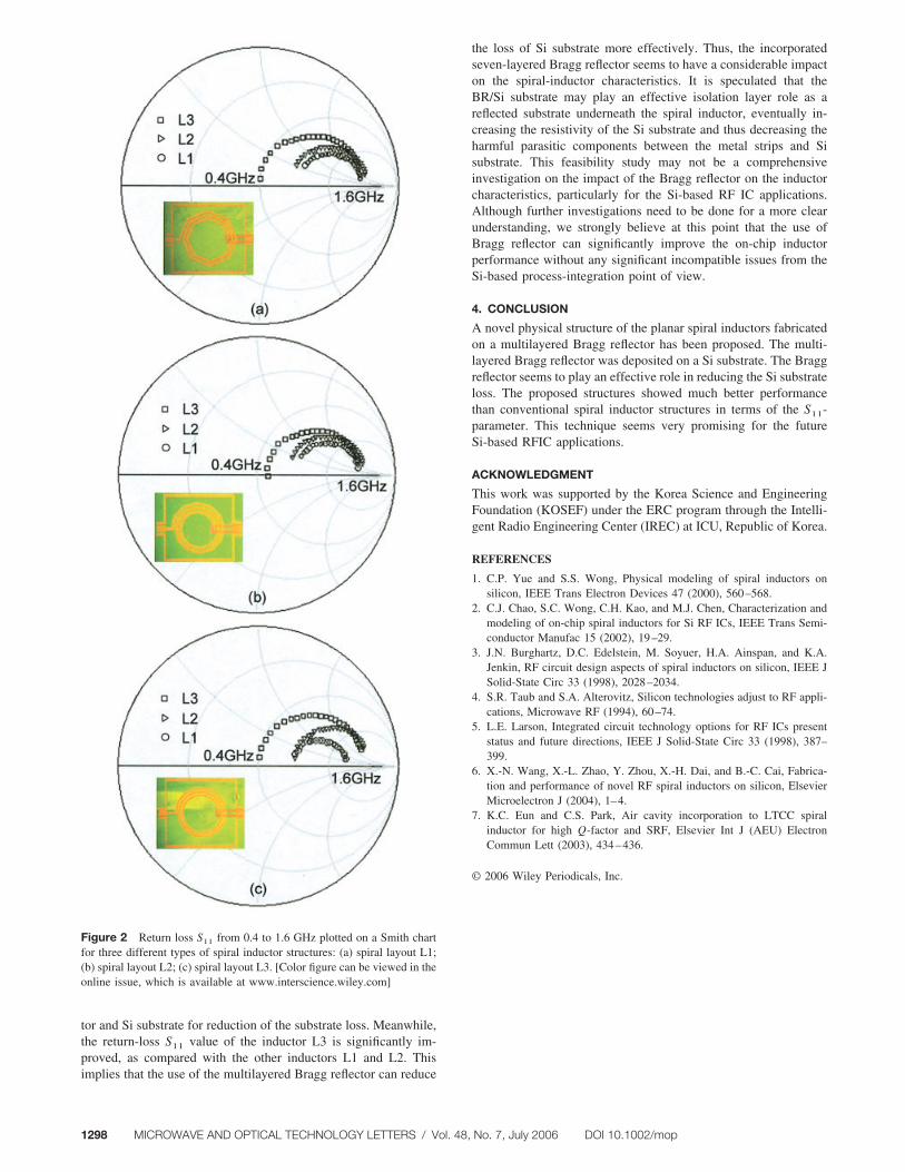
tor and Si substrate for reduction of the substrate loss. Meanwhile,the return-loss S11 value of the inductor L3 is significantly im-proved, as compared with the other inductors L1 and L2. Thisimplies that the use of the multilayered Bragg reflector can reduce
the loss of Si substrate more effectively. Thus, the incorporatedseven-layered Bragg reflector seems to have a considerable impacton the spiral-inductor characteristics. It is speculated that theBR/Si substrate may play an effective isolation layer role as areflected substrate underneath the spiral inductor, eventually in-creasing the resistivity of the Si substrate and thus decreasing theharmful parasitic components between the metal strips and Sisubstrate. This feasibility study may not be a comprehensiveinvestigation on the impact of the Bragg reflector on the inductorcharacteristics, particularly for the Si-based RF IC applications.Although further investigations need to be done for a more clearunderstanding, we strongly believe at this point that the use ofBragg reflector can significantly improve the on-chip inductorperformance without any significant incompatible issues from theSi-based process-integration point of view.
4. CONCLUSION
A novel physical structure of the planar spiral inductors fabricatedon a multilayered Bragg reflector has been proposed. The multi-layered Bragg reflector was deposited on a Si substrate. The Braggreflector seems to play an effective role in reducing the Si substrateloss. The proposed structures showed much better performancethan conventional spiral inductor structures in terms of the S11-parameter. This technique seems very promising for the futureSi-based RFIC applications.
ACKNOWLEDGMENT
This work was supported by the Korea Science and EngineeringFoundation (KOSEF) under the ERC program through the Intelli-gent Radio Engineering Center (IREC) at ICU, Republic of Korea.
REFERENCES
1. C.P. Yue and S.S. Wong, Physical modeling of spiral inductors onsilicon, IEEE Trans Electron Devices 47 (2000), 560–568.
2. C.J. Chao, S.C. Wong, C.H. Kao, and M.J. Chen, Characterization andmodeling of on-chip spiral inductors for Si RF ICs, IEEE Trans Semi-conductor Manufac 15 (2002), 19–29.
3. J.N. Burghartz, D.C. Edelstein, M. Soyuer, H.A. Ainspan, and K.A.Jenkin, RF circuit design aspects of spiral inductors on silicon, IEEE JSolid-State Circ 33 (1998), 2028–2034.
4. S.R. Taub and S.A. Alterovitz, Silicon technologies adjust to RF appli-cations, Microwave RF (1994), 60–74.
5. L.E. Larson, Integrated circuit technology options for RF ICs presentstatus and future directions, IEEE J Solid-State Circ 33 (1998), 387–399.
6. X.-N. Wang, X.-L. Zhao, Y. Zhou, X.-H. Dai, and B.-C. Cai, Fabrica-tion and performance of novel RF spiral inductors on silicon, ElsevierMicroelectron J (2004), 1–4.
7. K.C. Eun and C.S. Park, Air cavity incorporation to LTCC spiralinductor for high Q-factor and SRF, Elsevier Int J (AEU) ElectronCommun Lett (2003), 434–436.
© 2006 Wiley Periodicals, Inc.
Figure 2 Return loss S11 from 0.4 to 1.6 GHz plotted on a Smith chartfor three different types of spiral inductor structures: (a) spiral layout L1;(b) spiral layout L2; (c) spiral layout L3. [Color figure can be viewed in theonline issue, which is available at www.interscience.wiley.com]
1298 MICROWAVE AND OPTICAL TECHNOLOGY LETTERS / Vol. 48, No. 7, July 2006 DOI 10.1002/mop