Embed Size (px)
Citation preview

Spin Transfer Torque Devices as an Embedded
non-volatile Memory
Sayeef Salahuddin
Electrical Engineering and Computer Sciences, UC Berkeley
Research group: LEED (Laboratory for Emerging and Exploratory Devices)http://leed.eecs.berkeley.edu

LEED@Berkeley E3S-Seminar 2
Memory Technologies and MRAM
source: http://www.ts.avnet.com/
0.5 V, non-volatile, high endurance, write
speed ~ few ns
Plausible non-volatile
solution in this space
Kubota et. al., JJAP, 44, 40, 1237,2005
Free Magnet
Tunnel oxide
Fixed Magnet
I
64 MB DRAM like STT MRAMAvailable from Everspin

LEED@Berkeley E3S-Seminar 3
A recent announcement

LEED@Berkeley E3S-Seminar 4
Embedded Non-Volatile Memory
Data Bus

LEED@Berkeley E3S-Seminar 5
Embedded Non-Volatile Memory
Data Bus
Memory layer
• Significant reduction in energy mobile computing• Non volatility is a prime requirement for machine learning applications

LEED@Berkeley E3S-Seminar 6
Competition
• Slightly slower than SRAM• Smaller than SRAM• Same endurance

LEED@Berkeley E3S-Seminar 7
MRAM scaling TrendsI/D
Lateral Dimension
Fe
MgO
3-4X
3-4X
?
Field driven
MRAM
SpinMRAM
SpinMRAM
With PMA
Scaling of write current for a given memory retention time
Memory retention time ~ exp(D)

LEED@Berkeley E3S-Seminar 8
The Traditional MRAM
Tunnel Oxide
Pinned Magnet
Soft Magnet
Flowing electrons are predominantly composed of the type of spins based on the magnetization direction of the magnet that injects them.
• Non-volatility > 10 years (typical)• Unlimited Endurance
LEED@Berkeley E3S-Seminar 9
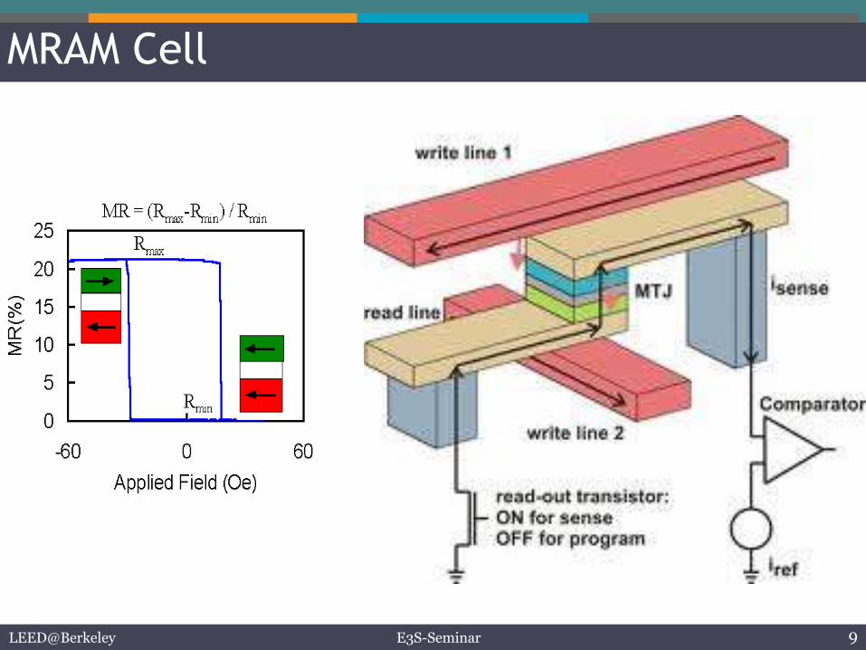
MRAM Cell

LEED@Berkeley E3S-Seminar 10
But..MRAM does not scale
Smith et al, Future Fab International, Issue 23
𝐼 ∝ 1/𝐿
LEED@Berkeley E3S-Seminar 11
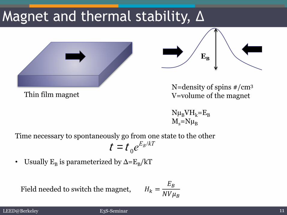
Magnet and thermal stability, Δ
EB
t = t 0eEB /kT
• Usually EB is parameterized by Δ=EB/kT
Time necessary to spontaneously go from one state to the other
Thin film magnet
NµBVHk=EB
Ms=NµB
N=density of spins #/cm3
V=volume of the magnet
Field needed to switch the magnet, 𝐻𝑘 =𝐸𝐵
𝑁𝑉𝜇𝐵
LEED@Berkeley E3S-Seminar 12
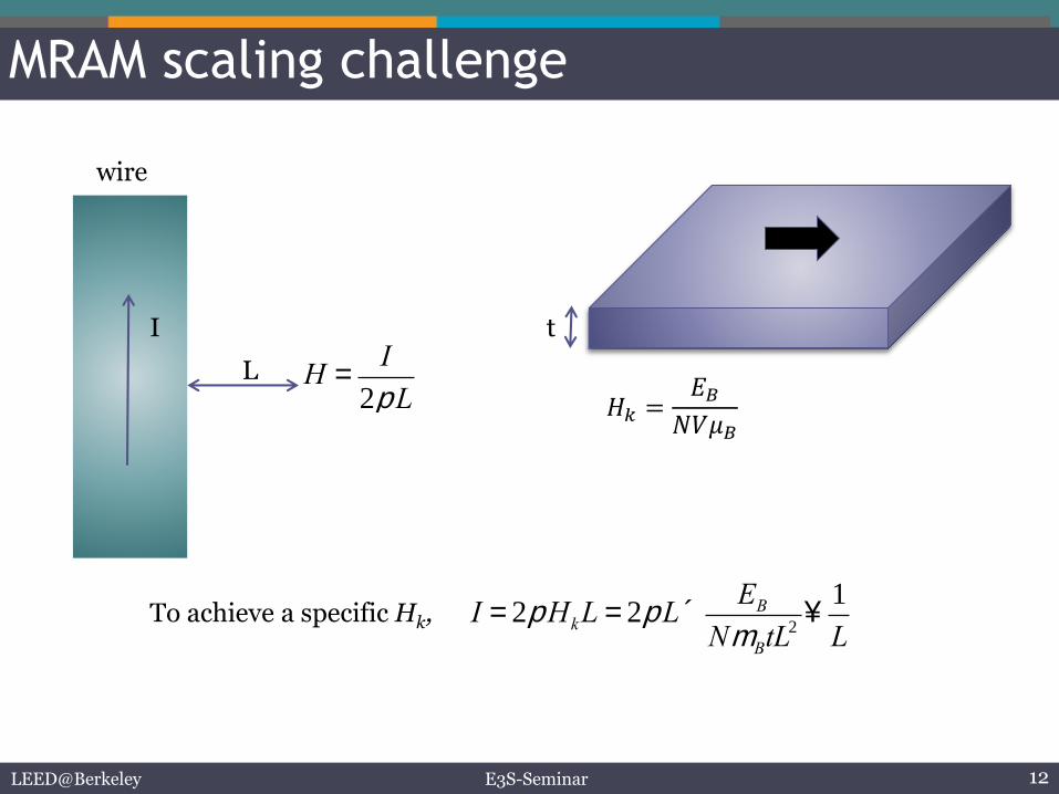
MRAM scaling challenge
wire
L
I
H =I
2pL
t
I = 2pHkL = 2pL´EB
Nm BtL2
¥1
LTo achieve a specific Hk,
𝐻𝑘 =𝐸𝐵
𝑁𝑉𝜇𝐵

LEED@Berkeley E3S-Seminar 13
MRAM scaling TrendsI/D
Lateral Dimension
Fe
MgO
3-4X
3-4X
?
Field driven
MRAM
SpinMRAM
SpinMRAM
With PMA
Scaling of write current for a given memory retention time
Memory retention time ~ exp(D)

LEED@Berkeley E3S-Seminar 14
Spin Transfer Torque Devices
Bottom Electrode
CoFe (2.5)
Ru (0.85)
Insulator
Top Electrode
CoFeB (3)
CoFeB (3)
MgO (0.85)
Pinned layer
Soft layer
Oxide 0
0R
Current
Pinned layer Soft layer
Kubota et. al., JJAP, 44, 40, 1237,2005
Slonczewski: JMMM 1996, 2002,2007PRB 1989, 2005First experiment:Phys. Rev. Lett. 84, 3149 (2000)

Bottom Electrode
CoFe (2.5)
Ru (0.85)
Insulator
Top Electrode
CoFeB (3)
CoFeB (3)
MgO (0.85)
Co
FeB
Mg
OC
oF
eB
Spin accumulation due to non-equilibrium spin transport
Spin current absorbed inside ‘soft magnet’
Simple Physics of Spin Torque
LEED@Berkeley E3S-Seminar 15

LEED@Berkeley E3S-Seminar 16
Physics of STT Devices: Thin film magnets
Field lines
Field lines
Magnetostatics legislates that a thin film magnet be polarized in-plane

LEED@Berkeley E3S-Seminar 17
Simple Physics of Spin Torque Transfer
t
Spin angular momentum has to be conserved.
If we are flipping the magnet from right to left, one must provide a (NV) amount of left polarized spins
Required number of electrons, n = NV
h
η is the spin polarization efficiency
Current needed to switch the magnet: I =en
t= eN
h
1
t
æ
èç
ö
ø÷(t)L2
𝑉 = 𝐿2𝑡
L
𝐼 = 𝑒𝑛/𝜏
Switching current scales with footprint area and thickness

LEED@Berkeley E3S-Seminar 18
Switching of the magnet by current
t
I
γ=gyromagnetic ratio=gµB/ħ=2µB/ħ
Heff=Hanisotrpy+2πMs+Hexternal
Characteristic time, τ, to switch a magnet:
𝑑 𝑚
𝑑𝑡= −𝛾 𝑚 × 𝐻𝑒𝑓𝑓
;α=damping

LEED@Berkeley E3S-Seminar 19
Scaling of Spin RAM
Thermal stability : Anisotropy field:
In-plane MRAM scales
𝐻𝑎 ≡ 𝐻𝑘
𝐼 =2𝑒
ℏ𝛼
𝑀𝑠
𝜂𝐻𝑎 + 2𝜋𝑀𝑠 𝑡 𝐿𝑊
Δ = 𝑀𝑠𝐻𝑘 𝑡 𝐿𝑊 𝐻𝑘 ∝ 𝑡1
𝑊−1
𝐿
𝐼
Δ≈ 𝑀𝑠
𝛼
𝜂
𝑊𝐿
𝐿 −𝑊 𝑡1 +
2𝜋𝑀𝑠
𝐻𝑘~𝜆
If L and W are both scaled by λ

LEED@Berkeley E3S-Seminar 20
MRAM scaling TrendsI/D
Lateral Dimension
Fe
MgO
3-4X
3-4X
?
Field driven
MRAM
SpinMRAM
SpinMRAM
With PMA
Scaling of write current for a given memory retention time
Memory retention time ~ exp(D)

LEED@Berkeley E3S-Seminar 21
Issues with in-plane MRAM
Hk~100-200 OeMs ~600-1200 Oe
• Difficult to keep reducing dimensions keeping intact the aspect ratio
• The area is always much larger compared to what is possible with minimum feature size.
𝐼
Δ≈ 𝑀𝑠
𝛼
𝜂
𝑊𝐿
𝐿 −𝑊 𝑡1 +
2𝜋𝑀𝑠
𝐻𝑘
1 +2𝜋𝑀𝑠
𝐻𝑘~20-50

LEED@Berkeley E3S-Seminar 22
Perpendicular STT MRAM
• In a Fe-MgO interface Fe-O bonds can provide the required crystalline anisotropy
• There is no reason to have shape anisotropy any more, the magnets can be circular
𝐼𝑓 𝑎 𝑐𝑟𝑦𝑠𝑡𝑎𝑙𝑙𝑖𝑛𝑒 𝑎𝑛𝑖𝑠𝑜𝑡𝑟𝑜𝑝𝑦 𝑐𝑎𝑛 𝑏𝑒 𝑐𝑟𝑒𝑎𝑡𝑒𝑑
Objective is to reduce: 1 +2𝜋𝑀𝑠
𝐻𝑘
𝐻𝑛𝑒𝑡 = 2𝜋M𝑠 −𝐻𝑃𝑀𝐴~0
the switching current can be 10X lower

LEED@Berkeley E3S-Seminar 23
Current drops but scaling goes away
M Gajek et. al, APL, 100, 132408 (2012)
29µA
𝐼 =2𝑒
ℏ𝛼
𝑀𝑠
𝜂𝐻𝑎 + 2𝜋𝑀𝑠 𝑡 𝐿𝑊 𝑛𝑜𝑤 𝑏𝑒𝑐𝑜𝑚𝑒𝑠
𝐼 =2𝑒
ℏ𝛼
𝑀𝑠
𝜂2𝜋𝑀𝑠 − 𝐻𝑃𝑀𝐴 𝑡 𝐿𝑊
Δ = 𝑀𝑠 2𝜋𝑀𝑠 − 𝐻𝑃𝑀𝐴 𝑡 𝐿𝑊
𝐼
Δ≈𝛼
𝜂 Scaling dependence is gone

LEED@Berkeley E3S-Seminar 24
Scaling Challenges
• To decrease current with scaling- decrease a
-increase h
• To keep the memory -increase 2𝜋𝑀𝑠 −𝐻𝑃𝑀𝐴
𝐼
Δ≈𝛼
𝜂Δ = 𝑀𝑠 2𝜋𝑀𝑠 − 𝐻𝑃𝑀𝐴 𝑡 𝐿𝑊

LEED@Berkeley E3S-Seminar 25
MRAM scaling TrendsI/D
Lateral Dimension
Fe
MgO
3-4X
3-4X
?
Field driven
MRAM
SpinMRAM
SpinMRAM
With PMA
Scaling of write current for a given memory retention time
Memory retention time ~ exp(D)

LEED@Berkeley E3S-Seminar 26
Competition
• Slightly slower than SRAM• Much smaller than SRAM• Same endurance
LEED@Berkeley E3S-Seminar 27
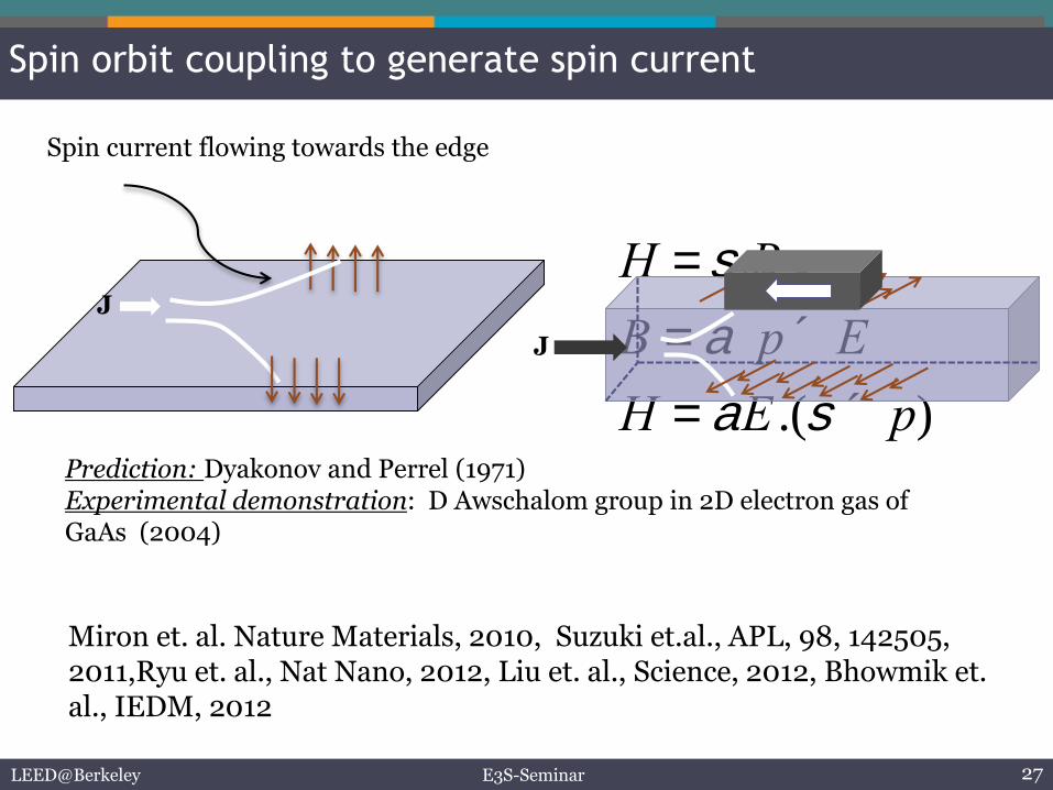
Spin orbit coupling to generate spin current
H = s.B
B = a p ´ E
H = aE .(s ´ p)Prediction: Dyakonov and Perrel (1971)Experimental demonstration: D Awschalom group in 2D electron gas of GaAs (2004)
J
J
Spin current flowing towards the edge
Miron et. al. Nature Materials, 2010, Suzuki et.al., APL, 98, 142505, 2011,Ryu et. al., Nat Nano, 2012, Liu et. al., Science, 2012, Bhowmik et. al., IEDM, 2012

LEED@Berkeley E3S-Seminar 28
Spin orbit generated spin current
Bhowmik, You and Salahuddin, Nature Nanotechnology,9,59 (2014)

LEED@Berkeley E3S-Seminar 29
Potential reduction in WRITE current
I
I
Spin Orbit Torque Device Spin Transfer Torque Device
I∝Width of the magnet x thickness of the wire
I∝Width of the magnet x length of
the magnet
So a potential reduction of (L/t) is possible

LEED@Berkeley E3S-Seminar 30
Potential Reduction in Current
l~2nm;
0 2 4 6 8 100.2
0.4
0.6
0.8
1
1.2
thickness in nm
I SO
/IS
TT
L=10 nm
L=15 nm
3-4X decrease in current is possible
ISO
ISTT=t
L
h
qso1+
cosech(t / l)
tanh(t / 2l)
é
ëê
ù
ûú
h
qso~ 1

LEED@Berkeley E3S-Seminar 31
Thickness dependence of SOT
• GFC is a Bulk PMA material
• Thermal stability can be retained by increasing thickness, unlike interfacial PMA, when the areal footprint is scaled can be very important for ultra scaled memory technologies
• Combined with lower current for SOT this could help resolve the scaling issue
But can we switch a large thickness GFC with SOT?
LEED@Berkeley E3S-Seminar 32
Scaling Trends Summary
10 15 20 25 3025
50
75
100Gd
21(Fe
90Co
10)79
Δt (nm)
10 15 20 25 300
2
4
6Gd
21(Fe
90Co
10)79
jHM
c (
10
7 A
/cm
2)
t (nm)
BIP
= 100 mT

LEED@Berkeley E3S-Seminar 33
Figure of Merit of SOT Switching
10 15 20 25 300
1
2
3
4
5
6
Gd21
(Fe90
Co10
)79
jHM
c/Δ
(1
05 A
/cm
2)
t (nm)
Fukami [1] Mihajlovic [2] Lee [3] Roschewsky0.0
0.1
0.2
0.3
0.4
0.5
j c/Δ (
10
7 A
/cm
2)
[1] S. Fukami, et al., Nat. Nanotech.,11, 7, 621–625, 2016
[2] G. Mihajlović, et al., Appl. Phys. Lett.,109, 19, 192404, 2016
[3] O. J. Lee, et al., Phys. Rev. B, 89, 2, 24418, 2014
Very high switching efficiency in ferrimagnetic GFC
(Rochewsky. C-H, Lambert et al, PRB, 2017)

LEED@Berkeley E3S-Seminar 34
Spin Orbit Torque in Ferrimagnetic Gdx(Fe90Co10)1-x
16 18 20 22 24 26 28 300.0
0.2
0.4
0.6
0.8
1.0
m (
no
rma
lize
d)
composition x (%)
Compensation:
x = 23.4
m(Gd)=7.2 B/atom
m(FeCo)=2.2 B/atom
Gdx(Fe90Co10)1-x
Radu et al., Nature 2011.
Gorchon et al, arxiv:1702.08492Yang et al. arxiv: 1609.06392 Wilson et al. arxiv: 1609.05155
J Bokor group

LEED@Berkeley E3S-Seminar 35
Array Issues due to low MR: Competition
Kubota et. al., JJAP, 44, 40, 1237,2005
BL
WL

LEED@Berkeley E3S-Seminar 36
Array Issues: Competition
BL1 BL2 BL3
WL1
WL2
WL3ION
IOFF
IOFF
Total current flowing in BL1= ION+n*IOFF; n is number of bits in the BL
So, if ION/IOFF~2, one cannot have more than 3 elements without a transistor
Due to the need of a transistor, currently STTRAM cannot be integrated in 3D

LEED@Berkeley E3S-Seminar 37
Competition
3D NAND FLASH
STT is not competitive in stand alone high density data storage

LEED@Berkeley E3S-Seminar 38
Challenges for STT MRAM as an embedded memory

LEED@Berkeley E3S-Seminar 39
Conclusion
• STT RAM allows achieving magnetic storage on-chip by enabling operation without a magnetic field
• The combination of high speed switching and high endurance is unique among known non-volatile technologies thereby an enabler for applications that need those properties.
• Scaling below 20 nm currently faces significant challenges.

LEED@Berkeley E3S-Seminar 40
Array issues
The probability that an error has occurred after a time t can be written as:
p(t) =1-e-t/t t = t 0eD
where
Application designers will set a allowed rate of errors after a given time, t=ts. Say, it is decided that if the number of bits in the array is NB, only m number of bits are allowed to be erroneous after ts. Then
p(ts ) =1- e-ts /t =m
NB
=> e-ts /t 0eD
=1-m
NB
=> e-Dts / t 0 = - log 1-m
NB
æ
èç
ö
ø÷
D = - log -t 0
tslog 1-
FIT
NB
æ
èç
ö
ø÷
é
ëê
ù
ûú
m º FIT(failure in time)

LEED@Berkeley E3S-Seminar 41
Array issues
NB10
210
410
610
7
"
44
46
48
50
52
54
56
58
D
D = - log -t 0
tslog 1-
FIT
NB
æ
èç
ö
ø÷
é
ëê
ù
ûú
D=70 is a good number
LEED@Berkeley E3S-Seminar 42
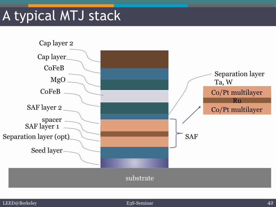
A typical MTJ stack
substrate
Seed layer
Separation layer (opt)
SAF layer 1
SAF layer 2
spacer
SAF
Co/Pt multilayer
Co/Pt multilayer
Ru
CoFeB
CoFeB
MgOSeparation layerTa, W
Cap layer
Cap layer 2

LEED@Berkeley E3S-Seminar 43
Etch issues for high density MRAM
substrate
Physical etching creates sidewalls
![Angle Modulated Systems - · PDF fileAngle Modulated Systems 1. Consider an FM wave ( )=cos[2𝜋 𝑐 +𝛽1sin2𝜋 1 +𝛽22𝜋 2 ] The maximum deviation of the instantaneous frequency](https://img.pdfslide.us/doc/110x75/5ab8499b7f8b9ac10d8cd1da/angle-modulated-systems-modulated-systems-1-consider-an-fm-wave-cos2.jpg)


![The Subcellular Localization and Functional Analysis of ... · short sequences: onesequence formsan 𝛼-helix structure, whichtargetsfibrillarintoCBs[1]andinteractsdirectlywith Nop56[6];theotherisNLS.Thefeatureofthosedomains](https://img.pdfslide.us/doc/110x75/5e770d716e43e15fa122b33d/the-subcellular-localization-and-functional-analysis-of-short-sequences-onesequence.jpg)

![GRETA: WP5 meeting ongoing activities · 2018. 4. 18. · [UNI EN 10344 and 10348] Q h 𝜂𝑔=𝜂 ⋅𝜂 ⋅𝜂 ⋅𝜂 ã With: η g: total seasonal plant efficiency η e: emission](https://img.pdfslide.us/doc/110x75/6132088adfd10f4dd73a2f8b/greta-wp5-meeting-ongoing-activities-2018-4-18-uni-en-10344-and-10348-q.jpg)
![O-[3-18F-fluoropropyl]-𝛼-methyl Tyrosine in Mesothelioma ... · for imaging the metabolic activity of cancers is positron emissiontomography(PET)using18F-2-fluoro-2-deoxy-D-glucose](https://img.pdfslide.us/doc/110x75/5e7ae8d894f8f8158a33608d/o-3-18f-fluoropropyl-methyl-tyrosine-in-mesothelioma-for-imaging-the.jpg)


![Chapter 21 - Multi-electron AtomsIn orbital approximation we write He atom ground state as 𝜓= 1 √ 2 𝜓1s(1)𝜓1s(2)[𝛼(2)𝛽(1)−𝛼(1)𝛽(2)] But now you know that electron–electron](https://img.pdfslide.us/doc/110x75/5f0395897e708231d409c5a1/chapter-21-multi-electron-atoms-in-orbital-approximation-we-write-he-atom-ground.jpg)