Embed Size (px)
Citation preview
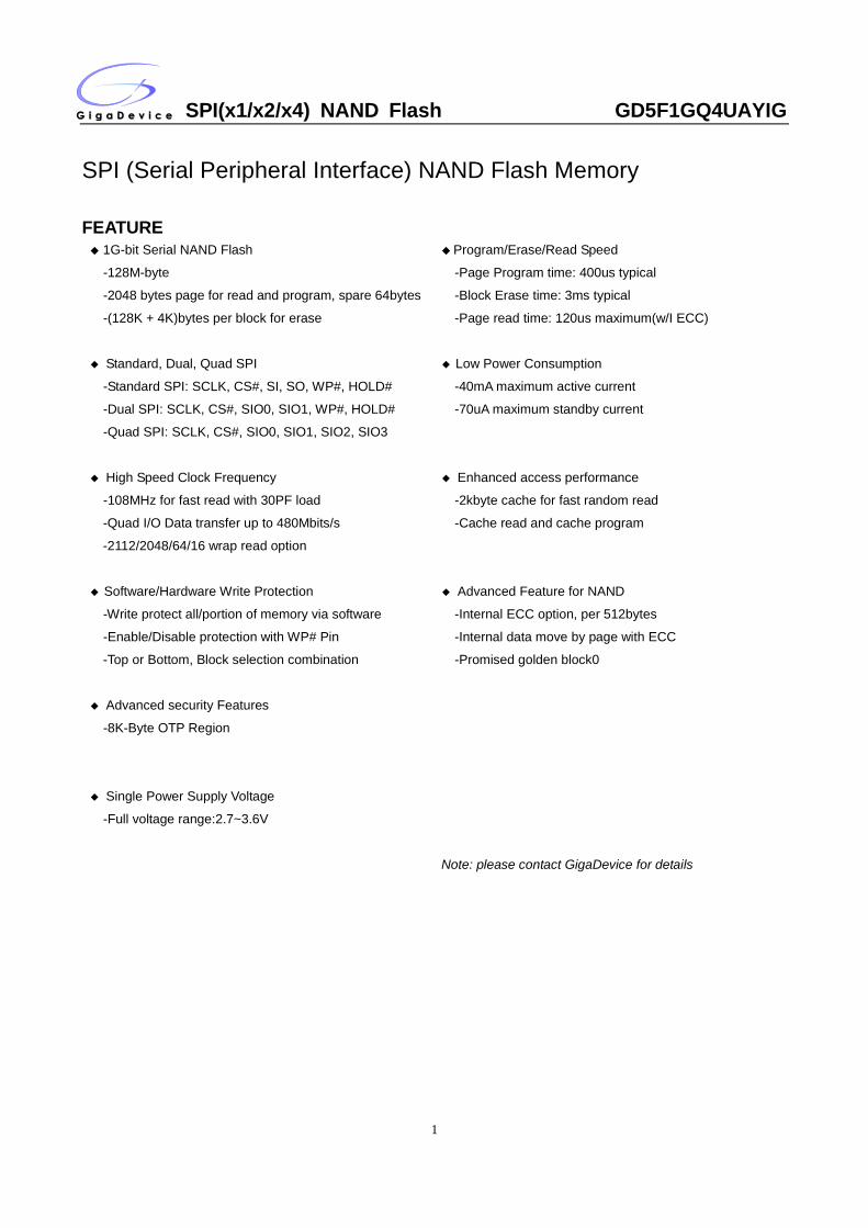
SPI(x1/x2/x4) NAND Flash GD5F1GQ4UAYIG
1
SPI (Serial Peripheral Interface) NAND Flash Memory
FEATURE ◆ 1G-bit Serial NAND Flash ◆ Program/Erase/Read Speed
-128M-byte -Page Program time: 400us typical
-2048 bytes page for read and program, spare 64bytes -Block Erase time: 3ms typical
-(128K + 4K)bytes per block for erase -Page read time: 120us maximum(w/I ECC)
◆ Standard, Dual, Quad SPI ◆ Low Power Consumption
-Standard SPI: SCLK, CS#, SI, SO, WP#, HOLD# -40mA maximum active current
-Dual SPI: SCLK, CS#, SIO0, SIO1, WP#, HOLD# -70uA maximum standby current
-Quad SPI: SCLK, CS#, SIO0, SIO1, SIO2, SIO3
◆ High Speed Clock Frequency ◆ Enhanced access performance
-108MHz for fast read with 30PF load -2kbyte cache for fast random read
-Quad I/O Data transfer up to 480Mbits/s -Cache read and cache program
-2112/2048/64/16 wrap read option
◆ Software/Hardware Write Protection ◆ Advanced Feature for NAND
-Write protect all/portion of memory via software -Internal ECC option, per 512bytes
-Enable/Disable protection with WP# Pin -Internal data move by page with ECC
-Top or Bottom, Block selection combination -Promised golden block0
◆ Advanced security Features
-8K-Byte OTP Region
◆ Single Power Supply Voltage
-Full voltage range:2.7~3.6V
Note: please contact GigaDevice for details
SPI(x1/x2/x4) NAND Flash GD5F1GQ4UAYIG
2
GENERAL DESCRIPTION SPI (Serial Peripheral Interface) NAND Flash provides an ultra cost-effective while high density non-volatile memory
storage solution for embedded systems, based on an industry-standard NAND Flash memory core. It is an attractive
alternative to SPI-NOR and standard parallel NAND Flash, with advanced features:
• Total pin count is 8, including VCC and GND
• Density range from 256Mbit to 8Gbit
• Superior write performance and cost per bit over SPI-NOR
• Significant low cost than parallel NAND
This low-pin-count NAND Flash memory follows the industry-standard serial peripheral interface, and always
remains the same pinout from one density to another. The command sets resemble common SPI-NOR command sets,
modified to handle NAND specific functions and added new features. GigaDevice SPI NAND is an easy-to-integrate
NAND Flash memory, with specified designed features to ease host management:
• User-selectable internal ECC. ECC code is generated internally during a page program operation. When a page is
read to the cache register, the ECC code is detect and correct the errors when necessary. The 64-bytes spare area is
available even when internal ECC enabled. The device outputs corrected data and returns an ECC error status.
• Assistant Block Management. With corresponding options set, the device can prohibit the Bad Block from being
erased. This option features favor the block management convenience and enhance the performance.
• Internal data move or copy back with internal ECC. The device can be easily refreshed and manage garbage
collection task, without need of shift in and out of data.
• Power on Read with internal ECC. The device will automatically read first page of fist block to cache after power
on, then host can directly read data from cache for easy boot. Also the data is promised correctly by internal ECC.
It is programmed and read in page-based operations, and erased in block-based operations. Data is transferred to or
from the NAND Flash memory array, page by page, to a data register and a cache register. The cache register is closest to
I/O control circuits and acts as a data buffer for the I/O data; the data register is closest to the memory array and acts as a
data buffer for the NAND Flash memory array operation. The cache register functions as the buffer memory to enable
page and random data READ/WRITE and copy back operations. These devices also use a SPI status register that reports
the status of device operation.
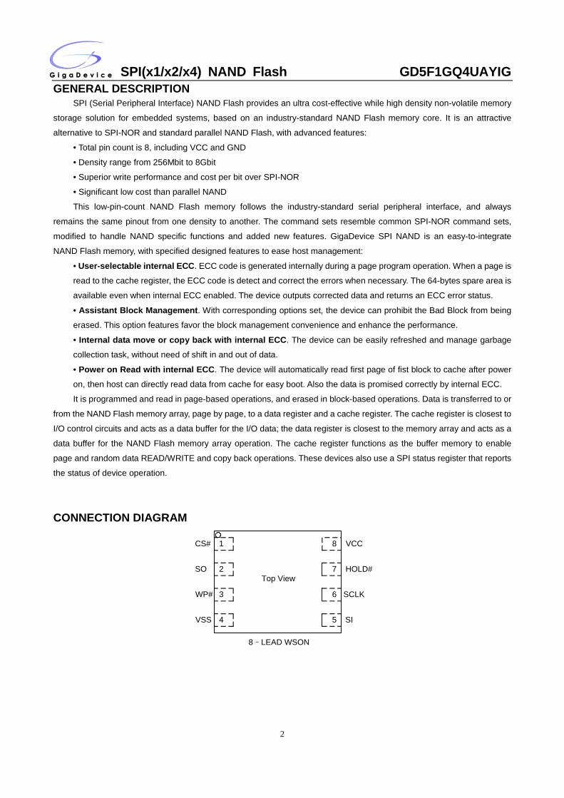
CONNECTION DIAGRAM
CS#
SO
WP#
VSS
Top View
VCC
HOLD#
SCLK
SI
8–LEAD WSON
1
2
3
4 5
6
7
8
SPI(x1/x2/x4) NAND Flash GD5F1GQ4UAYIG
3
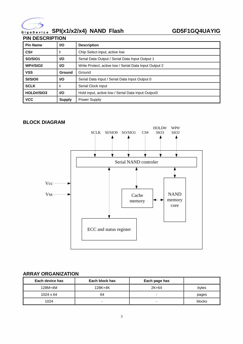
PIN DESCRIPTION Pin Name I/O Description
CS# I Chip Select input, active low
SO/SIO1 I/O Serial Data Output / Serial Data Input Output 1
WP#/SIO2 I/O Write Protect, active low / Serial Data Input Output 2
VSS Ground Ground
SI/SIO0 I/O Serial Data Input / Serial Data Input Output 0
SCLK I Serial Clock input
HOLD#/SIO3 I/O Hold input, active low / Serial Data Input Output3
VCC Supply Power Supply
BLOCK DIAGRAM
Serial NAND controler
Cache memory
NAND memory
core
ECC and status register
Vcc
Vss
SCLK SI/SIO0 SO/SIO1 CS#HOLD#/
SIO3WP#/SIO2
ARRAY ORGANIZATION
Each device has Each block has Each page has
128M+4M 128K+4K 2K+64 bytes
1024 x 64 64 - pages
1024 - - blocks
SPI(x1/x2/x4) NAND Flash GD5F1GQ4UAYIG
4
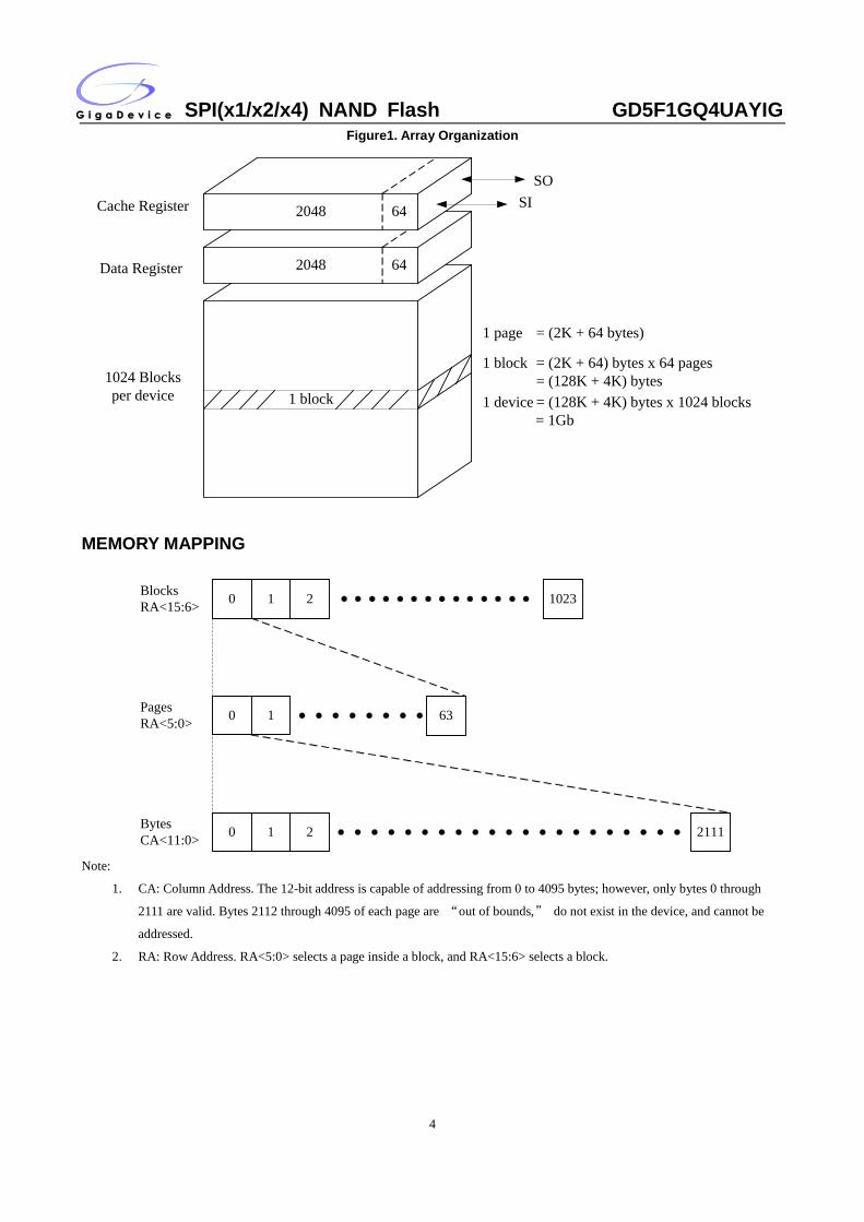
Figure1. Array Organization
2048 64
2048 64
1 block
1 block = (2K + 64) bytes x 64 pages = (128K + 4K) bytes
1 page = (2K + 64 bytes)
1 device = (128K + 4K) bytes x 1024 blocks = 1Gb
Cache Register
Data Register
1024 Blocksper device
SOSI
MEMORY MAPPING
0 1 2 1023
0 1 63
0 1 2 2111
BlocksRA<15:6>
PagesRA<5:0>
BytesCA<11:0>
Note:
1. CA: Column Address. The 12-bit address is capable of addressing from 0 to 4095 bytes; however, only bytes 0 through
2111 are valid. Bytes 2112 through 4095 of each page are “out of bounds,” do not exist in the device, and cannot be
addressed.
2. RA: Row Address. RA<5:0> selects a page inside a block, and RA<15:6> selects a block.
SPI(x1/x2/x4) NAND Flash GD5F1GQ4UAYIG
5
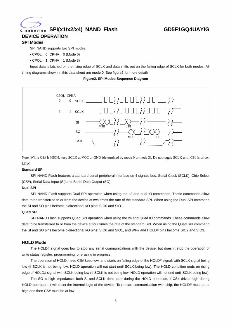
DEVICE OPERATION SPI Modes
SPI NAND supports two SPI modes:
• CPOL = 0, CPHA = 0 (Mode 0)
• CPOL = 1, CPHA = 1 (Mode 3)
Input data is latched on the rising edge of SCLK and data shifts out on the falling edge of SCLK for both modes. All
timing diagrams shown in this data sheet are mode 0. See figure2 for more details.
Figure2. SPI Modes Sequence Diagram
CS#
SCLK
SCLK
SI
SO
CPOL CPHA00
11
MSB LSB
MSB LSB
Note: While CS# is HIGH, keep SCLK at VCC or GND (determined by mode 0 or mode 3). Do not toggle SCLK until CS# is driven
LOW.
Standard SPI SPI NAND Flash features a standard serial peripheral interface on 4 signals bus: Serial Clock (SCLK), Chip Select
(CS#), Serial Data Input (SI) and Serial Data Output (SO).
Dual SPI SPI NAND Flash supports Dual SPI operation when using the x2 and dual IO commands. These commands allow
data to be transferred to or from the device at two times the rate of the standard SPI. When using the Dual SPI command
the SI and SO pins become bidirectional I/O pins: SIO0 and SIO1.
Quad SPI SPI NAND Flash supports Quad SPI operation when using the x4 and Quad IO commands. These commands allow
data to be transferred to or from the device at four times the rate of the standard SPI. When using the Quad SPI command
the SI and SO pins become bidirectional I/O pins: SIO0 and SIO1, and WP# and HOLD# pins become SIO2 and SIO3.
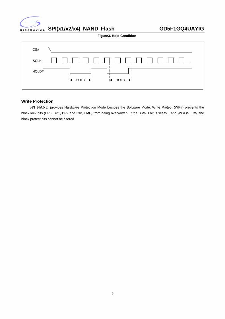
HOLD Mode
The HOLD# signal goes low to stop any serial communications with the device, but doesn’t stop the operation of
write status register, programming, or erasing in progress.
The operation of HOLD, need CS# keep low, and starts on falling edge of the HOLD# signal, with SCLK signal being
low (if SCLK is not being low, HOLD operation will not start until SCLK being low). The HOLD condition ends on rising
edge of HOLD# signal with SCLK being low (If SCLK is not being low, HOLD operation will not end until SCLK being low).
The SO is high impedance, both SI and SCLK don’t care during the HOLD operation, if CS# drives high during
HOLD operation, it will reset the internal logic of the device. To re-start communication with chip, the HOLD# must be at
high and then CS# must be at low.
SPI(x1/x2/x4) NAND Flash GD5F1GQ4UAYIG
6
Figure3. Hold Condition
HOLD HOLD
CS#
SCLK
HOLD#
Write Protection
SPI NAND provides Hardware Protection Mode besides the Software Mode. Write Protect (WP#) prevents the
block lock bits (BP0, BP1, BP2 and INV, CMP) from being overwritten. If the BRWD bit is set to 1 and WP# is LOW, the
block protect bits cannot be altered.
SPI(x1/x2/x4) NAND Flash GD5F1GQ4UAYIG
7
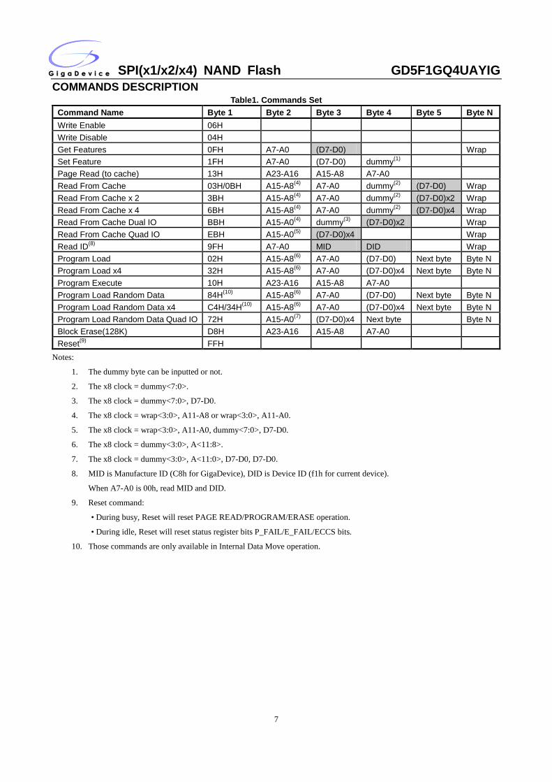
COMMANDS DESCRIPTION Table1. Commands Set
Command Name Byte 1 Byte 2 Byte 3 Byte 4 Byte 5 Byte N Write Enable 06H Write Disable 04H Get Features 0FH A7-A0 (D7-D0) Wrap Set Feature 1FH A7-A0 (D7-D0) dummy(1) Page Read (to cache) 13H A23-A16 A15-A8 A7-A0 Read From Cache 03H/0BH A15-A8(4) A7-A0 dummy(2) (D7-D0) Wrap Read From Cache x 2 3BH A15-A8(4) A7-A0 dummy(2) (D7-D0)x2 Wrap Read From Cache x 4 6BH A15-A8(4) A7-A0 dummy(2) (D7-D0)x4 Wrap Read From Cache Dual IO BBH A15-A0(4) dummy(3) (D7-D0)x2 Wrap Read From Cache Quad IO EBH A15-A0(5) (D7-D0)x4 Wrap Read ID(8) 9FH A7-A0 MID DID Wrap Program Load 02H A15-A8(6) A7-A0 (D7-D0) Next byte Byte N Program Load x4 32H A15-A8(6) A7-A0 (D7-D0)x4 Next byte Byte N Program Execute 10H A23-A16 A15-A8 A7-A0 Program Load Random Data 84H(10) A15-A8(6) A7-A0 (D7-D0) Next byte Byte N Program Load Random Data x4 C4H/34H(10) A15-A8(6) A7-A0 (D7-D0)x4 Next byte Byte N Program Load Random Data Quad IO 72H A15-A0(7) (D7-D0)x4 Next byte Byte N Block Erase(128K) D8H A23-A16 A15-A8 A7-A0 Reset(9) FFH
Notes:
1. The dummy byte can be inputted or not.
2. The x8 clock = dummy<7:0>.
3. The x8 clock = dummy<7:0>, D7-D0.
4. The x8 clock = wrap<3:0>, A11-A8 or wrap<3:0>, A11-A0.
5. The x8 clock = wrap<3:0>, A11-A0, dummy<7:0>, D7-D0.
6. The x8 clock = dummy<3:0>, A<11:8>.
7. The x8 clock = dummy<3:0>, A<11:0>, D7-D0, D7-D0.
8. MID is Manufacture ID (C8h for GigaDevice), DID is Device ID (f1h for current device).
When A7-A0 is 00h, read MID and DID.
9. Reset command:
• During busy, Reset will reset PAGE READ/PROGRAM/ERASE operation.
• During idle, Reset will reset status register bits P_FAIL/E_FAIL/ECCS bits.
10. Those commands are only available in Internal Data Move operation.
SPI(x1/x2/x4) NAND Flash GD5F1GQ4UAYIG
8
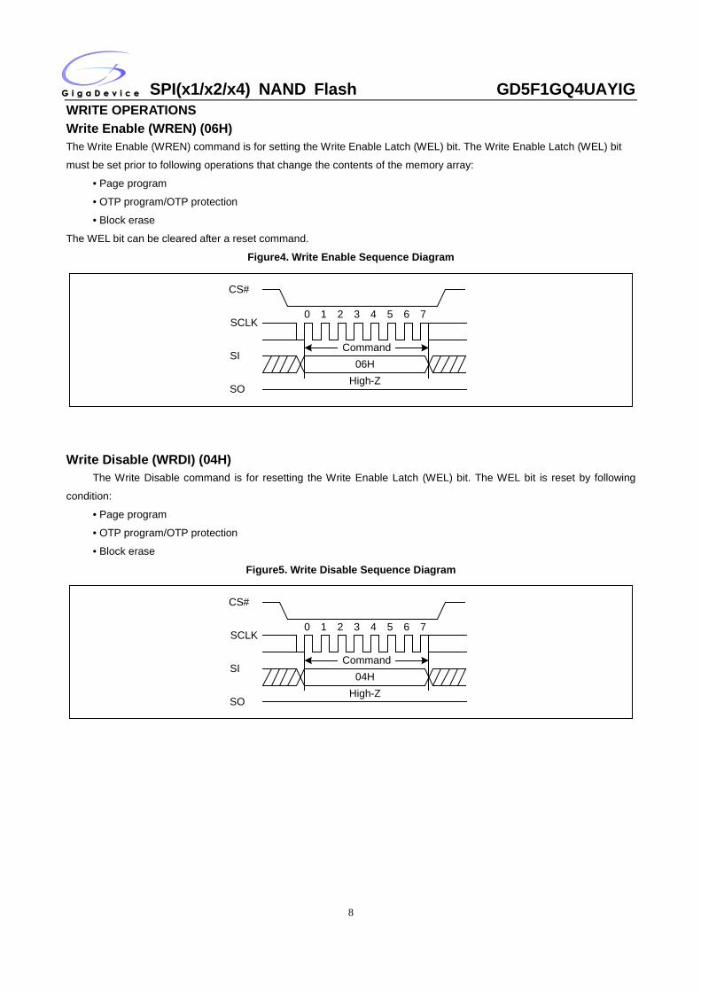
WRITE OPERATIONS Write Enable (WREN) (06H) The Write Enable (WREN) command is for setting the Write Enable Latch (WEL) bit. The Write Enable Latch (WEL) bit
must be set prior to following operations that change the contents of the memory array:
• Page program
• OTP program/OTP protection
• Block erase
The WEL bit can be cleared after a reset command.
Figure4. Write Enable Sequence Diagram
Command
0 1 2 3 4 5 6 7
06H
CS#
SCLK
SI
SOHigh-Z
Write Disable (WRDI) (04H)
The Write Disable command is for resetting the Write Enable Latch (WEL) bit. The WEL bit is reset by following
condition:
• Page program
• OTP program/OTP protection
• Block erase
Figure5. Write Disable Sequence Diagram
Command
0 1 2 3 4 5 6 7
04H
CS#
SCLK
SI
SOHigh-Z
SPI(x1/x2/x4) NAND Flash GD5F1GQ4UAYIG
9
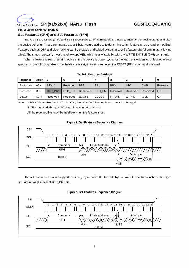
FEATURE OPERATIONS Get Features (0FH) and Set Features (1FH)
The GET FEATURES (0FH) and SET FEATURES (1FH) commands are used to monitor the device status and alter
the device behavior. These commands use a 1-byte feature address to determine which feature is to be read or modified.
Features such as OTP and block locking can be enabled or disabled by setting specific feature bits (shown in the following
table). The status register is mostly read, except WEL, which is a writable bit with the WRITE ENABLE (06H) command.
When a feature is set, it remains active until the device is power cycled or the feature is written to. Unless otherwise
specified in the following table, once the device is set, it remains set, even if a RESET (FFH) command is issued.
Table2. Features Settings
Register Addr. 7 6 5 4 3 2 1 0
Protection A0H BRWD Reserved BP2 BP1 BP0 INV CMP Reserved
Feature B0H OTP_PRT OTP_EN Reserved ECC_EN Reserved Reserved Reserved QE
Status C0H Reserved Reserved ECCS1 ECCS0 P_FAIL E_FAIL WEL OIP
Note: If BRWD is enabled and WP# is LOW, then the block lock register cannot be changed.
If QE is enabled, the quad IO operations can be executed.
All the reserved bits must be held low when the feature is set.
Figure6. Get Features Sequence Diagram
Command
0 1 2 3 4 5 6 7
0FH
CS#
SCLK
SI
SO High-Z
8 9 10 11 12 13 14 15 16 17 18 19 20 21 22 23
7 6 5 4 3 2 1 0
7 6 5 4 3 2 1 0MSB
1 byte address
Data byte
MSB
The set features command supports a dummy byte mode after the data byte as well. The features in the feature byte
B0H are all volatile except OTP_PRT bit.
Figure7. Set Features Sequence Diagram
Command
0 1 2 3 4 5 6 7
1FH
CS#
SCLK
SI
SO High-Z
8 9 10 11 12 13 14 15 16 17 18 19 20 21 22 23
7 6 5 4 3 2 1 0 7 6 5 4 3 2 1 0MSB
1 byte address Data byte
MSB
SPI(x1/x2/x4) NAND Flash GD5F1GQ4UAYIG
10
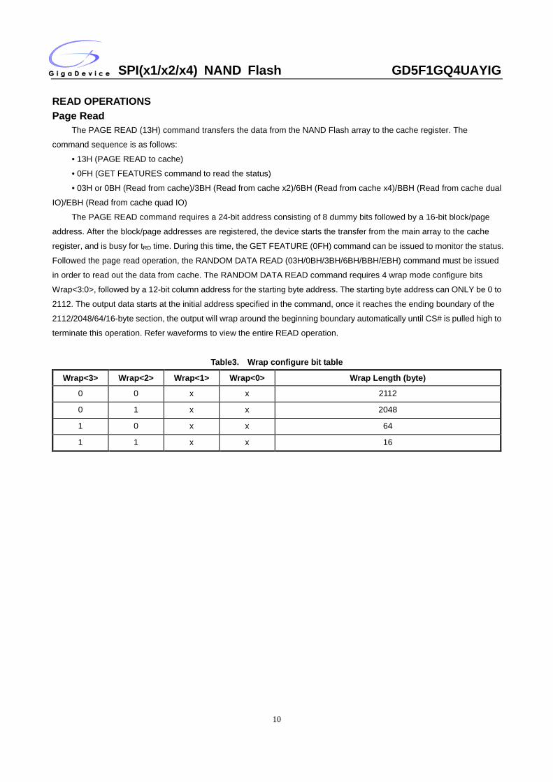
READ OPERATIONS Page Read
The PAGE READ (13H) command transfers the data from the NAND Flash array to the cache register. The
command sequence is as follows:
• 13H (PAGE READ to cache)
• 0FH (GET FEATURES command to read the status)
• 03H or 0BH (Read from cache)/3BH (Read from cache x2)/6BH (Read from cache x4)/BBH (Read from cache dual
IO)/EBH (Read from cache quad IO)
The PAGE READ command requires a 24-bit address consisting of 8 dummy bits followed by a 16-bit block/page
address. After the block/page addresses are registered, the device starts the transfer from the main array to the cache
register, and is busy for tRD time. During this time, the GET FEATURE (0FH) command can be issued to monitor the status.
Followed the page read operation, the RANDOM DATA READ (03H/0BH/3BH/6BH/BBH/EBH) command must be issued
in order to read out the data from cache. The RANDOM DATA READ command requires 4 wrap mode configure bits
Wrap<3:0>, followed by a 12-bit column address for the starting byte address. The starting byte address can ONLY be 0 to
2112. The output data starts at the initial address specified in the command, once it reaches the ending boundary of the
2112/2048/64/16-byte section, the output will wrap around the beginning boundary automatically until CS# is pulled high to
terminate this operation. Refer waveforms to view the entire READ operation.
Table3. Wrap configure bit table
Wrap<3> Wrap<2> Wrap<1> Wrap<0> Wrap Length (byte)
0 0 x x 2112
0 1 x x 2048
1 0 x x 64
1 1 x x 16
SPI(x1/x2/x4) NAND Flash GD5F1GQ4UAYIG
11
Page Read to Cache (13H)
Figure8. Page Read to cache Sequence Diagram
Command
0 1 2 3 4 5 6 7
13H
CS#
SCLK
SI
SO High-Z
8 9 10 28 29 30 31
3 2 1 023 22 21
24-bit address
CS#
Get Feature
0 1 2 3 4 5 6 7
0FH
CS#
SLK
SI
SO High-Z
8 9 10 11 12 13 14 15
7 6 5 4 3 2 1 0
7 6 5 4 3 2 1 0 7
MSB
1 byte address
Data byte
MSB
SCLK
SI
SO
tCS
16 17 18 19 20 21 22 23 24
Read From Cache (03H or 0BH)
Figure10. Read From Cache Sequence Diagram
Command
0 1 2 3 4 5 6 7
03H or 0BH
CS#
SCLK
SI
SO High-Z
8 9 10 11 12 13 14 22 23
3 2 1 00 0A11-0
MSB
26 27 28 2925
6 5 4 3 2 1 0
30 31
Data Out1
24 34 35 36 3733 38 3932
7
6 5 4 3 2 1 07
6 57Data Out2
CS#
SCLK
SI
SOMSB
Dummy Byte
00 11 10
Wrap<3:0>
SPI(x1/x2/x4) NAND Flash GD5F1GQ4UAYIG
12
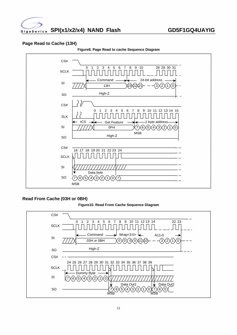
Read From Cache x2 (3BH)
Figure11. Read From Cache x2 Sequence Diagram
Command
0 1 2 3 4 5 6 7
3BH
CS#
SCLK
SI/SIO0
SO/SIO1 High-Z
8 9 10 11 12 13 14 22 23
3 2 1 00 0A11-0
MSB
26 27 28 2925
5 3 1 7 5 3 1
30 31
Data Out1
24 34 35 36 3733 38 3932
7
6 5 4 3 2 1 07
5 37Data Out2
CS#
SCLK
MSB
Dummy Byte
00 11 10
Wrap<3:0>
4 2 0 6 4 2 06 4 26SI/SIO0
SO/SIO1
Read From Cache x4 (6BH)
The Quad Enable bit (QE) of feature (B0[0]) must be set to enable the read from cache x4 command. Figure12. Read From Cache x4 Sequence Diagram
SO(SIO1) High-Z
26 27 28 2925
1 5 1 5 1 5 1
30 31
Byte1
24 34 35 36 3733 38 3932
5
Dummy Byte0 4 0 4 0 4 04 4
5
WP#(SIO2) High-ZHOLD#(SIO3) High-Z
CS#
SCLK
SI(SIO0)
SO(SIO1)
WP#(SIO2)
HOLD#(SIO3)
2 6 2 6 2 6 26 6
3 7 3 7 3 7 37 7Byte2 Byte3 Byte4
Command
0 1 2 3 4 5 6 7
6BH
CS#
SCLK
SI(SIO0)
8 9 10 11 12 13 14 22 23
3 2 1 00 0A11-0
00 11 10
Wrap<3:0>
6 5 4 3 2 1 07
SPI(x1/x2/x4) NAND Flash GD5F1GQ4UAYIG
13
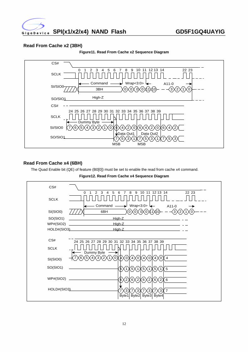
Read From Cache Dual IO (BBH) The Read from Cache Dual I/O command (BBH) is similar to the Read form Cache x2 command (3BH) but with the
capability to input the 4 Wrap bits, followed by a 12-bit column address for the starting byte address and a dummy byte by
SIO0 and SIO1, each bit being latched in during the rising edge of SCLK, then the cache contents are shifted out 2-bit per
clock cycle from SIO0 and SIO1. The first address byte can be at any location. The address increments automatically to
the next higher address after each byte of data shifted out until the boundary wrap bit.
Figure13. Read From Cache Dual IO Sequence Diagram
Command
0 1 2 3 4 5 6 7
BBH
CS#
SCLK
SI(SIO0)
SO(SIO1)
8 9 10 11 12 13 14 15
6 4 2 0 6 4 2 0
16 17 18 19 20 21 22 23
6 4 2 0 6 4 2 0
7 5 3 1 7 5 3 1 7 5 3 1 7 5 3 1A7-0 Dummy Byte1
CS#23 24 25 26 27 28 29 30 31 32 33 34 35 36 37 38 39
SI(SIO0)
SO(SIO1)
6 4 2 0 6 4 2 0 6 4 2 0 6 4 2 0
7 5 3 1 7 5 3 1 7 5 3 1 7 5 3 1
SCLK
6
7Byte2 Byte3 Byte4 Byte5
Wrap<3:0>, A11-8
Read From Cache Quad IO (EBH) The Read from Cache Quad IO command is similar to the Read from Cache x4 command but with the capability to
input the 4 wrap bits, followed a 12-bit column address for the starting byte address and a dummy byte by SIO0, SIO1,
SIO3, SIO4, each bit being latched in during the rising edge of SCLK, then the cache contents are shifted out 4-bit per
clock cycle from SIO0, SIO1, SIO2, SIO3. The first byte addressed can be at any location. The address is automatically
incremented to the next higher address after each byte of data is shifted out until the boundary wrap bit. The Quad Enable
bit (QE) of feature (B0[0]) must be set to enable the read from cache quad IO command. Figure14. Read From Cache Quad IO Sequence Diagram
Command
0 1 2 3 4 5 6 7
EBH
CS#
SCLK
SI(SIO0)
SO(SIO1)
8 9 10 11 12 13 14 15
4 0 4 0 4 0
16 17 18 19 20 21 22 23
4 0 4 0
5 1 5 1 5 1 5 1 5 1
A7-0
6 2 6 2 6 2 6 2 6 2
7 3 7 3 7 3 7 3 7 3
WP#(SIO2)
HOLD#(SIO3)
4
5
6
7
Dummy Byte1 Byte2Wrap<3:0>, A11-A8
SPI(x1/x2/x4) NAND Flash GD5F1GQ4UAYIG
14
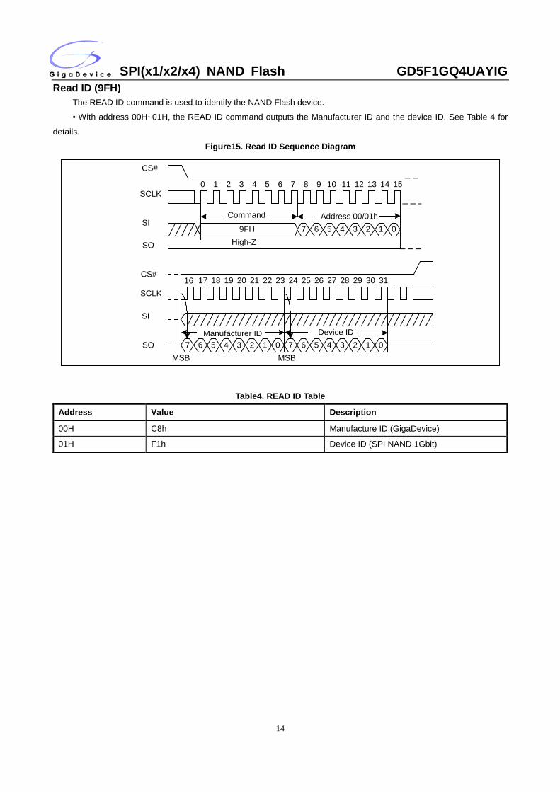
Read ID (9FH) The READ ID command is used to identify the NAND Flash device.
• With address 00H~01H, the READ ID command outputs the Manufacturer ID and the device ID. See Table 4 for
details.
Figure15. Read ID Sequence Diagram
Command
0 1 2 3 4 5 6 7
9FH
CS#
SCLK
SI
SO High-Z
8 9 10 11
Address 00/01h
MSB
18 19 20 2117
6 5 4 3 2 1 0
22 2316 26 27 28 2925 30 3124
7Device ID
CS#
SCLK
SI
SOMSB
Manufacturer ID6 5 4 3 2 1 07
6 5 4 3 2 1 07
12 13 14 15
Table4. READ ID Table Address Value Description
00H C8h Manufacture ID (GigaDevice)
01H F1h Device ID (SPI NAND 1Gbit)
SPI(x1/x2/x4) NAND Flash GD5F1GQ4UAYIG
15
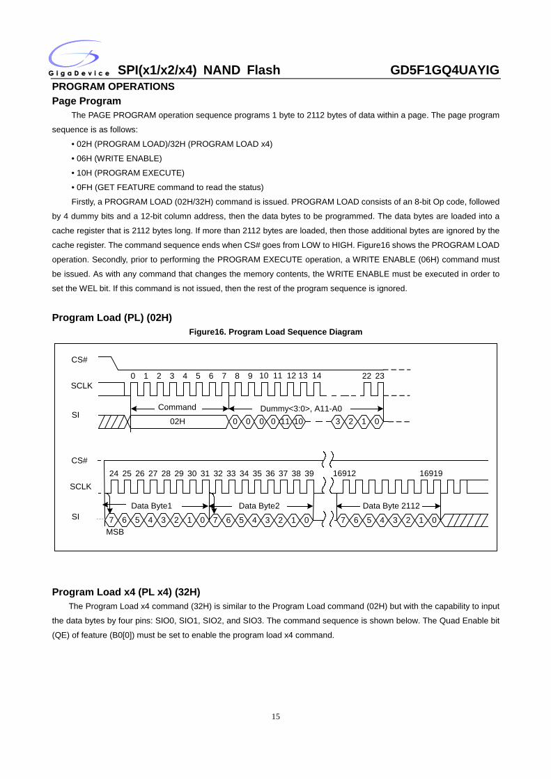
PROGRAM OPERATIONS Page Program
The PAGE PROGRAM operation sequence programs 1 byte to 2112 bytes of data within a page. The page program
sequence is as follows:
• 02H (PROGRAM LOAD)/32H (PROGRAM LOAD x4)
• 06H (WRITE ENABLE)
• 10H (PROGRAM EXECUTE)
• 0FH (GET FEATURE command to read the status)
Firstly, a PROGRAM LOAD (02H/32H) command is issued. PROGRAM LOAD consists of an 8-bit Op code, followed
by 4 dummy bits and a 12-bit column address, then the data bytes to be programmed. The data bytes are loaded into a
cache register that is 2112 bytes long. If more than 2112 bytes are loaded, then those additional bytes are ignored by the
cache register. The command sequence ends when CS# goes from LOW to HIGH. Figure16 shows the PROGRAM LOAD
operation. Secondly, prior to performing the PROGRAM EXECUTE operation, a WRITE ENABLE (06H) command must
be issued. As with any command that changes the memory contents, the WRITE ENABLE must be executed in order to
set the WEL bit. If this command is not issued, then the rest of the program sequence is ignored.
Program Load (PL) (02H) Figure16. Program Load Sequence Diagram
Command
0 1 2 3 4 5 6 7
02H
CS#
SCLK
SI
8 9 10 11 12 13 14 22 23
3 2 1 00 0
MSB
26 27 28 2925
6 5 4 3 2 1 0
30 3124 34 35 36 3733 38 3932
76 5 4 3 2 1 07
CS#
SCLK
SIData Byte1
00 11 10
Data Byte2
6 5 4 3 2 1 07
Data Byte 2112
16912 16919
Dummy<3:0>, A11-A0
Program Load x4 (PL x4) (32H)
The Program Load x4 command (32H) is similar to the Program Load command (02H) but with the capability to input
the data bytes by four pins: SIO0, SIO1, SIO2, and SIO3. The command sequence is shown below. The Quad Enable bit
(QE) of feature (B0[0]) must be set to enable the program load x4 command.
SPI(x1/x2/x4) NAND Flash GD5F1GQ4UAYIG
16
Figure17. Program Load x4 Sequence Diagram
Command
0 1 2 3 4 5 6 7
32H
CS#
SCLK8 9 10 20 21 22 23
3 2 1 015 14 13
24 25 26 27
4 0
28 29 30 31
SI(SIO0)
SO(SIO1)
WP#(SIO2)
HOLD#(SIO3)
5 1
6 2
7 3
4 0
5 1
6 2
7 3
4 0
5 1
6 2
7 3
4 0
5 1
6 2
7 3
Byte1 Byte2
CS#
SCLK
SI(SIO0)
SO(SIO1)
WP#(SIO2)
HOLD#(SIO3)
34 35 36 3733 38 3932 42 43 44 4541 46 4740
4 0
5 1
6 2
7 3
4 0
5 1
6 2
7 3
4 0
5 1
6 2
7 3
4 0
5 1
6 2
7 3
4 0
5 1
6 2
7 3
4 0
5 1
6 2
7 3
4 0
5 1
6 2
7 3
Byte114 0
5 1
6 2
7 3
Byte124 0
5 1
6 2
7 3
4 0
5 1
6 2
7 3
4 0
5 1
6 2
7 3
4 0
5 1
6 2
7 3
Byte2112
Byte2111
Dummy<3:0>, A11-A0
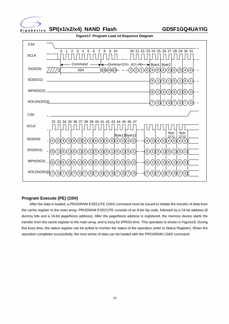
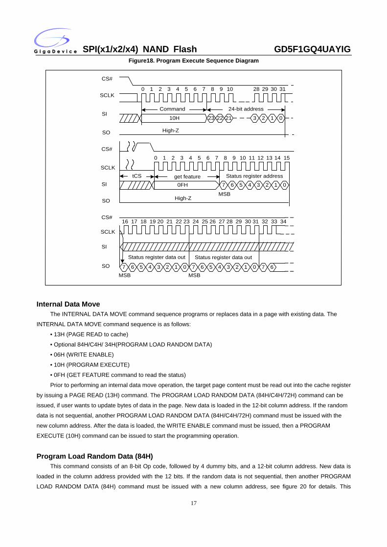
Program Execute (PE) (10H)
After the data is loaded, a PROGRAM EXECUTE (10H) command must be issued to initiate the transfer of data from
the cache register to the main array. PROGRAM EXECUTE consists of an 8-bit Op code, followed by a 24-bit address (8
dummy bits and a 16-bit page/block address). After the page/block address is registered, the memory device starts the
transfer from the cache register to the main array, and is busy for tPROG time. This operation is shown in Figure18. During
this busy time, the status register can be polled to monitor the status of the operation (refer to Status Register). When the
operation completes successfully, the next series of data can be loaded with the PROGRAM LOAD command.
SPI(x1/x2/x4) NAND Flash GD5F1GQ4UAYIG
17
Figure18. Program Execute Sequence Diagram
Command
0 1 2 3 4 5 6 7
10H
CS#
SCLK
SI
SO High-Z
8 9 10 28 29 30 31
3 2 1 023 22 21
24-bit address
CS#
get feature
0 1 2 3 4 5 6 7
0FH
CS#
SCLK
SI
SO High-Z
8 9 10 11 12 13 14 15
7 6 5 4 3 2 1 0
7 6 5 4 3 2 1 0
MSB
Status register address
Status register data out
MSB
SCLK
SI
SO
tCS
16 17 18 19 20 21 22 23 24 25 26 27 28 29 30 31 32 33 34
7 6 5 4 3 2 1 0
Status register data out
7 6MSB
Internal Data Move The INTERNAL DATA MOVE command sequence programs or replaces data in a page with existing data. The
INTERNAL DATA MOVE command sequence is as follows:
• 13H (PAGE READ to cache)
• Optional 84H/C4H/ 34H(PROGRAM LOAD RANDOM DATA)
• 06H (WRITE ENABLE)
• 10H (PROGRAM EXECUTE)
• 0FH (GET FEATURE command to read the status)
Prior to performing an internal data move operation, the target page content must be read out into the cache register
by issuing a PAGE READ (13H) command. The PROGRAM LOAD RANDOM DATA (84H/C4H/72H) command can be
issued, if user wants to update bytes of data in the page. New data is loaded in the 12-bit column address. If the random
data is not sequential, another PROGRAM LOAD RANDOM DATA (84H/C4H/72H) command must be issued with the
new column address. After the data is loaded, the WRITE ENABLE command must be issued, then a PROGRAM
EXECUTE (10H) command can be issued to start the programming operation.
Program Load Random Data (84H) This command consists of an 8-bit Op code, followed by 4 dummy bits, and a 12-bit column address. New data is
loaded in the column address provided with the 12 bits. If the random data is not sequential, then another PROGRAM
LOAD RANDOM DATA (84H) command must be issued with a new column address, see figure 20 for details. This
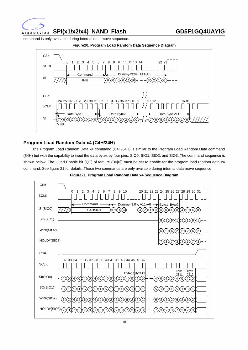
SPI(x1/x2/x4) NAND Flash GD5F1GQ4UAYIG
18
command is only available during internal data move sequence.
Figure20. Program Load Random Data Sequence Diagram
Command
0 1 2 3 4 5 6 7
84H
CS#
SCLK
SI
8 9 10 11 12 13 14 22 23
3 2 1 00 0
MSB
26 27 28 2925
6 5 4 3 2 1 0
30 3124 34 35 36 3733 38 3932
76 5 4 3 2 1 07
CS#
SCLK
SIData Byte1
00 11 10
Data Byte2
6 5 4 3 2 1 07
Data Byte 2112
16912 16919
Dummy<3:0>, A11-A0
Program Load Random Data x4 (C4H/34H)
The Program Load Random Data x4 command (C4H/34H) is similar to the Program Load Random Data command
(84H) but with the capability to input the data bytes by four pins: SIO0, SIO1, SIO2, and SIO3. The command sequence is
shown below. The Quad Enable bit (QE) of feature (B0[0]) must be set to enable for the program load random data x4
command. See figure 21 for details. Those two commands are only available during internal data move sequence.
Figure21. Program Load Random Data x4 Sequence Diagram
Command
0 1 2 3 4 5 6 7
C4H/34H
CS#
SCLK8 9 10 20 21 22 23
3 2 1 015 14 13
24 25 26 27
4 0
28 29 30 31
SI(SIO0)
SO(SIO1)
WP#(SIO2)
HOLD#(SIO3)
5 1
6 2
7 3
4 0
5 1
6 2
7 3
4 0
5 1
6 2
7 3
4 0
5 1
6 2
7 3
Byte1 Byte2
CS#
SCLK
SI(SIO0)
SO(SIO1)
WP#(SIO2)
HOLD#(SIO3)
34 35 36 3733 38 3932 42 43 44 4541 46 4740
4 0
5 1
6 2
7 3
4 0
5 1
6 2
7 3
4 0
5 1
6 2
7 3
4 0
5 1
6 2
7 3
4 0
5 1
6 2
7 3
4 0
5 1
6 2
7 3
4 0
5 1
6 2
7 3
Byte114 0
5 1
6 2
7 3
Byte124 0
5 1
6 2
7 3
4 0
5 1
6 2
7 3
4 0
5 1
6 2
7 3
4 0
5 1
6 2
7 3
Byte2112
Byte2111
Dummy<3:0>, A11-A0
SPI(x1/x2/x4) NAND Flash GD5F1GQ4UAYIG
19
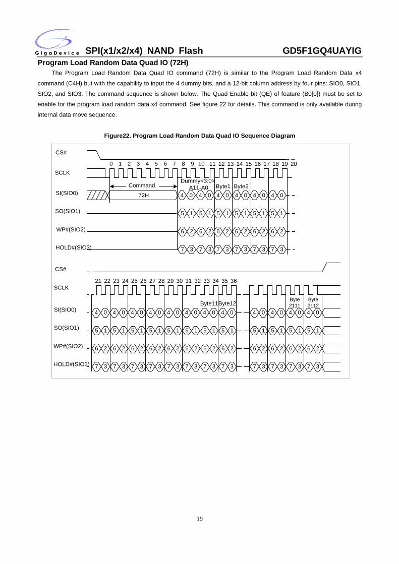
Program Load Random Data Quad IO (72H) The Program Load Random Data Quad IO command (72H) is similar to the Program Load Random Data x4
command (C4H) but with the capability to input the 4 dummy bits, and a 12-bit column address by four pins: SIO0, SIO1,
SIO2, and SIO3. The command sequence is shown below. The Quad Enable bit (QE) of feature (B0[0]) must be set to
enable for the program load random data x4 command. See figure 22 for details. This command is only available during
internal data move sequence.
Figure22. Program Load Random Data Quad IO Sequence Diagram
Command
0 1 2 3 4 5 6 7
72H
CS#
8 9 10 13 14 15 16 17 18 19 20
4 0SI(SIO0)
SO(SIO1)
WP#(SIO2)
HOLD#(SIO3)
5 1
6 2
7 3
4 0
5 1
6 2
7 3
4 0
5 1
6 2
7 3
4 0
5 1
6 2
7 3
Byte1 Byte2
CS#
SI(SIO0)
SO(SIO1)
WP#(SIO2)
HOLD#(SIO3)
23 24 25 2622 27 2821 31 32 33 3430 35 3629
4 0
5 1
6 2
7 3
4 0
5 1
6 2
7 3
4 0
5 1
6 2
7 3
4 0
5 1
6 2
7 3
4 0
5 1
6 2
7 3
4 0
5 1
6 2
7 3
4 0
5 1
6 2
7 3
Byte114 0
5 1
6 2
7 3
Byte124 0
5 1
6 2
7 3
4 0
5 1
6 2
7 3
4 0
5 1
6 2
7 3
4 0
5 1
6 2
7 3
Byte2112
Byte2111
11 12
4 0
5 1
6 2
7 3
4 0
5 1
6 2
7 3
SCLK
SCLK
Dummy<3:0> A11-A0
SPI(x1/x2/x4) NAND Flash GD5F1GQ4UAYIG
20
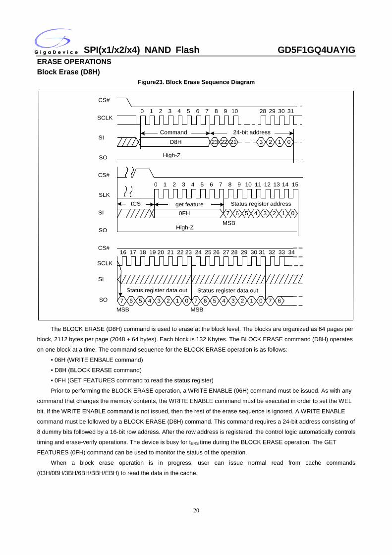
ERASE OPERATIONS Block Erase (D8H)
Figure23. Block Erase Sequence Diagram
Command
0 1 2 3 4 5 6 7
D8H
CS#
SCLK
SI
SO High-Z
8 9 10 28 29 30 31
3 2 1 023 22 21
24-bit address
CS#
get feature
0 1 2 3 4 5 6 7
0FH
CS#
SLK
SI
SO High-Z
8 9 10 11 12 13 14 15
7 6 5 4 3 2 1 0
7 6 5 4 3 2 1 0
MSB
Status register address
Status register data out
MSB
SCLK
SI
SO
tCS
16 17 18 19 20 21 22 23 24 25 26 27 28 29 30 31 32 33 34
7 6 5 4 3 2 1 0
Status register data out
7 6MSB
The BLOCK ERASE (D8H) command is used to erase at the block level. The blocks are organized as 64 pages per
block, 2112 bytes per page (2048 + 64 bytes). Each block is 132 Kbytes. The BLOCK ERASE command (D8H) operates
on one block at a time. The command sequence for the BLOCK ERASE operation is as follows:
• 06H (WRITE ENBALE command)
• D8H (BLOCK ERASE command)
• 0FH (GET FEATURES command to read the status register)
Prior to performing the BLOCK ERASE operation, a WRITE ENABLE (06H) command must be issued. As with any
command that changes the memory contents, the WRITE ENABLE command must be executed in order to set the WEL
bit. If the WRITE ENABLE command is not issued, then the rest of the erase sequence is ignored. A WRITE ENABLE
command must be followed by a BLOCK ERASE (D8H) command. This command requires a 24-bit address consisting of
8 dummy bits followed by a 16-bit row address. After the row address is registered, the control logic automatically controls
timing and erase-verify operations. The device is busy for tERS time during the BLOCK ERASE operation. The GET
FEATURES (0FH) command can be used to monitor the status of the operation.
When a block erase operation is in progress, user can issue normal read from cache commands
(03H/0BH/3BH/6BH/BBH/EBH) to read the data in the cache.
SPI(x1/x2/x4) NAND Flash GD5F1GQ4UAYIG
21
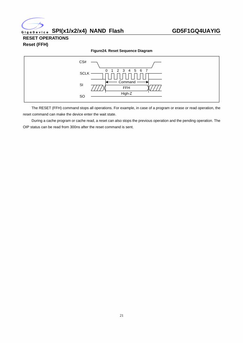
RESET OPERATIONS Reset (FFH)
Figure24. Reset Sequence Diagram
Command
0 1 2 3 4 5 6 7
FFH
CS#
SCLK
SI
SOHigh-Z
The RESET (FFH) command stops all operations. For example, in case of a program or erase or read operation, the
reset command can make the device enter the wait state.
During a cache program or cache read, a reset can also stops the previous operation and the pending operation. The
OIP status can be read from 300ns after the reset command is sent.
SPI(x1/x2/x4) NAND Flash GD5F1GQ4UAYIG
22
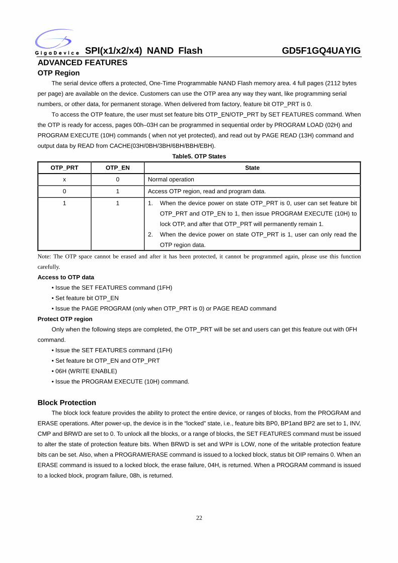
ADVANCED FEATURES OTP Region
The serial device offers a protected, One-Time Programmable NAND Flash memory area. 4 full pages (2112 bytes
per page) are available on the device. Customers can use the OTP area any way they want, like programming serial
numbers, or other data, for permanent storage. When delivered from factory, feature bit OTP_PRT is 0.
To access the OTP feature, the user must set feature bits OTP_EN/OTP_PRT by SET FEATURES command. When
the OTP is ready for access, pages 00h–03H can be programmed in sequential order by PROGRAM LOAD (02H) and
PROGRAM EXECUTE (10H) commands ( when not yet protected), and read out by PAGE READ (13H) command and
output data by READ from CACHE(03H/0BH/3BH/6BH/BBH/EBH).
Table5. OTP States OTP_PRT OTP_EN State
x 0 Normal operation
0 1 Access OTP region, read and program data.
1 1 1. When the device power on state OTP_PRT is 0, user can set feature bit
OTP_PRT and OTP_EN to 1, then issue PROGRAM EXECUTE (10H) to
lock OTP, and after that OTP_PRT will permanently remain 1.
2. When the device power on state OTP_PRT is 1, user can only read the
OTP region data.
Note: The OTP space cannot be erased and after it has been protected, it cannot be programmed again, please use this function
carefully.
Access to OTP data • Issue the SET FEATURES command (1FH)
• Set feature bit OTP_EN
• Issue the PAGE PROGRAM (only when OTP_PRT is 0) or PAGE READ command
Protect OTP region Only when the following steps are completed, the OTP_PRT will be set and users can get this feature out with 0FH
command.
• Issue the SET FEATURES command (1FH)
• Set feature bit OTP_EN and OTP_PRT
• 06H (WRITE ENABLE)
• Issue the PROGRAM EXECUTE (10H) command.
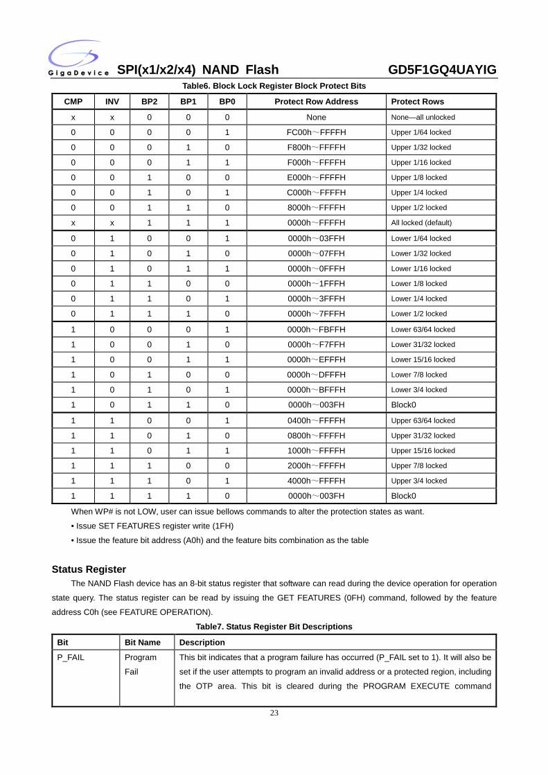
Block Protection
The block lock feature provides the ability to protect the entire device, or ranges of blocks, from the PROGRAM and
ERASE operations. After power-up, the device is in the “locked” state, i.e., feature bits BP0, BP1and BP2 are set to 1, INV,
CMP and BRWD are set to 0. To unlock all the blocks, or a range of blocks, the SET FEATURES command must be issued
to alter the state of protection feature bits. When BRWD is set and WP# is LOW, none of the writable protection feature
bits can be set. Also, when a PROGRAM/ERASE command is issued to a locked block, status bit OIP remains 0. When an
ERASE command is issued to a locked block, the erase failure, 04H, is returned. When a PROGRAM command is issued
to a locked block, program failure, 08h, is returned.
SPI(x1/x2/x4) NAND Flash GD5F1GQ4UAYIG
23
Table6. Block Lock Register Block Protect Bits CMP INV BP2 BP1 BP0 Protect Row Address Protect Rows
x x 0 0 0 None None—all unlocked
0 0 0 0 1 FC00h~FFFFH Upper 1/64 locked
0 0 0 1 0 F800h~FFFFH Upper 1/32 locked
0 0 0 1 1 F000h~FFFFH Upper 1/16 locked
0 0 1 0 0 E000h~FFFFH Upper 1/8 locked
0 0 1 0 1 C000h~FFFFH Upper 1/4 locked
0 0 1 1 0 8000h~FFFFH Upper 1/2 locked
x x 1 1 1 0000h~FFFFH All locked (default)
0 1 0 0 1 0000h~03FFH Lower 1/64 locked
0 1 0 1 0 0000h~07FFH Lower 1/32 locked
0 1 0 1 1 0000h~0FFFH Lower 1/16 locked
0 1 1 0 0 0000h~1FFFH Lower 1/8 locked
0 1 1 0 1 0000h~3FFFH Lower 1/4 locked
0 1 1 1 0 0000h~7FFFH Lower 1/2 locked
1 0 0 0 1 0000h~FBFFH Lower 63/64 locked
1 0 0 1 0 0000h~F7FFH Lower 31/32 locked
1 0 0 1 1 0000h~EFFFH Lower 15/16 locked
1 0 1 0 0 0000h~DFFFH Lower 7/8 locked
1 0 1 0 1 0000h~BFFFH Lower 3/4 locked
1 0 1 1 0 0000h~003FH Block0
1 1 0 0 1 0400h~FFFFH Upper 63/64 locked
1 1 0 1 0 0800h~FFFFH Upper 31/32 locked
1 1 0 1 1 1000h~FFFFH Upper 15/16 locked
1 1 1 0 0 2000h~FFFFH Upper 7/8 locked
1 1 1 0 1 4000h~FFFFH Upper 3/4 locked
1 1 1 1 0 0000h~003FH Block0
When WP# is not LOW, user can issue bellows commands to alter the protection states as want.
• Issue SET FEATURES register write (1FH)
• Issue the feature bit address (A0h) and the feature bits combination as the table
Status Register The NAND Flash device has an 8-bit status register that software can read during the device operation for operation
state query. The status register can be read by issuing the GET FEATURES (0FH) command, followed by the feature
address C0h (see FEATURE OPERATION).
Table7. Status Register Bit Descriptions Bit Bit Name Description
P_FAIL Program
Fail
This bit indicates that a program failure has occurred (P_FAIL set to 1). It will also be
set if the user attempts to program an invalid address or a protected region, including
the OTP area. This bit is cleared during the PROGRAM EXECUTE command
SPI(x1/x2/x4) NAND Flash GD5F1GQ4UAYIG
24
sequence or a RESET command (P_FAIL = 0).
E_FAIL Erase Fail This bit indicates that an erase failure has occurred (E_FAIL set to 1). It will also be
set if the user attempts to erase a locked region. This bit is cleared (E_FAIL = 0) at the
start of the BLOCK ERASE command sequence or the RESET command.
WEL Write
Enable
Latch
This bit indicates the current status of the write enable latch (WEL) and must be set
(WEL = 1), prior to issuing a PROGRAM EXECUTE or BLOCK ERASE command. It
is set by issuing the WRITE ENABLE command. WEL can also be disabled (WEL =
0), by issuing the WRITE DISABLE command.
OIP Operation
In Progress
This bit is set (OIP = 1 ) when a PROGRAM EXECUTE, PAGE READ, BLOCK
ERASE, or RESET command is executing, indicating the device is busy. When the bit
is 0, the interface is in the ready state.
ECCS1,ECCS0 ECC Status ECCS provides ECC status as follows:
00b = No bit errors were detected during the previous read algorithm.
01b = bit error was detected and corrected, error bit number = 1~7.
10b = bit error was detected and not corrected.
11b = bit error was detected and corrected, error bit number = 8.
ECCS is set to 00b either following a RESET, or at the beginning of the READ. It is
then updated after the device completes a valid READ operation.
ECCS is invalid if internal ECC is disabled (via a SET FEATURES command to reset
ECC_EN to 0).
After power-on RESET, ECC status is set to reflect the contents of block 0, page 0.
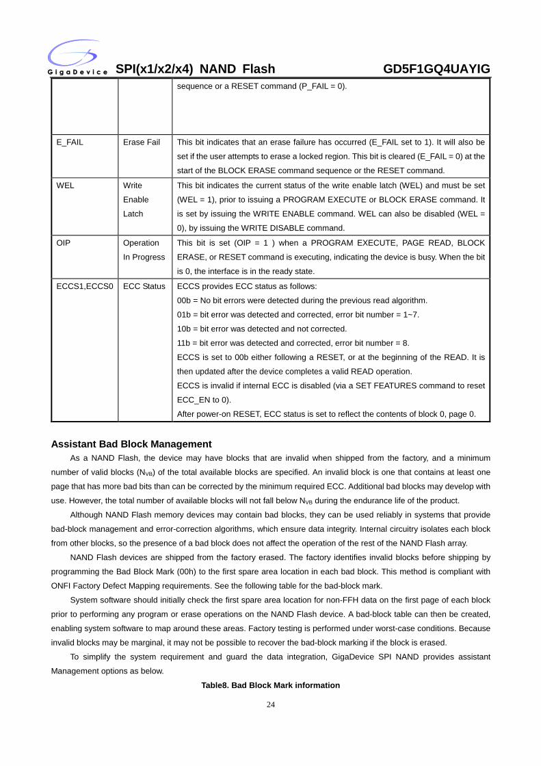
Assistant Bad Block Management
As a NAND Flash, the device may have blocks that are invalid when shipped from the factory, and a minimum
number of valid blocks (NVB) of the total available blocks are specified. An invalid block is one that contains at least one
page that has more bad bits than can be corrected by the minimum required ECC. Additional bad blocks may develop with
use. However, the total number of available blocks will not fall below NVB during the endurance life of the product.
Although NAND Flash memory devices may contain bad blocks, they can be used reliably in systems that provide
bad-block management and error-correction algorithms, which ensure data integrity. Internal circuitry isolates each block
from other blocks, so the presence of a bad block does not affect the operation of the rest of the NAND Flash array.
NAND Flash devices are shipped from the factory erased. The factory identifies invalid blocks before shipping by
programming the Bad Block Mark (00h) to the first spare area location in each bad block. This method is compliant with
ONFI Factory Defect Mapping requirements. See the following table for the bad-block mark.
System software should initially check the first spare area location for non-FFH data on the first page of each block
prior to performing any program or erase operations on the NAND Flash device. A bad-block table can then be created,
enabling system software to map around these areas. Factory testing is performed under worst-case conditions. Because
invalid blocks may be marginal, it may not be possible to recover the bad-block marking if the block is erased.
To simplify the system requirement and guard the data integration, GigaDevice SPI NAND provides assistant
Management options as below.
Table8. Bad Block Mark information
SPI(x1/x2/x4) NAND Flash GD5F1GQ4UAYIG
25
Description Requirement
Minimum number of valid blocks (NVB) 1004
Total available blocks per die 1024
First spare area location Byte 2048
Bad-block mark 00h(use non FFH to check)
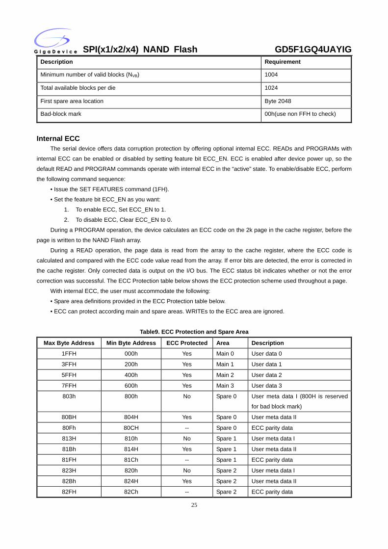
Internal ECC The serial device offers data corruption protection by offering optional internal ECC. READs and PROGRAMs with
internal ECC can be enabled or disabled by setting feature bit ECC_EN. ECC is enabled after device power up, so the
default READ and PROGRAM commands operate with internal ECC in the “active” state. To enable/disable ECC, perform
the following command sequence:
• Issue the SET FEATURES command (1FH).
• Set the feature bit ECC_EN as you want:
1. To enable ECC, Set ECC_EN to 1.
2. To disable ECC, Clear ECC_EN to 0.
During a PROGRAM operation, the device calculates an ECC code on the 2k page in the cache register, before the
page is written to the NAND Flash array.
During a READ operation, the page data is read from the array to the cache register, where the ECC code is
calculated and compared with the ECC code value read from the array. If error bits are detected, the error is corrected in
the cache register. Only corrected data is output on the I/O bus. The ECC status bit indicates whether or not the error
correction was successful. The ECC Protection table below shows the ECC protection scheme used throughout a page.
With internal ECC, the user must accommodate the following:
• Spare area definitions provided in the ECC Protection table below.
• ECC can protect according main and spare areas. WRITEs to the ECC area are ignored.
Table9. ECC Protection and Spare Area
Max Byte Address Min Byte Address ECC Protected Area Description
1FFH 000h Yes Main 0 User data 0
3FFH 200h Yes Main 1 User data 1
5FFH 400h Yes Main 2 User data 2
7FFH 600h Yes Main 3 User data 3
803h 800h No Spare 0 User meta data I (800H is reserved
for bad block mark)
80BH 804H Yes Spare 0 User meta data II
80Fh 80CH -- Spare 0 ECC parity data
813H 810h No Spare 1 User meta data I
81Bh 814H Yes Spare 1 User meta data II
81FH 81Ch -- Spare 1 ECC parity data
823H 820h No Spare 2 User meta data I
82Bh 824H Yes Spare 2 User meta data II
82FH 82Ch -- Spare 2 ECC parity data
SPI(x1/x2/x4) NAND Flash GD5F1GQ4UAYIG
26
833H 830h No Spare 3 User meta data I
83Bh 834H Yes Spare 3 User meta data II
83FH 83Ch -- Spare 3 ECC parity data
Table10. ECC Status
Bit 1 Bit 0 Description 0 0 No errors 0 1 Bit error detected and corrected, error bit number = 1~7 1 0 Bit errors greater than 8 bits detected and not corrected 1 1 Bit error detected and corrected, error bit number = 8
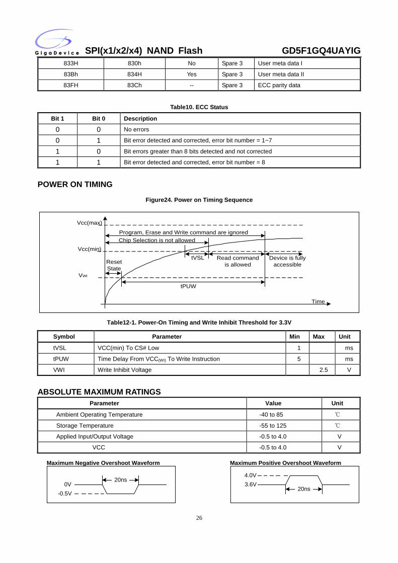
POWER ON TIMING
Figure24. Power on Timing Sequence
Vcc(max)
Vcc(min)
VWI
Reset State
tPUW
tVSL
Chip Selection is not allowedProgram, Erase and Write command are ignored
Read command is allowed
Device is fully accessible
Time
Table12-1. Power-On Timing and Write Inhibit Threshold for 3.3V
Symbol Parameter Min Max Unit
tVSL VCC(min) To CS# Low 1 ms
tPUW Time Delay From VCC(WI) To Write Instruction 5 ms
VWI Write Inhibit Voltage 2.5 V
ABSOLUTE MAXIMUM RATINGS
Parameter Value Unit
Ambient Operating Temperature -40 to 85 ℃
Storage Temperature -55 to 125 ℃
Applied Input/Output Voltage -0.5 to 4.0 V
VCC -0.5 to 4.0 V
0V-0.5V
20ns20ns
4.0V3.6V
Maximum Negative Overshoot Waveform Maximum Positive Overshoot Waveform
SPI(x1/x2/x4) NAND Flash GD5F1GQ4UAYIG
27
CAPACITANCE MEASUREMENT CONDITIONS Symbol Parameter Min Typ Max Unit Conditions
CIN Input Capacitance 6 pF VIN=0V
COUT Output Capacitance 8 pF VOUT=0V
CL Load Capacitance 30 pF
Input Rise And Fall time 5 ns
Input Pulse Voltage 0.2VCC to 0.8VCC V
Input Timing Reference Voltage 0.3VCC to 0.7VCC V
Output Timing Reference Voltage 0.5VCC V
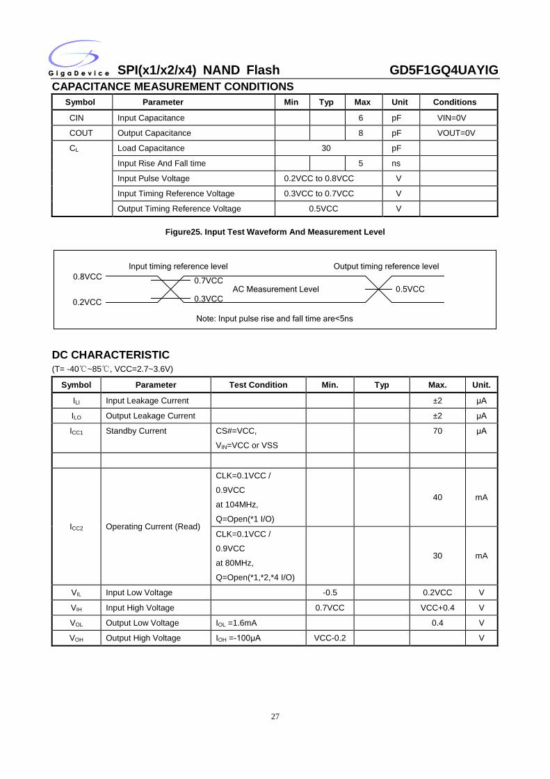
Figure25. Input Test Waveform And Measurement Level
0.8VCC
0.2VCC
0.7VCC
0.3VCC0.5VCCAC Measurement Level
Input timing reference level Output timing reference level
Note: Input pulse rise and fall time are<5ns
DC CHARACTERISTIC (T= -40℃~85℃, VCC=2.7~3.6V)
Symbol Parameter Test Condition Min. Typ Max. Unit.
ILI Input Leakage Current ±2 μA
ILO Output Leakage Current ±2 μA
ICC1 Standby Current CS#=VCC,
VIN=VCC or VSS
70 μA
ICC2 Operating Current (Read)
CLK=0.1VCC /
0.9VCC
at 104MHz,
Q=Open(*1 I/O)
40 mA
CLK=0.1VCC /
0.9VCC
at 80MHz,
Q=Open(*1,*2,*4 I/O)
30 mA
VIL Input Low Voltage -0.5 0.2VCC V
VIH Input High Voltage 0.7VCC VCC+0.4 V
VOL Output Low Voltage IOL =1.6mA 0.4 V
VOH Output High Voltage IOH =-100μA VCC-0.2 V
SPI(x1/x2/x4) NAND Flash GD5F1GQ4UAYIG
28
AC CHARACTERISTICS (T= -40℃~85℃, VCC=2.7~3.6V, CL=30pf)
Symbol Parameter Min. Typ. Max. Unit.
FC Serial Clock Frequency For: all command DC. 108 MHz
tCH Serial Clock High Time 4.5 ns
tCL Serial Clock Low Time 4.5 ns
tCLCH Serial Clock Rise Time (Slew Rate) 0.2 V/ns
tCHCL Serial Clock Fall Time (Slew Rate) 0.2 V/ns
tSLCH CS# Active Setup Time 5 ns
tCHSH CS# Active Hold Time 5 ns
tSHCH CS# Not Active Setup Time 5 ns
tCHSL CS# Not Active Hold Time 5 ns
tSHSL/tCS CS# High Time 20 ns
tSHQZ Output Disable Time 20 ns
tCLQX Output Hold Time 0 ns
tDVCH Data In Setup Time 2 ns
tCHDX Data In Hold Time 2 ns
tHLCH Hold# Low Setup Time (relative to Clock) 5 ns
tHHCH Hold# High Setup Time (relative to Clock) 5 ns
tCHHL Hold# High Hold Time (relative to Clock) 5 ns
tCHHH Hold# Low Hold Time (relative to Clock) 5 ns
tHLQZ Hold# Low To High-Z Output 15 ns
tHHQX Hold# High To Low-Z Output 15 ns
tCLQV Clock Low To Output Valid 8 ns
tWHSL WP# Setup Time Before CS# Low 20 ns
tSHWL WP# Hold Time After CS# High 100 ns
PERFORMANCE TIMING
Symbol Parameter Min. Typ. Max. Unit.
tRST CS# High To Next Command After Reset(FFh) 500 us
tRD Read From Array 120 us
tPROG Page Programming Time 0.4 0.7 ms
tBERS Block Erase Time 3 5 ms
SPI(x1/x2/x4) NAND Flash GD5F1GQ4UAYIG
29
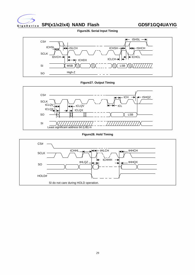
Figure26. Serial Input Timing
SCLK
CS#
SI MSB
SO High-Z
LSB
tCHSL tSLCH
tDVCHtCHDX
tSHCHtCHSH
tCHCLtCLCH
tSHSL
Figure27. Output Timing
CS#
SCLK
SO
SILeast significant address bit (LIB) in
tCLQVtCLQX tCLQX
tCLQV
tCH
tCL
tSHQZ
LSB
Figure28. Hold Timing
CS#
SCLK
SO
HOLD#
tCHHL
tHLQZ
tHLCH
tCHHH
tHHCH
tHHQX
SI do not care during HOLD operation.
SPI(x1/x2/x4) NAND Flash GD5F1GQ4UAYIG
30
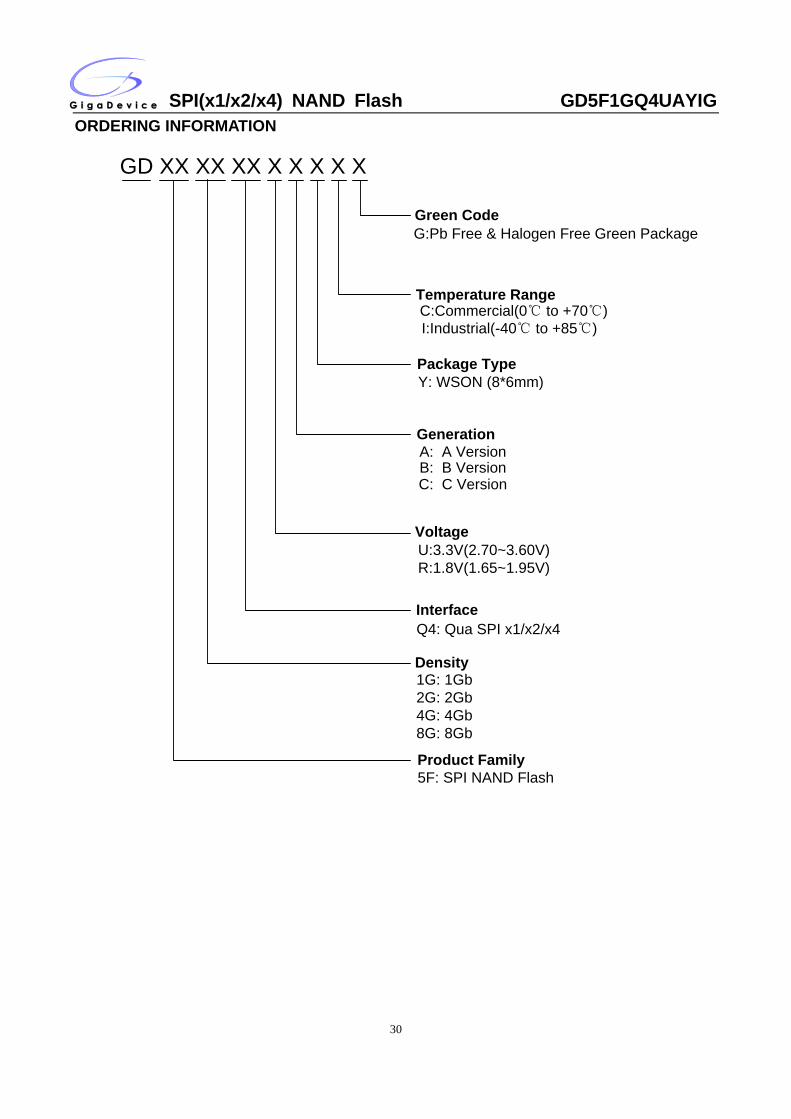
ORDERING INFORMATION
GD XX XX XX X X X X X
Temperature RangeC:Commercial(0℃ to +70℃)I:Industrial(-40℃ to +85℃)
Package TypeY: WSON (8*6mm)
Density
Interface
Product Family5F: SPI NAND Flash
1G: 1Gb2G: 2Gb4G: 4Gb8G: 8Gb
Green Code
GenerationA: A VersionB: B VersionC: C Version
Q4: Qua SPI x1/x2/x4
VoltageU:3.3V(2.70~3.60V)R:1.8V(1.65~1.95V)
G:Pb Free & Halogen Free Green Package
SPI(x1/x2/x4) NAND Flash GD5F1GQ4UAYIG
31
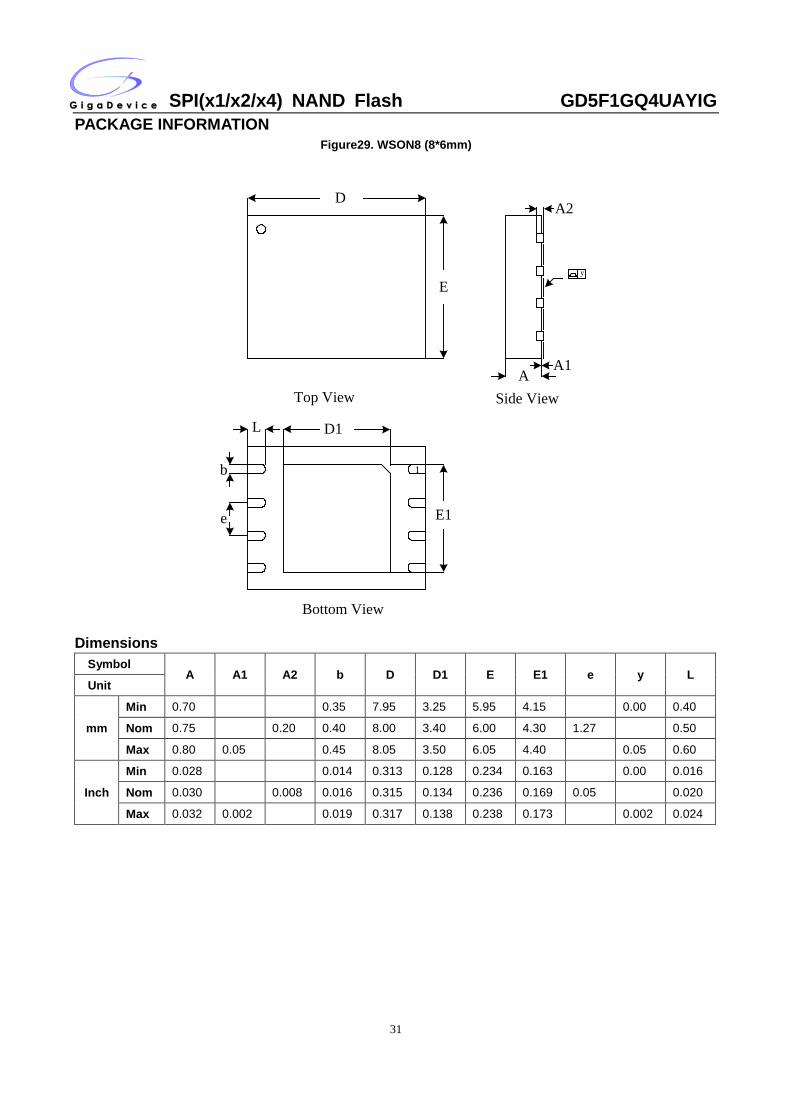
PACKAGE INFORMATION Figure29. WSON8 (8*6mm)
D
E
Top View
D1
E1
b
e
Bottom View
L
1
A2
A1A
Side View
y
Dimensions
Symbol A A1 A2 b D D1 E E1 e y L
Unit
mm
Min 0.70 0.35 7.95 3.25 5.95 4.15 0.00 0.40
Nom 0.75 0.20 0.40 8.00 3.40 6.00 4.30 1.27 0.50
Max 0.80 0.05 0.45 8.05 3.50 6.05 4.40 0.05 0.60
Inch
Min 0.028 0.014 0.313 0.128 0.234 0.163 0.00 0.016
Nom 0.030 0.008 0.016 0.315 0.134 0.236 0.169 0.05 0.020
Max 0.032 0.002 0.019 0.317 0.138 0.238 0.173 0.002 0.024
SPI(x1/x2/x4) NAND Flash GD5F1GQ4UAYIG
32
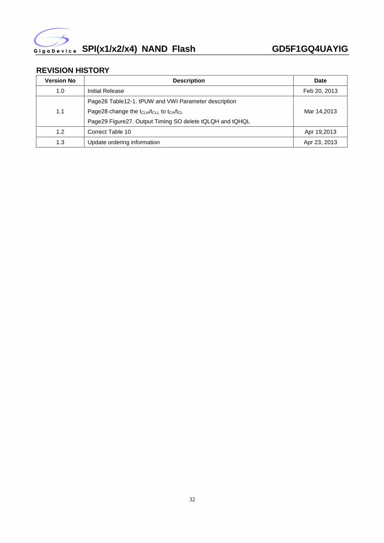
REVISION HISTORY
Version No Description Date
1.0 Initial Release Feb 20, 2013
1.1
Page26 Table12-1. tPUW and VWI Parameter description
Page28 change the tCLH/tCLL to tCH/tCL
Page29 Figure27. Output Timing SO delete tQLQH and tQHQL Mar 14,2013
1.2 Correct Table 10 Apr 19,2013
1.3 Update ordering information Apr 23, 2013