Embed Size (px)
Citation preview
DATE:2006/6/6 1
CUSTOMER
CUSTOMER PART NO.
AMPIRE PART NO. AC-164AYILY-70H
APPROVED BY
DATE
APPROVED BY CHECKED BY ORGANIZED BY
9856 SIXTH STREET RANCHO CUCAMONGA CA 91730 TEL: 909-980-13410 FAX: 909-980-1419
WWW.AMPDISPLAY.COM
AMP DISPLAY INC
AMP DISPLAY INC.
SPECIFICATIONS
DATE:2006/6/6 2
RECORD OF R EVISION
Revision Date Page Contents Editor
2006/6/6
-- New Release
Tony
DATE:2006/6/6 3
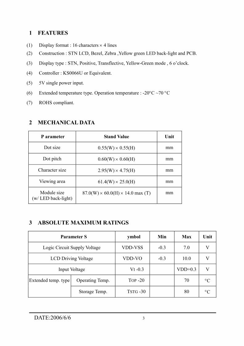
1 FEATURES
(1) Display format : 16 characters × 4 lines (2) Construction : STN LCD, Bezel, Zebra ,Yellow green LED back-light and PCB.
(3) Display type : STN, Positive, Transflective, Yellow-Green mode , 6 o’clock.
(4) Controller : KS0066U or Equivalent.
(5) 5V single power input.
(6) Extended temperature type. Operation temperature : -20°C ~70 °C
(7) ROHS compliant.
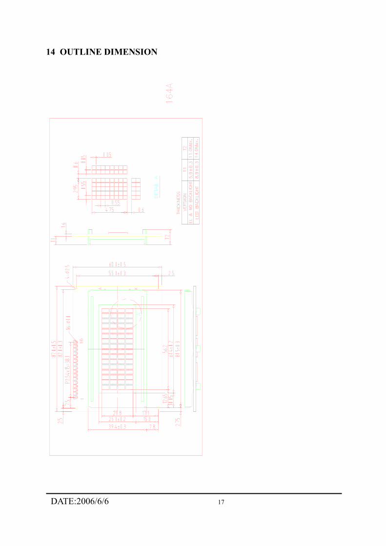
2 MECHANICAL DATA
P arameter Stand Value Unit
Dot size 0.55(W) × 0.55(H) mm
Dot pitch 0.60(W) × 0.60(H) mm
Character size 2.95(W) × 4.75(H) mm
Viewing area 61.4(W) × 25.0(H) mm
Module size (w/ LED back-light)
87.0(W) × 60.0(H) × 14.0 max (T) mm
3 ABSOLUTE MAXIMUM RATINGS
Parameter S ymbol Min Max Unit
Logic Circuit Supply Voltage VDD-VSS -0.3 7.0 V
LCD Driving Voltage VDD-VO -0.3 10.0 V
Input Voltage VI -0.3 VDD+0.3 V
Operating Temp. TOP -20 70 °C Extended temp. type
Storage Temp. TSTG -30 80 °C
DATE:2006/6/6 4
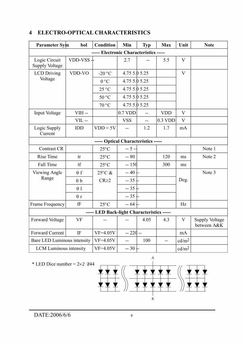
4 ELECTRO-OPTICAL CHARACTERISTICS
Parameter Sym bol Condition Min Typ Max Unit Note ----- Electronic Characteristics -----
Logic Circuit Supply Voltage
VDD-VSS -- 2.7 -- 5.5 V
-20 °C 4.75 5.0 5.25
0 °C 4.75 5.0 5.25
25 °C 4.75 5.0 5.25
50 °C 4.75 5.0 5.25
LCD Driving Voltage
VDD-VO
70 °C 4.75 5.0 5.25
V
VIH -- 0.7 VDD -- VDD V Input Voltage VIL -- VSS -- 0.3 VDD V
Logic Supply Current
IDD VDD = 5V -- 1.2 1.7 mA
----- Optical Characteristics ----- Contrast CR 25°C -- 5 -- Note 1
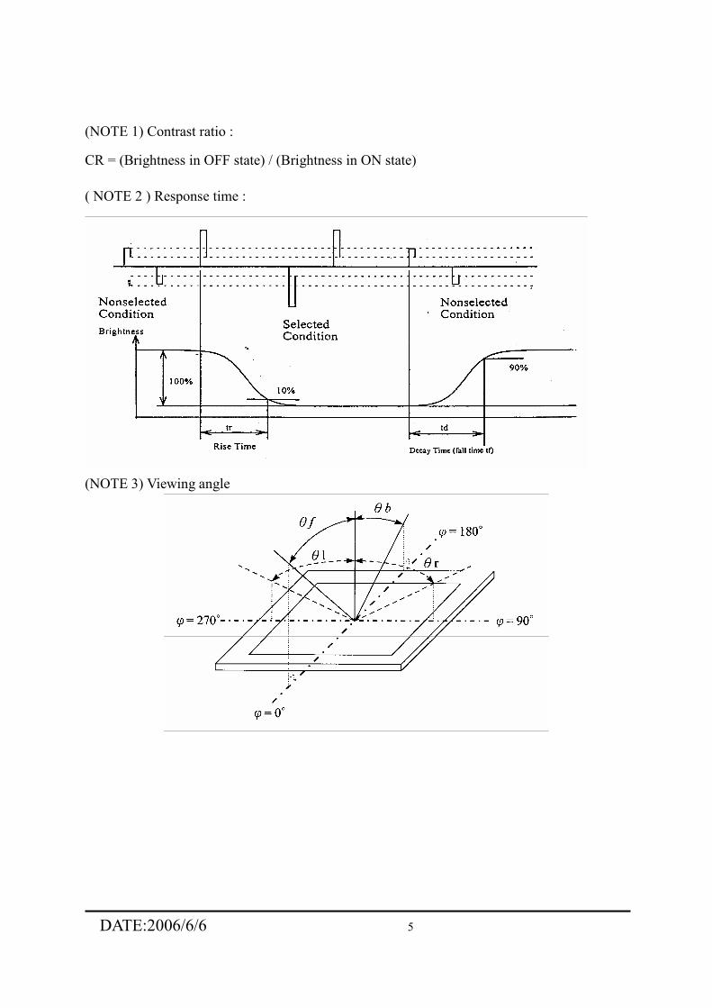
Rise Time tr 25°C -- 80 120 ms Fall Time tf 25°C -- 150 300 ms
Note 2
θ f -- 40 --
θ b -- 35 --
θ l -- 35 --
Viewing Angle Range
θ r
25°C & CR≥2
-- 35 --
Deg.
Note 3
Frame Frequency fF 25°C -- 64 -- Hz ----- LED Back-light Characteristics -----
Forward Voltage VF -- -- 4.05 4.3 V Supply Voltage between A&K
Forward Current IF VF=4.05V -- 220 -- mA Bare LED Luminous intensity VF=4.05V -- 100 -- cd/m2
LCM Luminous intensity VF=4.05V -- 30 -- cd/m2
A
K
* LED Dice number = 2×22=44
DATE:2006/6/6 5
(NOTE 1) Contrast ratio :
CR = (Brightness in OFF state) / (Brightness in ON state)
( NOTE 2 ) Response time :
(NOTE 3) Viewing angle
DATE:2006/6/6 6
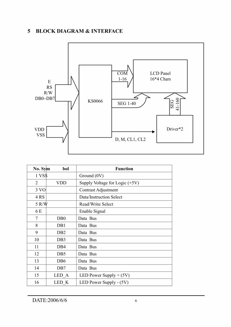
5 BLOCK DIAGRAM & INTERFACE
E
R/WRS
DB0~DB7
VDDVSS
KS0066
LCD Panel16*4 Chars
COM1-16
SEG 1-40
D, M, CL1, CL2
SEG
41-1
60
Driver*2
No. Sym bol Function 1 VSS Ground (0V) 2 VDD Supply Voltage for Logic (+5V) 3 VO Contrast Adjustment 4 RS Data/Instruction Select 5 R/W Read/Write Select 6 E Enable Signal 7 DB0 Data Bus 8 DB1 Data Bus 9 DB2 Data Bus 10 DB3 Data Bus 11 DB4 Data Bus 12 DB5 Data Bus 13 DB6 Data Bus 14 DB7 Data Bus 15 LED_A LED Power Supply + (5V) 16 LED_K LED Power Supply - (5V)
DATE:2006/6/6 7
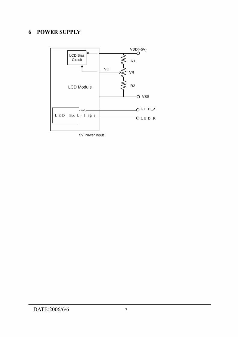
6 POWER SUPPLY
LCD Module
VO
VDD(+5V)
R1
R2
VR
VSS
5V Power Input
LCD BiasCircuit
LED Back-light
LED_A
LED_K
DATE:2006/6/6 8
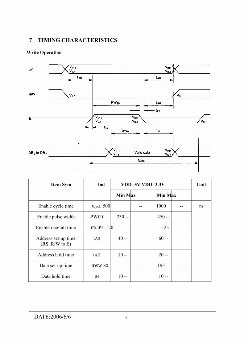
7 TIMING CHARACTERISTICS
Write Operation
VDD=5V VDD=3.3V Item Sym bol
Min Max Min Max
Unit
Enable cycle time tcycE 500 -- 1000 --
Enable pulse width PWEH 230 -- 450 --
Enable rise/fall time tEr,tEf -- 20 -- 25
Address set-up time (RS, R/W to E)
tAS 40 -- 60 --
Address hold time tAH 10 -- 20 --
Data set-up time tDSW 80 -- 195 --
Data hold time tH 10 -- 10 --
ns
DATE:2006/6/6 9
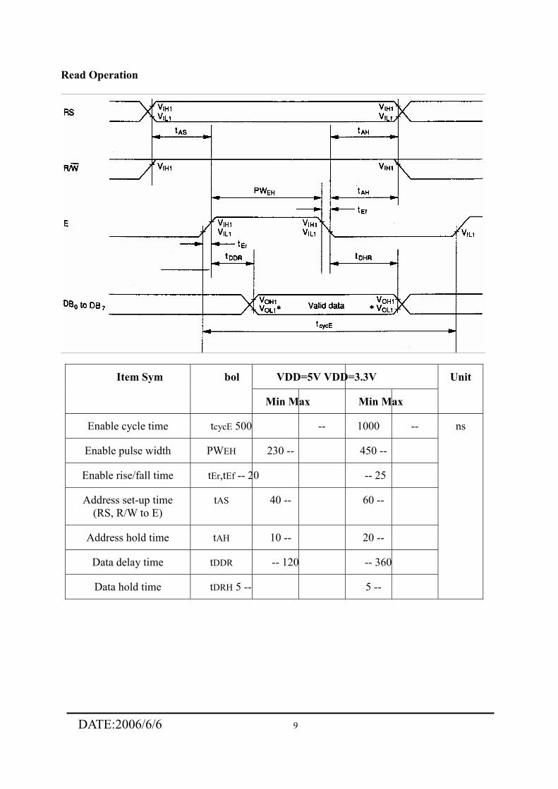
Read Operation
VDD=5V VDD=3.3V Item Sym bol
Min Max Min Max
Unit
Enable cycle time tcycE 500 -- 1000 --
Enable pulse width PWEH 230 -- 450 --
Enable rise/fall time tEr,tEf -- 20 -- 25
Address set-up time (RS, R/W to E)
tAS 40 -- 60 --
Address hold time tAH 10 -- 20 --
Data delay time tDDR -- 120 -- 360
Data hold time tDRH 5 -- 5 --
ns
DATE:2006/6/6 10
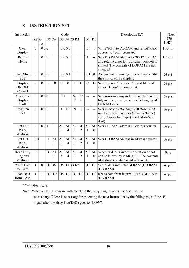
8 INSTRUCTION SET
Code Instruction RS R/
W D7 D6 D5 D4 D3 D2 D1 D0
Description E.T .(fOSC=270 KHZ)
Clear Display
0 0 0 0 0 0 0 0 0 1 Write”20H” to DDRAM and set DDRAM address to “00H” from AC
1.53 ms
Return Home
0 0 0 0 0 0 0 0 1 -- Sets DD RAM address to “00H” from AC and return cursor to its original position if shifted. The contents of DDRAM are not changed.
1.53 ms
Entry Mode SET
0 0 0 0 0 0 0 1 I/D SH Assign cursor moving direction and enable the shift of entire display.
39 µS
Display ON/OFF Control
0 0 0 0 0 0 1 D C B Set display (D), cursor (C), and blink of cursor (B) on/off control bit.
39 µS
Cursor or Display
Shift
0 0 0 0 0 1 S/C
R/L
-- -- Set cursor moving and display shift control bit, and the direction, without changing of DDRAM data.
39 µS
Function Set
0 0 0 0 1 DL N F -- -- Sets interface data length (DL:8-bit/4-bit), number of display lines (N:2-line/1-line) and , display font type (F:5x11dots/5x8 dost).
39 µS
Set CG RAM
Address
0 0 0 1 AC5
AC4
AC3
AC2
AC1
AC0
Sets CG RAM address in address counter. 39 µS
Set DD RAM
Address
0 0 1 AC6
AC5
AC4
AC3
AC2
AC1
AC0
Sets DD RAM address in address counter. 39 µS
Read Busy Flag and Address
0 1 BF AC6
AC5
AC4
AC3
AC2
AC1
AC0
Whether during internal operation or not can be known by reading BF. The contents of address counter can also be read.
0 µS
Write Data to RAM
1 0 D7 D6 D5 D4 D3 D2 D1 D0 Writes data into internal RAM (DD RAM /CG RAM).
43 µS
Read Data from RAM
1 1 D7 D6 D5 D4 D3 D2 D1 D0 Reads data from internal RAM (DD RAM /CG RAM).
43 µS
* “--“ : don’t care Note : When an MPU program with checking the Busy Flag(DB7) is made, it must be
necesssary1/2Fosc is necessary for executing the next instruction by the falling edge of the ‘E’ signal after the Busy Flag(DB7) goes to “LOW”.
DATE:2006/6/6 11
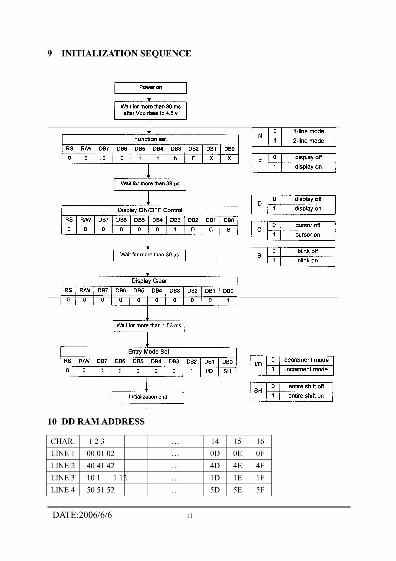
9 INITIALIZATION SEQUENCE
10 DD RAM ADDRESS
CHAR. 1 2 3 … 14 15 16 LINE 1 00 01 02 … 0D 0E 0F LINE 2 40 41 42 … 4D 4E 4F LINE 3 10 1 1 12 … 1D 1E 1F LINE 4 50 51 52 … 5D 5E 5F
DATE:2006/6/6 12
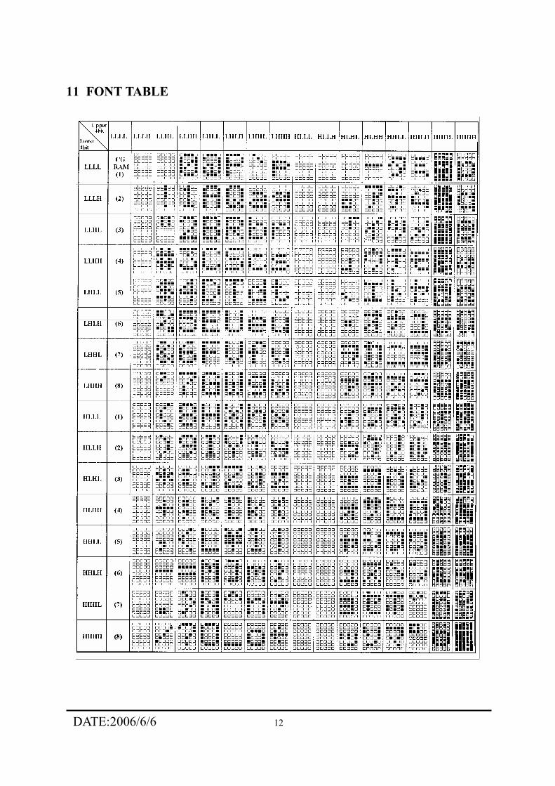
11 FONT TABLE
DATE:2006/6/6 13
12 QUALITY AND RELIABILITY
12.1 TEST CONDITIONS
T ests should be conducted under the following conditions : Ambie nt temperature : 25 ± 5°C Humidity : 60 ± 25% RH.
12.2 SAMPLING PLAN
Sampling method shall be in accordance with M IL-STD-105E , l evel II, norm al single sampling plan .
12.3 ACCEPTABLE QUALITY LEVEL
A major defect is defined as one that could cause failure to or materially reduce the
usability of the unit f or i ts intended purpose. A minor defect is one tha t does not ma terially reduce the usability of the unit for its intended purpose or is an infringement from established standards and has no significant bearing on its effective use or operation.
12.4 APPEARANCE
An appearance test should be conducted by human sight at approximately 30 cm distance from the LCD module under flourescent light. The inspection area of LCD panel shall be within the range of following limits.
DATE:2006/6/6 14
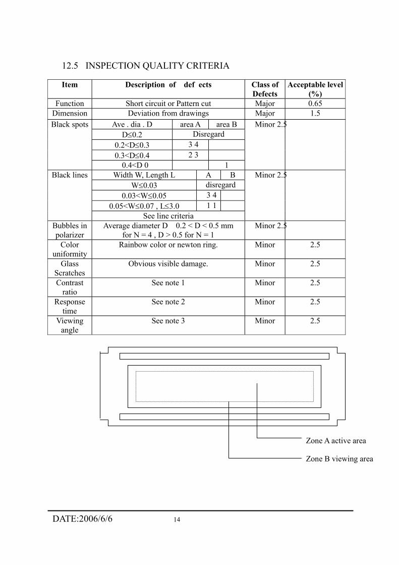
12.5 INSPECTION QUALITY CRITERIA
Item Description of def ects Class of Defects
Acceptable level (%)
Function Short circuit or Pattern cut Major 0.65 Dimension Deviation from drawings Major 1.5
Ave . dia . D area A area B D≤0.2 Disregard
0.2<D≤0.3 3 4 0.3<D≤0.4 2 3
Black spots
0.4<D 0 1
Minor 2.5
Width W, Length L A B W≤0.03 disregard
0.03<W≤0.05 3 4 0.05<W≤0.07 , L≤3.0 1 1
Black lines
See line criteria
Minor 2.5
Bubbles in polarizer
Average diameter D 0.2 < D < 0.5 mm for N = 4 , D > 0.5 for N = 1
Minor 2.5
Color uniformity
Rainbow color or newton ring. Minor 2.5
Glass Scratches
Obvious visible damage. Minor 2.5
Contrast ratio
See note 1 Minor 2.5
Response time
See note 2 Minor 2.5
Viewing angle
See note 3 Minor 2.5
Zone A active area
Zone B viewing area
DATE:2006/6/6 15
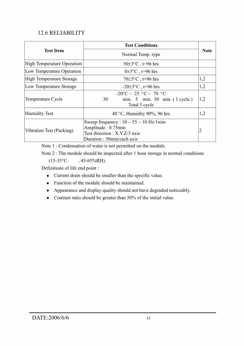
12.6 RELIABILITY
Test Conditions Test Item
Normal Temp. type Note
High Temperature Operation 50±3°C , t=96 hrs Low Temperature Operation 0±3°C , t=96 hrs High Temperature Storage 70±3°C , t=96 hrs 1,2 Low Temperature Storage -20±3°C , t=96 hrs 1,2
Temperature Cycle -20°C ~ 25 °C ~ 70 °C
30 min. 5 min. 30 min. ( 1 cycle ) Total 5 cycle
1,2
Humidity Test 40 °C, Humidity 90%, 96 hrs 1,2
Vibration Test (Packing)
Sweep frequency : 10 ~ 55 ~ 10 Hz/1min Amplitude : 0.75mm Test direction : X.Y.Z/3 axis Duration : 30min/each axis
2
Note 1 : Condensation of water is not permitted on the module. Note 2 : The module should be inspected after 1 hour storage in normal conditions (15-35°C , 45-65%RH). Definitions of life end point :
Current drain should be smaller than the specific value. Function of the module should be maintained. Appearance and display quality should not have degraded noticeably. Contrast ratio should be greater than 50% of the initial value.
DATE:2006/6/6 16
13 HANDLING PRECAUTIONS
(1) A LCD module is a fragile item and should not be subjected to strong mechanical shocks.
(2) Avoid applying pressure to the module surface. This will distort the glass and cause a change in color.
(3) Under no circumstances should the position of the bezel tabs or their shape be modified.
(4) Do not modify the display PCB in either shape or positioning of components.
(5) Do not modify or move location of the zebra or heat seal connectors.
(6) The device should only be soldered to during interfacing. Modification to other areas of the board should not be carried out.
(7) In the event of LCD breakage and resultant leakage of fluid do not inhale, ingest or make contact with the skin. If contact is made rinse immediately.
(8) When cleaning the module use a soft damp cloth with a mild solvent, such as Isopropyl or Ethyl alcohol. The use of water, ketone or aromatic is not permitted.
(9) Prior to initial power up input signals should not be applied.
(10) Protect the module against static electricity and observe appropriate anti-static precautions.
DATE:2006/6/6 17
14 OUTLINE DIMENSION