Embed Size (px)
Citation preview
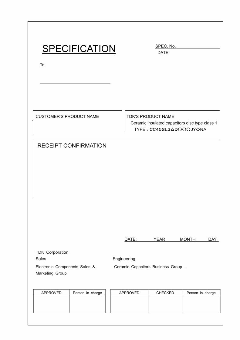
SPEC No.
SPECIFICATION To
CUSTOMER’S PRODUCT NAME TDK’S PRODUCT NAME
Ceramic insulated capacitors disc type class 1
TYPE:CC45SL3DJYNA
RECEIPT CONFIRMATION
DATE: YEAR MONTH DAY
TDK Corporation Sales Engineering
Electronic Components Sales &
Marketing Group
Ceramic Capacitors Business Group .
APPROVED Person in charge APPROVED CHECKED Person in charge
SPEC. No.
DATE:
SPEC No.
Handling precautions for High voltage ceramic capacitors Please read the following closely before using these products.
Safety precautions The following precautions should be observed strictly to ensure safety design.
Misuse of the product may lead to smoking of the product.
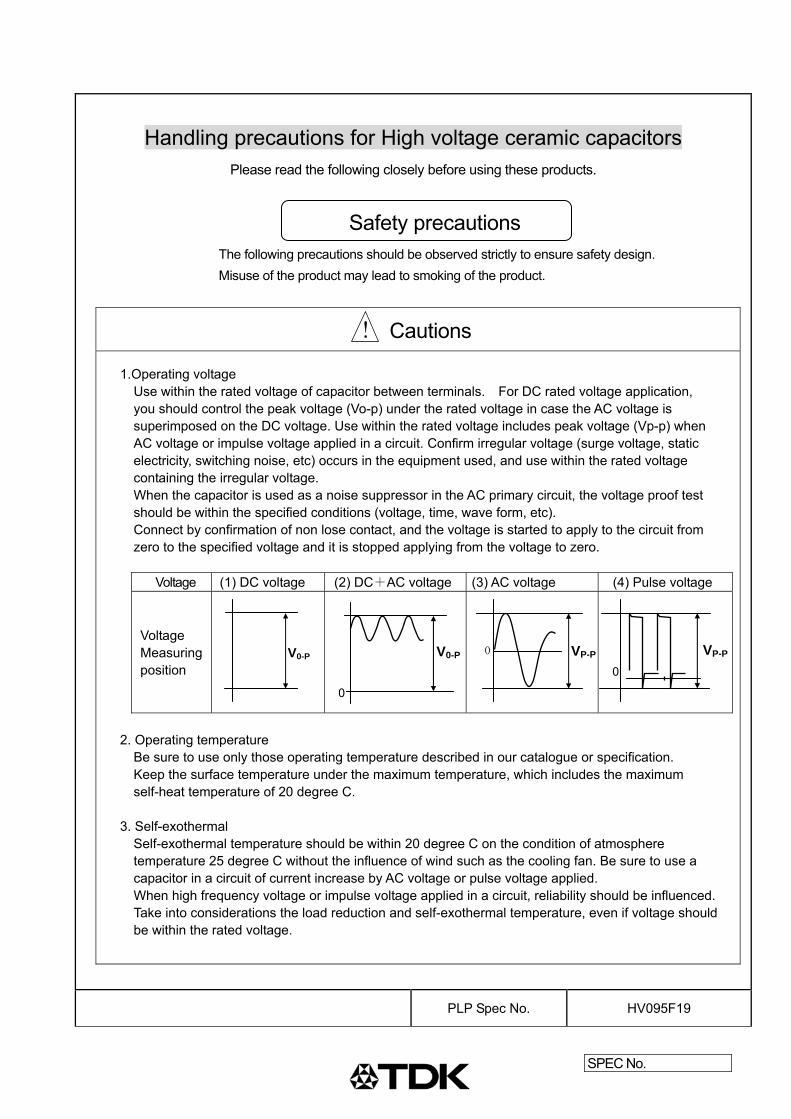
! Cautions 1.Operating voltage
Use within the rated voltage of capacitor between terminals. For DC rated voltage application, you should control the peak voltage (Vo-p) under the rated voltage in case the AC voltage is superimposed on the DC voltage. Use within the rated voltage includes peak voltage (Vp-p) when AC voltage or impulse voltage applied in a circuit. Confirm irregular voltage (surge voltage, static electricity, switching noise, etc) occurs in the equipment used, and use within the rated voltage containing the irregular voltage. When the capacitor is used as a noise suppressor in the AC primary circuit, the voltage proof test should be within the specified conditions (voltage, time, wave form, etc). Connect by confirmation of non lose contact, and the voltage is started to apply to the circuit from zero to the specified voltage and it is stopped applying from the voltage to zero.
Voltage (1) DC voltage (2) DC+AC voltage (3) AC voltage (4) Pulse voltage
Voltage Measuring position
V0-P
2. Operating temperature
Be sure to use only those operating temperature described in our catalogue or specification. Keep the surface temperature under the maximum temperature, which includes the maximum self-heat temperature of 20 degree C.
3. Self-exothermal
Self-exothermal temperature should be within 20 degree C on the condition of atmosphere temperature 25 degree C without the influence of wind such as the cooling fan. Be sure to use a capacitor in a circuit of current increase by AC voltage or pulse voltage applied. When high frequency voltage or impulse voltage applied in a circuit, reliability should be influenced. Take into considerations the load reduction and self-exothermal temperature, even if voltage should be within the rated voltage.
PLP Spec No. HV095F19
V0-P
0
0 VP-P
0
VP-P
SPEC No.
! Cautions
4. Capacitance change of capacitors
For some of the capacitors, capacitance value may change considerably in the temperature range, or by applied DC voltage. And capacitor has aging characteristic (capacitance decreases by keeping as it is).When you use the capacitor in the time constant circuit, consult TDK whether the capacitor is available or not.
5. Vibration of capacitors
When the capacitor class 2 is used in the AC circuit, or pulse circuit, the capacitor might vibrate or noise might occur in the specified frequency. Be sure to confirm the conditions before using the capacitor.
6. Usage of capacitance and storage
Don’t use capacitors in the following environments: * Direct sunshine * Areas directly exposed to water or salty water * Areas that become dewy * Areas filled with toxic gases (such as hydrogen sulfide, sulfur dioxide, chlorine, ammonia, etc) * Areas exposed to excess vibrations or shock conditions described in our catalogue or specification. Store capacitors in an environment from -10 to 40 degree C, with 15 to 70%RH for 6 months maximum
and use within the period after receiving the capacitors. 7. Inserting precautions
When inserting capacitors into the PC board by automatic insertion machine, confirm the conditions (such as pressure of pusher, adjustment of clinching portion) and minimize the impact force by chucking the body, or clinching the lead terminals. Distances between the hole position onto a PC board should be equal to the pitch of capacitors.
When stretching the lead terminal, any force may load the bottom of the capacitor body and result in damage to the insulation coating. Severe damages may cause poor reliability.
8. Soldering
Don’t immerse the capacitor body into the molten solder, and don’t solder the terminals by reflow soldering. Use PC board, and solder the terminals in the opposite side of the body. Soldering conditions, such as pre-heat temperature, soldering temperature, and soldering time, should be followed by the descriptions in our catalogue or specification. (refer to Fig.-1) Adjust the amount of solder within the proper volume. Select an appropriate soldering material. When using soldering iron for installing capacitors or reworking onto the PC board, sufficient pre-heating and temperature control should be used. We recommend that the iron condition is 350±10 degree C/ 3.5±0.5s. as 1 time, and you should use an adequate tip diameter (φ3mm Max.) with the soldering iron as well as a proper wattage (50W Max.). Don’t touch the capacitor body directly with soldering tip, except for the terminals of capacitor.
9. Flux
When using flux for soldering capacitors onto the PC board, spread it thinly and uniformly. Flux will be composed of halogenated material less than 0.1 wt% (cl conversion). Don’t use a strong acid grade of flux. When using water-soluble flux, sufficient cleansing should be done.
PLP Spec No. HV095F19
SPEC No.
! Cautions
10. Cleansing
When the cleansing should not be sufficient, the cleansing liquid or any residue might leave on the capacitor body, they may deteriorate the insulation coating or performance (insulation resistance, etc.). When using ultrasonic cleansing, avoid transmitting vibrations onto the PC board. Conditions of ultrasonic cleansing, such as output frequency and time of the method, should be taken into considerations. After cleansing capacitors, dry them well. Cleansing liquid should not contain electrolyte, nor leave any residue. Through the result of the cleansing method, confirm whether the quality of the capacitors have been affected due to the conditions.
11. Coating or molding
When coating or molding capacitors after installing components onto the PC board, confirm whether the performance of capacitors may not be damaged by the work.
12. Mechanical stress
Don’t submit to excessive mechanical shock. Don’t use capacitors which may have been damaged dueto dropping, etc. If possible, avoid bending the terminals of capacitors. In an unavoidable case of bending, use a small jig to decrease the mechanical stress on the capacitors.
13. Others
Please contact TDK before using our capacitors listed in this catalogue or specifications for the applications listed below which require especially high reliability for the prevention of defects which might directly cause damage to the third party’s life, body or property, or when intending to use one of our capacitors for other applications than specified in this catalog or specifications. * Medical equipment * Aerospace equipment * Power plant equipment * Aircraft equipment * Transportation equipment (vehicles, trains, ships, etc) * Undersea equipment * Traffic signal equipment * Disaster prevention, crime prevention equipment * Data processing equipment exerting influence on public * Application of similar complexity and, or reliability requirements to the applications listed in the above.
Please refer to the guideline of notabilia for fixed ceramic capacitors issued by JEITA (Japan Electronics and Information Technology Association, EIAJ RCR-2335).
PLP Spec No. HV095F19
SPEC No.
Scope This specification applies to ceramic insulated capacitors disc type used in electronic equipment.
Relative standards
JIS C 6423-1991
JIS C 5102-1994
Mention item
1. Part No.
2. Operating temperature range
3. Test condition
4. Performance
5. Marking
6. Figure & Dimension
7. Label, Packing & Transport
8. Notification before the modification
We do not use the following material (1),(2) in these products.
(1) PBBOs (Poly Bromo Biphenyl Oxides)
(2) PBBs (Poly Bromo Biphenyls)
We do not use Class ⅠODS (Ozone depleting substances ) in all our process of these products.
These products shall conform to RoHS Directive
These products are Halogen-free.(Br≦900ppm, Cl≦900ppm, Br+Cl≦1500ppm) Manufacturing place
Manufacturing site should be TDK Taiwan & TDK Xiamen
Divisio Date Issued SPEC. No.
Ceramic Capacitors Business Group
-1-
SPEC No.
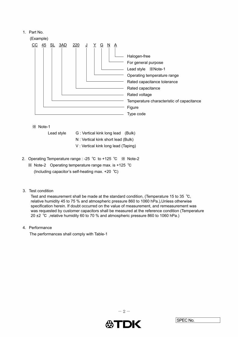
1.Part No.
(Example)
CC 45 SL 3AD 220 J Y G N A
Halogen-free
For general purpose
Lead style ※Note-1
Operating temperature range
Rated capacitance tolerance
Rated capacitance
Rated voltage
Temperature characteristic of capacitance
Figure
Type code
※ Note-1
Lead style G : Vertical kink long lead (Bulk)
N : Vertical kink short lead (Bulk)
V : Vertical kink long lead (Taping)
2.Operating Temperature range : -25 to +125 ※ Note-2
※ Note-2 Operating temperature range max. is +125
(Including capacitor’s self-heating max. +20 )
3.Test condition Test and measurement shall be made at the standard condition, (Temperature 15 to 35 , relative humidity 45 to 75 % and atmospheric pressure 860 to 1060 hPa.),Unless otherwise specification herein. If doubt occurred on the value of measurement, and remeasurement was was requested by customer capacitors shall be measured at the reference condition (Temperature 20 ±2 ,relative humidity 60 to 70 % and atmospheric pressure 860 to 1060 hPa.)
4.Performance
The performances shall comply with Table-1
-2-
SPEC No.
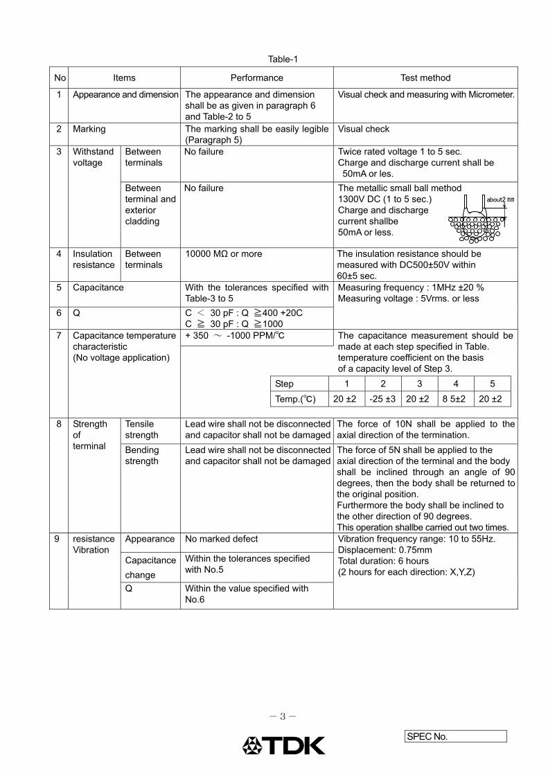
Table-1
No Items Performance Test method
1 Appearance and dimension The appearance and dimension shall be as given in paragraph 6 and Table-2 to 5
Visual check and measuring with Micrometer.
2 Marking The marking shall be easily legible (Paragraph 5)
Visual check
3 Withstand voltage
Between terminals
No failure Twice rated voltage 1 to 5 sec. Charge and discharge current shall be 50mA or les.
Between terminal and exterior cladding
No failure The metallic small ball method 1300V DC (1 to 5 sec.) Charge and discharge current shallbe 50mA or less.
4 Insulation resistance
Between terminals
10000 MΩ or more The insulation resistance should be measured with DC500±50V within 60±5 sec.
5 Capacitance With the tolerances specified with Table-3 to 5
Measuring frequency : 1MHz ±20 % Measuring voltage : 5Vrms. or less 6 Q C < 30 pF : Q ≧400 +20C
C ≧ 30 pF : Q ≧1000 7
Capacitance temperature characteristic (No voltage application)
+ 350 ~ -1000 PPM/ The capacitance measurement should be made at each step specified in Table. temperature coefficient on the basis of a capacity level of Step 3.
8 Strength of terminal
Tensile strength
Lead wire shall not be disconnectedand capacitor shall not be damaged
The force of 10N shall be applied to the axial direction of the termination.
Bending strength
Lead wire shall not be disconnectedand capacitor shall not be damaged
The force of 5N shall be applied to the axial direction of the terminal and the bodyshall be inclined through an angle of 90 degrees, then the body shall be returned to the original position. Furthermore the body shall be inclined to the other direction of 90 degrees. This operation shallbe carried out two times.
9 resistance Vibration
Appearance No marked defect Vibration frequency range: 10 to 55Hz. Displacement: 0.75mm Total duration: 6 hours (2 hours for each direction: X,Y,Z)
Capacitance
change
Within the tolerances specified with No.5
Q Within the value specified with No.6
-3-
about2
Step 1 2 3 4 5
Temp.() 20 ±2 -25 ±3 20 ±2 8 5±2 20 ±2
SPEC No.
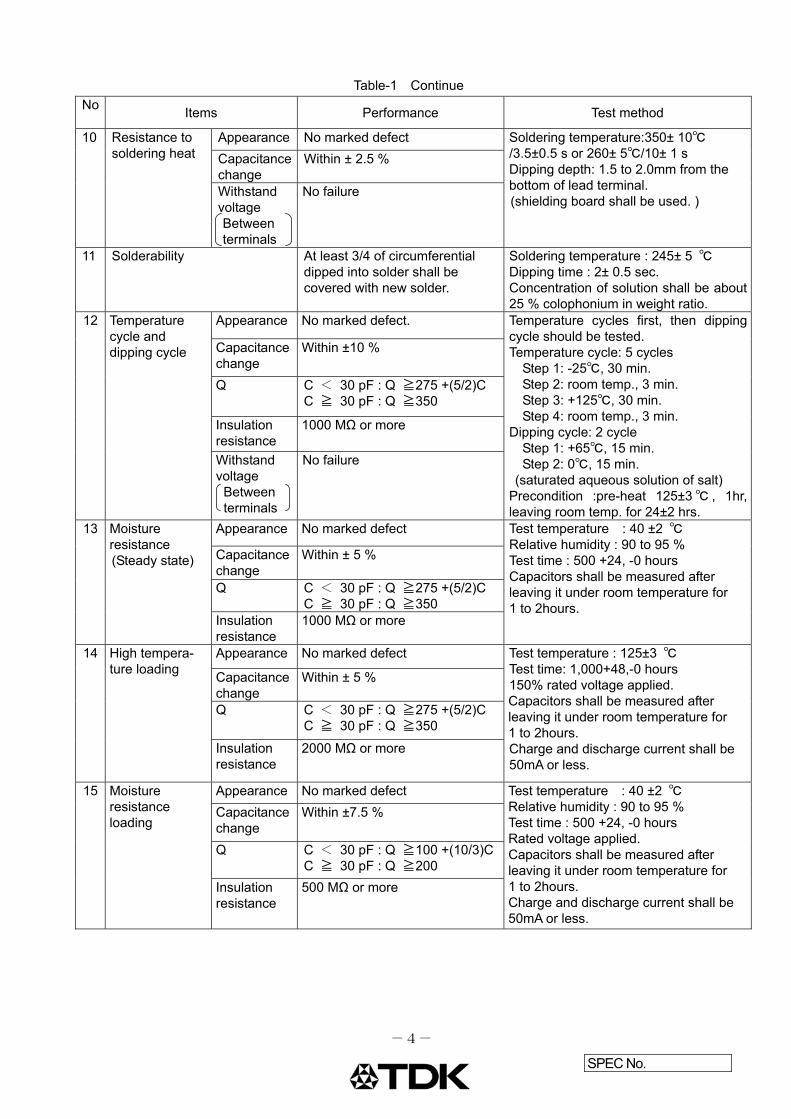
Table-1 Continue
No Items Performance Test method
10 Resistance to soldering heat
Appearance No marked defect Soldering temperature:350± 10 /3.5±0.5 s or 260± 5/10± 1 s Dipping depth: 1.5 to 2.0mm from the bottom of lead terminal. (shielding board shall be used. )
Capacitance change
Within ± 2.5 %
Withstand voltage Between terminals
No failure
11 Solderability At least 3/4 of circumferential dipped into solder shall be covered with new solder.
Soldering temperature : 245± 5 Dipping time : 2± 0.5 sec. Concentration of solution shall be about 25 % colophonium in weight ratio.
12 Temperature cycle and dipping cycle
Appearance No marked defect. Temperature cycles first, then dipping cycle should be tested. Temperature cycle: 5 cycles
Step 1: -25, 30 min. Step 2: room temp., 3 min. Step 3: +125, 30 min. Step 4: room temp., 3 min.
Dipping cycle: 2 cycle Step 1: +65, 15 min. Step 2: 0, 15 min.
(saturated aqueous solution of salt) Precondition :pre-heat 125±3 , 1hr, leaving room temp. for 24±2 hrs.
Capacitance change
Within ±10 %
Q C < 30 pF : Q ≧275 +(5/2)C C ≧ 30 pF : Q ≧350
Insulation resistance
1000 MΩ or more
Withstand voltage
Between terminals
No failure
13 Moisture resistance (Steady state)
Appearance No marked defect Test temperature : 40 ±2 Relative humidity : 90 to 95 % Test time : 500 +24, -0 hours Capacitors shall be measured after leaving it under room temperature for 1 to 2hours.
Capacitance change
Within ± 5 %
Q C < 30 pF : Q ≧275 +(5/2)C C ≧ 30 pF : Q ≧350
Insulation resistance
1000 MΩ or more
14 High tempera- ture loading
Appearance No marked defect Test temperature : 125±3 Test time: 1,000+48,-0 hours 150% rated voltage applied. Capacitors shall be measured after leaving it under room temperature for 1 to 2hours. Charge and discharge current shall be 50mA or less.
Capacitance change
Within ± 5 %
Q C < 30 pF : Q ≧275 +(5/2)C C ≧ 30 pF : Q ≧350
Insulation resistance
2000 MΩ or more
15 Moisture resistance loading
Appearance No marked defect Test temperature : 40 ±2 Relative humidity : 90 to 95 % Test time : 500 +24, -0 hours Rated voltage applied. Capacitors shall be measured after leaving it under room temperature for 1 to 2hours. Charge and discharge current shall be 50mA or less.
Capacitance change
Within ±7.5 %
Q C < 30 pF : Q ≧100 +(10/3)CC ≧ 30 pF : Q ≧200
Insulation resistance
500 MΩ or more
-4-
SPEC No.
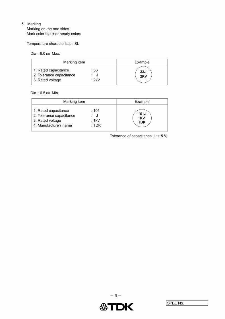
5.Marking Marking on the one sides Mark color black or nearly colors Temperature characteristic : SL
Dia:6.0 Max.
Dia:6.5 Min.
Tolerance of capacitance J : ± 5 %
Marking item Example
1. Rated capacitance : 33 2. Tolerance capacitance : J 3. Rated voltage : 2kV
Marking item Example
1. Rated capacitance : 101 2. Tolerance capacitance : J 3. Rated voltage : 1kV 4. Manufacture’s name : TDK
33J 2KV
101J1KV TDK
-5-
SPEC No.
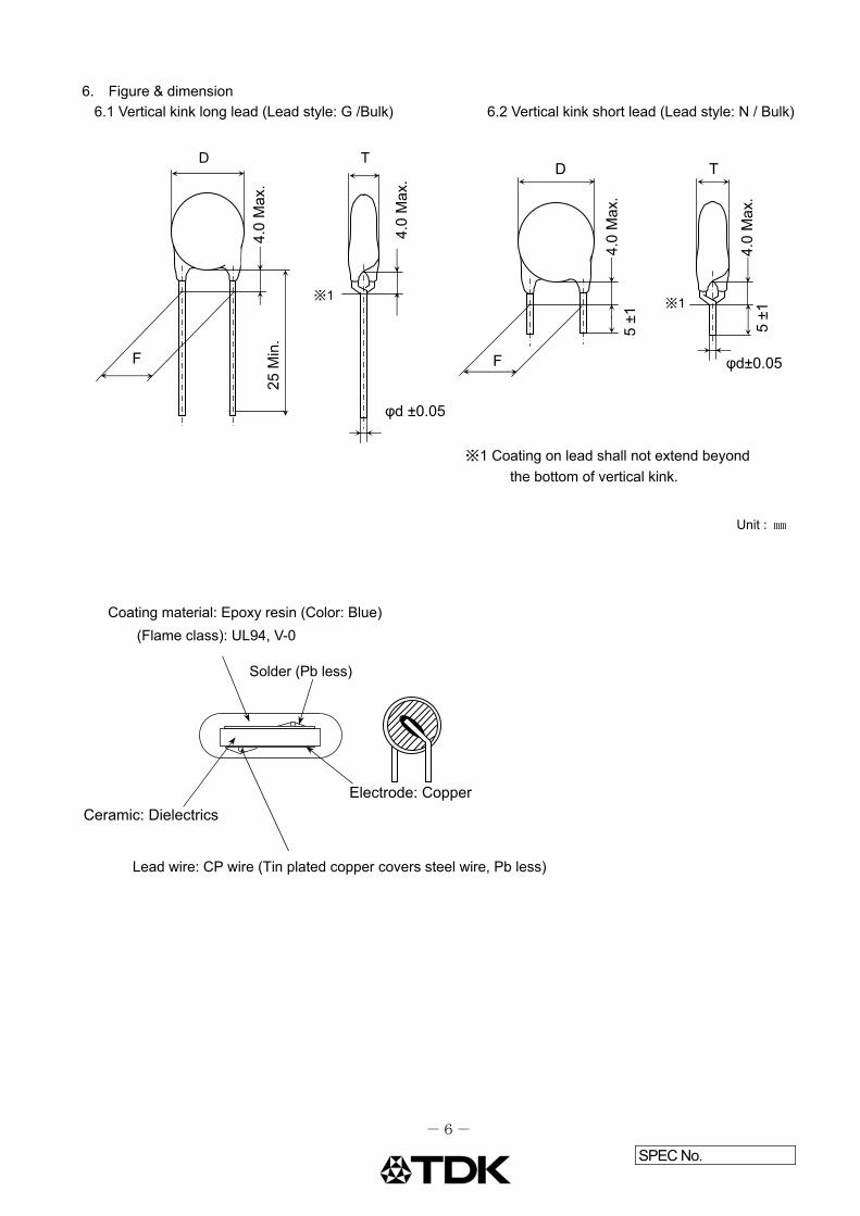
6. Figure & dimension
6.1 Vertical kink long lead (Lead style: G /Bulk) 6.2 Vertical kink short lead (Lead style: N / Bulk)
D T
※1 Coating on lead shall not extend beyond
the bottom of vertical kink.
Coating material: Epoxy resin (Color: Blue)
(Flame class): UL94, V-0
Lead wire: CP wire (Tin plated copper covers steel wire, Pb less)
5 ±1
4.0
Max
.
4.0
Max
.
25 M
in.
φd ±0.05
※1
5 ±1
φd±0.05
※1
4.0
Max
.
4.0
Max
.
F
D T
Unit :
-6-
F
Solder (Pb less)
Electrode: Copper
Ceramic: Dielectrics

SPEC No.
6.3 Vertical kink long lead (lead style: V / Taping)
(F=5.0mm, Pitch: 12.7mm, Shape: A, at Table-3~5)
Table-2 Unit : mm
Item Symbol Dimension Remarks
Name
Body diameter D Table-3~5
Body thickness T Table-3~5
Lead-wire diameter φd 0.6 ±0.05
Pitch of component P 12.7 ±1.0 Including the slant of body
Feed hole pitch P0 12.7 ±0.3 Excepting the tape splicing part
Feed hole center to lead P1 3.85 ±0.7
Feed hole center to component P2 6.35 ±1.3 Including the slanting body due to bending lead-wire
Lead-to lead distanc F 5.0 +0.8,-0.2 Measuring point is bottom kink
Component alignment, F-R h 0 ± 2.0 Including the slanting body due to bending lead-wire
Tape width W 18.0 +1.0,-0.5
Adhesive tape width W0 10.0 Min.
Hole position W1 9.0 ±0.5
Adhesive tape position W2 4.0 Max. Adhesive tape do not stick out the tape
Bottom of kink from tape center H0 16.0 +1.5,-0.5
Height of body from tape center H1 46.0 Max.
Lead-wire protrusion ℓ 1.0 Max.
Feed hole diameter D0 4.0 ±0.2
Total tape thickness t 0.6 ±0.3 Including adhesive tape
Length of snipped lead L 11.0 Max.
Coating on lead C 4.0 Max.
Height of kink A 4.0 Max. Measuring point is bottom of kink
Spring action S 2.0 Max.
∆h
φd
T D
S F P
P P2
D0
∆h
P0
H1
L W
H0
t
A
W2 C
W W
0
H0
-7-
ℓ ℓ
SPEC No.
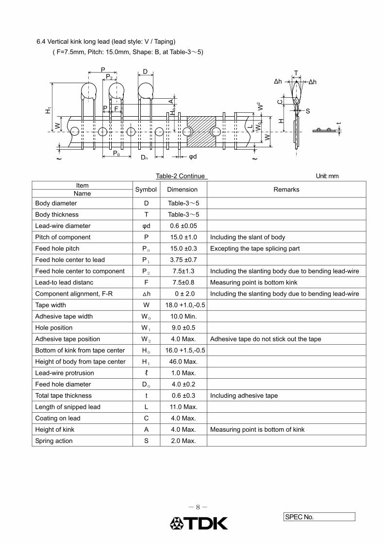
6.4 Vertical kink long lead (lead style: V / Taping)
( F=7.5mm, Pitch: 15.0mm, Shape: B, at Table-3~5)
Table-2 Continue Unit: mm
Item Symbol Dimension Remarks
Name
Body diameter D Table-3~5
Body thickness T Table-3~5
Lead-wire diameter φd 0.6 ±0.05
Pitch of component P 15.0 ±1.0 Including the slant of body
Feed hole pitch P0 15.0 ±0.3 Excepting the tape splicing part
Feed hole center to lead P1 3.75 ±0.7
Feed hole center to component P2 7.5±1.3 Including the slanting body due to bending lead-wire
Lead-to lead distanc F 7.5±0.8 Measuring point is bottom kink
Component alignment, F-R h 0 ± 2.0 Including the slanting body due to bending lead-wire
Tape width W 18.0 +1.0,-0.5
Adhesive tape width W0 10.0 Min.
Hole position W1 9.0 ±0.5
Adhesive tape position W2 4.0 Max. Adhesive tape do not stick out the tape
Bottom of kink from tape center H0 16.0 +1.5,-0.5
Height of body from tape center H1 46.0 Max.
Lead-wire protrusion ℓ 1.0 Max.
Feed hole diameter D0 4.0 ±0.2
Total tape thickness t 0.6 ±0.3 Including adhesive tape
Length of snipped lead L 11.0 Max.
Coating on lead C 4.0 Max.
Height of kink A 4.0 Max. Measuring point is bottom of kink
Spring action S 2.0 Max.
∆h
φd
T D
S F P
P P2
D0
∆h
P0
H1
L W
H t
A
W2 C
W W
0
H0
-8-
ℓ ℓ
SPEC No.
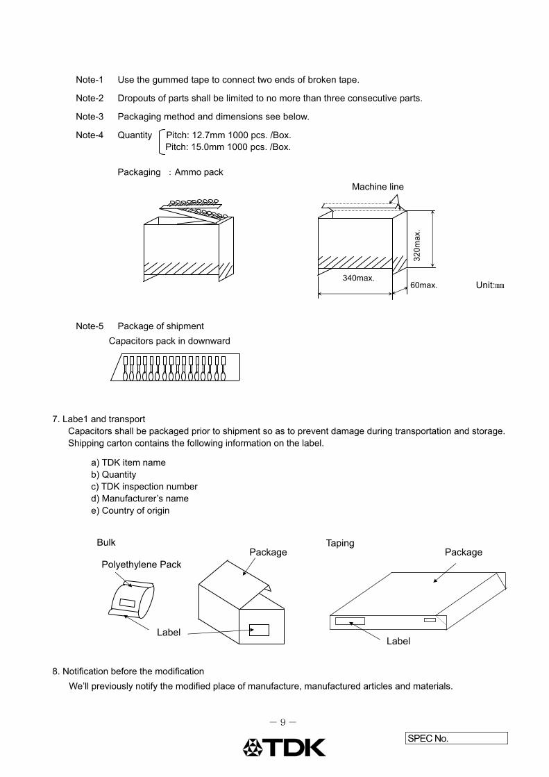
Note-1 Use the gummed tape to connect two ends of broken tape.
Note-2 Dropouts of parts shall be limited to no more than three consecutive parts.
Note-3 Packaging method and dimensions see below.
Note-4 Quantity Pitch: 12.7mm 1000 pcs. /Box. Pitch: 15.0mm 1000 pcs. /Box.
Packaging :Ammo pack
Machine line
Unit:
Note-5 Package of shipment
Capacitors pack in downward
7. Labe1 and transport Capacitors shall be packaged prior to shipment so as to prevent damage during transportation and storage. Shipping carton contains the following information on the label.
a) TDK item name b) Quantity c) TDK inspection number d) Manufacturer’s name e) Country of origin
8. Notification before the modification
We’ll previously notify the modified place of manufacture, manufactured articles and materials.
-9-
60max.
320m
ax.
340max.
Polyethylene Pack
Package
Label
Bulk Taping Package
Label
SPEC No.
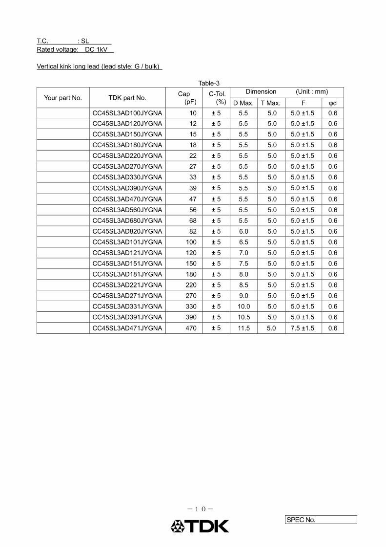
T.C. : SL Rated voltage: DC 1kV Vertical kink long lead (lead style: G / bulk)
Table-3
Your part No. TDK part No. Cap
(pF)C-Tol.
(%)
Dimension (Unit : mm)
D Max. T Max. F φd
CC45SL3AD100JYGNA 10 ± 5 5.5 5.0 5.0 ±1.5 0.6
CC45SL3AD120JYGNA 12 ± 5 5.5 5.0 5.0 ±1.5 0.6
CC45SL3AD150JYGNA 15 ± 5 5.5 5.0 5.0 ±1.5 0.6
CC45SL3AD180JYGNA 18 ± 5 5.5 5.0 5.0 ±1.5 0.6
CC45SL3AD220JYGNA 22 ± 5 5.5 5.0 5.0 ±1.5 0.6
CC45SL3AD270JYGNA 27 ± 5 5.5 5.0 5.0 ±1.5 0.6
CC45SL3AD330JYGNA 33 ± 5 5.5 5.0 5.0 ±1.5 0.6
CC45SL3AD390JYGNA 39 ± 5 5.5 5.0 5.0 ±1.5 0.6
CC45SL3AD470JYGNA 47 ± 5 5.5 5.0 5.0 ±1.5 0.6
CC45SL3AD560JYGNA 56 ± 5 5.5 5.0 5.0 ±1.5 0.6
CC45SL3AD680JYGNA 68 ± 5 5.5 5.0 5.0 ±1.5 0.6
CC45SL3AD820JYGNA 82 ± 5 6.0 5.0 5.0 ±1.5 0.6
CC45SL3AD101JYGNA 100 ± 5 6.5 5.0 5.0 ±1.5 0.6
CC45SL3AD121JYGNA 120 ± 5 7.0 5.0 5.0 ±1.5 0.6
CC45SL3AD151JYGNA 150 ± 5 7.5 5.0 5.0 ±1.5 0.6
CC45SL3AD181JYGNA 180 ± 5 8.0 5.0 5.0 ±1.5 0.6
CC45SL3AD221JYGNA 220 ± 5 8.5 5.0 5.0 ±1.5 0.6
CC45SL3AD271JYGNA 270 ± 5 9.0 5.0 5.0 ±1.5 0.6
CC45SL3AD331JYGNA 330 ± 5 10.0 5.0 5.0 ±1.5 0.6
CC45SL3AD391JYGNA 390 ± 5 10.5 5.0 5.0 ±1.5 0.6
CC45SL3AD471JYGNA 470 ± 5 11.5 5.0 7.5 ±1.5 0.6
-10-

SPEC No.
T.C. : SL Rated voltage: DC 1kV Vertical kink short lead (lead style: N / bulk)
Table-3 Continue
Your part No. TDK part No. Cap.
(pF)C-Tol. (%)
Dimension (Unit : mm)
D Max. T Max. F φd
CC45SL3AD100JYNNA 10 ± 5 5.5 5.0 5.0 ±1.5 0.6
CC45SL3AD120JYNNA 12 ± 5 5.5 5.0 5.0 ±1.5 0.6
CC45SL3AD150JYNNA 15 ± 5 5.5 5.0 5.0 ±1.5 0.6
CC45SL3AD180JYNNA 18 ± 5 5.5 5.0 5.0 ±1.5 0.6
CC45SL3AD220JYNNA 22 ± 5 5.5 5.0 5.0 ±1.5 0.6
CC45SL3AD270JYNNA 27 ± 5 5.5 5.0 5.0 ±1.5 0.6
CC45SL3AD330JYNNA 33 ± 5 5.5 5.0 5.0 ±1.5 0.6
CC45SL3AD390JYNNA 39 ± 5 5.5 5.0 5.0 ±1.5 0.6
CC45SL3AD470JYNNA 47 ± 5 5.5 5.0 5.0 ±1.5 0.6
CC45SL3AD560JYNNA 56 ± 5 5.5 5.0 5.0 ±1.5 0.6
CC45SL3AD680JYNNA 68 ± 5 5.5 5.0 5.0 ±1.5 0.6
CC45SL3AD820JYNNA 82 ± 5 6.0 5.0 5.0 ±1.5 0.6
CC45SL3AD101JYNNA 100 ± 5 6.5 5.0 5.0 ±1.5 0.6
CC45SL3AD121JYNNA 120 ± 5 7.0 5.0 5.0 ±1.5 0.6
CC45SL3AD151JYNNA 150 ± 5 7.5 5.0 5.0 ±1.5 0.6
CC45SL3AD181JYNNA 180 ± 5 8.0 5.0 5.0 ±1.5 0.6
CC45SL3AD221JYNNA 220 ± 5 8.5 5.0 5.0 ±1.5 0.6
CC45SL3AD271JYNNA 270 ± 5 9.0 5.0 5.0 ±1.5 0.6
CC45SL3AD331JYNNA 330 ± 5 10.0 5.0 5.0 ±1.5 0.6
CC45SL3AD391JYNNA 390 ± 5 10.5 5.0 5.0 ±1.5 0.6
CC45SL3AD471JYNNA 470 ± 5 11.5 5.0 7.5 ±1.5 0.6
-11-
SPEC No.
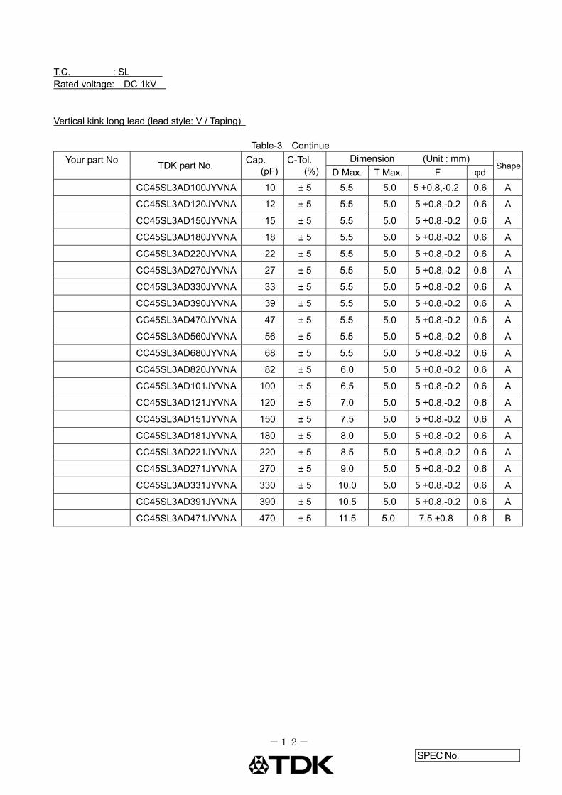
T.C. : SL Rated voltage: DC 1kV Vertical kink long lead (lead style: V / Taping)
Table-3 Continue
Your part No
TDK part No. Cap.
(pF)C-Tol.
(%)Dimension (Unit : mm)
ShapeD Max. T Max. F φd
CC45SL3AD100JYVNA 10 ± 5 5.5 5.0 5 +0.8,-0.2 0.6 A
CC45SL3AD120JYVNA 12 ± 5 5.5 5.0 5 +0.8,-0.2 0.6 A
CC45SL3AD150JYVNA 15 ± 5 5.5 5.0 5 +0.8,-0.2 0.6 A
CC45SL3AD180JYVNA 18 ± 5 5.5 5.0 5 +0.8,-0.2 0.6 A
CC45SL3AD220JYVNA 22 ± 5 5.5 5.0 5 +0.8,-0.2 0.6 A
CC45SL3AD270JYVNA 27 ± 5 5.5 5.0 5 +0.8,-0.2 0.6 A
CC45SL3AD330JYVNA 33 ± 5 5.5 5.0 5 +0.8,-0.2 0.6 A
CC45SL3AD390JYVNA 39 ± 5 5.5 5.0 5 +0.8,-0.2 0.6 A
CC45SL3AD470JYVNA 47 ± 5 5.5 5.0 5 +0.8,-0.2 0.6 A
CC45SL3AD560JYVNA 56 ± 5 5.5 5.0 5 +0.8,-0.2 0.6 A
CC45SL3AD680JYVNA 68 ± 5 5.5 5.0 5 +0.8,-0.2 0.6 A
CC45SL3AD820JYVNA 82 ± 5 6.0 5.0 5 +0.8,-0.2 0.6 A
CC45SL3AD101JYVNA 100 ± 5 6.5 5.0 5 +0.8,-0.2 0.6 A
CC45SL3AD121JYVNA 120 ± 5 7.0 5.0 5 +0.8,-0.2 0.6 A
CC45SL3AD151JYVNA 150 ± 5 7.5 5.0 5 +0.8,-0.2 0.6 A
CC45SL3AD181JYVNA 180 ± 5 8.0 5.0 5 +0.8,-0.2 0.6 A
CC45SL3AD221JYVNA 220 ± 5 8.5 5.0 5 +0.8,-0.2 0.6 A
CC45SL3AD271JYVNA 270 ± 5 9.0 5.0 5 +0.8,-0.2 0.6 A
CC45SL3AD331JYVNA 330 ± 5 10.0 5.0 5 +0.8,-0.2 0.6 A
CC45SL3AD391JYVNA 390 ± 5 10.5 5.0 5 +0.8,-0.2 0.6 A
CC45SL3AD471JYVNA 470 ± 5 11.5 5.0 7.5 ±0.8 0.6 B
-12-
SPEC No.
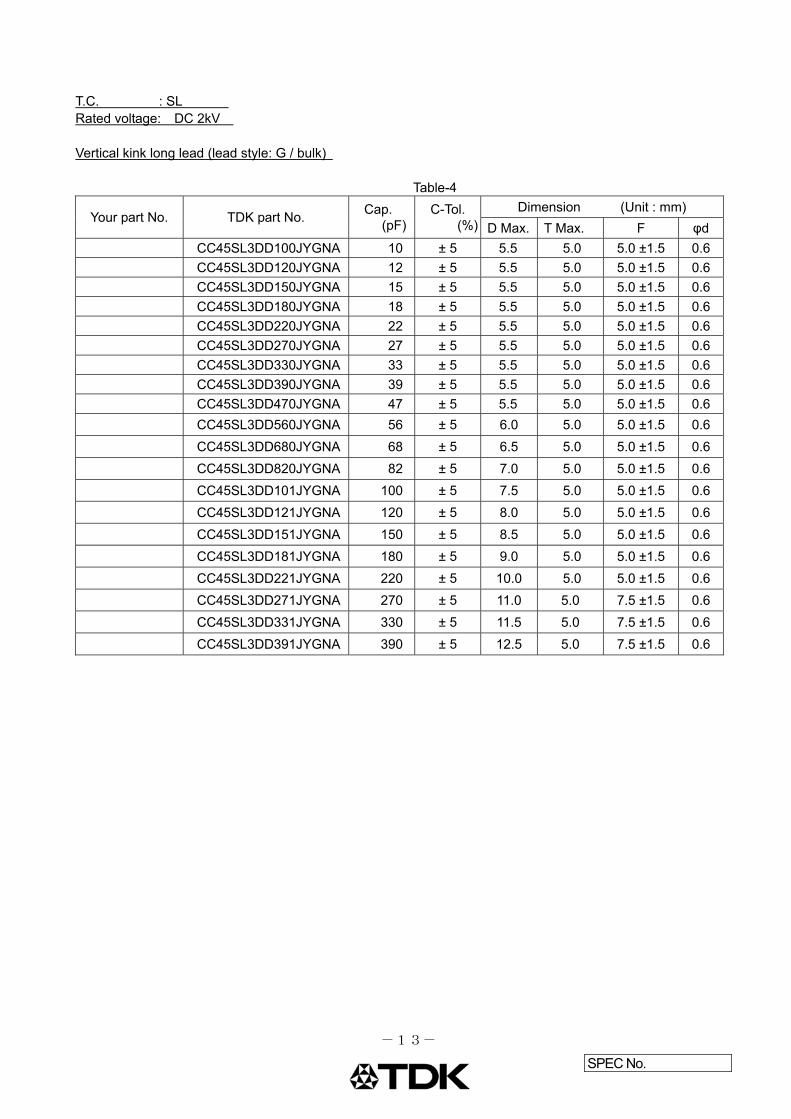
T.C. : SL Rated voltage: DC 2kV Vertical kink long lead (lead style: G / bulk)
Table-4
Your part No. TDK part No. Cap.
(pF)C-Tol.
(%)Dimension (Unit : mm)
D Max. T Max. F φd
CC45SL3DD100JYGNA 10 ± 5 5.5 5.0 5.0 ±1.5 0.6
CC45SL3DD120JYGNA 12 ± 5 5.5 5.0 5.0 ±1.5 0.6
CC45SL3DD150JYGNA 15 ± 5 5.5 5.0 5.0 ±1.5 0.6
CC45SL3DD180JYGNA 18 ± 5 5.5 5.0 5.0 ±1.5 0.6
CC45SL3DD220JYGNA 22 ± 5 5.5 5.0 5.0 ±1.5 0.6
CC45SL3DD270JYGNA 27 ± 5 5.5 5.0 5.0 ±1.5 0.6
CC45SL3DD330JYGNA 33 ± 5 5.5 5.0 5.0 ±1.5 0.6
CC45SL3DD390JYGNA 39 ± 5 5.5 5.0 5.0 ±1.5 0.6
CC45SL3DD470JYGNA 47 ± 5 5.5 5.0 5.0 ±1.5 0.6
CC45SL3DD560JYGNA 56 ± 5 6.0 5.0 5.0 ±1.5 0.6
CC45SL3DD680JYGNA 68 ± 5 6.5 5.0 5.0 ±1.5 0.6
CC45SL3DD820JYGNA 82 ± 5 7.0 5.0 5.0 ±1.5 0.6
CC45SL3DD101JYGNA 100 ± 5 7.5 5.0 5.0 ±1.5 0.6
CC45SL3DD121JYGNA 120 ± 5 8.0 5.0 5.0 ±1.5 0.6
CC45SL3DD151JYGNA 150 ± 5 8.5 5.0 5.0 ±1.5 0.6
CC45SL3DD181JYGNA 180 ± 5 9.0 5.0 5.0 ±1.5 0.6
CC45SL3DD221JYGNA 220 ± 5 10.0 5.0 5.0 ±1.5 0.6
CC45SL3DD271JYGNA 270 ± 5 11.0 5.0 7.5 ±1.5 0.6
CC45SL3DD331JYGNA 330 ± 5 11.5 5.0 7.5 ±1.5 0.6
CC45SL3DD391JYGNA 390 ± 5 12.5 5.0 7.5 ±1.5 0.6
-13-

SPEC No.
T.C. : SL Rated voltage: DC 2kV Vertical kink short lead (lead style: N / bulk)
Table-4 Continue
Your part No. TDK part No. Cap.
(pF)C-Tol. (%)
Dimension (Unit : mm)
D Max. T Max. F φd
CC45SL3DD100JYNNA 10 ± 5 5.5 5.0 5.0 ±1.5 0.6
CC45SL3DD120JYNNA 12 ± 5 5.5 5.0 5.0 ±1.5 0.6
CC45SL3DD150JYNNA 15 ± 5 5.5 5.0 5.0 ±1.5 0.6
CC45SL3DD180JYNNA 18 ± 5 5.5 5.0 5.0 ±1.5 0.6
CC45SL3DD220JYNNA 22 ± 5 5.5 5.0 5.0 ±1.5 0.6
CC45SL3DD270JYNNA 27 ± 5 5.5 5.0 5.0 ±1.5 0.6
CC45SL3DD330JYNNA 33 ± 5 5.5 5.0 5.0 ±1.5 0.6
CC45SL3DD390JYNNA 39 ± 5 5.5 5.0 5.0 ±1.5 0.6
CC45SL3DD470JYNNA 47 ± 5 5.5 5.0 5.0 ±1.5 0.6
CC45SL3DD560JYNNA 56 ± 5 6.0 5.0 5.0 ±1.5 0.6
CC45SL3DD680JYNNA 68 ± 5 6.5 5.0 5.0 ±1.5 0.6
CC45SL3DD820JYNNA 82 ± 5 7.0 5.0 5.0 ±1.5 0.6
CC45SL3DD101JYNNA 100 ± 5 7.5 5.0 5.0 ±1.5 0.6
CC45SL3DD121JYNNA 120 ± 5 8.0 5.0 5.0 ±1.5 0.6
CC45SL3DD151JYNNA 150 ± 5 8.5 5.0 5.0 ±1.5 0.6
CC45SL3DD181JYNNA 180 ± 5 9.0 5.0 5.0 ±1.5 0.6
CC45SL3DD221JYNNA 220 ± 5 10.0 5.0 5.0 ±1.5 0.6
CC45SL3DD271JYNNA 270 ± 5 11.0 5.0 7.5 ±1.5 0.6
CC45SL3DD331JYNNA 330 ± 5 11.5 5.0 7.5 ±1.5 0.6
CC45SL3DD391JYNNA 390 ± 5 12.5 5.0 7.5 ±1.5 0.6
-14-

SPEC No.
T.C. : SL Rated voltage: DC 2kV Vertical kink long lead (lead style: V / Taping)
Table-4 Continue
Your part No. TDK part No. Cap.
(pF)C-Tol.
(%)
Dimension (Unit : mm) Shape
D Max. T Max. F φd
CC45SL3DD100JYVNA 10 ± 5 5.5 5.0 5 +0.8,-02 0.6 A
CC45SL3DD120JYVNA 12 ± 5 5.5 5.0 5 +0.8,-02 0.6 A
CC45SL3DD150JYVNA 15 ± 5 5.5 5.0 5 +0.8,-02 0.6 A
CC45SL3DD180JYVNA 18 ± 5 5.5 5.0 5 +0.8,-02 0.6 A
CC45SL3DD220JYVNA 22 ± 5 5.5 5.0 5 +0.8,-02 0.6 A
CC45SL3DD270JYVNA 27 ± 5 5.5 5.0 5 +0.8,-02 0.6 A
CC45SL3DD330JYVNA 33 ± 5 5.5 5.0 5 +0.8,-02 0.6 A
CC45SL3DD390JYVNA 39 ± 5 5.5 5.0 5 +0.8,-02 0.6 A
CC45SL3DD470JYVNA 47 ± 5 5.5 5.0 5 +0.8,-02 0.6 A
CC45SL3DD560JYVNA 56 ± 5 6.0 5.0 5 +0.8,-02 0.6 A
CC45SL3DD680JYVNA 68 ± 5 6.5 5.0 5 +0.8,-02 0.6 A
CC45SL3DD820JYVNA 82 ± 5 7.0 5.0 5 +0.8,-02 0.6 A
CC45SL3DD101JYVNA 100 ± 5 7.5 5.0 5 +0.8,-02 0.6 A
CC45SL3DD121JYVNA 120 ± 5 8.0 5.0 5 +0.8,-02 0.6 A
CC45SL3DD151JYVNA 150 ± 5 8.5 5.0 5 +0.8,-02 0.6 A
CC45SL3DD181JYVNA 180 ± 5 9.0 5.0 5 +0.8,-02 0.6 A
CC45SL3DD221JYVNA 220 ± 5 10.0 5.0 5 +0.8,-02 0.6 A
CC45SL3DD271JYVNA 270 ± 5 11.0 5.0 7.5 ±0.8 0.6 B
CC45SL3DD331JYVNA 330 ± 5 11.5 5.0 7.5 ±0.8 0.6 B
CC45SL3DD391JYVNA 390 ± 5 12.5 5.0 7.5 ±0.8 0.6 B
-15-
SPEC No.
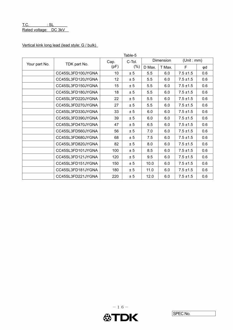
T.C. : SL Rated voltage: DC 3kV Vertical kink long lead (lead style: G / bulk)
Table-5
Your part No. TDK part No. Cap.
(pF)C-Tol. (%)
Dimension (Unit : mm)
D Max. T Max. F φd
CC45SL3FD100JYGNA 10 ± 5 5.5 6.0 7.5 ±1.5 0.6
CC45SL3FD120JYGNA 12 ± 5 5.5 6.0 7.5 ±1.5 0.6
CC45SL3FD150JYGNA 15 ± 5 5.5 6.0 7.5 ±1.5 0.6
CC45SL3FD180JYGNA 18 ± 5 5.5 6.0 7.5 ±1.5 0.6
CC45SL3FD220JYGNA 22 ± 5 5.5 6.0 7.5 ±1.5 0.6
CC45SL3FD270JYGNA 27 ± 5 5.5 6.0 7.5 ±1.5 0.6
CC45SL3FD330JYGNA 33 ± 5 6.0 6.0 7.5 ±1.5 0.6
CC45SL3FD390JYGNA 39 ± 5 6.0 6.0 7.5 ±1.5 0.6
CC45SL3FD470JYGNA 47 ± 5 6.5 6.0 7.5 ±1.5 0.6
CC45SL3FD560JYGNA 56 ± 5 7.0 6.0 7.5 ±1.5 0.6
CC45SL3FD680JYGNA 68 ± 5 7.5 6.0 7.5 ±1.5 0.6
CC45SL3FD820JYGNA 82 ± 5 8.0 6.0 7.5 ±1.5 0.6
CC45SL3FD101JYGNA 100 ± 5 8.5 6.0 7.5 ±1.5 0.6
CC45SL3FD121JYGNA 120 ± 5 9.5 6.0 7.5 ±1.5 0.6
CC45SL3FD151JYGNA 150 ± 5 10.0 6.0 7.5 ±1.5 0.6
CC45SL3FD181JYGNA 180 ± 5 11.0 6.0 7.5 ±1.5 0.6
CC45SL3FD221JYGNA 220 ± 5 12.0 6.0 7.5 ±1.5 0.6
-16-
SPEC No.
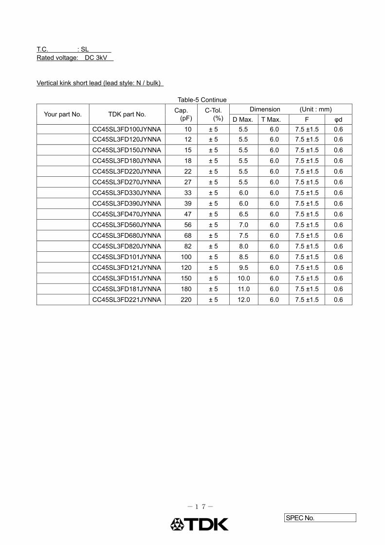
T.C. : SL Rated voltage: DC 3kV Vertical kink short lead (lead style: N / bulk)
Table-5 Continue
Your part No. TDK part No. Cap.
(pF)C-Tol. (%)
Dimension (Unit : mm)
D Max. T Max. F φd
CC45SL3FD100JYNNA 10 ± 5 5.5 6.0 7.5 ±1.5 0.6
CC45SL3FD120JYNNA 12 ± 5 5.5 6.0 7.5 ±1.5 0.6
CC45SL3FD150JYNNA 15 ± 5 5.5 6.0 7.5 ±1.5 0.6
CC45SL3FD180JYNNA 18 ± 5 5.5 6.0 7.5 ±1.5 0.6
CC45SL3FD220JYNNA 22 ± 5 5.5 6.0 7.5 ±1.5 0.6
CC45SL3FD270JYNNA 27 ± 5 5.5 6.0 7.5 ±1.5 0.6
CC45SL3FD330JYNNA 33 ± 5 6.0 6.0 7.5 ±1.5 0.6
CC45SL3FD390JYNNA 39 ± 5 6.0 6.0 7.5 ±1.5 0.6
CC45SL3FD470JYNNA 47 ± 5 6.5 6.0 7.5 ±1.5 0.6
CC45SL3FD560JYNNA 56 ± 5 7.0 6.0 7.5 ±1.5 0.6
CC45SL3FD680JYNNA 68 ± 5 7.5 6.0 7.5 ±1.5 0.6
CC45SL3FD820JYNNA 82 ± 5 8.0 6.0 7.5 ±1.5 0.6
CC45SL3FD101JYNNA 100 ± 5 8.5 6.0 7.5 ±1.5 0.6
CC45SL3FD121JYNNA 120 ± 5 9.5 6.0 7.5 ±1.5 0.6
CC45SL3FD151JYNNA 150 ± 5 10.0 6.0 7.5 ±1.5 0.6
CC45SL3FD181JYNNA 180 ± 5 11.0 6.0 7.5 ±1.5 0.6
CC45SL3FD221JYNNA 220 ± 5 12.0 6.0 7.5 ±1.5 0.6
-17-
SPEC No.
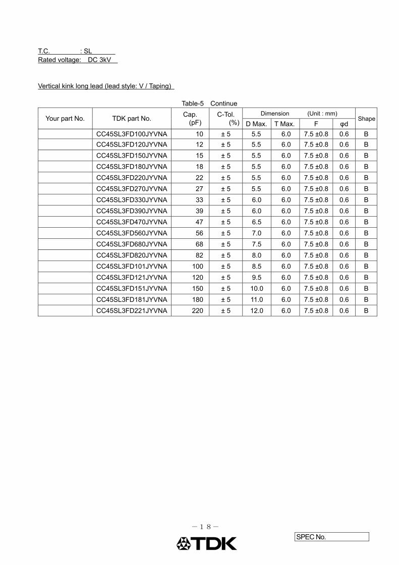
T.C. : SL Rated voltage: DC 3kV Vertical kink long lead (lead style: V / Taping)
Table-5 Continue
Your part No. TDK part No. Cap.
(pF) C-Tol. (%)
Dimension (Unit : mm) Shape
D Max. T Max. F φd
CC45SL3FD100JYVNA 10 ± 5 5.5 6.0 7.5 ±0.8 0.6 B
CC45SL3FD120JYVNA 12 ± 5 5.5 6.0 7.5 ±0.8 0.6 B
CC45SL3FD150JYVNA 15 ± 5 5.5 6.0 7.5 ±0.8 0.6 B
CC45SL3FD180JYVNA 18 ± 5 5.5 6.0 7.5 ±0.8 0.6 B
CC45SL3FD220JYVNA 22 ± 5 5.5 6.0 7.5 ±0.8 0.6 B
CC45SL3FD270JYVNA 27 ± 5 5.5 6.0 7.5 ±0.8 0.6 B
CC45SL3FD330JYVNA 33 ± 5 6.0 6.0 7.5 ±0.8 0.6 B
CC45SL3FD390JYVNA 39 ± 5 6.0 6.0 7.5 ±0.8 0.6 B
CC45SL3FD470JYVNA 47 ± 5 6.5 6.0 7.5 ±0.8 0.6 B
CC45SL3FD560JYVNA 56 ± 5 7.0 6.0 7.5 ±0.8 0.6 B
CC45SL3FD680JYVNA 68 ± 5 7.5 6.0 7.5 ±0.8 0.6 B
CC45SL3FD820JYVNA 82 ± 5 8.0 6.0 7.5 ±0.8 0.6 B
CC45SL3FD101JYVNA 100 ± 5 8.5 6.0 7.5 ±0.8 0.6 B
CC45SL3FD121JYVNA 120 ± 5 9.5 6.0 7.5 ±0.8 0.6 B
CC45SL3FD151JYVNA 150 ± 5 10.0 6.0 7.5 ±0.8 0.6 B
CC45SL3FD181JYVNA 180 ± 5 11.0 6.0 7.5 ±0.8 0.6 B
CC45SL3FD221JYVNA 220 ± 5 12.0 6.0 7.5 ±0.8 0.6 B
-18-
SPEC No.
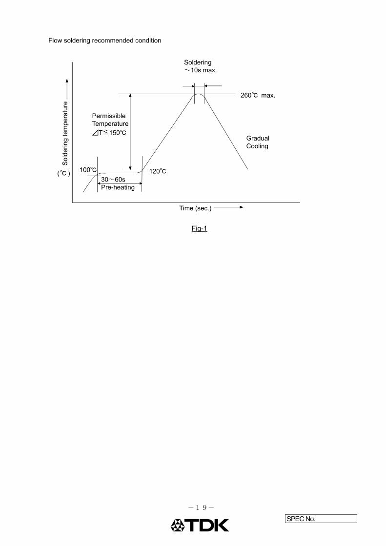
Flow soldering recommended condition
Fig-1
Time (sec.)
260 max.
100 120 ( )
Permissible Temperature
⊿T≦150
Soldering ~10s max.
Gradual Cooling
30~60s Pre-heating
Sol
derin
g te
mpe
ratu
re
-19-