Embed Size (px)
Citation preview

SPECIFICATION
To
Non-Controlled Copy
CUSTOMER’S PRODUCT NAME TDK’S PRODUCT NAMEMultilayer ceramic capacitorsDipped radial lead typeFK-SeriesGeneral (Up to 50V)Mid voltage (100 to 630V)
RECEIPT CONFIRMATION
DATE: YEAR MONTH DAY
TDK CorporationSales
Electronic Components Sales &Marketing Group
Engineering
TDK-EPC CORPORATIONCeramic Capacitors Business Group
TDK-MCC CORPORATIONDIELECTRIC PRODUCTS ENGINEERING DEPT.
APPROVED Person in charge APPROVED CHECKED Person in charge
SPEC. No. D2013-C9DATE: 2013 Sep.

―― 1 ――
1. SCOPEThis specification is applicable to multilayer ceramic capacitors dipped radial lead type
with a priority over the other relevant specifications.
Production places defined in this specification shall be TDK Xiamen Co., Ltd. (China).
EXPLANATORY NOTE:
This specification warrants the quality of the lead type ceramic capacitor. The parts
should be evaluated or confirmed a state of used on your product.
If the use of the parts go beyond the bounds of the specification, we can not afford to
guarantee.
2. CODE CONSTRUCTION(Example) FK28 X7R 1H 104 K N006
(1) (2) (3) (4) (5) (6)
(1)Type
Dimensions (Unit : mm)Type
L(max.) W(max.) T(max.) F φd
FK18 4.0 5.5 2.5
FK14 4.5 5.5 2.5
FK16 5.5 6.0 3.5
FK11 5.5 7.0 4.0
2.5±0.8 5.0+3.0
-1.00.5
+0.10
-0.03
*FK denotes forming lead.
The first digit refers to a distance between leads ( 1-2.5mm ),
the second digit is for TDK internal code.
*Dimension is applied to bulk packaging.
Refer to Appendix 2 for dimension of taping packaging.
F
φd
L
W
T
FK14
TL
F
φd
W
FK18
F
φd
L
W
T
FK16F
φd
L
W
T
FK11

―― 2 ――
(1)Type
Dimensions (Unit : mm)Type
L(max.) W(max.) T(max.) F φd
FK28 4.0 5.5 2.5
FK24 4.5 5.5 2.5
FK26 5.5 6.0 3.5
FK20 5.5 7.0 4.0
FK22 7.5 8.0 4.0
5.0±1.0 7.0±2.0 0.5+0.10
-0.03
*FK denotes forming lead.
The first digit refers to a distance between leads ( 2-5.0mm ),
the second digit is for TDK internal code.
*Dimension is applied to bulk packaging.
Refer to Appendix 3 for dimension of taping packaging.
(2)Temperature Characteristics (Details are shown in para 7 No.7,8)
φd
F
L
W
T
FK20
φd
TL
W
F
FK26
φd
F
L
T
W
FK22
F
L
W
T
φd
FK28
W
φd
F
L
T
FK24

―― 3 ――
Symbol Rated Voltage
2 J DC 630 V
2 E DC 250 V
2 A DC 100 V
1 H DC 50 V
1 E DC 25 V
1 C DC 16 V
1 A DC 10 V
0 J DC 6.3 V
(3)Rated Voltage
(4)Rated Capacitance
Stated in three digits and in units of pico farads (pF). The first and
second digits identify the first and second significant figures of the
capacitance, the third digit identifies the multiplier.
R is designated for a decimal point.
Example 2R2 → 2.2pF
104 → 100,000pF
Symbol Tolerance Capacitance(C)
C ±0.25 pF C≦5pF
D ±0.5 pF 5pF<C≦10pF
J ± 5 %
K ±10 %
(5)Capacitance tolerance
M ±20 %
Over 10pF
SymbolApplied voltage
of LifePackaging
N020Bulk
(FK1*type)
N000Bulk
(FK2*type)
N006
Rated voltage
×2
Ammo Pack
R020Bulk
(FK1*type)
R000Bulk
(FK2*type)
(6)Internal code
R006
Rated voltage
×1
Ammo Pack

―― 4 ――
3.1 Standard combination of rated capacitances and tolerances
ClassTemperature
Characteristics
Capacitance tolerance
(*1)Rated capacitance
C≦5 C (±0.25 pF) 1, 1.5, 2, 2.2, 3, 3.3, 4, 4.7, 5
5<C≦10 D (±0.5 pF) 6, 6.8, 7, 8, 9, 10
10<C≦10,000 J (± 5 %) E-12 series1 C0G
10,000<C J (± 5 %) E- 6 series
C≦0.1 K (±10 %) E- 6 series
0.1<C≦10 K (±10 %)2
X5R
X7R
X7S10<C M (±20 %)
E- 6 series
*1 C denotes Capacitance.
Unit : pF for Class1 and μF for Class2.
3.2 Capacitance Step in E seriesE series Capacitance Step
E- 3 1 2.2 4.7
E- 6 1 1.5 2.2 3.3 4.7 6.8
E-12 1 1.2 1.5 1.8 2.2 2.7 3.3 3.9 4.7 5.6 6.8 8.2
4. OPERATING TEMPERATURE RANGE
T.C.Min. operating
Temperature
Max. operating
Temperature
Reference
Temperature
X5R -55℃ 85℃ 25℃
C0G
X7R
X7S
-55℃ 125℃ 25℃
5. STORING CONDITION AND TERM5 to 40℃ at 20 to 70%RH
6 months Max.
6. INDUSTRIAL WASTE DISPOSALDispose this product as industrial waste in accordance with the industrial Waste Law.

―― 5 ――
7. PERFORMANCEtable 1
№ Item Performance Test or inspection method
1 External Appearance No defects which may affectperformance.
By visual checking.
Appearance Meet a requirement per para 8.
solvent Solvent temp. Dipping time
Isopropylalcohol
20~25 ℃ 30±5s.
2 Indication
Resistanceto solvent
Shall be visible.
Class Rated voltage Apply voltage
100V and under Rated voltage ×3Class1
Over 100V Rated voltage ×1.5
100V and under Rated voltage ×2.5Class2
Over 100V Rated voltage ×1.5
Betweentermination
No insulation breakdown or otherdamage.
Above DC voltage shall be appliedfor 1~5s.
Charge / discharge current shall notexceed 50mA.
3 VoltageProof
Betweenterminationcoating
No insulation breakdown or otherdamage.
Apply ×2.5 rated voltage.(By metallic small ball method.)
4 Insulation Resistance 10,000MΩ or 500 MΩ・μF min.(As for the capacitor of ratedvoltage 16,10 and 6.3V DC,10,000 MΩ or 100 MΩ・μF min.,)whichever smaller.
≪250V DC and under≫
Apply rated voltage.
≪630V DC≫
Apply DC500V.
Applying time:60sec.
Class 1Ratedcapacitance
Measuringfrequency
Measuringvoltage
1,000pFand under
1MHz±10%
Over1,000pF
1kHz±10%0.5~5 Vrms.
Class 2Ratedcapacitance
Measuringfrequency
Measuringvoltage
10μFand under
1kHz±10%1.0±0.2
Vrms.Over10μF
120Hz±10%0.5±0.2
Vrms.
5 Capacitance Within the specified tolerance.
Q(Class 1)
As per Table 2.
T.C. D.F.
X5RX7RX7S
0.03 max.0.05 max.0.075 max.0.10 max.0.15 max.
6
Dissipation Factor(Class 2)
See No.5 in this table for measuringcondition.
For information which product has which
Dissipation Factor, please contact with oursales representative.

―― 6 ――
(continued)
№ Item Performance Test or inspection method
Temperature Coefficient(ppm/℃)
C0G : 0 ± 30
7 TemperatureCharacteristicsof Capacitance(Class 1)
Capacitance driftWithin ±0.2% or ±0.05pF,whichever larger.
Temperature Coefficient shall becalculated based on values at 25℃ and85℃ temperature.
Measuring temperature below 20℃ shall be-10℃ and -25℃
Capacitance Change(%)
No voltage applied
Capacitance shall be measured by the stepsshown in the following table, afterthermal equilibrium is obtained for eachstep.ΔC be calculated ref. STEP3 reading.
Step Temperature(℃)X5R:X7R:X7S:
±15±15±22
1 Reference temp. ±2
2 Min. operating temp. ±2
3 Reference temp. ±2
4 Max. operating temp. ±2
8 TemperatureCharacteristicsof Capacitance(Class 2)
As for the capacitor of rated voltage 10VDC(1A) and 6.3V DC(0J), 0.2Vrms. shall beapplied.
TensileStrength
No mechanical damage such as leadbreakage and loosing.
With holding the parts, apply pullingforce to lead drawing directiongradually.Pulling strength:5NHolding time:10±1s.
9 LeadStrength
BendingStrength
No mechanical damage such as leadbreakage and loosing.
With holding the capacitors to keep theaxis vertical, bend it 90 degrees withweighting and put it back to the originalposition.This operation shall be done for 2~3s.and repeat the following times.Bending forth:5N(weight:0.51kg)Testing time:2 times
Externalappearance
No mechanical damage.
CharacteristicsChange from thevalue before test
Class1 C0G±2.5% or±0.25pF,whichever larger.
Class2X5RX7RX7S
±7.5 %±7.5 %±7.5 %
Capacitance
QClass1
Shown in Table2.
10 Vibration
D.F.Class2
Meet the initial spec.
Solder the capacitors on a P.C.Board shownin Appendix1 before testing.Vibrate the capacitor with amplitude of1.5mm P-P changing the frequencies from10Hz to 55Hz and back to 10Hz in about1min.Repeat this for 2h each in 3 perpendiculardirections.

―― 7 ――
(continued)№ Item Performance Test or inspection method11 Solderability Leads shall be covered by new solder
more than 75% of its surface.Completely soak both terminations insolder at 245±5℃ for 2±0.5s.
Solder : Sn-3.0Ag-0.5Cu(Pb-free)Flux : Isopropyl alcohol(JIS K 8839)
Rosin(JIS K 5902)25% solid solution.
Dipping:By 1.5~2.0mm from the rootof lead.
Externalappearance
No defects which may affectperformance.
CharacteristicsChange from thevalue before test
Class1 C0G±2.5 % or±0.25pFwhichever larger.
Class2X5RX7RX7S
±7.5 %±7.5 %±7.5 %
Capacitance
QClass1
Shown in Table2.
D.F.Class2
Meet the initial spec.
InsulationResistance
Meet the initial spec.
12 Resistanceto solderheat
Voltageproof
No insulation breakdown or otherdamage.
Completely soak both terminations insolder at 250±5℃ for 5±1s.
Solder : Sn-3.0Ag-0.5Cu(Pb-free)Flux : Isopropyl alcohol(JIS K 8839)
Rosin(JIS K 5902)25% solid solution.
Dipping:By 1.5~2.0mm from the rootof lead.
Temperature CycleStep Temp.(℃) Time(min.)
1Min. operating
Temp.±330 ± 3
CharacteristicsChange from thevalue before test 2 Reference temp. Less than 3
3Max. operating
Temp.±330 ± 3
Class1 C0G±2.5 % or±0.25pFwhichever larger.
4 Reference temp. Less than 3
*Class2X5RX7RX7S
± 7.5 %± 10 %
Dipping Cycle*Applied for some parts
Capacitance
StepTemp.(℃)
Time(min.)
Solidyliquid
QClass1
Shown in Table2.1 65
+50
15±2 Pure water
D.FClass2
Meet the initial spec.2 0±3 15±2
Saturationsalt water
InsulationResistance
Meet the initial spec.
Voltageproof
No insulation breakdown or otherdamage.
13 TemperatureCycle andDippingCycle
Solder the capacitors on a P.C.Boardshown in Appendix1 before testing.
Leave the capacitors in ambientcondition for the following time beforemeasurement.
Class1 : 24±2hClass2 : 48±4h
Perform Temperature cycle(5 cycle) anddipping cycle(2 cycle) consecutively.

―― 8 ――
(continued)№ Item Performance Test or inspection method
Externalappearance
No mechanical damage.
CharacteristicsChange from thevalue before test
Class1 C0G±5% or0.5pFwhichever larger.
*Class2X5RX7RX7S
±12.5%±25 %
Capacitance
*Applied for some parts
QClass1
Shown in Table2.
D.F.Class2
Characteristics200% of initial spec max.
14 MoistureResistance(Steady State)
InsulationResistance
1,000MΩ or 50 MΩ・μF min.(As for the capacitor of ratedvoltage 16,10 and 6.3V DC,1,000 MΩ or 10 MΩ・μF min.,)whichever smaller.
Solder the capacitors on a P.C.Boardshown in Appendix1 before testing.Leave at temperature 40±2℃, 90 to95%RH for 500 +24,0h.Leave the capacitors in ambientcondition for the following timebefore measurement.Class1 : 24±2hClass2 : 48±4h
Externalappearance
No mechanical damage.
CharacteristicsChange from thevalue before test
Class1 C0G±7.5% or±0.75pFwhichever larger.
*Class2X5RX7RX7S
±12.5 %±25 %
Capacitance
*Applied for some parts
QClass1
Shown in Table2.
D.F.Class2
Characteristics200% of initial spec max.
15 MoistureResistance
InsulationResistance
500MΩ or 25MΩ・μF min.(As for the capacitor of ratedvoltage 16,10 and 6.3V DC,500 MΩ or 5MΩ・μF min.,)whichever smaller.
Solder the capacitors on a P.C.Boardshown in Appendix1 before testing.Apply the rated voltage at temperature40±2℃ and 90 to 95%RH for 500+24,0h.Charge/discharge current shall notexceed 50mA.Leave the capacitors in ambientcondition for the following timebefore measurement.Class1 : 24±2hClass2 : 48±4h
Voltage conditioning:(Only Class2)Voltage treat the capacitor undertesting temperature and voltage for1hour.Leave the capacitors in ambientcondition for48±4h beforemeasurement.Use this measurement for initialvalue.

―― 9 ――
(continued)
№ Item Performance Test or inspection method
External
appearance
No mechanical damage.
CharacteristicsChange from the
value before test
Solder the capacitors on a P.C.Board
shown in Appendix1 before testing.
Below the voltage shall be applied at
maximum operating temperature ±2℃ for
1,000 +48,0h.Class1 C0G
±3% or±0.3%whichever larger. Applied voltage
Rated voltage ×2*Class2
X5R
X7R
X7S
±15 %±25 %
Rated voltage ×1
Capacitance
*Applied for some parts
Q
Class1
Shown in Table2.
D.F.
Class2
characteristics
200% of initial spec max.
16 Life
Insulation
Resistance
1,000MΩ or 50MΩ・μF min.
(As for the capacitor of rated
voltage 16,10 and 6.3V DC,
1,000 MΩ or 10MΩ・μF min.,)
whichever smaller.
For information which products has
which applied voltage, please contact
with our sales representative.
Charge/discharge current shall not
exceed 50mA.
Leave the capacitors in ambient
condition for the following time
before measurement.
Class1 : 24±2h
Class2 : 48±4h
Voltage conditioning : (Only Class2)
Voltage treat the capacitor under testing
temperature and voltage for 1hour.
Leave the capacitors in ambient
condition for 48±4h before
measurement.
Use this measurement for initial value.
* As for the initial measurement of capacitors (Class2) on number 8, 10, 12, 13, and 14, leave
capacitors at 150 -10,0℃ for 1h and measure the value after leaving capacitors for 48±4h in
ambient condition.
table2
Specification Applicable numbers of Table1
30pF and over
Less than 30pF
Q ≧ 1,000
Q ≧ 400+20・C
6, 10, 12, 13
30pF and over
Less than 30pF
Q ≧ 350
Q ≧ 275+5/2・C
14, 16
30pF and over
Less than 30pF
Q ≧ 200
Q ≧ 100+10/3・C
15
(Note) : C denotes Rated Capacitance(pF)

―― 10 ――
Appendix1
P.C. board
(Unit:mm)
1. Material :Glass Epoxy(As per JIS C6484 GE4)
2. Thickness:1.6mm Copper(Thickness:0.035mm)
Solder resist
CopperSolder resist
100.0
0.6
1 2010
40.0
5.0
7.0
7.0
5.0
7.0
5.0 3.75 2.5 1.25

―― 11 ――
8. INDICATION
8.1 Indication (Example)
Type
T.C.
FK18 FK14
FK28 FK24
FK16 FK11
FK26 FK20FK22
(1)――
(2)―(4)―
―(3)
(1)――
(2)―(4)―
―(3)
―(5)C0G (2)―
(2)―(4)―
―(3) (2)―(4)―
―(3)
―(5)
X5R
X7R
Ⅹ7S
(2)―
8.2 Meaning of indication
Type
Item Detail FK18, FK14
FK28, FK24
FK16, FK11,
FK26, FK20FK22
(1) T.C.For C0G,indicate Black mark on the
head.―― ○ ○
(2) Rated Capacitance Indicate in three digits. ○ ○ ○
(3) Capacitance tolerance Indicates the symbol. ―― ○ ○
(4) Rated voltageFor DC50V, indicate a bar under
the rated capacitance.―― ○ ○
(5) Manufacturer Indicates " TDK ". ―― ―― ○
102
103 155K
104J
335K
TDK
224J
TDK

―― 12 ――
9. INSIDE STRUCTURE AND MATERIAL
MATERIAL№ NAME No. NAME
Class 1 Class 2
①-1 Dielectric CaZrO3 BaTiO3
①-2 Electrode Ni
①-3 Cu
①-4 Ni
①
Multilayer
Ceramic Chip
Capacitors
①-5
Termination
Sn
② Coating Epoxy
③ Solder for joint High temp. solder
④ Lead wire Solder coated copper wire
10. PACKAGING
Packaging shall be done to protect the components from the damage during Transportationand storing, and a label which has the following information shall be attached.
1) Total number of components in a plastic bag: 500pcs.max.2) Tape packaging is as per TDK tape packaging specification.
1) Inspection No. *2) TDK P/N3) Customer’s P/N4) Quantity
* Composition of Inspection No.Example Ⅹ 3 A - ○○ - ○○○
(a) (b) (c) (d) (e)
a) Line codeb) Last digit of yearc) Month and A for January and B for February and so on. (Skip I)d) Inspection Date of the month.e) Serial No. of the day
②
③
④
①
①-5
①-3①-4
①-1①-2

―― 13 ――
11. Caution
No. Process Condition
1 Operating
Condition
(Storage,
Transportation)
1-1. Storage
1) The capacitor must be stored in an ambient temperature of 5~40℃ with a relative
humidity of 20~70%. The products should be used within 6 months upon receipt.
2) The capacitors must be operated and stored in an environment free of dew
condensation and these gases such as Hydrogen Sulphide, Hydrogen Sulphate,
Chlorine, Ammonia and sulfur.
3) Avoid storing in sun light and wet with dew.
4) Do not use capacitors under high humidity and high and low atmospheric pressure
which may affect capacitors reliability.
5) Capacitors should be tested for the solderability when they are stored for long
time.
1-2. Handling in transportation
1) In case of the transportation of the capacitors, the performance of the
capacitors may be deteriorated depending on the transportation condition.
(Refer to JEITA RCR-2335B 9.2 Handling in transportation)
2 Circuit design
Caution
2-1. Operating temperature
Operating temperature should be followed strictly within this specification,
especially be careful with the maximum temperature.
1) Do not use capacitor above the maximum allowable operating temperature.
2) Surface temperature including self heating should be below maximum operating
temperature.
(Due to dielectric loss, capacitor will heat itself when AC is applied.
Especially at high frequencies around its SRF, the heat might be so extreme
that it may damage itself or the product mounted on. Please design the circuit
so that the maximum temperature of the capacitor including the self heating
to be below the maximum allowable operating temperature.
Temperature rise shall be bellow 20℃.)
3) The electrical characteristics of the capacitors will vary depending on the
temperature. The capacitors should be selected and designed in taking the
temperature into consideration.
2-2. Operating voltage
1) Operating voltage across the terminals should be below the rated voltage.
When AC and DC are super imposed, V0-P must be below the rated voltage.
――― (1) and (2)
AC or pulse with overshooting, VP-P must be below the rated voltage.
―――(3), (4) and (5)
When the voltage is started to apply to the circuit or it is stopped applying,
the irregular voltage may be generated for a transit period because of resonance
or switching. Be sure to use a capacitor within rated voltage containing these
irregular voltage.

―― 14 ――
No. Process Condition
Voltage (1) DC voltage (2) DC+AC voltage (3) AC voltage
Positional
Measurement
(Rated voltage)
V0-P V0-P VP-P
Voltage (4) Pulse voltage (A) (5) Pulse voltage (B)
Positional
Measurement
(Rated voltage)
VP-P VP-P
2 Circuit design
Caution
2) Even below the rated voltage, if repetitive high frequancy AC or pulse is
applied, the reliability of the capacitor may be reduced.
3) The effective capacitance will vary depending on applied DC and AC voltages.
The capacitors should be selected and designed in taking the voltages into
consideration.
2-3. Frequency
1) When the capacitors (Class 2) are used in AC and/or pulse voltages, the
capacitors may vibrate themselves and generate audible sound.
If capacitor leads are inserted into different pitch holes, it may induce excessive
stress in the capacitor or outer resin to result in cracking, and it may degrade
the quality.
Recommend capacitor layout is as following.
3 Designing
P.C.board
Not recommended Recommend
0
00
0
0

―― 15 ――
No. Process Condition
1) If the leads clinching is too tight, the lead wire tend to be pulled excessivelyto cause lead wire breakage or cracking of the coating and quality degradation.Please adjust the clinching and provide sufficient preventive maintenance.Recommended capacitor layout is as following.
Not recommended Recommended
Clinching
4 Lead wireinsertion
2) If capacitor leads are inserted into different pitch holes, it may induce excessivestress in the capacitor or outer resin to result in cracking, and it may degradethe quality.When the lead pitch does not fit with the through hole on the pc board, please adjustthe lead pitch so that the capacitor body would not receive excessive force.
5-1. Flux selectionAlthough highly-activated flux gives better solderability, substances whichincrease activity may also degrade the insulation of the capacitors.To avoid such degradation, it is recommended following.
1) It is recommended to use a mildly activated rosin flux (less than 0.1wt% chlorine).Do not use acidic flux is not recommended.
2) Excessive flux must be avoided. Please provide proper amount of flux.
3) When water-soluble flux is used, enough washing is necessary.
5-2. Recommended soldering profile by various methods
Flow soldering Manual soldering(Solder iron)
5-3. Avoiding thermal shock1) Preheating condition
Soldering Temp. (℃)
Wave soldering ΔT≦150
Manual soldering ΔT≦190
5 Soldering
crack
300
250
200
0
△T
Preheatingsoldering
Natural cooling
Over 60 sec.
Within 5 sec.
Temp.(
℃)
400
300
200
0
△T
Preheating3 sec.(As short as possible)Over 60 sec.
Temp.(
℃)

―― 16 ――
No. Process Condition
2) Cooling conditionNatural cooling using air is recommended. If the chips are dipped into a solventfor cleaning, the temperature difference(ΔT) must be less than 100℃.
5-4. Amount of solderIn sufficient solder may detach the capacitor from the P.C.board.See bellow for example of solder amount.
Adequate
Insufficientsolder
Low robustness may causecontact failure orcapacitor comes off theP.C.board.
5-5. Solder repair by solder ironTip temperature of solder iron varies by its type, P.C.board material and solderland size. Higher the tip temperature , quick the operation is, but the heatshock may crack the capacitor. Following condition is recommended.
( Recommended solder iron condition )
Temp. (℃) Wattage (W) Shape (mm) Time (sec.)
350 MAX. 20 MAX. φ3.0 MAX. 3 MAX.
5 Soldering
6 Cleaning 1) If an unsuitable cleaning fluid is used, flux residue or some foreign articlesmay stick to capacitor surface to deteriorate especially the insulationresistance.
2) If cleaning condition is not suitable, it may damage the capacitor.
2)-1. Insufficient washing(1) Terminal electrodes may corrode by Halogen in the flux.(2) Halogen in the flux may adhere on the surface of capacitor, and lower the
insulation resistance.(3) Water soluble flux has higher tendency to have above mentioned problems (1)
and (2).
2)-2. Excessive washing(1) Excessive washing way damage the coating material of coated capacitor and
deteriorate it.(2) When ultrasonic cleaning is used, excessively high ultrasonic energy output
can affect the adhesion between the ceramic dielectric and the terminalelectrodes.To avoid this, following is the recommended condition.
Power : 20W/ max.Frequency : 40kHz max.Washing time : 5 minutes max.
2)-3. If the cleaning fluid is contaminated, density of Halogen increases, andit may bring the same result as insufficient cleaning.
―― 17 ――
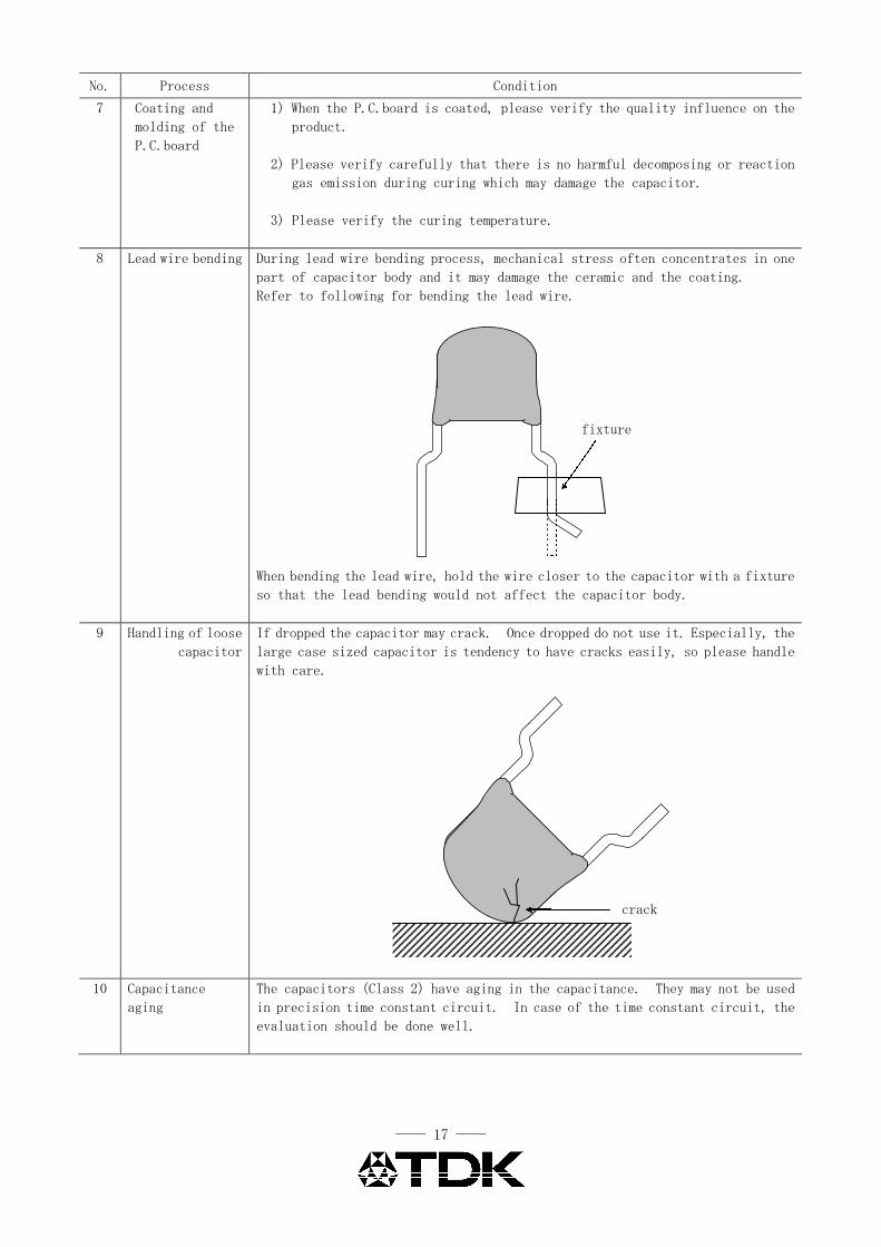
No. Process Condition
7 Coating and
molding of the
P.C.board
1) When the P.C.board is coated, please verify the quality influence on the
product.
2) Please verify carefully that there is no harmful decomposing or reaction
gas emission during curing which may damage the capacitor.
3) Please verify the curing temperature.
8 Lead wire bending During lead wire bending process, mechanical stress often concentrates in one
part of capacitor body and it may damage the ceramic and the coating.
Refer to following for bending the lead wire.
When bending the lead wire, hold the wire closer to the capacitor with a fixture
so that the lead bending would not affect the capacitor body.
9 Handling of loose
capacitor
If dropped the capacitor may crack. Once dropped do not use it. Especially, the
large case sized capacitor is tendency to have cracks easily, so please handle
with care.
10 Capacitance
aging
The capacitors (Class 2) have aging in the capacitance. They may not be used
in precision time constant circuit. In case of the time constant circuit, the
evaluation should be done well.
fixture
crack

―― 18 ――
No. Process Condition
11 Estimated life
and estimated
failure rate
of capacitors
The estimated life and the estimated failure rate depend on the temperature and the
voltage. This can be calculated by the equation described in JEITA RCR-2335B Annex
F(Informative) Calculation of the estimated lifetime and the estimated failure rate
(Temperature acceleration : 3rd powered low, Voltage acceleration : 10degC law)
The failure rate can be decreased by reducing the temperature and the voltage but
they will not be guaranteed.
12 Others
Caution
The products listed on this specification sheet are intended for use in general
electronic equipment (AV equipment, telecommunications equipment, home appliances,
amusement equipment, computer equipment, personal equipment, office equipment,
measurement equipment, industrial robots) under a normal operation and use
condition.
The products are not designed or warranted to meet the requirements of the
applications listed below, whose performance and/or quality require a more stringent
level of safety or reliability, or whose failure, malfunction or trouble could cause
serious damage to society, person or property. Please understand that we are not
responsible for any damage or liability caused by use of the products in any of
the applications below or for any other use exceeding the range or conditions set
forth in this specification sheet.
Aerospace/Aviation equipment. Transportation equipment (cars, electric trains,
ships, etc.) Medical equipment. Power-generation control equipment. Atomic
energy-related equipment. Seabed equipment. Transportation control equipment.
Public information-processing equipment. Military equipment. Electric heating
apparatus, burning equipment. Disaster prevention/crime prevention equipment.
Safety equipment. Other applications that are not considered general-purpose
applications.
When using this product in general-purpose applications, you are kindly requested
to take into consideration securing protection circuit/equipment or providing backup
circuits, etc., to ensure
higher safety.

―― 19 ――
TAPE PACKAGING SPECIFICATION

―― 20 ――
1. CONSTRUCTION AND DIMENSION OF TAPING
Dimensions of FK1* type shall be according to Appendix 2.
Dimensions of FK2* type shall be according to Appendix 3.
2. QUANTITY
Type Parts quantity/box (pcs.)
FK18, FK28
FK14, FK24
FK16, FK26
2,000
FK11, FK20
FK221,500
3. PERFORMANCE SPECIFICATIONS
3-1. The missing of components shall be within consecutive 3pcs.
3-2. Empty part for min 3pcs shall be provided at the beginning and the end of taping.
3-3. Shipping label must be attached at the side of carton.
3-4. When pull the carrier tape for left side with keeping the head of capacitors to
the direction of the above figure, adhesive tape shall be upper side.
3-5. Folded tape shall contain 25pcs. of components.

―― 21 ――
Appendix 2 Taping dimensions
(FK18,FK14,FK16,FK11)
(Unit:mm)
Symbol Dimensions Tolerance
P 12.7 ±1.0
P0 ※1 12.7 ±0.3
P1 5.1 ±0.7
P2 6.35 ±1.3
W0 12.0 ±1.0
W1 9.0 ±0.5
W2 ※2 3.0 3.0 and under
W3 18.0 +1.0,-0.5
H0 16.0 ±0.5
1.0 1.0 and under
t 0.6 ±0.2
L0 11.0 11.0 and under
F 2.5 +0.5,-0.2
φd φ0.5 +0.1,-0.03
φD φ4.0 ±0.2
Δh ――― ±2
※1 Accumulated pitch tolerance shall be ±2mm for 20 pitches.
※2 Adhesive tape shall not stick out from carrier tape.
P2 P P
P1 F
P0 φd φD
H0
W2
W1
W3
t
Δh
W0
L0

―― 22 ――
Appendix 3 Taping dimensions
(FK28,FK24,FK26,FK20,FK22)
(Unit:mm)
Symbol Dimensions Tolerance
P 12.7 ±1.0
P0 ※1 12.7 ±0.3
P1 3.85 ±0.7
P2 6.35 ±1.3
W0 12.0 ±1.0
W1 9.0 ±0.5
W2 ※2 3.0 3.0 and under
W3 18.0 +1.0,-0.5
H0 16.0 ±0.5
1.0 1.0 and under
t 0.6 ±0.2
L0 11.0 11.0 and under
F 5.0 +0.8,-0.2
φd φ0.5 +0.1,-0.03
φD φ4.0 ±0.2
Δh ――― ±2
※1 Accumulated pitch tolerance shall be ±2mm for 20 pitches.
※2 Adhesive tape shall not stick out from carrier tape.
t
P2 P P
P1 F
P0 φd φD
W2
W1
W3
Δh
H0
W0
L0


![Ppt2 c9 [recuperado]](https://img.pdfslide.us/doc/110x75/555b9538d8b42acd238b5438/ppt2-c9-recuperado.jpg)