Embed Size (px)
Citation preview

SpecificationPart Number: Version: Date:
Revision
Midas Components Limited Electra House 32 Southtown Road Great Yarmouth Norfolk NR31 0DU England
Telephone +44 (0)1493 602602 Fax +44 (0)1493 665111 Email [email protected] Website www.midasdisplays.com
VERSION DATE REVISED PAGE NO. Note
0 2016/03/23 First issue A
2016/07/25 Modify Interface Modify Absolute
Maximum Ratings

Contents 1.Module Classification Information
2.Summary
3.General Specification
4.Interface
5.Contour Drawing
6.Block Diagram
7.Absolute Maximum Ratings
8.Electrical Characteristics
9.DC Characteristics
10.AC Characteristics
11.Optical Characteristics
12.Reliability
13.Other
2.Summary This technical specification applies to 7.0’ color TFT-LCD panel. The 7.0’ color TFT-LCD panel is designed for camcorder, digital camera application and other electronic products which require high quality flat panel displays. This module follows RoHS.

3.General Specifications Size: 7.0 inch
Dot Matrix: 800 x RGBx480(TFT) dots
Module dimension: 165.0(W) x 100(H) x 5.8(D) mm
Active area: 154.08 x 85.92 mm
Dot pitch: 0.0642 x 0.179 mm
LCD type: TFT, Normally White, Transmissive
View Direction: 12 o’clock
Gray Scale Inversion Direction: 6 o’clock
Backlight Type: LED, Normally White
With /Without TP: Without TP
Surface: Anti-Glare
*Color tone slight changed by temperature and driving voltage.

Midas Active Matrix Display Part Number System
MC T 057 A 6 * W 320240 L M L * *1 2 3 4 5 6 7 8 9 10 11 12 13
1 = MC: Midas Components
2 = T: TFT A: Active Matrix OLED M: Monitor
3 = Size
4 = Series
5 = Viewing Angle: 6: 6 O’clock 12: 12 O’clock O: All Round Viewing Angle
6 = Blank: No Touch T: Resistive Touchscreen C: Capacitive Touchscreen
7 = Operating Temp Range: S: 0+50Deg C B: -20+60Deg C W: -20+70Deg C E: -30+85Deg C X: -30+80Deg C 8 = No of Pixels
9 = Orientation: P: Portrait L: Landscape 10 = Mode: R: Reflective M: Transmissive T: Transflective S: Sunlight Readable (Transmissive) W: White on Black (Monochrome) 11 = Backlight: Blank: None L: LED C: CCFL 12 = Blank: No Module/board C: Controller board module (E-Tech)
13 = Blank: None OB: Optically Bonded IPS: In‐plane switching

4.Interface 4.1. LCM PIN Definition Pin Symbol Function Remark 1 VLED- Backlight ground 2 VLED+ Power supply for backlight 3 GND Power ground 4 VCC Power for Digital Circuit 5 R0 Red data(LSB) Note 1 6 R1 Red data Note 1 7 R2 Red data 8 R3 Red data 9 R4 Red data 10 R5 Red data 11 R6 Red data 12 R7 Red data(MSB) 13 G0 Green data(LSB) Note 1 14 G1 Green data Note 1 15 G2 Green data 16 G3 Green data 17 G4 Green data 18 G5 Green data 19 G6 Green data 20 G7 Green data(MSB) 21 B0 Blue data(LSB) Note 1 22 B1 Blue data Note 1 23 B2 Blue data 24 B3 Blue data 25 B4 Blue data 26 B5 Blue data 27 B6 Blue data 28 B7 Blue data(MSB) 29 GND Power Ground 30 CLK Sample clock Note 2 31 R/L Right /Left selection Note 3,4 32 Hsync Horizontal Sync Input 33 Vsync Vertical Sync Input 34 NC No connection 35 U/D Up/down selection Note 3,4 36 RESET Global reset pin. 37 NC No connection 38 NC No connection 39 NC No connection 40 NC No connection

Note 1: When input 18 bits RGB data, the two low bits of R,G and B data must be grounded. Note 2: Data shall be latched at the falling edge of CLK. Note 3: Selection of scanning mode Setting of scan control
Scanning direction U/D R/L L H Up to down, left to rightH L Down to up, right to leftL L Up to down, right to leftH H Down to up, left to right
Note 4: Definition of scanning direction. Refer to the figure as below:
Up
Down
Left Right

5.Contour Drawing
The non-specified tolerance of dimension is 0.3mm.
A1
7
15
1716
11
1314
12
910
8
3
56
4
12
GNDVLED+
R0
R2R1
VCC
R4
R6R5
G3
G1G0R7
G4G5
G2
R3
18G619G720
VLED-
35
3940
3738
36
31
3334
32
2930
R/LCLK
U/DNC
NCRESET
GND
2221 B0
B1B223B324B425
B627B728
B526
HsyncVsync
NCNCNC
57.2*32.3mm? ¦ â³ z
© ú̈ ¾² k? ? T=0.05mm
¤¥̧ ó? °ì10.0*8.0mm? ¦ â³ z
© ú̈ ¾² k? ? T=0.05mm
© ö§é? ?
14XL YD XR YU
RTP PAD W=0.6mmP1.0*3=3.0mm
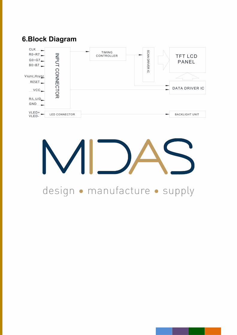
6.Block Diagram
INP
UT
CO
NN
EC
TO
R
G0~G7
R0~R7
CLK
B0~B7
GND
TIMINGCONTROLLER
SC
AN
DR
IVE
R IC
TFT LCDPANEL
DATA DRIVER IC
LED CONNECTOR BACKLIGHT UNIT
Vsync,Hsync
R/L,U/D
VLED+
RESET
VCC
VLED-

7.Absolute Maximum Ratings
Item Symbol Min Typ Max Unit
Operating Temperature TOP -20 - +70
Storage Temperature TST -30 - +80
Note: Device is subject to be damaged permanently if stresses beyond those absolute maximum ratings listed above
Temp. 60 , 90% RH MAX. Temp.>60 , Absolute humidity shall be less than 90% RH at 60

8.Electrical Characteristics 8.1. Operating conditions:
Item Symbol Min Typ Max Unit Remark
Supply Voltage For Logic VCC 3.0 3.3 3.6 V Note 1
Power Supply For Current VCC =3.3V 110 165 mA
Note 1 : This value is test for Vcc=3.3V , Ta=25℃ only
8.2. LED driving conditions
Parameter Symbol Min. Typ. Max. Unit Remark LED current - - 180 - mA - Power Consumption - 1620 - 1890 mW - LED voltage VLED+ 9.0 - 10.5 V Note 1
LED Life Time - - 50,000 - Hr Note 2,3,4
Note 1 : There are 1 Groups LED
Note 2 : Ta = 25 ℃ Note 3 : Brightness to be decreased to 50% of the initial value Note 4 : The single LED lamp case

9.DC CHARATERISTICS
Parameter Symbol Rating
Unit Condition Min Typ Max
Low level input voltage VIL 0 - 0.3VCC V
High level input voltage VIH 0.7VCC - VCC V

10.AC CHARATERISTICS 10.1. AC Electrical Characteristics
Signal Symbol Min Typ Max Unit HS setup time Thst 8 - - ns HS hold time Thhd 8 - - ns VS setup time Tvst 8 - - ns VS hold time Tvhd 8 - - ns Data setup time Tdsu 8 - - ns Data hole time Tdhd 8 - - ns VCC Power On Slew rate TPOR - - 20 ms RESET pulse width TRst 1 - - ms DCLK cycle time Tcoh 20 - - ns DCLK pulse duty Tcwh 40 50 60 %
10.2. Input Clock and Data Timing Diagram

10.3. Timing
Item SymbolValues
Unit RemarkMin. Typ. Max.
CLK Frequency (DCLK) fclk 26.4 33.3 46.8 MHz Horizontal Display Area thd - 800 - CLK
One Horizontal Line th 862 1056 1200 CLK HS pulse width thpw 1 - 40 CLK HS Blanking thb 46 46 46 CLK HS Front Porch thfp 16 210 354 CLK Vertical Display Area tvd - 480 - TH VS period time tv 510 525 650 TH VS pulse width tvpw 1 - 20 TH
VS Blanking tvb 23 23 23 TH
VS Front Porch tvfp 7 22 147 TH 10.4. Data Input Format
Fig. Horizontal input timing diagram
Fig. Vertical input timing diagram

11.Optical Characteristics Item Symbol Condition. Min Typ. Max. Unit Remark
Response time Tr
θ=0°、Φ=0° - 10 20 .ms
Note 3 Tf - 15 30 .ms
Contrast ratio CR At optimized viewing angle
400 500 - - Note 4
Color Chromaticity White Wx
θ=0°、Φ=0 0.26 0.31 0.36 -
Note 2,5,6Wy 0.28 0.33 0.38 -
Viewing angle (Gray Scale Inversion
Direction)
Hor. ΘR
CR≧10
60 70 -
Deg. Note 1 ΘL 60 70 -
Ver. ΦT 40 50 - ΦB 60 70 -
Brightness - - 350 460 - cd/m 2 Center of display
Ta=25±2 , IL=180mA Note 1: Definition of viewing angle range
Fig. 11.1. Definition of viewing angle Note 2: Test equipment setup: After stabilizing and leaving the panel alone at a driven temperature for 10 minutes, the measurement should be executed. Measurement should be executed in a stable, windless, and dark room. Optical specifications are measured by Topcon BM-7orBM-5 luminance meter 1.0° field of view at a distance of 50cm and normal direction.
Fig. 11.2. Optical measurement system setup

Note 3: Definition of Response time: The response time is defined as the LCD optical switching time interval between “White” state and “Black” state. Rise time, Tr, is the time between photo detector output intensity changed from 90%to 10%. And fall time, Tf, is the time between photo detector output intensity changed from 10%to 90%
B la c k ( T F T O N ) W h i te ( T F T O F F )W h i te ( T F T O F F )1 0 0 %9 0 %
1 0 %0 %
D is p l a yD a t a
Note 4: Definition of contrast ratio: The contrast ratio is defined as the following expression.
Lum inance m easured w hen LC D on the "W hite" stateC ontrast ratio (C R ) =
Lum inance m easured w hen LC D on the "B lack" state Note 5: White Vi = Vi50 ± 1.5V Black Vi = Vi50 ± 2.0V “±” means that the analog input signal swings in phase with VCOM signal. “±” means that the analog input signal swings out of phase with VCOM signal. The 100% transmission is defined as the transmission of LCD panel when all the input terminals of module are electrically opened. Note 6: Definition of color chromaticity (CIE 1931) Color coordinates measured at the center point of LCD Note 7: Measured at the center area of the panel when all the input terminals of LCD panel are electrically opened.

12.Reliability Content of Reliability Test (Wide temperature, -20 ~70 )
Note1: No dew condensation to be observed. Note2: The function test shall be conducted after 4 hours storage at the normal Temperature and humidity after remove from the test chamber. Note3: The packing have to including into the vibration testing.
Environmental Test
Test Item Content of Test Test Condition Note High Temperature storage
Endurance test applying the high storage temperature for a long time.
80 200hrs
2
Low Temperature storage
Endurance test applying the low storage temperature for a long time.
-30 200hrs
1,2
High Temperature Operation
Endurance test applying the electric stress (Voltage & Current) and the thermal stress to the element for a long time.
70 200hrs
——
Low Temperature Operation
Endurance test applying the electric stress under low temperature for a long time.
-20 200hrs
1
High Temperature/ Humidity Operation
The module should be allowed to stand at 60 ,90%RH max
60 ,90%RH 96hrs
1,2
Thermal shock resistance
The sample should be allowed stand the following 10 cycles of operation -20 25 70 30min 5min 30min 1 cycle
-20 /70 10 cycles
——
Vibration test Endurance test applying the vibration during transportation and using.
Total fixed amplitude : 15mm Vibration Frequency : 10~55Hz One cycle 60 seconds to 3 directions of X,Y,Z for Each 15 minutes
3
Static electricity test Endurance test applying the electric stress to the terminal.
VS=±600V(contact),±800v(air), RS=330Ω CS=150pF 10 times
——