Embed Size (px)
Citation preview

Specification for TFT
AFR240320A0-1.77INTM-I
Revision V1.0
A Orient Display
FR TFT Type
240320 Resolution 240 x 320
A0 Serial A0
1.77 1.77'', Module Dimension 34.70 x 46.70 x 2.5 mm
I IPS Display
N Top: -20~+70°C; Tstr: -30~+80°C
T Transmissive/Normally Black
M Medium Brightness, 500cd/m2
/ No Touch Panel
/ Controller JD9852
/ MIPI + one data lane Interface

Revision History
Date Rev. No. Page Summary
2019.07.15 V1.0 ALL FIRST ISSUE
Orient Display (N.A.) Ltd.
220 Royal Crest Court,Unit 06,Markham,ON,Canada L3R 9Y2 Tel: 905-477-1166 Fax: 905-477-1782
Orient Display (USA) Corp. 14925 SE Allen Road, Suite 203 B, Bellevue, WA 98006 Tel: (425)698-1938 Fax: (425)698-1852

AFR240320A0-1.77INTM-I Page 3
Contents 1. Basic Information ............................................................................ 4
1.1 Features ........................................................................................................ 4 1.2 Mechanical Information ................................................................................. 4
2. Block Diagram ................................................................................. 5
3. Outline Dimension ........................................................................... 6
4. Input terminal Pin Assignment ....................................................... 7
5. LCD Optical Characteristics ........................................................... 8
5.1 Optical specification ...................................................................................... 8
5.2 Measuring Condition ..................................................................................... 8 5.3 Measuring Equipment ................................................................................... 9
6. Electrical Characteristics.............................................................. 11
6.1 Absolute Operation Rating (Ta=25 VSS=0V) .............................................. 11
6.2 DC Electrical Characteristics ...................................................................... 11 6.3 LED Backlight Characteristics ..................................................................... 12
7. AC Characteristic .......................................................................... 14
7.1 Reset Input Timing ...................................................................................... 14
7.2 Timings for DSI Video mode ....................................................................... 15
8. LCD Module Out-Going Quality Level .......................................... 17
8.1 VISUAL & FUNCTION INSPECTION STANDARD ..................................... 17 8.1.1 Inspection conditions ............................................................................................. 17 8.1.2 Definition ............................................................................................................... 17 8.1.3 Sampling Plan ....................................................................................................... 18 8.1.4 Criteria (Visual) ...................................................................................................... 19
9. Reliability Test Result ................................................................... 22
10. Cautions and Handling Precautions ...................................... 23
10.1 Handling and Operating the Module ........................................................... 23
10.2 Storage and Transportation. ....................................................................... 23
11. Packing .................................................................................... 24

AFR240320A0-1.77INTM-I Page 4
1. Basic Information
* Description
This is a color active matrix TFT (Thin Film Transistor) LCD (liquid crystal display) that uses amorphous silicon TFT as a switching device. This module is composed of a Transmissive type TFT-LCD Panel, driver circuit, back-light unit. The resolution of a 1.77’’TFT-LCD contains 240X320 pixels, and can display up to 65K/262K colors.
1.1 Features
General Information Items
Specification Unit Note
Main Panel
Display area(AA) 26.64(H)*35.52(V) (1.77inch) mm -
Driver element TFT active matrix - -
Display colors 65K/262K colors -
Number of pixels 240(RGB)*320 dots -
Pixel arrangement RGB vertical stripe - -
Pixel pitch 0.111(H)*0.111(V) mm -
Viewing angle ALL o'clock -
Controller IC JD9852 - -
LCM Interface MIPI+one data lane - -
Display mode Transmissive/Normally Black - -
Operating temperature -20~+70 ℃ -
Storage temperature -30~+80 ℃ -
1.2 Mechanical Information
Item Min. Typ. Max. Unit Note
Module size
Horizontal(H) 34.7 mm -
Vertical(V) 46.7 mm -
Depth(D) 2.5 mm -
Weight 6 g -

AFR240320A0-1.77INTM-I Page 5
2. Block Diagram

AFR240320A0-1.77INTM-I Page 6
3. Outline Dimension
20 19 18 17
RE
SE
T
IOV
CC
NC
LED
A
16 15 14 13 12 11 10 9 8 7 6 5 4 3 2 1
NO
.
NC
LED
K
VC
I
GN
D
GN
D
MIP
I_D0N
MIP
I_D0P
MIP
I_CLN
MIP
I_CLP
GN
D
NC NC
GN
D
TE
GN
D
NC
AK
V0
TF
T
THIS D
RAW
ING
IS PROPERTY O
F ORIEN
T DISPLA
Y.
ALL RIG
HTS RESERVED
.
FIT
mm
1 of 1Y
ES
±0.3
FIR
ST ISSU
EJU
N-01-2019
V0
IPS/NO
RM
AL
BL
AC
K1.77" 240*320 PIX
EL
ST
RA
NSM
ISSIVE
FR
EE
-20°C T
O +
70°C-30°C
TO
+80°C
1.8V ~
3.3V3.3V/
JD9852
3 LE
D,W
HIT
E, 20m
A, 9.6±
0.3V
ZIF
AF
R240320A
0-1.77INT
M-I
AF
R240320A
0-1.77INT
M-I
167
RGR
240RGB*320All O
'Clock
201
1.35
2.50±0.2(Module)
0.30±0.03(Conduct+Stiffener)
0.13±0.03
ConductStiffener
DOUBLE SIDE TAPE
(T=0.10mm)
DOUBLE SIDE TAPE
(T=0.10mm)
0.80MAX
componentarea
10.50±0.1P
0.5*19=9.50±0.05W
=0.30
0.50
3.50
26.64 LCD
AA
35.52 LCD AA
34.70±0.2 BL
46.70±0.2 BL
3.204.03
29.35±0.5
1.82±0.3
1.45±0.3
12.10±0.3
29.64 UP
PO
L30.54
38.32 UP POL
42.92
2.531.70
FRONT
BACK
34.70
3.00
23.00
3.00
12.10±0.3
28.20±0.50.80MAX
10.00
FPC bending reference figure
FPC unfold shipment
201
component
area
8.50
9.20
3.00(Mark line)
5.00(Pi)
R1
1.20MA
XCom
ponent
Pull Tape
17.20
Yellow
tape
AFR240320A0-1.77INTM-I Page 7
4. Input terminal Pin Assignment
Pin NO.
Symbol Function I/O
1 NC
2 LEDK Cathode pin of backlight. P
3 NC
4 LEDA Anode pin of backlight. P
5 NC
6 VCI Supply voltage (3.3V). P
7 IOVCC Power supply for I/O block(1.8-3.3V) P
8 TE Serve as a TE (Tearing Effect) output signal O
9 RESET Reset pin. Setting either pin low initializes the LSI. Must be reset after power is supplied.
I
10 GND Ground. P
11 NC
12 NC
13 GND Ground. P
14 MIPI_CL
P DSI Positive polarity of low voltage differential clock signal
I
15 MIPI_CL
N
DSI Negative polarity of low voltage differential clock signal
16 GND Ground. P
17 MIPI_D0
P DSI Positive polarity of low voltage differential data signal
I
18 MIPI_D0
N DSI Negative polarity of low voltage differential data signal
I
19 GND Ground. P
20 GND Ground. P

AFR240320A0-1.77INTM-I Page 8
5. LCD Optical Characteristics
5.1 Optical specification
Item Symbol Condition Min. Typ. Max. Unit. Note
Contrast Ratio CR Θ=0
Normal
viewing
angle
500 600 *
Response
time
Rising
TR+TF -- 35 50 msec * Falling
Color gamut S(%) -- 49.3 -- % *
Color Filter
Chromacicity
White WX 0.2454 0.2854 0.3254
CA310
Test
WY 0.2716 0.3116 0.3516
Red RX 0.5604 0.6004 0.6404
RY 0.3208 0.3608 0.4008
Green GX
0.2958 0.3358 0.3758
GY 0.5142 0.5542 0.5942
Blue BX 0.1198 0.1598 0.1998
BY 0.0732 0.1132 0.1532
Viewing
angle
Hor. ΘL
CR>10
60 85 --
* ΘR 60 85 --
Ver. ΘU 60 85 --
ΘD 60 85 --
Option View
Direction ALL
*The data comes from the LCD specification.
5.2 Measuring Condition
■ Measuring surrounding:dark room
■ Ambient temperature:25±2℃
■ 15min. warm-up time.

AFR240320A0-1.77INTM-I Page 9
5.3 Measuring Equipment

AFR240320A0-1.77INTM-I Page 10

AFR240320A0-1.77INTM-I Page 11
6. Electrical Characteristics
6.1 Absolute Operation Rating (Ta=25 VSS=0V)
Item Symbol Rating Unit
Supply Voltage VCI -0.3~4.6 V
Digital interface supply Voltage IOVCC -0.3~4.6 V
Operating temperature TOP -20~+70 ℃
Storage temperature TST -30~+80 ℃
Note: If one of the above items is exceeded its maximum limitation momentarily, the quality of the product may be degraded. Absolute maximum limitation, therefore, specify the values exceeding which the product may be physically damaged. Be sure to use the product within the recommend range.
6.2 DC Electrical Characteristics
Parameter Symbol Min. Typ. Max. Unit Note
Supply Voltage VCI 2.4 3.3 3.6 V
Digital interface supply
Voltage IOVCC 1.65 1.8 3.3 V
Normal mode Current
consumption IDD -- TBD -- mA
Level input voltage VIH
0.7
IOVCC IOVCC V
VIL GND 0.3 IOVCC V
Level output voltage VOH
0.8
IOVCC IOVCC V
VOL GND 0.2 IOVCC V

AFR240320A0-1.77INTM-I Page 12
6.3 LED Backlight Characteristics
The back-light system is edge-lighting type with 4 chips White LED
Item Symbol Min. Typ. Max. Unit Note
Forward Current IF 15 20 -- mA
Forward Voltage VF -- 9.6 -- V
LCM Luminance LV 450 500 -- cd/m2 Note3
LED life time Hr 50000 -- -- Hour Note1,2
Uniformity AVg 80 -- -- ﹪ Note3
Note (1) LED life time (Hr) can be defined as the time in which it continues to
operate under the condition: Ta=25±3 ℃, typical IL value indicated in the above
table until the brightness becomes less than 50%.
Note (2) The “LED life time” is defined as the module brightness decrease to 50%
original brightness at Ta=25℃ and IL=20mA. The LED lifetime could be decreased if
operating IL is larger than 20mA. The constant current driving method is suggested.
A K

AFR240320A0-1.77INTM-I Page 13
NOTE 3:Luminance Uniformity of these 9 points is defined as below:
Luminance=9
points 9 of Luminance Total

AFR240320A0-1.77INTM-I Page 14
7. AC Characteristic
7.1 Reset Input Timing
* Reset input timings

AFR240320A0-1.77INTM-I Page 15
7.2 Timings for DSI Video mode

AFR240320A0-1.77INTM-I Page 16

AFR240320A0-1.77INTM-I Page 17
8. LCD Module Out-Going Quality Level
8.1 VISUAL & FUNCTION INSPECTION STANDARD
8.1.1 Inspection conditions
Inspection performed under the following conditions is recommended.
Temperature : 25±5℃
Humidity : 65%±10%RH Viewing Angle : Normal viewing Angle. Illumination: Single fluorescent lamp (300 to 700Lux) Viewing distance:30-50cm
8.1.2 Definition
Zone A : Effective Viewing Area(Character or Digit can be seen) Zone B : Viewing Area except Zone A Zone C : Outside (Zone A+Zone B) which can not be seen after assembly by customer .)
Zone D : IC Bonding Area Note: As a general rule ,visual defects in Zone C can be ignored when it doesn’t effect product
function or appearance after assembly by customer
Upper
Glass
Upper Polarizer
Bottom glass
Bottom Polarizer Light Source
Zone A Zone B
Zone C
Zone D
AFR240320A0-1.77INTM-I Page 18
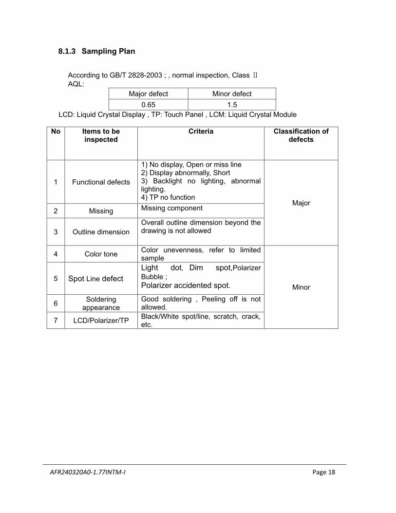
8.1.3 Sampling Plan
According to GB/T 2828-2003 ; , normal inspection, Class Ⅱ
AQL:
Major defect Minor defect
0.65 1.5
LCD: Liquid Crystal Display , TP: Touch Panel , LCM: Liquid Crystal Module
No Items to be inspected
Criteria Classification of defects
1 Functional defects
1) No display, Open or miss line 2) Display abnormally, Short 3) Backlight no lighting, abnormal lighting. 4) TP no function
Major 2 Missing Missing component
3 Outline dimension
Overall outline dimension beyond the drawing is not allowed
4 Color tone Color unevenness, refer to limited sample
Minor
5 Spot Line defect
Light dot,Dim spot,Polarizer
Bubble ;
Polarizer accidented spot.
6 Soldering
appearance
Good soldering , Peeling off is not allowed.
7 LCD/Polarizer/TP Black/White spot/line, scratch, crack, etc.

AFR240320A0-1.77INTM-I Page 19
8.1.4 Criteria (Visual)
Number Items Criteria(mm)
1.0 LCD Crack/Broken NOTE: X: Length Y: Width Z: Height L: Length of ITO, T: Height of LCD
(1) The edge of
LCD broken
X Y Z
≤3.0mm <Inner border line of
the seal ≤T
(2)LCD corner broken
X Y Z
≤3.0mm ≤L ≤T
(3) LCD crack
Crack Not allowed

AFR240320A0-1.77INTM-I Page 20
2.0
Spot defect
Y X
Φ=(X+Y)/2
① light dot(LCD/TP/Polarizer black/white spot , light dot,
pinhole, dent, stain)
Zone Size (mm)
Acceptable Qty
A B C
Φ≤0.10 Ignore
Ignore 0.10<Φ≤0.20 3( distance≧10mm)
0.20<Φ≤0.25 2
Φ>0.3 0
②Dim spot(LCD/TP/Polarizer dim dot, light leakage、
dark spot)
Zone Size (mm)
Acceptable Qty
A B C
Φ≤0.1 Ignore
Ignore 0.10<Φ≤0.20 3( distance≧10mm)
0.20<Φ≤0.25 2
Φ>0.3 0
③ Polarizer accidented spot
Zone Size (mm)
Acceptable Qty
A B C
Φ≤0.2 Ignore
Ignore 0.3<Φ≤0.5 2( distance≧10mm)
Φ>0.5 0
④Pixel bad points(light dot,Dim dot, color dot)
Zone Size (mm)
Acceptable Qty
A B C
Φ≤0.1 Ignore Ignore
0.15<Φ≤0.2 2( distance≧10mm)
Φ>0.2 0
⑤ Polarizer Bubble
Zone Size (mm)
Acceptable Qty
A B C
Φ≤0.2 Ignore
Ignore 0.3<Φ≤0.4 3(distance≧10mm)
0.4<Φ≤0.5 2
Φ>0.5 0

AFR240320A0-1.77INTM-I Page 21
3.0
Line defect (LCD/TP /Polarizer backlight
black/white line, scratch,
stain)
Width(mm) Length(mm) Acceptable Qty
A B C
Φ≤0.03 Ignore Ignore
Ignore 0.03<W≤0.04 L≤3.0 N≤2
0.04<W≤0.05 L≤2.0 N≤1
0.05<W Define as spot defect
4.0
Electronic Components SMT
Not allow missing parts,solderless connection,cold solder
joint,mismatch,The positive and negative polarity opposite
5.0 Display color& Brightness
1. Color:Measuring the color coordinates, The measurement
standard according to the datasheet or samples.
2. Brightness:Measuring the brightness of White screen, The
measurement standard according to the datasheet or Samples.
6.0 LCD Mura By 5% ND filter invisible.
Criteria ( functional items)
Number 1 2 3 4
Items No display
Missing segment Short
Backlight no lighting
Criteria (mm) Not allowed Not allowed Not allowed Not allowed

AFR240320A0-1.77INTM-I Page 22
9. Reliability Test Result
Remark:
1.The test samples should be applied to only one test item.
2.Sample size for each test item is 5~10pcs.
3.For Damp Proof Test, Pure water(Resistance>10MΩ) should be used.
4.In case of malfunction defect caused by ESD damage, if it would be recovered to normal state
after resetting, it would be judged as a good part.
5.Failure Judgment Criterion: Basic Specification, Electrical Characteristic, Mechanical
Characteristic, Optical Characteristic.
Item Condition Inspection after
test
High Temperature
Operating 70℃,96H
Inspection after 2~4hours
storage at room
temperature, the sample
shall be free from defects:
1.Air bubble in the LCD;
2.Non-display;
3.Missing segments/line;
4.Glass crack;
5.Current IDD is twice
higher than initial value.
Low Temperature
Operating -20℃, 96HR
High Temperature
Storage 80℃, 96HR
Low Temperature
Storage -30℃, 96HR
High Temperature &
High Humidity Storage +60℃, 90% RH ,96 hours.
Thermal Shock (Non-
operation)
-30℃,30 min ↔ 80℃,30 min,
Change time:5min 20CYC.
ESD test
C=150pF, R=330,5points/panel
Air:±8KV, 5times; Contact:±6KV, 5 times;
(Environment: 15℃~35℃, 30%~60%).
Vibration (Non-
operation)
Frequency range:10~55Hz, Stroke:1.5mm
Sweep:10Hz~55Hz~10Hz 2 hours for each
direction of X.Y.Z. (6 hours for total)
(Package condition).
Box Drop Test 1 Corner 3 Edges 6 faces,80㎝(MEDIUM
BOX)

AFR240320A0-1.77INTM-I Page 23
10. Cautions and Handling Precautions
10.1 Handling and Operating the Module
(1) When the module is assembled, it should be attached to the system firmly. Do not warp or twist the module during assembly work. (2) Protect the module from physical shock or any force. In addition to damage, this may cause improper operation or damage to the module and back-light unit. (3) Note that polarizer is very fragile and could be easily damaged. Do not press or scratch the surface. (4) Do not allow drops of water or chemicals to remain on the display surface. If you have the droplets for a long time, staining and discoloration may occur. (5) If the surface of the polarizer is dirty, clean it using some absorbent cotton or soft cloth. (6) The desirable cleaners are water, IPA (Isopropyl Alcohol) or Hexane. Do not use ketene type materials (ex. Acetone), Ethyl alcohol, Toluene, Ethyl acid or Methyl chloride. It might permanent damage to the polarizer due to chemical reaction. (7) If the liquid crystal material leaks from the panel, it should be kept away from the eyes or mouth. In case of contact with hands, legs, or clothes, it must be washed away thoroughly with soap. (8) Protect the module from static; it may cause damage to the CMOS ICs. (9) Use finger-stalls with soft gloves in order to keep display clean during the incoming inspection and assembly process. (10) Do not disassemble the module. (11) Protection film for polarizer on the module shall be slowly peeled off just before use so that the electrostatic charge can be minimized. (12) Pins of I/F connector shall not be touched directly with bare hands. (13) Do not connect, disconnect the module in the “Power ON” condition. (14) Power supply should always be turned on/off by the item 6.1 Power On Sequence &6.2 Power Off Sequence
10.2 Storage and Transportation.
(1) Do not leave the panel in high temperature, and high humidity for a long time.
It is highly recommended to store the module with temperature from 0 to 35 ℃ and relative humidity
of less than 70% (2) Do not store the TFT-LCD module in direct sunlight. (3) The module shall be stored in a dark place. When storing the modules for a long time, be sure to adopt effective measures for protecting the modules from strong ultraviolet radiation, sunlight, or fluorescent light. (4) It is recommended that the modules should be stored under a condition where no condensation is allowed. Formation of dewdrops may cause an abnormal operation or a failure of the module. In particular, the greatest possible care should be taken to prevent any module from being operated where condensation has occurred inside. (5) This panel has its circuitry FPC on the bottom side and should be handled carefully in order not to be stressed.

AFR240320A0-1.77INTM-I Page 24
11. Packing
2
345
5
6
7
8
1Put module to tray
(Cover Lens down)
After the product is loaded into the TRAY
(as shown in Figure 2), a layer of EPE isadded.
The product is normally loaded in the diagram (3) TRAY
(as shown in Fig. 3, TRAY needs to be rotated 180 degrees), and then it is topped with a layer of EPE,
and stacked with Fig. (2) TRAY.
As shown in figure (5): stackthe OK TRAY, and then seal inthe anti-static bag andvacuum it.
As shown in figure (7), first insert
(6) the package into the outer box
of figure (7), then put the product
of figure (6) into the outer box andseal it with tape.
Carton size : 525x420x220mm.The outer box is sealed into "work"type and relabeled
Paper
Label
As shown in figure (4): After stacking 10 layers of TRAY in figure (2)
and TRAY in figure (3), an empty TRAY is added on top. (Tray size: 360*260*15,
one pack of 3PCS, total 30PCS products)
As shown in figure (6): Anti-staticfoam must be placed in the box, up,down, right, left, and right.
E
MA
XSM080-002A
回收
A
BBB
BBBB
BBBB
B
B BC
C
C
C
D
D
D
DC
PA3000046
V0
THIS D
RAW
ING
IS PROPERTY O
F ORIEN
TD
ISPLAY
. ALL RIG
HTS RESERVED
.
FIT
mm
1 of 1Y
ES
±0.3
FIR
ST ISSU
EM
AR
-12-2020V
0
PackagePackage
Package