Embed Size (px)
Citation preview

Issue 1-0 1 (26)
OPEN BASE STATION ARCHITECTURE INITIATIVE Appendix F Specification for ‘Slim-I/O’ Panel Mount Cable to Board I/O Connector Version 1.0

Issue 1-0 2 (26)
FOREWORD 1
OBSAI description and specification documents are developed 2 within the Technical Working Group of the Open Base Station 3 Architecture Initiative Special Interest Group (OBSAI SIG). 4 Members of the OBSAI TWG serve voluntarily and without 5 compensation. The description and specifications developed 6 within OBSAI represent a consensus of the broad expertise on the 7 subject within the OBSAI SIG. 8
The OBSAI SIG uses the following terminology in the 9 specifications: 10
• "shall" expresses a provision that is binding 11 • "should" and "may" expresses non-mandatory provisions 12 • "will" expresses a declaration of purpose on the part of the 13
OBSAI SIG. It may be necessary to use "will" in cases 14 where the simple future tense is required 15
Use of an OBSAI reference or specification document is wholly 16 voluntary. The existence of an OBSAI Specification does not 17 imply that there are no other ways to produce, test, measure, 18 purchase, market, or provide other goods and services related to 19 the scope of the OBSAI Specification. Furthermore, the viewpoint 20 expressed at the time a specification is approved and issued is 21 subject to change brought about through developments in the 22 state of the art and comments received from users of the 23 specification. Every OBSAI Specification is subjected to review in 24 accordance with the Open Base Station Architecture Initiative 25 Rules and Procedures. 26
Implementation of all or part of an OBSAI Specification may 27 require licenses under third party intellectual property rights, 28 including without limitation, patent rights (such a third party may or 29 may not be an OBSAI Member). The Promoters of the OBSAI 30 Specification are not responsible and shall not be held responsible 31 in any manner for identifying or failing to identify any or all such 32 third party intellectual property rights. 33
The information in this document is subject to change without 34 notice and describes only the product defined in the introduction of 35 this documentation. This document is intended for the use of 36 OBSAI Member’s customers only for the purposes of the 37 agreement under which the document is submitted, and no part of 38 it may be reproduced or transmitted in any form or means without 39 the prior written permission of OBSAI Management Board. The 40 document has been prepared for use by professional and properly 41

Issue 1-0 3 (26)
trained personnel, and the customer assumes full responsibility 1 when using it. 2
OBSAI Management Board, Marketing Working Group and 3 Technical Working Group welcome customer comments as part of 4 the process of continuous development and improvement of the 5 documentation. 6
The information or statements given in this document concerning 7 the suitability, capacity, or performance of the mentioned hardware 8 or software products cannot be considered binding but shall be 9 defined in the agreement made between OBSAI members. 10 However, the OBSAI Management Board, Marketing Working 11 Group or Technical Working Group have made all reasonable 12 efforts to ensure that the instructions contained in the document 13 are adequate and free of material errors and omissions. 14
OBSAI liability for any errors in the document is limited to the 15 documentary correction of errors. OBSAI WILL NOT BE 16 RESPONSIBLE IN ANY EVENT FOR ERRORS IN THIS 17 DOCUMENT OR FOR ANY DAMAGES, INCIDENTAL OR 18 CONSEQUENTIAL (INCLUDING MONETARY LOSSES), that 19 might arise from the use of this document or the information in it. 20
This document and the product it describes are considered 21 protected by copyright according to the applicable laws. OBSAI 22 logo is a registered trademark of Open Base Station Architecture 23 Initiative Special Interest Group. Other product names mentioned 24 in this document may be trademarks of their respective 25 companies, and they are mentioned for identification purposes 26 only. Copyright © Open Base Station Architecture Initiative 27 Special Interest Group. All rights reserved. Users are cautioned 28 to check to determine that they have the latest edition of any 29 OBSAI Specification. 30
Interpretations: Occasionally questions may arise regarding the 31 meaning of portions of standards as they relate to specific 32 applications. When the need for interpretations is brought to the 33 attention of OBSAI, the OBSAI TWG will initiate action to prepare 34 appropriate responses. Since OBSAI Specifications represent a 35 consensus of OBSAI Member’s interests, it is important to ensure 36 that any interpretation has also received the concurrence of a 37 balance of interests. For this reason OBSAI and the members of 38 its Technical Working Groups are not able to provide an instant 39 response to interpretation requests except in those cases where 40 the matter has previously received formal consideration. 41

Issue 1-0 4 (26)
Comments on specifications and requests for interpretations 1 should be addressed to: 2
Peter Kenington 3
Chairman, OBSAI Technical Working Group 4
Andrew 5

Issue 1-0 5 (26)
Contents 1 2
1 Summary of changes.....................................................................................6 3 2 Scope ..............................................................................................................7 4 3 General Description .......................................................................................8 5 4 Ratings............................................................................................................9 6 5 Electrical Specification (Ratings) ...............................................................10 7 6 Mechanical Specification.............................................................................11 8 7 Environmental Requirement .......................................................................15 9
7.1 Environment specification for transportation ...........................................15 10 8 PCB Layout and Minimum Connector Spacing .........................................15 11 9 Panel Cut-Out ...............................................................................................17 12 10 Panel Mounting Inserts ............................................................................18 13 11 Specification Drawings ............................................................................19 14 12 Mating Dimensions...................................................................................20 15 13 Cable Assembly Specification.................................................................23 16 12.1 Electrical Specifications: .........................................................................23 17
12.1.1 Insertion Loss Lower Limit for L=3m Long, High Speed Cable 18 Assembly:.........................................................................................23 19
12.1.2 Insertion Loss Lower Limit for L=3m Long, Low Speed Cable 20 Assembly:.........................................................................................23 21
12.1.3 Return Loss Lower Limit for L=3m Long, High Speed Cable 22 Assembly:.........................................................................................24 23
12.1.4 Return Loss Lower Limit for L=3m Long, Low Speed Cable 24 Assembly:.........................................................................................24 25
12.2 Cable Assembly Impedance Profile (TDR method):................................24 26 12.3 Cable Assembly (L=3m Long) Total Differential Noise (TDR method): ...25 27 12.4 Differential Skew (L=3m Long):...............................................................25 28 14 Reference Documents..............................................................................26 29 30

Issue 1-0 6 (26)
1 Summary of changes 1
2
Version Approved by Date
1.0 Management Board June 28, 2006
3

Issue 1-0 7 (26)
2 Scope 1
2
Specification for: 3
Panel Mount I/O cable Connector for RF Module in Base Transmission System. 4

Issue 1-0 8 (26)
3 General Description 1
2
• Type: I/O 3
• Connection method: Panel Mount – Cable to Board 4
• Shape: Rectangle 5
• Number of positions: 16 6
7
8
9
10
11
Figure 1: ‘Slim-I/O’, Right Angle Receptacle & Cable Plug. 12
Issue 1-0 9 (26)
4 Ratings 1
2
• Max. Voltage (U): 50 VDC 3
• Max. Current (I): 1.0 A at 30°C temp. rise above ambient 4
• Operational temperature range: -10…+60 °C 5
• Relative Humidity: 10% to 90% 6
• Characteristic Impedance: 100Ω ± 10% (Differential) 7
• Data Rate: Up to 3.125Gbps 8

Issue 1-0 10 (26)
5 Electrical Specification (Ratings) 1
Parameter Requirement Procedure
Dry circuit resistance
70 mΩ maximum. ΔR 20 mΩ maximum.
EIA-364-23. Subject specimens to 100mA maximum and 20mV maximum open circuit voltage. See Figure 2.
2 Insulation resistance
1000 MΩ minimum EIA-364-21. Test between adjacent contacts of unmated specimens.
3 Dielectric withstanding voltage
350 VAC at sea level. 1 minute hold with no breakdown or flashover.
EIA-364-20 Condition I. Test between adjacent contacts of unmated specimens.
4 Impedance, Single Ended / Differential
ZSE(Ω) ± 10% ZDIFF(Ω) ± 10%
Measured with TDR @ Rise time =100ps (10% -to- 90%)
5 Eye pattern. Differential – Normalized
0.8 minimum @ 50% of UI Stimulated 1VPtP Differential PRBS 211-1. Measured Procedure EIA 364-107
6 Insertion loss, Diff. Mixed Mode (SDD21)
1.0 dB max. @ f ≤ 2.5 GHz ≤ - 2.0 dB @ (f) up to 5 GHz
Measured Procedure EIA 364-101
7 Return loss, Diff. Mixed Mode (SDD11)
≤ -10 dB @ f ≤ 2.5 GHz ≤ -5 dB @ (f) up 5 GHz
Measured Procedure EIA 364-108
8 Near end Noise, Differential (Isolation)
-28dB max. up to 2.5GHz ≤ -26 dB @ (f) up 5 GHz
Measured Procedure EIA 364-90

Issue 1-0 11 (26)
6 Mechanical Specification 1
• All mechanical dimensions are described in drawings in chapter 8. 2
• Allowed misalignment (Plug relative to Receptacle): 3 Longitudinal ≤ ± 25° 4 Vertical ≤ ± 6° 5
• Basic material of the body: 6 Housing – Thermoplastic, UL94V-0, Black 7 Shell: Copper Alloy 8 Jack Screw Spacer – Thermoplastic, UL94V-0, Black 9
• Contact material: 10 Receptacle – Phosphor Bronze 11 Plug – PCB Substrate. FR4 with Au Plated Copper 12
Conductors 13
• PCB Termination: Plated Through Hole – Solder Type as well 14 as Pin In Paste compatible 15
• Weight (g): 9.0 gr. ± 0.5 gr. 16
• Connector must be compatible with RoHS requirements. 17
Parameter Requirement Procedure
Solderability
Solderable area shall have a minimum of 95% solder coverage.
EIA-364-638. Subject contacts to Solderability.
18 Vibration, random
No discontinuities of 1 μsec. Or longer duration. See Note (1).
EIA-364-28, Test condition VII, Condition D. Subject mated specimens to 3.10 G’s RMS between 20-500 Hz. 15 minutes in each of 3mutually perpendicular planes.
19 Mechanical shock
No discontinuities of 1 μsec. or longer duration. See Note (1).
EIA-364-27, Method H. Subject mated specimens to 30 G’s half-sine shock pulses of 11msec. duration. 3 shocks in each direction applied along 3 mutually perpendicular planes, 18 total shocks.
20

Issue 1-0 12 (26)
1 2
Durability
50 Mating / Unmating cycles See Note (1).
EIA-364-9C. Specimens at maximum rate of 500 cycles per hour.
3 Mating force
30 N maximum. EIA364-13. Measure force necessary to mate specimens at a maximum rate of 12.7mm per minute.
4 Unmating force
2N minimum. EIA-364-13. After jack-screws are fully unscrewed, measure the necessary force to unmate specimens at a maximum rate of 12.7mm per minute.
5 Retention force
Specimens shall remain mated when a force of 75 N is applied. No opens detected.
EIA-364-38. Apply specified load in an axial direction. See Figure 3 (Direction: A).
6 Side load force Specimens shall remain
mated when a force of 50 N is applied. No opens detected.
EIA-364-28. Applied specified load to the cable plug in a plane parallel to the I/O panel. See Figure 3 (Directions: B and C).
7 Longitudinal force Specimens shall remain
mated when a force of 50 N is applied. No opens detected.
EIA-364-38. Applied specified load to the cable plug in a plane parallel to the I/O panel. See Figure 4 (Directions: D and E).
8
NOTE (1) Shell meet visual requirements, show no physical damage, and meet 9 requirements of additional tests as specified in the Product Qualification 10 and Prequalification Test Sequence Per EIA-346-D. 11
12
13
14

Issue 1-0 13 (26)
1
POWER SUPPLYA +
V TERMINATION RESISTANCE
50 mmCABLE LENGTH
2
3
Figure 2: Dry Circuit resistance Measurement Points 4
5
6
Figure 3: Side Load Force 7
8

Issue 1-0 14 (26)
1
E: 50N
D: 50N
7mm Max. From Front I/O Plate
Panel PC BOARD
2
3
Figure 4: Longitudinal Force 4
5
Issue 1-0 15 (26)
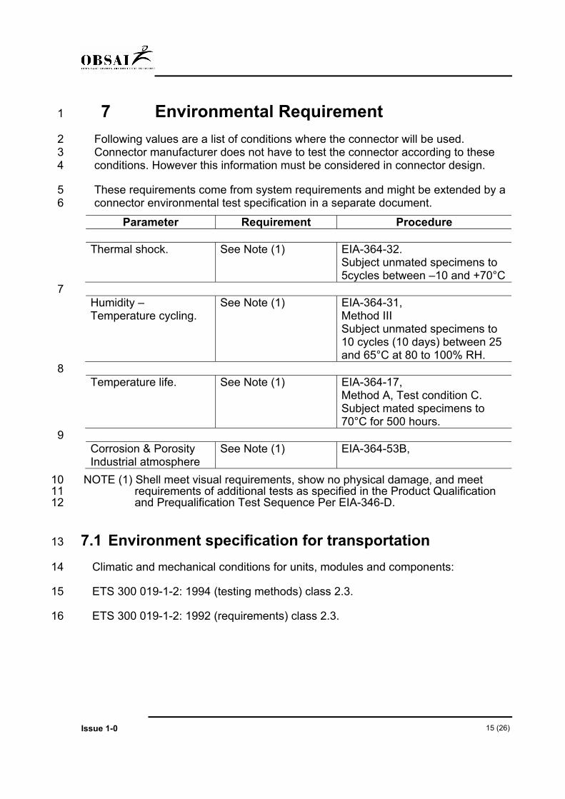
7 Environmental Requirement 1
Following values are a list of conditions where the connector will be used. 2 Connector manufacturer does not have to test the connector according to these 3 conditions. However this information must be considered in connector design. 4
These requirements come from system requirements and might be extended by a 5 connector environmental test specification in a separate document. 6
Parameter Requirement Procedure Thermal shock.
See Note (1) EIA-364-32. Subject unmated specimens to 5cycles between –10 and +70°C
7 Humidity – Temperature cycling.
See Note (1) EIA-364-31, Method III Subject unmated specimens to 10 cycles (10 days) between 25 and 65°C at 80 to 100% RH.
8 Temperature life.
See Note (1) EIA-364-17, Method A, Test condition C. Subject mated specimens to 70°C for 500 hours.
9 Corrosion & Porosity Industrial atmosphere
See Note (1) EIA-364-53B,
NOTE (1) Shell meet visual requirements, show no physical damage, and meet 10 requirements of additional tests as specified in the Product Qualification 11 and Prequalification Test Sequence Per EIA-346-D. 12
7.1 Environment specification for transportation 13
Climatic and mechanical conditions for units, modules and components: 14
ETS 300 019-1-2: 1994 (testing methods) class 2.3. 15
ETS 300 019-1-2: 1992 (requirements) class 2.3. 16

Issue 1-0 16 (26)
8 PCB Layout and Minimum Connector 1
Spacing 2
3 4
5 Figure 5: Board layout of R/A Receptacle 6
7

Issue 1-0 17 (26)
9 Panel Cut-Out 1
2
3
Figure 6: R/A Receptacle Recommended Panel Cutout 4
5
6
7
8
9
10
11

Issue 1-0 18 (26)
10 Panel Mounting Inserts 1
4.00
Ø 3.60 – 0.05
0.10 x 45°
FULL KNURL1.00
0.39 MM STRAIGHT KNURLING.
A A
Outside Ø 4.00
0.25 x 45°
Thru Tap M2.5 x 0.45
SECTION A-A
2
NOTES:1. MATERIALS: STAINLESS STEEL PER ASTM A-582 TYPE. 303 CONDITION A 4mm DIA.
2. DEBURR AND REMOVE SHARP EDGES.
3. FINISH: PASSIVARE PER QQ-P-35. 3
4
5
Figure 7: Panel Inserts for Jack Screws 6

Issue 1-0 19 (26)
11 Specification Drawings 1
LC
LC
MFG. LOGO
2
Figure 8: Right Angle Receptacle Connector – 16 Positions 3
4

Issue 1-0 20 (26)
A
A
6.5 REF
1 2
3
Figure 9: Plug Assembly 4 5
PLASTIC WASHER
RECEPTACLE
PLUG
D
PANEL
P.C.BD
SECTION D - D
6
Figure 10: Fully Mated Condition 7

Issue 1-0 21 (26)
12 Mating Dimensions 1
2
3
Figure 11: Right Angle Receptacle 4
5
6
7
8
9
10

Issue 1-0 22 (26)
1
2
Figure 12: Cable Plug 3

Issue 1-0 23 (26)
13 Cable Assembly Specifications 1
2
3 Figure 13: General Cable Assembly Drawing 4
Unless otherwise specified, herein after specifications refers to L=3m long! 5
13.1 Electrical Specifications: 6
13.1.1 Insertion Loss Lower Limit for L=3m Long, High Speed Cable 7 Assembly: 8
( )
⎪⎪⎩
⎪⎪⎨
⎧
≤<−⎟⎠⎞
⎜⎝⎛ −×−
≤<×−=
GHzffff
ffGHzff
dBSDD7
3;5
35
31.0;5
2100
0
0 9
10 Where: 11 f is given in (GHz) 12 f0 = 1.575 GHz 13
13.1.2 Insertion Loss Lower Limit for L=3m Long, Low Speed Cable 14 Assembly: 15
( )
⎪⎪⎩
⎪⎪⎨
⎧
≤<−≤<−
≤<−≤<−
=
GHzfGHzfGHzfGHzf
dBSDD
5.41.2;301.2525.0;21
525.02.0;82.001.0;5
21 16
17 Where: 18 f is given in (GHz) 19
Issue 1-0 24 (26)
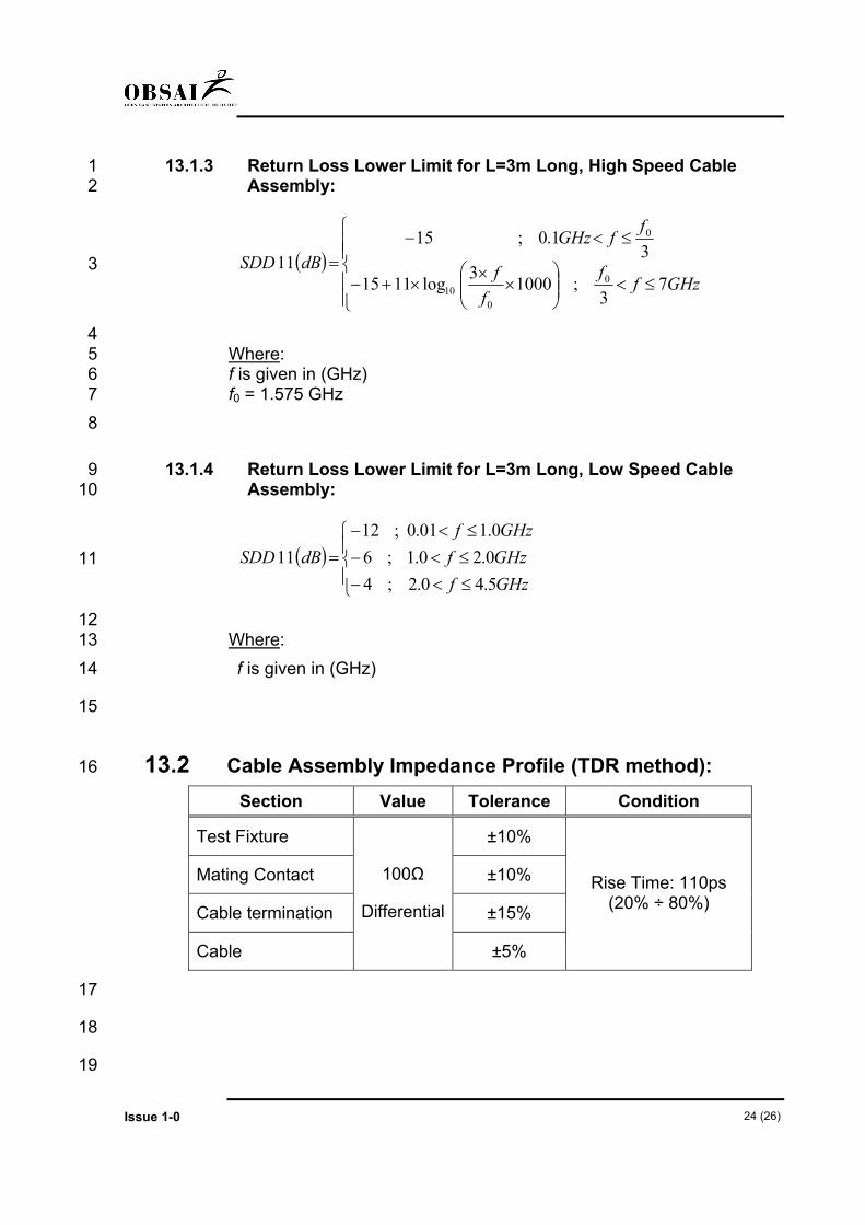
13.1.3 Return Loss Lower Limit for L=3m Long, High Speed Cable 1 Assembly: 2
( )
⎪⎪⎩
⎪⎪⎨
⎧
≤<⎟⎟⎠
⎞⎜⎜⎝
⎛×
××+−
≤<−=
GHzffff
ffGHzdBSDD
73
;10003log1115
31.0;15
110
010
0
3
4 Where: 5 f is given in (GHz) 6 f0 = 1.575 GHz 7
8
13.1.4 Return Loss Lower Limit for L=3m Long, Low Speed Cable 9 Assembly: 10
( )⎪⎩
⎪⎨
⎧
≤<−≤<−≤<−
=GHzfGHzfGHzf
dBSDD5.40.2;40.20.1;60.101.0;12
11 11
12 Where: 13 f is given in (GHz) 14
15
13.2 Cable Assembly Impedance Profile (TDR method): 16
Section Value Tolerance Condition
Test Fixture ±10%
Mating Contact ±10%
Cable termination ±15%
Cable
100Ω
Differential
±5%
Rise Time: 110ps (20% ÷ 80%)
17
18
19
Issue 1-0 25 (26)
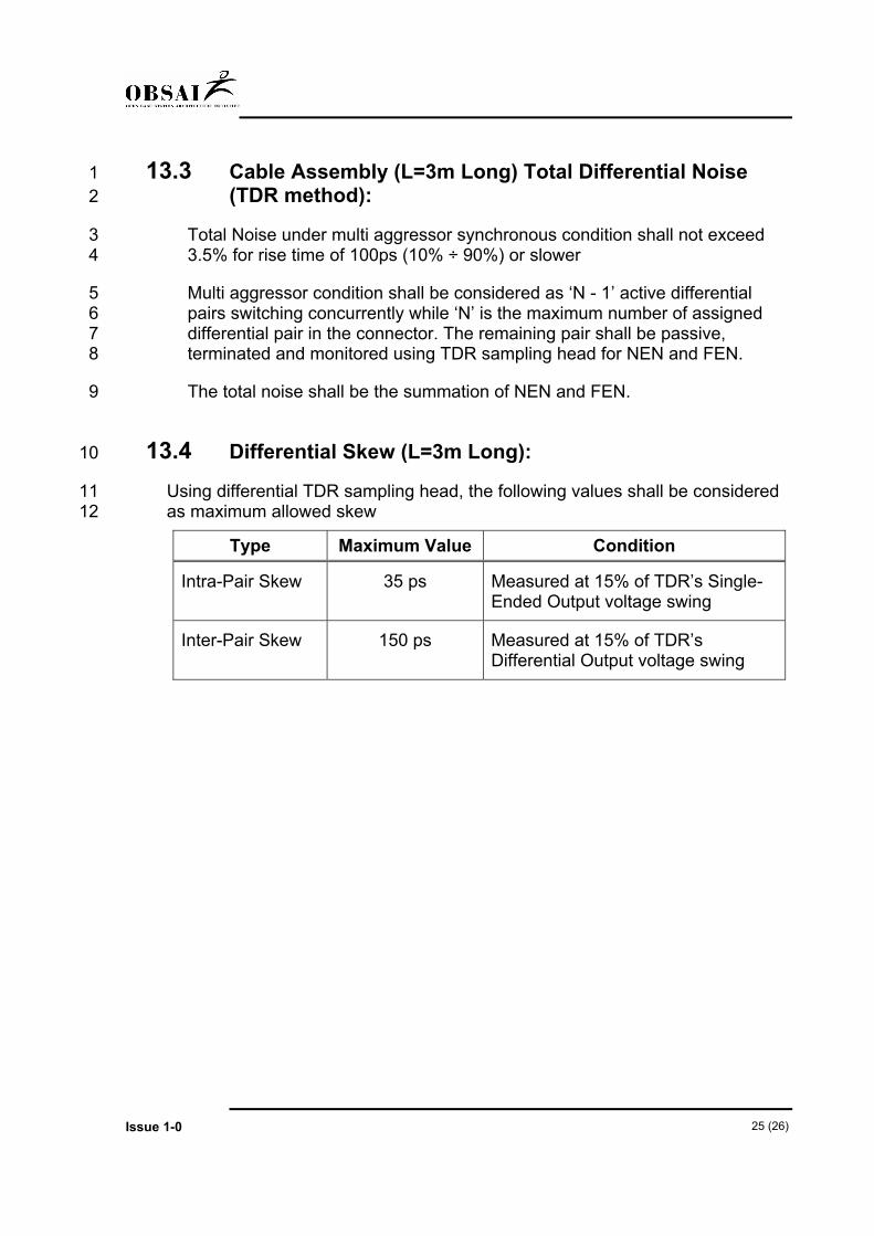
13.3 Cable Assembly (L=3m Long) Total Differential Noise 1 (TDR method): 2
Total Noise under multi aggressor synchronous condition shall not exceed 3 3.5% for rise time of 100ps (10% ÷ 90%) or slower 4
Multi aggressor condition shall be considered as ‘N - 1’ active differential 5 pairs switching concurrently while ‘N’ is the maximum number of assigned 6 differential pair in the connector. The remaining pair shall be passive, 7 terminated and monitored using TDR sampling head for NEN and FEN. 8
The total noise shall be the summation of NEN and FEN. 9
13.4 Differential Skew (L=3m Long): 10
Using differential TDR sampling head, the following values shall be considered 11 as maximum allowed skew 12
Type Maximum Value Condition
Intra-Pair Skew 35 ps Measured at 15% of TDR’s Single-Ended Output voltage swing
Inter-Pair Skew 150 ps Measured at 15% of TDR’s Differential Output voltage swing

Issue 1-0 26 (26)
14 Reference Documents 1
• MIL-STD-1344, test methods 2
• EIA-364 Test Procedures 3
• IEC-512 Test Procedures 4
• See EIA-364-D Annex Page A-1 to A-4 Test Comparison Cross Reference 5
(informative) among EIA-364, IEC-512 & MIL-STD-1344 6