Embed Size (px)
Citation preview

DATE :AUG.22.2003 TECHNICAL
SPECIFICATION
LCM
HY-1602F-801 Page 1 of 26
.
SHEN ZHEN AV-DISPLAY CO.,LTD
SPECIFICATIONS FOR
LIQUID CRYSTAL DISPLAY MODULE MODEL NO.: HY-1602F-801 DATE:AUG.22.2003
Approved Checked Department
CUSTOMER:
MODEL NO.: DATE:
Approved Checked Department
A

DATE :AUG.22.2003 TECHNICAL
SPECIFICATION
LCM
HY-1602F-801 Page 2 of 26
.
CONTENTS
Ⅰ. General Specification-------------------------------------------------------(3-6)
Ⅱ. The Characteristics and Reliability Test--------------------------------(7-8)
Ⅲ. The LCD Measuring Method and Equipment-------------------------(9-11)
Ⅳ. Standard Specifications for Product Quality-------------------------- (12-13)
Ⅴ. Instruction System and Description of Details------------------------(19-26)

DATE :AUG.22.2003 TECHNICAL
SPECIFICATION
LCM
HY-1602F-801 Page 3 of 26
.
Ⅰ.General Specifications
1. General
The AV-DISPLAY dot matrix LCD module consist of the liquid crystal display C-MOS driver and C-MOS LSI controller. the module utilizes 5*7 dot matrix characters to provide full alphanumeric capability. All control, refresh and display functions are executed by a dedicated on-board controller. the module is capable of displaying the full 160-character JIS font set .data interfacing is via the 4-bit or 8-bit bi-directional data bus by using of simple control commands the data can be selective written to the data register.
2. Features
A. Built-In Controller LSI.
B. 5*7 Dot Matrix With Cursor.
C. Micro-Processor Compatible Data-Bus Interface(4-Bit Or 8-Bit).
D. Character Generator ROM Built-In
5*8 Dot : ----------208 Character Fonts
5*10 Dot : ----------32 Character Fonts
E. Character Generator RAM--------Customer Rewritable
5*8 Font:8 Characters
F. Powerful Control Command
(1) Display Clear
(2) Return Home
(3) Cursor Preset
(4) Cursor On/Off Or Cursor Blinking
(5) Cursor Display Shift
(6) Display Shift
(7) Display On/Off Control
(8) Display Data Read/Write
G. Low power consumption 5.0v power supply

DATE :AUG.22.2003 TECHNICAL
SPECIFICATION
LCM
HY-1602F-801 Page 4 of 26
.
-20▲C ~ 70▲COperating Temperature5x8Character FontStorage TemperatureBlacklight
Ta= 25▲C, Vdd= 5.0V
DB0-DB7LEDALEDK
Symbol
R/W5
16
6
157-14
E
Supply Current
Dot Pitch (W*H)Dot Size (W*H)
Supply Current for Blacklight
Operating Voltage for LCDOperating Voltage
234
1Pin No
VDD
RSVo
VSS
Item
H/L
--
H/L--
H/H L
If
0.60x0.700.56x0.66
VddVddIdd
Symbol
Ta= 25▲C, Vf= 4.2V
--
H/L--
--Level
Test Condition
Ta= 25▲CTa= 25▲C
Register selection (H:Data registor, L:Instruction registor)Read/write selection (H:Read,L:Write)
Power supply for Blacklight(-)Power supply for Blacklight(+ )
Enable signal for chipData Bus line
5.0
2.04.5
30
Typ.
Power supply for Logic(+ 5.0)
Description
---
Power supply for LCD
GND
Min.
------
---
---
LED (White)-30▲C ~ 80▲C
Max.
---3.0
mA
Unit
VmA
V
Display Type
LCD ColourView Angle
Rear polarizer
LCD Type
or KS0066SPLC780A
CONTROL LSI
H. Attaching drawing and general description.
HY-1602F-801
Module Size (W*H*T)View Area (W*H)
Character Size(WxH)Character Pitch(W*H)
Item Nominal Dimensions(mm)
64.5x16.0
2.95x5.563.55x5.95
80.0x36.0x10.0
seg80
Backlight
com16
LCD Panel
3. 552. 96
0. 560. 6
LCD
FEATURE
MODULE
6 O'clockBULE MODE
TransmissiveNegative Type
STN
5.56
5.94 0.
66.7
16x2 CHARACTERS
1/16DUTY,1/5BIAS
1. 0
7. 3
MAX 10. 04- 2. 52.58
75. 0
1. 0
69. 2± 0. 2
2. 54*15=38. 1
64. 5( V. A)
16.0
(V.A
)
80. 0± 0. 3
31.0
24.2
±0.
2
1 16
36±
0.3

DATE :AUG.22.2003 TECHNICAL
SPECIFICATION
LCM
HY-1602F-801 Page 5 of 26
.
4.Timing Characteristics:
Write Operation and Read Operation Item Symbol Min. Typ. Max. Unit
Enable Cycle Time TCYCLE 500 -- -- nS
Enable Pulse Width PWEH 220 -- -- nS
Enable Rise & Fall Time TER,TEF -- -- 25 nS
Address Set-Up Time TAS 40 -- -- nS
Address Hold Time TAH 10 -- -- nS
Data Set-Up Time TDSW 60 -- -- nS
Data Hold Time TH 10 -- -- nS
Item Symbol Min. Typ. Max. Unit
Enable Cycle Time TCYCLE 500 -- -- nS
Enable Pulse Width PWEH 220 -- -- nS
Enable Rise & Fall Time TER,TEF - -- 25 nS
Address Set-Up Time TAS 40 -- -- nS
Address Hold Time TAH 10 -- -- nS
Data Set-Up Time TDSW - -- 120 nS
Data Hold Time TH 20 -- -- nS

DATE :AUG.22.2003 TECHNICAL
SPECIFICATION
LCM
HY-1602F-801 Page 6 of 26
.
5.Write Operation:
RS
R/W TAS TAH
TAH
PWEH
TEF
E TER
TDSW TH
DB0—DB7 Valid Data
TCYCLE
Read Operation
RS
R/W TAS TAH
TAH
PWEH
TEF
E TER
TDSW TH
DB0—DB7 Valid Data
TCYCLE

DATE :AUG.22.2003 TECHNICAL
SPECIFICATION
LCM
HY-1602F-801 Page 7 of 26
.
Ⅱ.The Characteristics and The Reliability Test
1.Electro-Optic Characteristics:
Condition:TEMP=(21±3)℃ HUM=(70±5)%RH
VDD: 5.0V FOSC: 270KHZ NO
Item Symbol Min. Typ. Max. Unit Remarks
1 Operating Voltage Vop 5.0 V 2 Current Consumption Is 1.30 mA
Ton 150 ms 3 Response Time Toff 120 ms
4 Contrast CR 3 12H θ1 15 6H θ2 45 3H θ3 50
5 Viewing Angle (CR≥3.0)
9H θ4 50
Deg.
6 Threshold Voltage Vth 1.14 V 7 Backlight Current
Consumption LED 30 mA

DATE :AUG.22.2003 TECHNICAL
SPECIFICATION
LCM
HY-1602F-801 Page 8 of 26
.
2.Reliability Test
No Items Test Condition Test Result
1
High Temp Storage
Temp:70±2℃ Time:96h Restore:24h
Passed
2
Low Temp Storage
Temp:-20±3℃ Time:96h Restore:24h
Passed
3
High Temp Static drive
Temp:50±2℃ Vop:5V Time:96h Restore:24h
Passed
4
Low Temp Static drive
Temp:0±3℃ Vop:5V Time:96h Restore:24h
Passed
5
High Temp High Hum Storage
Temp:40±2℃ Hum:95%Rh Time:96h Restore:24h
Passed
Temp:(℃) 70 25
-20 30 5 30 5 6
Thermal Shock
5 Cycles Restore:24h
Passed

DATE :AUG.22.2003 TECHNICAL
SPECIFICATION
LCM
HY-1602F-801 Page 9 of 26
.
Ⅲ.The LCD Measuring Method and Equipment
1. Current Consumption Measuring
(1) Equipment
DC
Power mA Supply CMOS IC
Waveform Generator F=64HZ A LCD B Sw
(2) Condition
Operating Frequency: 64HZ
Operating Voltage (RMS): Selected Voltage
2. Threshold Voltage and Response Time Measuring
(1) Equipment
L
30°
Oscilloscope
Waveform Generator

DATE :AUG.22.2003 TECHNICAL
SPECIFICATION
LCM
HY-1602F-801 Page 10 of 26
.
(2) Definition
A. Threshold Voltage (V ) th
Brightness
100%
80%
Nonselected Waveform
50% Selected Waveform
0 V V Drive Voltage sat th
B. Response Time
On
Off
90%
10% Time
T T r d

DATE :AUG.22.2003 TECHNICAL
SPECIFICATION
LCM
HY-1602F-801 Page 11 of 26
.
3. Contrast Measuring
(1) Equipment
L
30°
Oscilloscope
Waveform Generator
(2)Definition:
A.Viewing Angle:
Z
θ1 Y 12h,Φ=90°
9h,Ф=180 θ4 θ3 X 3h,Φ=0°
θ2
6h,Φ=270°
B. Contrast Ratio (Positive)
Brightness of non-selected wave-form CR= Brightness of selected wave-form

DATE :AUG.22.2003 TECHNICAL
SPECIFICATION
LCM
HY-1602F-801 Page 12 of 26
.
Ⅳ.Standard Specifications for Product Quality
1. Manner of Test:: 1.1.The Test Must Be Under 40w Flourescent Light, And The Distance Of View Must
Be At 30cm. 1.2.The Test Direction Is Based On Around 15°- 45° Of Vertical Line. 2. Definition Of Defects 2.1 Major Defects
A:Non-Display
B:Segment Missing
C:Over Current
D:Segment Short
E:Sealant Dishardexn
F:Wrong Polarizer Direction 2.2 Interface Circuit and Drive Programe on LCM of character series.
A. Interface circuit:
P1.3 DB3
P3.1P3.2
P1.6
P3.0P1.7
P1.5P1.4
DB6DB7
DB5DB4
P1.0
P1.2P1.1
DB0DB1DB2
RSERW
0—20k
VSS V0
B.Drive programme for testing LCM of character series.

DATE :AUG.22.2003 TECHNICAL
SPECIFICATION
LCM
HY-1602F-801 Page 13 of 26
.
ORG 0000H
AJMP MAIN
ORG 0300H
DB 58H,58H,58H,58H,58H,58H,58H,58H,
DB 58H,58H,58H,58H,58H,58H,58H,58H,
DB 58H,58H,58H,58H,58H,58H,58H,58H,
DB 58H,58H,58H,58H,58H,58H,58H,58H,
DB 58H,58H,58H,58H,58H,58H,58H,58H,
DB 58H,58H,58H,58H,58H,58H,58H,58H,
DB 58H,58H,58H,58H,58H,58H,58H,58H,
DB 58H,58H,58H,58H,58H,58H,58H,58H,
DB 58H,58H,58H,58H,58H,58H,58H,58H,
DB 58H,58H,58H,58H,58H,58H,58H,58H,
ORG 0350H
DB 2AH,59H,55H,53H,55H,4EH,47H,2AH,
DB 45H,4CH,45H,43H,2EH,4CH,54H,44H,
DB 2AH,44H,4FH,54H,2AH,4DH,41H,54H,
DB 52H,49H,58H,2AH,4CH,43H,44H,2AH,
DB 4BH,65H,5AH,6FH,6EH,48H,75H,69H,
DB 2AH,59H,55H,53H,55H,4EH,47H,2AH,
DB 45H,4CH,45H,43H,2EH,4CH,54H,44H,
DB 2AH,44H,4FH,54H,2AH,4DH,41H,54H,
DB 52H,49H,58H,2AH,4CH,43H,44H,2AH,
DB 4BH,65H,5AH,6FH,6EH,48H,75H,69H,
DB 2AH,2AH,2AH,2AH,2AH,2AH,2AH,2AH,
DB 44H,4FH,54H,20H,4DH,41H,54H,52H,
DB 49H,58H,20H,4CH,49H,51H,55H,49H,
DB 44H,20H,43H,52H,59H,53H,54H,41H,
DB 4CH,20H,44H,49H,53H,50H,4CH,41H,
DB 59H,20H,4DH,4FH,55H,44H,4CH,45H,
DB 2AH,2AH,2AH,2AH,2AH,2AH,2AH,2AH,
DB 2AH,2AH,2AH,2AH,2AH,2AH,2AH,2AH,

DATE :AUG.22.2003 TECHNICAL
SPECIFICATION
LCM
HY-1602F-801 Page 14 of 26
.
DB 54H,4DH,0B0H,44H,4DH,43H,34H,30H,
DB 32H,2AH,2AH,2AH,2AH,2AH,2AH,2AH,
DB 2AH,2AH,2AH,2AH,2AH,2AH,2AH,2AH,
DB 2AH,2AH,2AH,2AH,2AH,2AH,2AH,2AH,
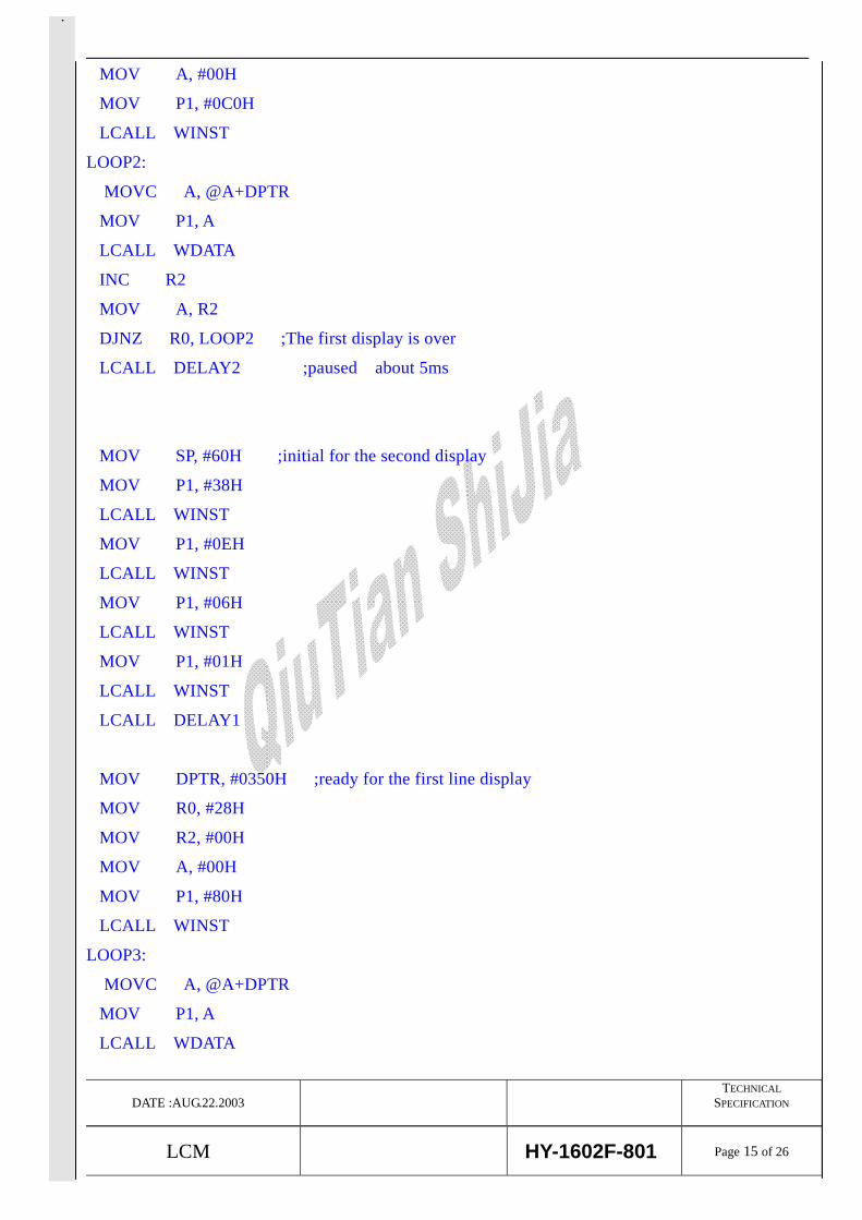
MAIN :
MOV SP, #60H ;Initial for the first display
MOV P1, #38H ;set function
LCALL WINST
MOV P1, #0EH ;set display on/off control
LCALL WINST
MOV P1, #06H ;set Entry mode
LCALL WINST
MOV P1, #01H ;clear display,write code 20h into all DDRAM
LCALL WINST
LCALL DELAY1
MOV DPTR, #0300H
MOV R0, #28H ;Set Pointer
MOV R2, #00H
MOV A, #00H
MOV P1, #80H ;set DDRAM address 0000h
LCALL WINST
LOOP1:
MOVC A, @A+DPTR
MOV P1, A
LCALL WDATA
INC R2
MOV A, R2
DJNZ R0, LOOP1
MOV DPTR, #0328H
MOV R0, #28H
MOV R2, #00H
DATE :AUG.22.2003 TECHNICAL
SPECIFICATION
LCM
HY-1602F-801 Page 15 of 26
.
MOV A, #00H
MOV P1, #0C0H
LCALL WINST
LOOP2:
MOVC A, @A+DPTR
MOV P1, A
LCALL WDATA
INC R2
MOV A, R2
DJNZ R0, LOOP2 ;The first display is over
LCALL DELAY2 ;paused about 5ms
MOV SP, #60H ;initial for the second display
MOV P1, #38H
LCALL WINST
MOV P1, #0EH
LCALL WINST
MOV P1, #06H
LCALL WINST
MOV P1, #01H
LCALL WINST
LCALL DELAY1
MOV DPTR, #0350H ;ready for the first line display
MOV R0, #28H
MOV R2, #00H
MOV A, #00H
MOV P1, #80H
LCALL WINST
LOOP3:
MOVC A, @A+DPTR
MOV P1, A
LCALL WDATA

DATE :AUG.22.2003 TECHNICAL
SPECIFICATION
LCM
HY-1602F-801 Page 16 of 26
.
INC R2
MOV A, R2
DJNZ R0, LOOP3 ;THE first line display is over
MOV DPTR, #0378H ;ready for the second line display
MOV R0, #28H
MOV R2, #00H
MOV A, #00H
MOV P1, #0C0H
LCALL WINST
LOOP4:
MOVC A, @A+DPTR
MOV P1, A
LCALL WDATA
INC R2
MOV A, R2
DJNZ R0, LOOP4 ;main program is end upto here
LOOP5:
LCALL DELAY2
AJMP MAIN
WINST:
CLR P3.0 ;write to instruction register
CLR P3.2
SETB P3.1
LCALL DELAY1
CLR P3.1
LCALL DELAY1
RET
WDATA:
CLR P3.2 ;write to data register
SETB P3.0
SETB P3.1

DATE :AUG.22.2003 TECHNICAL
SPECIFICATION
LCM
HY-1602F-801 Page 17 of 26
.
LCALL DELAY1
CLR P3.1
LCALL DELAY1
RET
DELAY1:
MOV 50H, #08H ;delay 1648 us
ADDR1: PUSH 50H
ADDR2: PUSH 50H
ADDR3: PUSH 50H
ADDR4: DJNZ 50H, ADDR4
POP 50H
DJNZ 50H, ADDR3
POP 50H
DJNZ 50H, ADDR2
POP 50H
DJNZ 50H, ADDR1
RET
DELAY2:
MOV R0, #0CCH
MOV R2, #66H
ADDR5:
LCALL DELAY1 ;delay ccH X 1648us
DJNZ R0, ADDR5
ADDR6:
LCALL DELAY1 ;delay 66H X 1648us total 5.05ms
DJNZ R2, ADDR6
RET
END

DATE :AUG.22.2003 TECHNICAL
SPECIFICATION
LCM
HY-1602F-801 Page 18 of 26
.
3.Inspection Item and Standards
Item The Standard Of Quality Inspection Checking
Manner Quality Ratio
Frame
Smooth and even surface,no crack,no scratch,no rusty,and not be wrenched out of shape.the range between convex and concave is:d≤0.35mm,and the frame must be connected to the ground.
Checking With Eyes And Using Vernier Caliper, Multimeter
100%
LCD The major defects would be reject.no scratch and no dusty on the LCD glass surface.d≤0.15mm n≤2 diameter of bubble:d≤0.5 n≤2 damaged size of polarizer:d≤0.15mm, n≤2.
Check It When Displaying
100%
The Relative Position of LCD and Frame
The sealant mouth of the LCD must be at the same side with the frame’s.
Checking With Eyes
100%
The Relative Position of
PCB Paneland
Frame
The frame installing direction must be correct.the twisted angle of the pin is from 45°to 60°,the pin is vertical to PCB panel and it must be in the middle position of the installing holes.
Checking With Eyes
100%
Function Test
1. The major defects must be reject. 2. Test flow chart (see attached chart) 3. Background changes evenly and no
disorderly displaying phenomenon. 4. Display no shortage.
Check It When Displaying
100%
Note:D~Diameter N~Quantity Unit:mm

DATE :AUG.22.2003 TECHNICAL
SPECIFICATION
LCM
HY-1602F-801 Page 19 of 26
.
Ⅴ.Instruction System and Description of Details
1.Instruction System Only two SPLC780A OR S6A0069X01-C0CX registers,the Instruction Register (IR) and
the Data Register (DR) can be directly controlled by the MPU.Prior to internal operation
start,control information is temporarily stored in these registers,to allow interface form
SPLC780A OR S6A0069X01-C0CX internal operation to various types of MPUs which
operate in different speeds or to allow interface to peripheral control ICS.SPLC780A OR
S6A0069X01-C0CX internal operation is determined by signals sent from the MPU.These
signals include register selection signal(RS),read/write signals (R/W) and data bus
signals (DB0―DB7),and are called instructions,here.Table 1 shows the instructions and
their execution time.Details are explained in subsequent sections.
Instructions are of 4 types, those that,
(1) Designate SPLC780A OR S6A0069X01-C0CX functions such as display format,data
length,etc.
(2) Give internal RAM addresses.
(3) Perform data transfer with internal RAM.
(4) Others.
In normal use,category (3) instructions are used most frequently.However,automatic in-
crementing by +1 (or decrementing by –1) of SPLC780A OR S6A0069X01-C0CX internal
RAM addresses after each data write lessens the MPU program load.The display shift is
especially able to perform concurrently with display data write ,enabling the user to
develop systems in minimum time with maximum programming efficiency.For an
explanation of the shift function in its relation to display ,.When an instruction is executing
during internal operation,no instruction other than the busy flag/address read instruction
will be executed.
Because the busy flag is set to “1” while an instruction is being executed,check to make
sure it is on “1” before sending an instruction from the MPU.
Note 1
Make sure the SPLC780A OR S6A0069X01-C0CX is not in the busy state (BF=0)
before sending the instruction from the MPU to the SPLC780A OR S6A0069X01-C0CX. If
the instruction is sent without checking the busy flag the time between first and next
instructions is much longer than the instruction time.
See Table 1 for a list of each instruction execution time.
Note 2
After executing instruction of writing data to CG/DD RAM or reading data from CG/
DATE :AUG.22.2003 TECHNICAL
SPECIFICATION
LCM
HY-1602F-801 Page 20 of 26
.
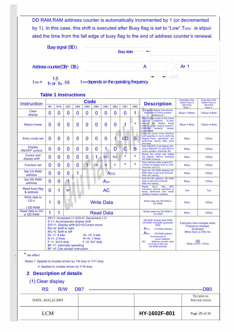
DD RAM,RAM address counter is automatically incremented by 1 (or decremented
by 1). In this case, this shift is executed after Busy flag is set to “Low”.TADD is stipul-
ated the time from the fall edge of busy flag to the end of address counter’s renewal.
Busy signal (BD )
Address counter(DB DB )
Busy state
~0 7 A A+ 1
t depends on the operating frequencyADDt = (s)ADD1.5
fCP or fOSC
Table 1 Instructions
Code Execution time (when Fose is
250 KHz) Note 1
Execution time (when Fose is
160 KHz) Note 2
Instruction Description R/W DB6 DB5 RS DB7 DB4 DB3 DB2 DB1 DB0
Clears all display and returns theCursor to home position
(Address 0). Clear 0 0 0 0 0 0 0 0 0 1display 82us~1.64ms 120us~4.9ms
Return home 0 0 0 0 0 0 0 0 1 * Returns the cursor to the home position (Address 0).Also returns the display being shifted to the original position. DDRAM contents remain unchanged.
40us~1.6ms 120us~4.8ms
Sets the cursor move direction and specifies or not to shift the display.These operations are performed during data write and read
Entry mode set 0 0 0 0 0 0 0 1 I/D S 40us 120us
Sets ON/OFF of all display (D), Display ON/OFF control 0 0 0 0 0 0 1 D C B cursor ON/OFF (C),and blink f o
cursor position character (B). 40us 120us
Cursor and display shift 0 0 0 0 0 1 S/C R/L * *
Moves the cursor and shites the display without changing DD RAM contents. 40us 120us
Function set 0 0 0 0 1 DL N F * * Sets interface data length (DL) number of display nes (L) and licharacter font (F). 40us 120us
Sets the CG RAM address.CG RAM data is sent nd received Set CG RAM
address ACG 0 0 0 1 aAfter this setting . 40us 120us
Sets the DD address. DD RAM data is sent and r ived Set DD RAM
address ADD 0 0 1 eceAfter this setting . 40us 120us
Reads Busy flag (BF) indicating internal operation is being performed and reads address counter contents.
Read busy flag & address AC 0 1 BF 1us 1us
Write data to CG o 1 0 Write Data Writes data into DD RAM or
CG RAM. 40us 120us r DD RAM
Read data to CG or DD RAM 1 1 Read Data Reads data from DD RAM or
CG RAM 40us 120us
I/D=1: Increment (+1)I/D=0: Decrement (-1) DD RAM: Display data RAM S =1: Accompanies display shift CG RAM: Character generator Execution time changes when S/C=1: Display shift S/C=0:Cursor move RAM Frequency changes. ACG: CG RAM address R/L=0: Shift to right (Example)
R/L=0: Shift to left When fosc is 270k Hz: ADD: DD RAM address DL =1: 8 bits DL =0: 4 bits Corresponds to N =1: 2 lines N =0: 1 lines cursor address
250F =1: 5x10 dots F =0: 5x7 dots BF =1: Internally operating BF =0: Can accept instruction
AC: Address counter used 40us x 270 = 37us For both of DD and
CG RAM address
L * No effect
Notes 1: Applied to models driven by 1/8 duty or 1/11 duty.
2: Applied to models driven by 1/16 duty. 2. Description of details
(1) Clear display
RS R/W DB7 ----------------------------------------------------------------------DB0

DATE :AUG.22.2003 TECHNICAL
SPECIFICATION
LCM
HY-1602F-801 Page 21 of 26
.
Code 0 0 0 0 0 0 0 0 0 1
Writes space code “20” (hexadecimal) (character pattern for character code “20”
must be blank pattern) into all DD RAM address.Set DD RAM address 0 in address
counter.Returns display to its original status if it was shifted. In other words.the dis-
play disappears and the cursor or blink go to the left edge of the display (the first
if 2 lines are displayer).Set I/D= 1 (Increment Mode) of Entry Mode.S of Entry Mode
doesn’t change.
(2) Return home
RS R/W DB7 ----------------------------------------------------------------------DB0 Code 0 0 0 0 0 0 0 0 1 *
*No effect
Sets the DD RAM address 0 in address counter. Returns display to its original
status if it was shifted. DD RAM contents do not change. The cursor or blink go to
the left edge of the display (the first line if 2 lines are displayed).
(3) Entry mode set
RS R/W DB7 ----------------------------------------------------------------------DB0 Code 1 I/D S 0 0 0 0 0 0 0
I/D: Increments (I/D = 1) or decrement s (I/D) the DD RAM address by 1 when a
character code is written into or read from the DD RAM .The cursor blink moves
to the right when incremented by 1 and to the left when decremented by 1. The
same applies to writing and reading of CG RAM.
S: Shifts the entire display either to the right or to the left when S is 1; to the left
when I/D = 1 and to the right when I/D = 0. Thus it looks as if the cursor stands still
and the display moves.The display does not shift when reading from the DD RAM
when writing into or reading out from the CG RAM does it shift when S =0.
(4) Display ON/OFF control
RS R/W DB7 ----------------------------------------------------------------------DB0
Code 0 0 0 0 0 0 1 D C B
D: The display is ON when D = 1 and OFF when D = 0. when off due to D = 0,display
Data remains in the DD RAM.It can be displayed immediately by setting D = 1.
C: The cursor displays when C = 1 and does not display when C = 0. Even if the
Cursor disappears,the function of I/D,etc.does not change during display data
write.
The cursor is displayed using 5 dots in the 8th line when the 5x7 dot character font

DATE :AUG.22.2003 TECHNICAL
SPECIFICATION
LCM
HY-1602F-801 Page 22 of 26
.
Is selected and 5 dots in the 11th line when the 5x10 dot character font is selected.
B: The character indicated by the cursor blink when B = 1.The blink is displayed by
Switching between all blank dots and display characters at 409.6 ms interval when
fcp or fosc =250Khz. The cursor and the blink can be set to display simultaneously.
(The blink frequency changes according to the reciprocal of fcp or fose. 409.6x250/
270 = 379.2ms when fcp = 270kHz).
Cursor
5x7 dot character font 5x10 dot character font Alternating display
(a) Cursor Display Example (b) Blink Display Example
(5) Cursor or display shift
RS R/W DB7 ----------------------------------------------------------------------DB0 Code 0 0 0 0 0 1 S/c R/l * *
*No effect
Shifts Cursor position or display to the right or left without writing or reading display
data.This function is used to correct or search for the display .In a 2-lines display,
the cursor moves to the 2nd line when its passes the 40th digit of the 1st line.Notice
that the 1st and 2nd line display will shift at the same time.When the displayed data
is shifted repeatedly each line only moves horizontally.The 2nd line display does not
shift into the 1st line position
S/C R/L 0 0 Shifts the cursor position to the left.(AC is decremented by one.)
0 1 Shifts the cursor position to the right. (AC is decremented by one.)
1 0 Shifts the entire display to the left. The cursor follows the display shift.
2 1 Shifts the entire display to the right.The cursor follows the display shift.
Address counter (AC) contents do not change if the only action performed is shift
(6) Function set
RS R/W DB7 ----------------------------------------------------------------------DB0 Code 0 0 0 0 1 DL N F * *
*No effect
DL: Sets interface data length.Data is sent or received in 8 bit lengths (DB7~DB0) when
DL = 1and in 4 bit lengths (DB7~DB4) when DL = 0.when the 4 bit length is selected

DATE :AUG.22.2003 TECHNICAL
SPECIFICATION
LCM
HY-1602F-801 Page 23 of 26
.
Data must be sent or received twice.
N: Sets number of display lines
F: Sets character font. (Note) Perform the function at the head of the program before executing all instruction
(expect “Busy flag/address read”).From this point,the function set instruction
cannot be executed unless the interface data length is changed. N F No.of display lines Character font Duty factor Remarks 0 0 1 5x7 dots 1/8 0 1 1 5x10 dots 1/11
1 * 2 5x7 dots 1/16 Cannot display 2 lines with 5x10 dot character font.
*No effect
(7) Set CG RAM address RS R/W DB7 ----------------------------------------------------------------------DB0
Code 0 0 0 1 A A A A A A
←Higher Order Bits Lower Order Bits→
Sets the CG RAM address into the address counter in binary AAAAAA.Data is then
Written or read from the MPU for the CG RAM
(8) Set DD RAM address RS R/W DB7 ----------------------------------------------------------------------DB0
Code 0 0 1 A A A A A A A
←Higher Order Bits Lower Order Bits→
Sets the DD RAM address into the address counter in binary AAAAAAA.Data is
then Written or read from the MPU for the DD RAM.
However, When N = 0 (1-line display),AAAAAAA is “00” ~ “4F” (hexadecimal).
When N = 1 (2-line display),AAAAAAA is “00” ~ “27” (hexadecimal) for
the first line,and “40” ~ “67” (hexadecimal) for the second line.
(9) Read busy flag & address RS R/W DB7 ----------------------------------------------------------------------DB0
Code 0 1 BF A A A A A A A
←Higher Order Bits Lower Order Bits→
Reads the busy flag (BF) that indicates the system is now internally operating by a
previously received instruction.BF=1 indicates that internal operation is in progress.
The next instruction will not be accepted until BF is set to “0”.check the BF status
before the next write operation.At the same time,the value of the address counter
expressed in binary AAAAAAA is read out. The address counter is used by both CG

DATE :AUG.22.2003 TECHNICAL
SPECIFICATION
LCM
HY-1602F-801 Page 24 of 26
.
and DD RAM address ,and its value is determined by the previous instruction.
Address contents are the same as in terms (7) and (8).
(10) Write data to CG or DD RAM
RS R/W DB7 ----------------------------------------------------------------------DB0 Code 1 0 D D D D D D D D
←Higher Order Bits Lower Order Bits→
Writes binary 8 bit data DDDDDDDD to the CG or the DD RAM.Whether the CG or
DD RAM is to be written into is determined by the previous specification of CG RAM
or DD RAM address setting .After write ,the address is automatically incremented or
decremented by 1 according to entry mode.The entry mode also determines display
shift.
(11) Read data from CG or DD RAM RS R/W DB7 ----------------------------------------------------------------------DB0
Code 1 1 D D D D D D D D
←Higher Order Bits Lower Order Bits→
Reads binary 8 bits data DDDDDDDD from the CG or DD RAM. The previous desi-
gnation determines whether the CG or DD RAM is to be read. Before entering the
read instruction ,you must execute either the CG RAM or DD RAM address set
instruction.If you don’t,the first read data will be invalidated. When serially executing
the “read” instruction,the next address data is normally read from the second read.
The “address set” instruction need not be executed just before the “read” instruction
when shifting the cursor by cursor shift instruction (when reading out DD RAM).The
cursor shift instruction operation is the same as that of the DD RAM ‘s address set
instruction.
After a read, the entry mode automatically increases or decreases the address by 1.
However, display shift is not executed no matter what the entry mode is.
(Note) The address counter (AC) is automatically incremented or decremented by 1
after”write”instructions to either CG RAM or DD RAM. RAM data selected by the
AC cannot than be read out even if “read” instructions are executed. The conditions
for correct data read out are : execute either the address set instruction or cursor
shift instruction (only with DD RAM), just before reading out execute the “read” inst-
ruction from the second time the “read” instruction is serial.

DATE :AUG.22.2003 TECHNICAL
SPECIFICATION
LCM
HY-1602F-801 Page 25 of 26
.
3 . Precaution on programming
(1) Instruction of function set Perform the function at the head of program that accesses SPLC780A OR
S6A0069X01-C0CX before executing all instructions,and not change the data of the
instruction Register in the program. The data of function register can be changed by
the program as follow;
a.·Changing of DL (Data Length)
·when DL is changed from 8-bit length mode.
·when DL is changed from 4-bit length mode.
b.·Changing of N (Column Number)
·Perform the instruction of function set after executing instruction of display
clear or display off.
In this case, sequence of AC and DD RAM must be changed.Thus, rewrite the
address set register after that.
c.·Changing of F (Font)
·There is no problem in this case, but for dual-line display,the font mode of 5x11
cannot be selected (this mode is forbidden by hardware).
When N of F is changed, power supply voltage for LCD must be changed.If not
Changed,crosstalk will appear,or contrast will be poor.
(2) Busy flag check
SPLC780A OR KS0066 is produced in the CMOS process,therefore internal
executing time is long.
Standard time is 40us~1.6ms. (This varies by instruction).
When the high speed MPU controls it, check the busy flag before performing
Instruction or reading data.
While internal operation is active, Enable signal is not accepted. (Enable signal at
Reading status register for checking busy flag is accepted) Busy flag signal is
output through DB7, as shown in Table 3, when RS = “0”,R/W = “1 “,and Enable=”1”
(3) Iuput of unidentified instruction code Undefined instruction code of SPLC780A OR S6A0069X01-C0CX is only as follows;
RS R/W DB7~DB
0 0 0~
(Others are included to defined instruction)
When the undefined instruction code is loaded to SPLC780A OR

DATE :AUG.22.2003 TECHNICAL
SPECIFICATION
LCM
HY-1602F-801 Page 26 of 26
.
S6A0069X01-C0CX, it accepts the code,but Does not change the internal states
(RAM and other status of Flags). Busy state,
However continues for maximum 40us by the acceptance of the code.
Table 2 The relation between the operation and the combination of RS,R/W RS R/W E Operation 0 0 ¯¯↘__ Write instruction code 0 1 __╱¯¯╲__ Read busy flag and address counter1 0 ¯¯↘__ Write data 1 1 __╱¯¯╲__ Read data
When performing data and instruction code by 4 bit, transfer RS, R/W every time.