Embed Size (px)
Citation preview
SPECIFICATION FOR
LCM MODULE
MODULE NO.: CGG128032I01-FIN-R DOC.REVISION:00
Customer Approval:
SIGNATURE DATE
PREPARED BY (RD ENGINEER)
PREPARED BY (QA ENGINEER)
CHECKED BY
APPROVED BY

DOCUMENT REVISION HISTORY Version DATE DESCRIPTION CHANGED
BY 00 Oct-27-2010 First issue

CONTENTS 1. Functions & Features 2 2. Mechanical specifications 2 3. Block diagram 2 4. Dimensional outline 3 5. LCD driving voltage generator and bias reference circuit 4 6. Pin description 5 7. Maximum absolute limit 6 8. Electrical characteristics 7-8 9. Timing characteristics 8-9 10. Control and display command 10 11. Electro-Optical characteristics 11 12. Precaution for using LCD/LCM 12~13 13. LCM test criteria 14~22

2
1. FUNCTIONS & FEATURES 1.1. Format : 128x32 Dots 1.2. LCD mode : FSTN/Positive/Transmissive 1.3. Viewing direction : 6 o’clock 1.4. Driving scheme : 1/33 Duty cycle, 1/6 Bias 1.5. Power supply voltage (VDD) : 3.3V 1.6. LCD driving voltage (VLCD) : 6.5V(Reference voltage) 1.7. Operation temp :-20~70℃ 1.8. Storage temp : -30~80℃ 1.9. RoHS compliant.
2. MECHANICAL SPECIFICATIONS 2.1. Module size : 65.0mm(L)*29.5mm(W)*2.95mm(H) (Excluding Lcd Pin length 7.0mm) 2.2. Viewing area : 62.0mm(L)*20.5mm(W) 2.3. Dot pitch : 0.44mm(L)*0.54mm(W) 2.4. Dot size : 0.40mm(L)*0.50mm(W) 2.5. Weight : Approx. 3. BLOCK DIAGRAM
Figure 1.Block diagram

3
4. DIMENSIONAL OUTLINE
模
组
型
号M
OD
UL
E N
UM
BE
R
DO
NO
T S
CA
LE
TH
IS D
RA
WIN
G.
零 件
编 码
PA
RT
NO
:P
RO
JEC
TIO
N三
角
法
UN
IT 单
位
DA
TE
日 期
mm
AP
PR
OV
AL
S
DW
N:
比 例
页 次
SHE
ET
:
GE
NE
RA
L T
OL
:
SCA
LE
:
未
注
公
差
签 字
AP
P:
CH
K:
FIT
适
应图面
±0.
3
1O
F1
RE
V 版
本
AD
ESC
RIP
TIO
N 描
述
Fir
st is
sue
DA
TE
日期
Aug
-12-
2010
CG
G12
8032
I01-
FIN
-RC
GG
1280
32I0
1-FI
N-R
Figure2. Dimensional outline


4
5. LCD DRIVING VOLTAGE GENERATOR AND BIAS REFERENCE CIRCUIT
NOTE: Reference circuit used 4 times booster circuit .
■Recommended component values:C1: 1.0 to 4.7uF;C2: 0.47~1.0uF ■C1,C2 is determined by the size of the LCD being driven. Select a value that will stabilize the liquid crystal drive
voltage. ■ Ra and Rb maybe changed in mass productions to keep the consistency of display contrast.

5
6. PIN DESCRIPTION
No. Symbol Function
1-5 V0-V4 LCD driver supplies voltages.
6 VSS Power ground (0V)
7-11 CAP2N,CAP2P,CAP
1P,CAP1N,CAP3P, Capacitor 2-/2+/1+/1-/3+ pad for internal DC/DC voltage converter
12 VOUT DC/DC voltage converter output
13 VSS Power ground (0V)
14 VDD2 Power supply
15 VDD Power supply for LCM (+3.3V)
16 SI Serial data input
17 SCL Serial clock input
18 A0 This is connected to the least significant bit of the normal MPU address bus, and it determines whether the data bits are data or a command
19 RST When /REST is set to “L”, the settings are initialized The reset operation is performed by the /REST signal level
20 CS1B This is the chip select signal(When CS1=L then the chip select
become active)

6
7. MAXIMUM ABSOUTE LIMIT Maximum Ratings (Voltage Reference to VSS)(for IC)

7
8. ELECTRICAL CHARACTERISTICS DC CHARACTERISTICS

8
9. TIMING CHARACTERISTICS
9
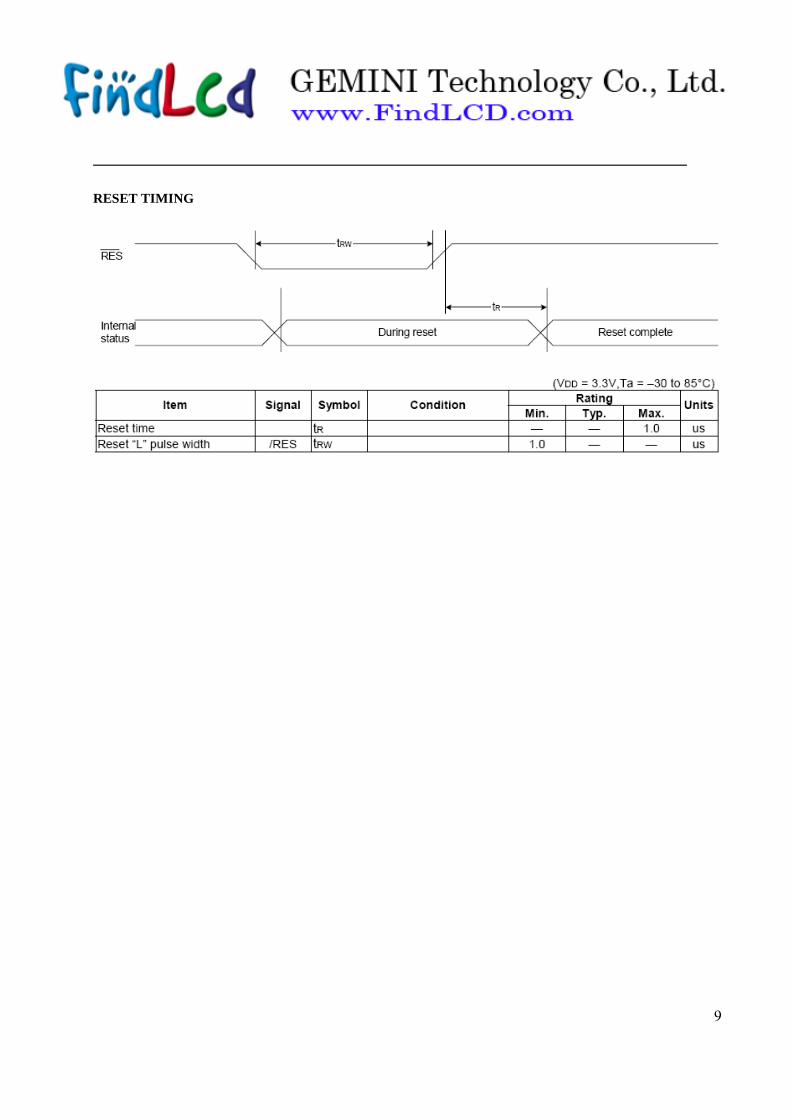
RESET TIMING

10
10. CONTROL AND DISPLAY INSTRUCTION

11
11. ELECTRO-OPTICAL CHARACTERISTICS (VDD = 3.3V, Ta = 25°C)
Item Symbol Condition Min Typ Max Unit Ta =-20°C 6.8 7.0 7.2 Ta = 25°C 6.3 6.5 6.7 Operating Voltage
for LCD
Vop
Ta = 70°C 5.8 6.0 6.2 V
Tr --- 250 500 ms Response time Tf Ta = 25°C --- 300 600 ms Contrast Cr Ta = 25°C 2 4 --- ---
θ -35 --- +35 deg Viewing angle range
Ф Cr≥2 -35 --- +40 deg

12
12. PRECAUTION FOR USING LCD/LCM
After reliability test, recovery time should be 24 hours minimum. Moreover, functions,
performance and appearance shall be free from remarkable deterioration within 50,000 hours
(average) under ordinary operating and storage conditions room temperature (20+8°C), normal
humidity (below 65% RH), and in the area not exposed to direct sun light. Using LCM beyond these
conditions will shorten the life time.
Precaution for using LCD/LCM
LCD/LCM is assembled and adjusted with a high degree of precision. Do not attempt to make any
alteration or modification. The followings should be noted.
General Precautions:
1. LCD panel is made of glass. Avoid excessive mechanical shock or applying strong pressure onto the surface of display area.
2. The polarizer used on the display surface is easily scratched and damaged. Extreme care should be taken when handling. To clean dust or dirt off the display surface, wipe gently with cotton, or other soft material soaked with isoproply alcohol, ethyl alcohol or trichlorotriflorothane, do not use water, ketone or aromatics and never scrub hard.
3. Do not tamper in any way with the tabs on the metal frame.
4. Do not make any modification on the PCB without consulting Gemini.
5. When mounting a LCM, make sure that the PCB is not under any stress such as bending or
twisting. Elastomer contacts are very delicate and missing pixels could result from slight
dislocation of any of the elements.
6. Avoid pressing on the metal bezel, otherwise the elastomer connector could be deformed and
lose contact, resulting in missing pixels and also cause rainbow on the display.
7. Be careful not to touch or swallow liquid crystal that might leak from a damaged cell. Any liquid crystal adheres to skin or clothes, wash it off immediately with soap and water.
Static Electricity Precautions:
1. CMOS-LSI is used for the module circuit; therefore operators should be grounded whenever he/she comes into contact with the module.
2. Do not touch any of the conductive parts such as the LSI pads; the copper leads on the PCB and the interface terminals with any parts of the human body.
3. Do not touch the connection terminals of the display with bare hand; it will cause disconnection or defective insulation of terminals.
13
4. The modules should be kept in anti-static bags or other containers resistant to static for storage. 5. Only properly grounded soldering irons should be used. 6. If an electric screwdriver is used, it should be grounded and shielded to prevent sparks. 7. The normal static prevention measures should be observed for work clothes and working
benches. 8. Since dry air is inductive to static, a relative humidity of 50-60% is recommended. Soldering Precautions:
1. Soldering should be performed only on the I/O terminals. 2. Use soldering irons with proper grounding and no leakage. 3. Soldering temperature: 350°C+10°C 4. Soldering time: 3 to 4 second. 5. Use eutectic solder with resin flux filling. 6. If flux is used, the LCD surface should be protected to avoid spattering flux. 7. Flux residue should be removed. Operation Precautions:
1. The viewing angle can be adjusted by varying the LCD driving voltage Vo. 2. Since applied DC voltage causes electro-chemical reactions, which deteriorate the display, the
applied pulse waveform should be a symmetric waveform such that no DC component remains. Be sure to use the specified operating voltage.
3. Driving voltage should be kept within specified range; excess voltage will shorten display life. 4. Response time increases with decrease in temperature. 5. Display color may be affected at temperatures above its operational range. 6. Keep the temperature within the specified range usage and storage. Excessive temperature and humidity could cause polarization degradation, polarizer peel-off or generate bubbles. 7. For long-term storage over 40°C is required, the relative humidity should be kept below 60%, and avoid direct sunlight. Limited Warranty
Gemini LCDs and modules are not consumer products, but may be incorporated by Gemini’s customers into consumer products or components thereof, Gemini does not warrant that its LCDs and components are fit for any such particular purpose. 1. The liability of Gemini is limited to repair or replacement on the terms set forth below. Gemini will not
be responsible for any subsequent or consequential events or injury or damage to any personnel or user including third party personnel and/or user. Unless otherwise agreed in writing between Gemini and the customer, Gemini will only replace or repair any of its LCD which is found defective electrically or visually when inspected in accordance with Gemini general LCD inspection standard . (Copies available on request)
2. No warranty can be granted if any of the precautions state in handling liquid crystal display above has been disregarded. Broken glass, scratches on polarizer mechanical damages as well as defects that are caused accelerated environment tests are excluded from warranty.
3. In returning the LCD/LCM, they must be properly packaged; there should be detailed description of the failures or defect.

14
13. LCM test criteria 1.Objective
The LCM test criteria are set to formalize Gemini’s LCM quality standards with reference to those of the customer for inspection, release and acceptance of finished LCM products in order to guarantee the quality required by the customer.
2.Scope The criteria are applicable to all the LCM products manufactured by Gemini, either supplied alone or embedded in or integrated with other components.
3.Inspection Apparatuses Function testers, vernier calipers, microscopes, magnifiers, ESD wrist straps, finger cots, labels, ovens for high-low temperature tests, refrigerators, constant voltage power supply(DC),desk lamps, etc.
4.Sampling Plan and Reference Standards 4.1.1 According to GB/T 2828.1---2003/ISO2859-1:1999,single sampling under formal inspection and
the general inspection level II applies.
Item of Inspection
Sampling Rate AQL Assessment
Cosmetic II Single Sampling MA=0.4 MI=1.5
Mechanical N=3 C=0
Functional II Single Sampling MA=0.4 MI=1.5 4.1.2 GB/T 2828.1---2003/ISO2859-1:1999, sampling procedures and tables for batch inspection.
4.1.3 GB/T 1619.96 Test Methods for TN LCD. 4.1.4 GB/T 12848.91 General Specifications for STN LCD.
4.1.5 GB2421-89 Basic Environmental Test Procedures for Electrical and Electronic Products 4.1.6 IPC-A-610C Acceptance Condition for Electrical Assemblies. 5.Inspection Conditions and Inspection Reference
5.1 Cosmetic inspection: shall be done normally at 25±5℃ of the ambient temperature and 45±20%RH of relative humidity, under the ambient luminance greater than 300cd/cm²and at the distance of 30cm apart between the inspector’s eyes and the LCD panel and normally in reflected light. For back-lit LCMs, cosmetic inspection shall be done under the ambient luminance less than 100cd/cm² with the backlight on.
5.2 The LCM shall be tested at the angle of 45°, left and right, and 0-45°, top and bottom (for STN LCM,
at 20�-55°).

15
5.3 Definition of VA
VA:Viewing area
5.4 Inspection with naked eyes(exclusive of the inspection of the physical dimensions of defects carried out with magnifiers).
5.5 Electrical properties Inspection with the test jigs against the product specifications or drawings; display contents and parameters shall conform to those of the product specifications and the display effect to the sample.
5.5.1 Test voltage(V): 5.5.1.1 (Determined) according to the operating instruction of test jigs assuming the external circuit can
be adjusted unless the customer otherwise specifies driving voltage(s). (Display) effects are controlled within the specified range of voltage variation (If no specific requirements, display effects are controlled at Vop = 9V or Vop ±0.3V when Vop is below 9V; if Vop is above 9V, display effects are controlled at Vop ±0.3% at least).For display products with the customer-specified fixed Vop, display effects are controlled by adjusting the internal circuit; if necessary, acceptable limit samples shall be built.
5.5.2 Current Consumption(I):refer to approved product specifications or drawings. 6.Defects and Acceptance Standards
6.1 Dimensions:the outline dimensions and the dimensions that could influence the assembly at the customer’s side shall conform to those on the approved drawings.
6.2 Main Defects – Functionality Tests:
No. Item Description
MAJ MIN Acceptance Criteria
45�45�
Non-VA:Non-viewing area

16
6.2.1 Missing Segments
Missing segments or dots caused by broken contact(s), loose connection or an internal open circuit.
√ Rejected
6.2.3 No display /Inaction
No segments, icons or graphics are displayed when the LCM is connected correctly.
√ Rejected
6.2.4 Mis-Display Display pattern is deformed or jumbled-up under the normal scanning procedure. √ Rejected
6.2.5 Wrong viewing
angle
When powered up, the viewing angle at which the display is at its clearest is different from the required viewing angle or that of the approved samples. )
√ Rejected
6.2.6 Dim or Dark Display
Overall contrast is either too dark or too dim under normal operation. √
If out of the voltage tolerance,
Rejected
6.2.7 Slow response
Local response time varies when LCM is turned on or off. √ Rejected
6.2.8
Extra segments, rows, or columns
Icons, traces, rows or columns that should not appear on the LCD screen and caused by LCD panel misalignment or insufficient corrosion.
√ Refer to dot/line standard
6.2.9 Dim segment Under the normal voltage, the contrast of vertical and horizontal segments is uneven. √ Reject or refer to
samples
6.2.10 PI
black/white spots
Partial black and white spots visible when changing display contents due to defective PI layer.
√
refer to the spot/line criteria for the visible
spots when display image remains still; others OK.
6.2.11 pinhole/white spots
Deformed patterns appearing when LCD is turned on caused by missing ITO. d = (X+Y)/2
√ refer to spot/line standard
6.2.12 Pattern distortion
Segment is either wider , narrower or deformed than the specified, caused by panel misalignment, resulting in unwanted heave(s) or missing: |Ia-Ib|≤1/4W(W is the normal width)
√
Acceptable |Ia-Ib|>1/4W, rejected
YX

17
6.2.13 High current LCM current is larger than the designed value. √ Rejected
6.3 LCD Visual Defects 6.3.1 Spot defect (defined within VA, spots out of VA do not count.)
Defect Average diameter(d) Acceptable quantity MAJ MIN
d≤0.2 3
0.2<d≤0.25 2
Spot defect (black spot, foreign matter, nick, scratches, including LC
mis-orientation.) 0.25<d≤0.30 1
√
6.3.2 Line defects (defined within VA; those out of VA do not count.)
Defect Length(L) Width(W) Acceptable quantity MAJ MIN
≤5.0 ≤0.02 3 ≤3.0 ≤0.03 3
line defects (scratches, linear foreign matter) ≤3.0 ≤0.05 1
√
note: 1.If the width is bigger than 0.1mm, it shall be treated as spot defect. 6.3.3 Polarizer air bubble (defined within VA; those out of VA do not count.)
Defect Average diameter(d) Acceptable quantity MAJ MIN
d≤0.3 3
0.3<d≤0.5 2
Polarizer air bubble, Concave-Convex dot.
W
L d=(w+l)/2
0.5<d≤0.8 1
√
6.3.4 Glass Damages (for LCMs without bezels and whose LCD edges exposed and for LCMs with bezels, including COG and H/S LCMs)
No. Item Acceptance Standard MAJ MIN (mm)
X ≤1/8L
Y ≤1/3W
Z ≤1/2t Acceptable
quantity 2
√
6.3.4.1
Chip on lead
When Y≤0.2mm, the length of X doesn’t count; for chip neither on lead nor through, when X≤1/10L,Y≤1/2W max, it doesn’t count. (mm) MAJ MIN
X
6.3.4.2 chip on corner(ITO lead)
Y
Not entering into frame and not
contacting with
√

18
conductive position
Z ≤t Acceptable Quantity 2
For chips on corners, refer to 6.3.4.3 and they must be out of the frame epoxy. For chips on lead, refer to 6.3.4.1
(mm) MAJ MIN
X ≤1/8 L Y ≤1/2H
z ≤ 1/2t Accept
numbers 2
√ 6.3.4.3
Chip on sealed area (outer chip)
The standard for inner chip on sealed area is the same as the standard for outer. For chip on the reverse of ITO contact pad ledge, refer to 6.3.4.1 for chip on the reverse of ITO contact pad ledge for the value of Y.
Notes: T=Glass Thickness, L=Length, H=Distance between LCD Edge to Inside Edge of LCD Frame Epoxy and W=Width of Contact Pad Ledge.
6.3.5 Others
No. Item Description MAJ MIN Acceptance standard
6.3.5.1 Newton Ring /Background
color
More than one color on the same LCD panel or different colors on different LCDs from the same batch.
√ Reject or refer to limit sample
6.3.5.2 LC Leakage / √ Rejected
6.3.5.3 Missing
protective film
/ √ Rejected
6.4 Backlight
No. Item Description MAJ MIN Accept standard
6.4.1 Backlight not
working, wrong color
/ √ Rejected
6.4.2 Color deviation
When powered on, the LCD color differs from that of the sample and is found after testing not conforming to the drawing.
√ Refer to
sample and drawing
6.4.3 Brightness deviation
When powered on, the LCD brightness differs from that of the sample and is found after testing not conforming to the drawing; or if conforming to the drawing but over±30%.
√ Refer to
sample and drawing
6.4.4 Uneven brightness
When powered on, the LCD brightness is uneven on the same LCD and out of the specification of the drawing.
√ Refer to
sample and drawing

19
6.4.5 Spot/line scratch
Appearance of spot or line scratches on the LCD when turned on. √ Refer to
6.3.1/6.3.2 6.5 Metal frame (Metal Bezel)
No. Item Description MAJ MIN Accept standard
6.5.1 Material/surface treatment
Metal frame/surface treatment do not conform to the specifications. √ Rejected
6.5.2
Tab twist inconformity/
Tab not twisted
Wrong twist method or direction and twist tabs are not twisted as required. √ Rejected
6.5.3
Oxidization, chapped
paint, discoloration,
dents, and scratches
Oxidation on the surface of the metal bezel; the quantity of spot defect (chapped front surface paint and substrate-exposing scratches) ≤0.8mm exceeds 3; the quantity of linear defects with the length ≤5.0mm and width ≤0.05mm exceeds 2; the quantity of spot defect (front dent, bubble, side surface chapped paint and substrate-exposing scratches)≤1.0mm exceeds 3; the quantity of linear defects with the width ≤0.05mm exceeds 3.
√ Rejected
6.5.4 Burr Burr(s) on metal bezel is so long as to get into viewing area. √ Rejected
6.6 PCB/COB
No. Item Description MAJ MIN Accept standard
6.6.1 Improper Epoxy Cover
1. Contacts exposure within the white circle for COB chip bonding.
2. The height of epoxy cover is out of the product specifications and drawing.
3. The epoxy cover over the COB chip exceeds the circle by more than 2mm in diameter, which is the maximum distance the epoxy cover is allowed to exceed the circle.
4. Existence of obvious linear mark(s) or chip-exposing pinhole on the epoxy cover.
5. The pinhole diameter on the epoxy over exceeds 0.25mm and there is foreign matter in the pinhole.
√ Rejected
6.6.2 PCB
cosmetic defect
1. Oxidized or contaminated gold fingers on PCB.
2. Bubbles on PCB after reflow-soldering. 3. Exposure of conductive copper foil caused
by chapped or scratched solder-resist coating. For the conductive area of PCB repaired with the solder resist coating material , the diameter ψof the repaired area on the circuit
√ Rejected

20
must not exceed 1.3mm while for the non-conductive area of PCB repaired with the solder resist coating material, the diameterψ must not exceed 2.6mm; the total number of repaired areas on PCB must be less than 10; otherwise, the PCB must be rejected.
6.6.3
Wrong or missing
Components on PCB
1. Components on PCB are not the same as defined by drawing such as wrong, excessive, missing, or mis-polarized components. (The bias circuit of LCD voltage or the backlight current limiting resistance is not adjusted unless specified by the customer.)
2. The JUMP short on PCB shall conform to the mechanical drawing. If excessive or missing soldering occurs, the PCB shall be rejected.
3. For components particularly required by the customer and specified in the mechanical drawing and/or component specifications, their specifications must conform to those of the suppliers; otherwise they shall be rejected.
√ Rejected
6.7 SMT (Refer to IPC-A-610C if not specified)
No. Item Description MAJ MIN Accept standard
6.7.1 Soldering
solder defects
Cold, false and missing soldering, solder crack and insufficient solder dissolution. √ Rejected
6.7.2 Solder ball/splash
Solder ball/tin dross causing short at the solder point. √ Rejected
6.7.3 DIP parts Floated or tilted DIP parts,keypad,connectors. √ Rejected
6.7.4 Solder shape The welded spot should be concave and excessive or insufficient solder or solder burr on the welded spot must be rejected.
√ Rejected
6.7.5 Component pin exposure
For the DIP type components, 0.5~2mm component pin must be remained after cutting the soldered pin, and the solder surface should not be damaged nor should the component pin is fully covered with solder; otherwise rejected.
√ Reject
6.7.6 Poor Appearance
Caused by yellow-brown or black solder flux or resin or the white mist at the solder point caused by PCB cleaning.
√ reject
6.8 Heat Pressing (including H/S,FPC, etc.)
No. Item Description MAJ MIN Acceptance standard

21
6.8.1
H/S or FPC out of
specification
√ Rejected
6.8.2 Dimensions /position
Dimensions of heat compression material should be within the specification of the drawing and the contact of conductive material should cover more than 1/2 of ITO, PDA, etc and the dimensions of dislocation shall be within the tolerance.
√ Acceptable
6.8.3
Foreign Matter in
Heat pressure area
If foreign matter in conductive heat compression area shall not cause short, it is OK. If foreign matter in non-conductive heat compression area does not exceed 50% of the heat pressure area, it is OK.
√ Acceptable
6.8.4 Folds √ Refer to limited sample
6.9 Connectors and other components
No. Item Description MAJ MIN Accept standard
6.9.1 Out of Specification
The specification of connector and other components do not conform to the drawing. √ Rejected
6.9.2 Position and order
Solder position and Pin# 1 should be in the positions specified by the drawing. √ Rejected
6.9.3 Cosmetic 1. Flux on PCB components and pins. 2. The pin width of a PIN connector exceeds
½ of the specified pin width. √ Rejected
6.10 General Appearance
No. Item Description MAJ MIN Accept standard
6.10.1 Connection material
1. Damaged or contaminated FPC or H/S gold fingers or FFC contacts.
2. Sharp folds on FPC, FFC, COF, H/S (unless designed for).
3. Solder paste larger than 2/3 of pin width on the gold finger of FPC and PCB.
4. Pierced or folded FPC/FFC exceeding limit sample.
√ Rejected
6.10.2 Defective stiffener
Stiffener not fully covering H/S,FFC,or FPC and or not pasted on or glued on output pins. √ Rejected
6.10.3 Surface dirt
Smears, residual glue, finger prints, etc. on the surface of finished LCMs; solder spatters or solder balls on non-soldered area of PCB/COB.
Non-removed defect mark or label on LCMs.
√ Rejected

22
6.10.4 Assembly black spot
Smears or black spots found on LCMs after backlight or diffuser are assembled. √ Refer to 6.3.1
6.10.5 Product mark Missing, unclear, incorrect, or misplaced part numbers and/or batch marks. √ Rejected
6.10.6 Inner packing
Packing being inconsistent with quantity and part number on packing label, specifications or the customer order - either short-packed or over-packed.
√ Rejected
7.Reliability test Notes:①Reliability tests shall be done as required by the customer if they inform ADV of their special
requirements when starting a project. ②Storage test at high-low temperature and functionality test shall be done with reference to the
specified temperature range. ③Test conditions shall be controlled at the permissible tolerance of ±5℃.
8.Packing
8.1 Product packing shall be checked and qualified in accordance with design requirements for packing. The product packaging label shall bear not only product name, part number, quantity, product date code but also QA’s qualifying stamp for each production stage. Incomplete or wrong label shall be unacceptable.
8.2 When there are problems with packing safety conformity such as shock resistance, moisture resistance, anti ESD and pressure resistance, packing shall be disqualified.
8.3 When confirmed and accepted by Gemini, packing shall be inspected and released according to the customer’s special requirements for packing.
8.4 RoHS and non-RoHS compliant products shall be labeled clearly and separately. Unless otherwise specified by the customer, “RoHS” labels shall be used for all RoHS compliant products.
9.Others 9.1 Items not specified in this document or released on compromise should be inspected with reference to
the mutual agreement and limit samples.
Test item Condition Time(hrs) Acceptance standard
High Storage Temp. 80°C 120
High Operating Temp. 70°C 120
Low Storage Temp. -30°C 120
Low Operating Temp. -20°C 120
Temp& Humidity Test 40°C/ 90%RH 120
Thermal Shock -20°C ← 25°C →+70°C
(30 min ← 5 min → 30min)10 cycles
Functions and appearance are
qualified before and after test


![5cr+ lcm 5mm 2.5cm 24 2.5cm lcm 26cm 26cm 16cm 3.5cm lcm … · 2019-08-06 · .5cr+ lcm 5mm 2.5cm 24 2.5cm lcm 26cm 26cm 16cm 3.5cm lcm vol. : 10 era 19.5cm 25cm [7] (A4#4ÃL1-E)](https://img.pdfslide.us/doc/110x75/5f56c58c967c2a15a3138f0b/5cr-lcm-5mm-25cm-24-25cm-lcm-26cm-26cm-16cm-35cm-lcm-2019-08-06-5cr-lcm.jpg)