Embed Size (px)
Citation preview
SPECIFICATIONFOR
LCD MODULE
MODULE TYPE: COG+FPC+BLMODULE NO: AFL800480W-7.0N-7AA0-N
REVISION NO: A4
PRE
EPARED BY (R
CHECKEAPPROV
RD ENGINEE
XHBWYYR
ED BY VED BY
R) SIGNATUREE DATE
Customer’s Approval:
AFL800480W-7.0N-7AA0-N
TABLE OF CONTENTS
1. General Description ............................................................................................. 3
2. Physical Features ................................................................................................... 3
3. Mechanical Specification .................................................................................. 3
4. Outline Dimension ................................................................................................ 4
5. Absolute Maximum Ratings ............................................................................ 5
6. Electrical Characteristics ................................................................................... 5
7. Module Function Description ......................................................................... 7
8. Electro-Optical Characteristics ....................................................................... 13
9. Reliability .................................................................................................................. 15
10. Inspection Standards ......................................................................................... 15
11. Precautions For Using LCD Modules ...................................................... 20
12. Records Of Version ........................................................................................... 21
AFL800480W-7.0N-7AA0-N Page 3
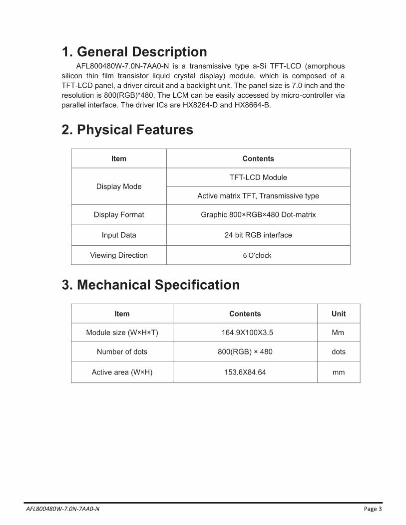
1. General Description AFL800480W-7.0N-7AA0-N is a transmissive type a-Si TFT-LCD (amorphous
silicon thin film transistor liquid crystal display) module, which is composed of a TFT-LCD panel, a driver circuit and a backlight unit. The panel size is 7.0 inch and the resolution is 800(RGB)*480, The LCM can be easily accessed by micro-controller via parallel interface. The driver ICs are HX8264-D and HX8664-B.
2. Physical Features
stnetnoC metI
Display Mode TFT-LCD Module
Active matrix TFT, Transmissive type
Display Format Graphic 800×RGB×480 Dot-matrix
ecafretni BGR tib 42 ataD tupnI
Viewing Direction 6 O’clock
3. Mechanical Specification
stnetnoC metI Unit
Module size (W×H×T) 164.9X100X3.5 Mm
Number of dots 800(RGB) × 480 dots
Active area (W×H) 153.6X84.64 mm
AFL800480W-7.0N-7AA0-N Page 4
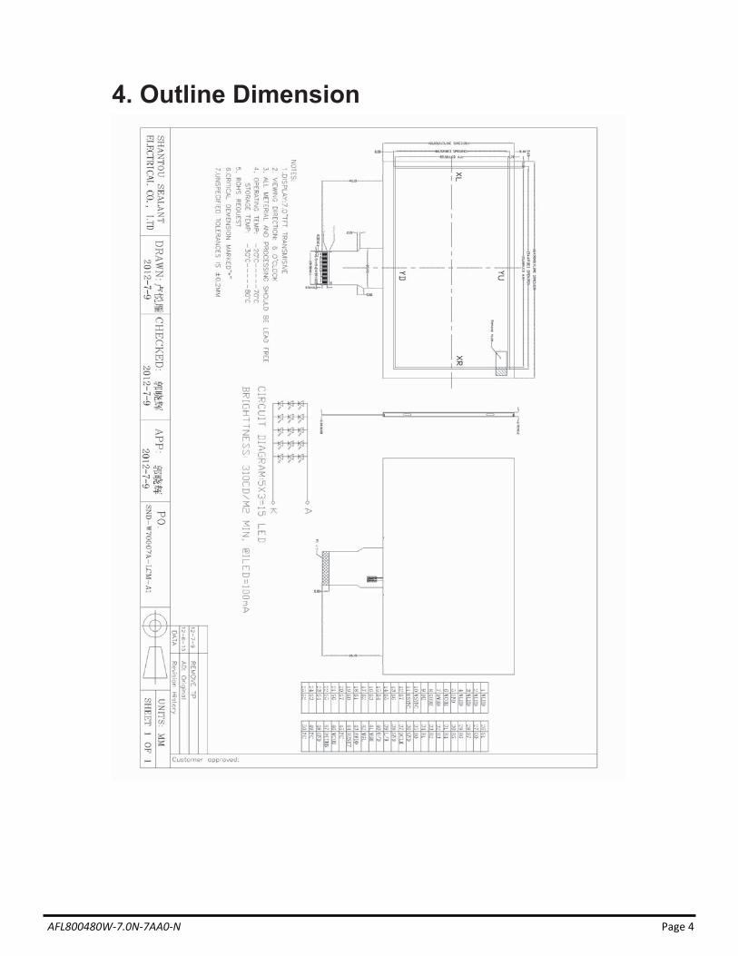
4. Outline Dimension
AFL800480W-7.0N-7AA0-N Page 5
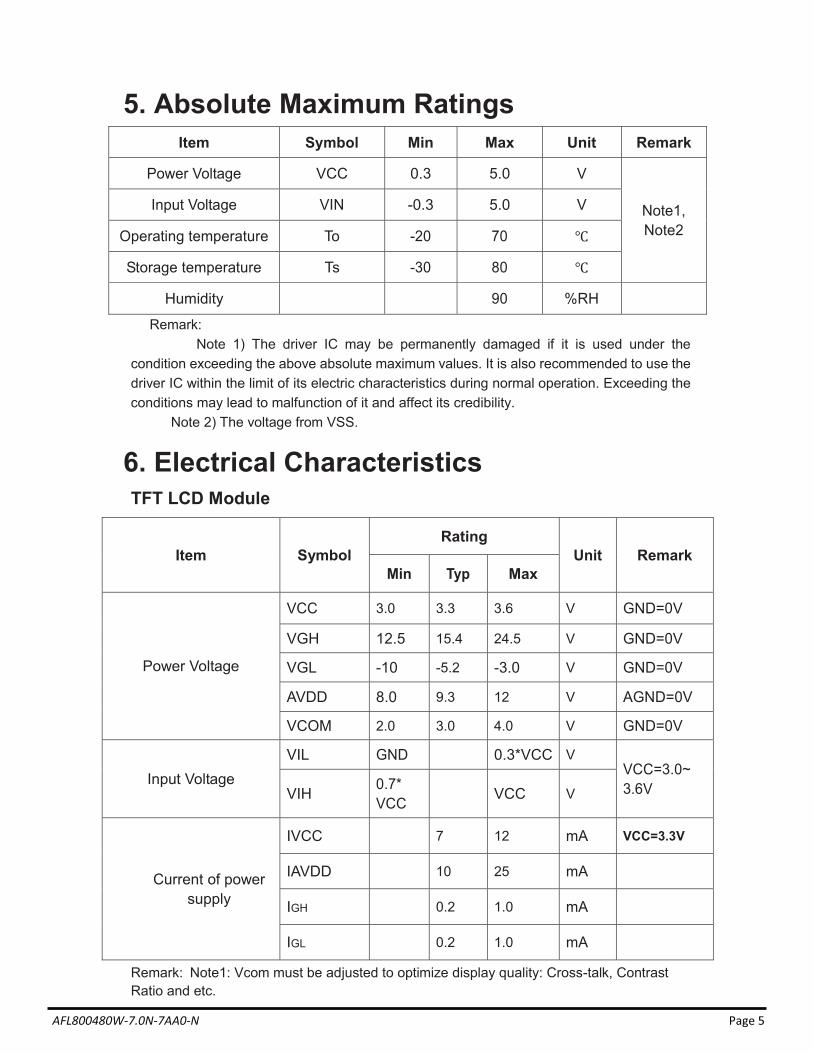
5. Absolute Maximum Ratings
Item Symbol Min Max Unit Remark
Power Voltage VCC 0.3 5.0 V
Note1, Note2
Input Voltage VIN -0.3 5.0 V
Operating temperature To -20 70
Storage temperature Ts -30 80
Humidity 90 %RH
Remark: Note 1) The driver IC may be permanently damaged if it is used under the
condition exceeding the above absolute maximum values. It is also recommended to use the driver IC within the limit of its electric characteristics during normal operation. Exceeding the conditions may lead to malfunction of it and affect its credibility.
Note 2) The voltage from VSS.
6. Electrical Characteristics TFT LCD Module
Item Symbol Rating
Unit Remark Min Typ Max
Power Voltage
VCC 3.0 3.3 3.6 V GND=0V
VGH 12.5 15.4 24.5 V GND=0V
VGL -10 -5.2 -3.0 V GND=0V
AVDD 8.0 9.3 12 V AGND=0V
VCOM 2.0 3.0 4.0 V GND=0V
Input Voltage
VIL GND 0.3*VCC V VCC=3.0~ 3.6V VIH 0.7*
VCC VCC V
Current of power supply
IVCC 7 12 mA VCC=3.3V
IAVDD 10 25 mA
IGH 0.2 1.0 mA
IGL 0.2 1.0 mA
Remark: Note1: Vcom must be adjusted to optimize display quality: Cross-talk, Contrast Ratio and etc.
AFL800480W-7.0N-7AA0-N Page 6
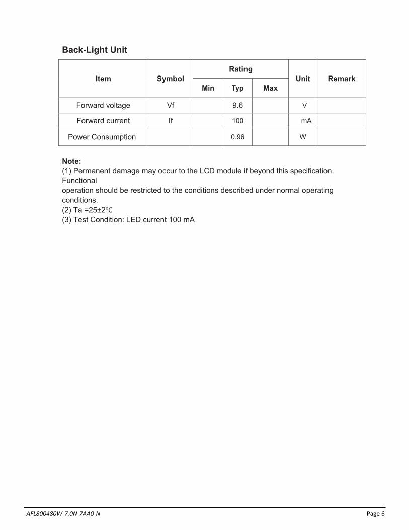
Back-Light Unit
Item Symbol Rating
Unit Remark Min Typ Max
Forward voltage Vf 9.6 V
Forward current If 100 mA
Power Consumption 0.96 W
Note: (1) Permanent damage may occur to the LCD module if beyond this specification. Functional operation should be restricted to the conditions described under normal operating conditions. (2) Ta =25±2 (3) Test Condition: LED current 100 mA
AFL800480W-7.0N-7AA0-N Page 7
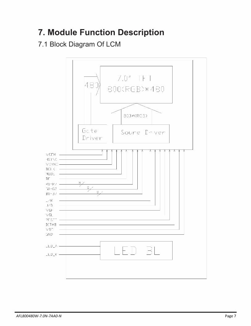
7. Module Function Description
7.1 Block Diagram Of LCM
AFL800480W-7.0N-7AA0-N Page 8
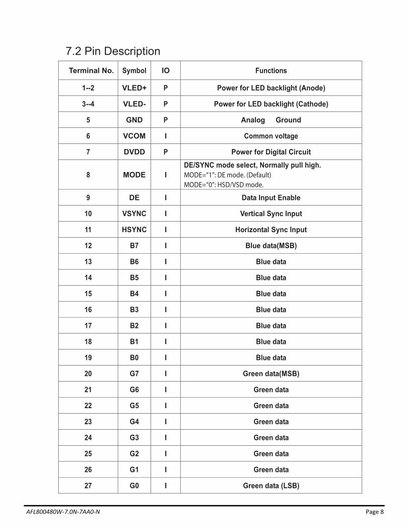
7.2 Pin Description
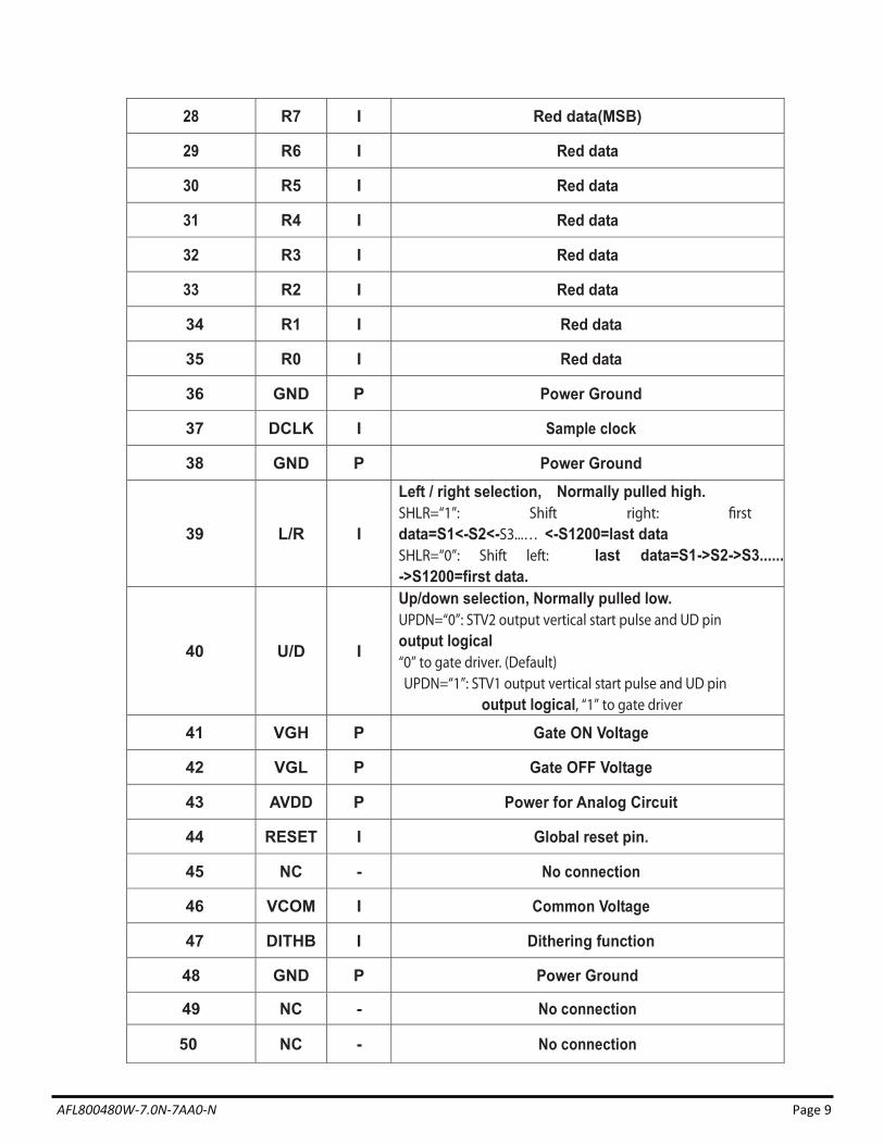
Terminal No. Symbol IO Functions
1--2 VLED+ P Power for LED backlight (Anode)
3--4 VLED- P Power for LED backlight (Cathode)
5 GND P Analog Ground
6 VCOM I Common voltage
7 DVDD P Power for Digital Circuit
8 MODE I DE/SYNC mode select, Normally pull high. MODE=“1”: DE mode. (Default) MODE=“0”: HSD/VSD mode.
9 DE I Data Input Enable
10 VSYNC I Vertical Sync Input
11 HSYNC I Horizontal Sync Input
12 B7 I Blue data(MSB)
13 B6 I Blue data
14 B5 I Blue data
15 B4 I Blue data
16 B3 I Blue data
17 B2 I Blue data
18 B1 I Blue data
19 B0 I Blue data
20 G7 I Green data(MSB)
21 G6 I Green data
22 G5 I Green data
23 G4 I Green data
24 G3 I Green data
25 G2 I Green data
26 G1 I Green data
27 G0 I Green data (LSB)
AFL800480W-7.0N-7AA0-N Page 9
28 R7 I Red data(MSB)
29 R6 I Red data
30 R5 I Red data
31 R4 I Red data
32 R3 I Red data
33 R2 I Red data
34 R1 I Red data
35 R0 I Red data
36 GND P Power Ground
37 DCLK I Sample clock
38 GND P Power Ground
39 L/R I
Left / right selection, Normally pulled high. SHLR=“1”: Shift right: firstdata=S1<-S2<-S3...… <-S1200=last data SHLR=“0”: Shift left: last data=S1->S2->S3......->S1200=first data.
40 U/D I
Up/down selection, Normally pulled low. UPDN=“0”: STV2 output vertical start pulse and UD pin output logical “0” to gate driver. (Default) UPDN=“1”: STV1 output vertical start pulse and UD pin
output logical, “1” to gate driver
41 VGH P Gate ON Voltage
42 VGL P Gate OFF Voltage
43 AVDD P Power for Analog Circuit
44 RESET I Global reset pin.
45 NC - No connection
46 VCOM I Common Voltage
47 DITHB I Dithering function
48 GND P Power Ground
49 NC - No connection
50 NC - No connection
AFL800480W-7.0N-7AA0-N Page 10
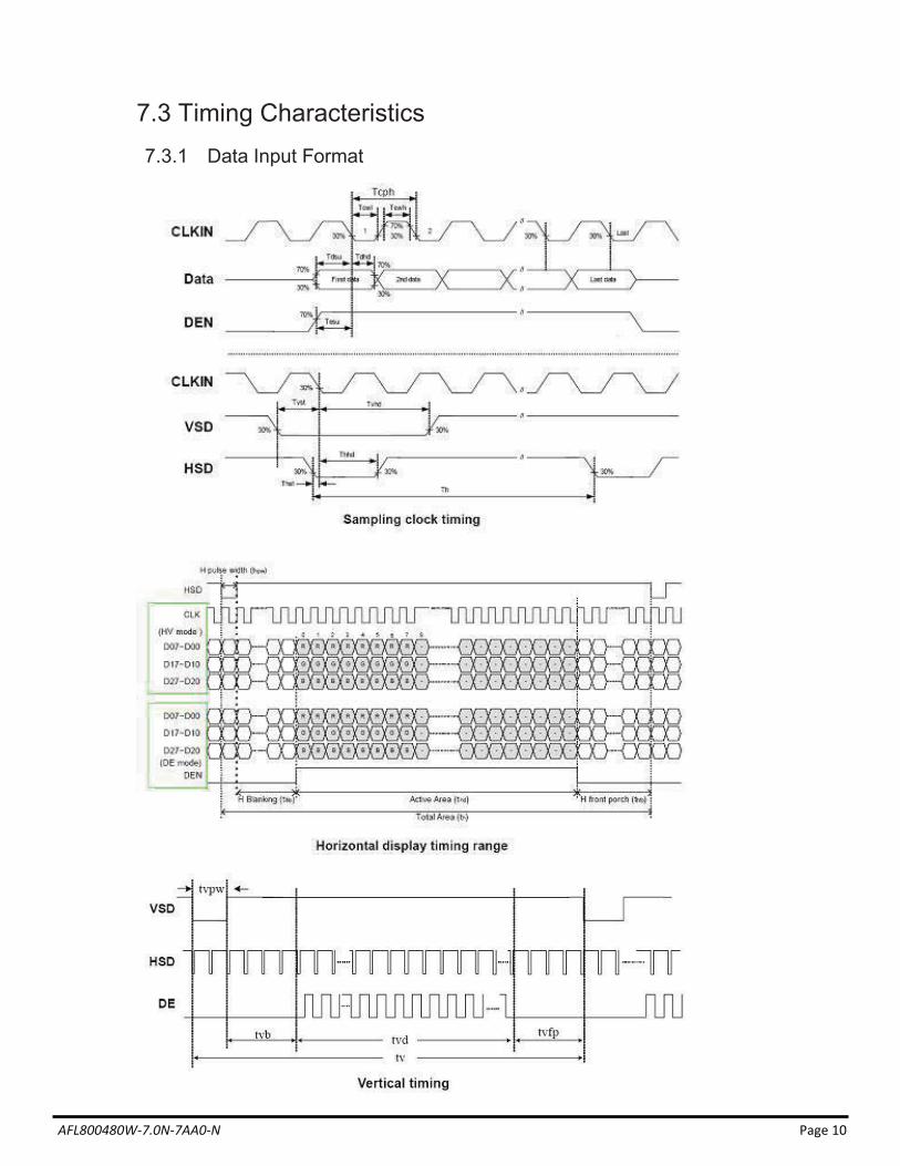
7.3 Timing Characteristics
7.3.1 Data Input Format
AFL800480W-7.0N-7AA0-N Page 11
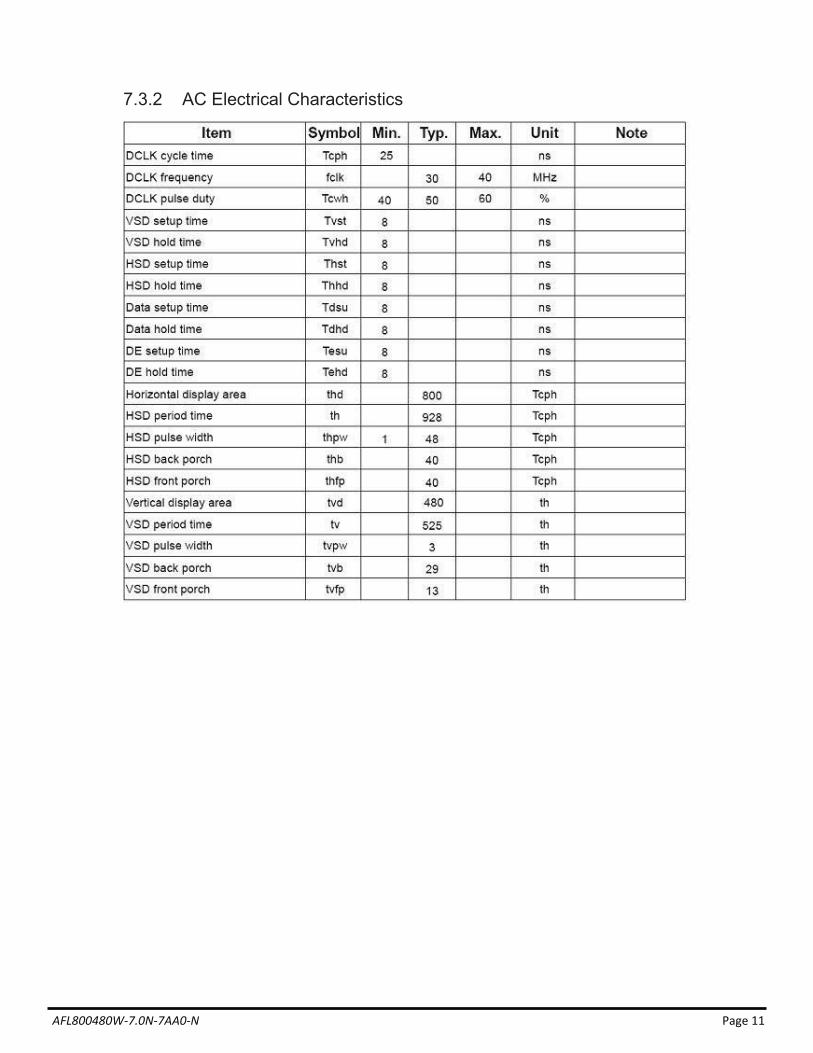
7.3.2 AC Electrical Characteristics
AFL800480W-7.0N-7AA0-N Page 12
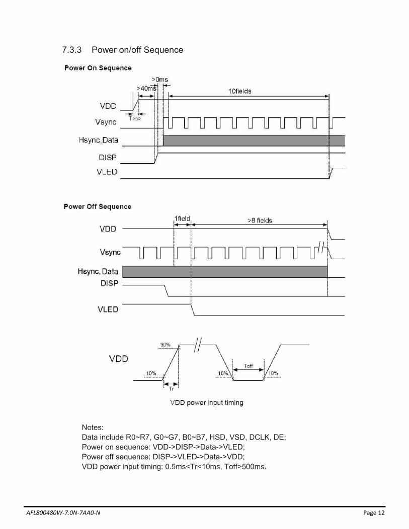
7.3.3 Power on/off Sequence
Notes: Data include R0~R7, G0~G7, B0~B7, HSD, VSD, DCLK, DE; Power on sequence: VDD->DISP->Data->VLED; Power off sequence: DISP->VLED->Data->VDD; VDD power input timing: 0.5ms<Tr<10ms, Toff>500ms.
AFL800480W-7.0N-7AA0-N Page 13
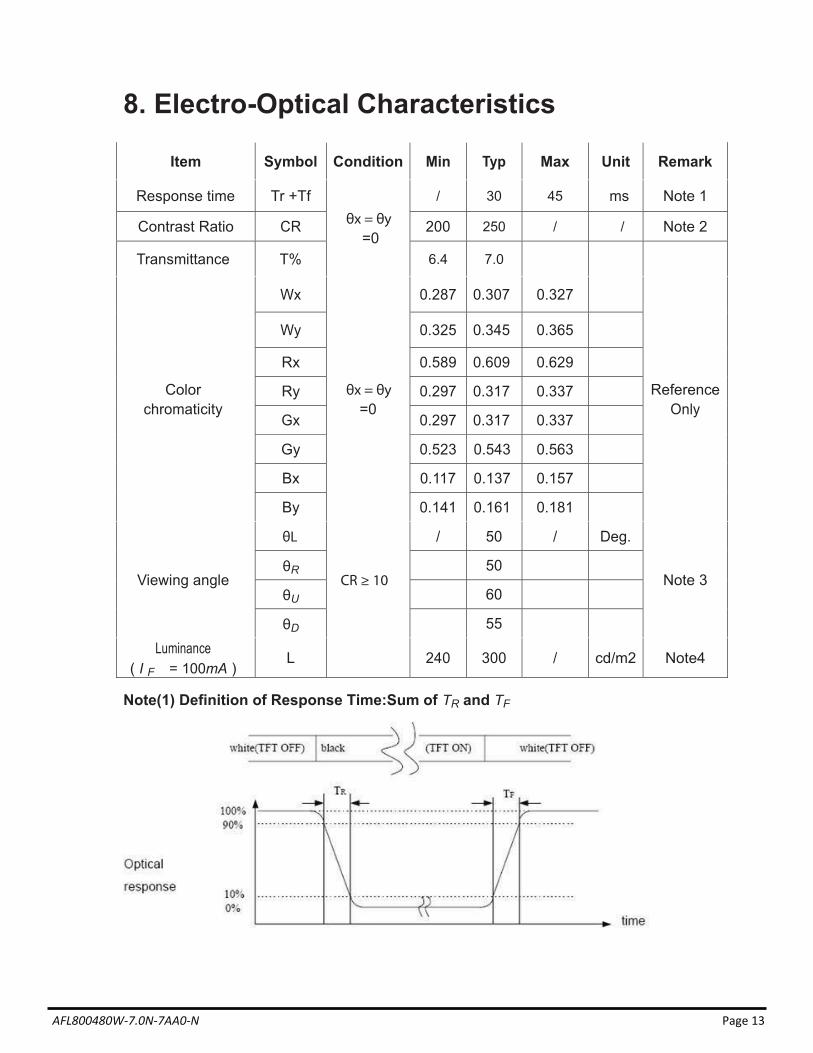
8. Electro-Optical Characteristics
Item Symbol Condition Min Typ Max Unit Remark
Response time Tr +Tf θx = θy
=0
/ 30 45 ms Note 1
Contrast Ratio CR 200 250 / / Note 2
Transmittance T% 6.4 7.0
Color chromaticity
Wx
θx = θy =0
0.287 0.307 0.327
Reference Only
Wy 0.325 0.345 0.365
Rx 0.589 0.609 0.629
Ry 0.297 0.317 0.337
Gx 0.297 0.317 0.337
Gy 0.523 0.543 0.563
Bx 0.117 0.137 0.157
By 0.141 0.161 0.181
Viewing angle
θL
CR ≥ 10
/ 50 / Deg.
Note 3 θR 50
θU 60
θD 55 Luminance
( I F = 100mA ) L 240 300 / cd/m2 Note4
Note(1) Definition of Response Time:Sum of TR and TF
AFL800480W-7.0N-7AA0-N Page 14
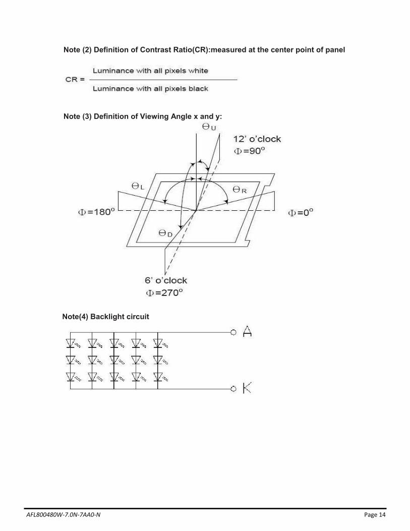
Note (2) Definition of Contrast Ratio(CR):measured at the center point of panel
Note (3) Definition of Viewing Angle x and y:
Note(4) Backlight circuit
AFL800480W-7.0N-7AA0-N Page 15
9. Reliability NO. Item Condition Criterion
1 High Temperature Storage 80 ºC, 96Hrs
No abnormalities in function and appearance
2 High Temperature Operatign 70 ºC, 96Hrs 3 Low Temperature Storage -30 ºC, 96Hrs 4 Low Temperature Operating -20 ºC, 96Hrs
5 High Temperature/Humidity Non-Operating Test 40 ºC,90%RH, 96Hrs
6 Thermal Shoc Test -20 ºC(60Min)�25 ºC(5Min)�60 ºC(60Min) 10 Cycles
10. Inspection Standards
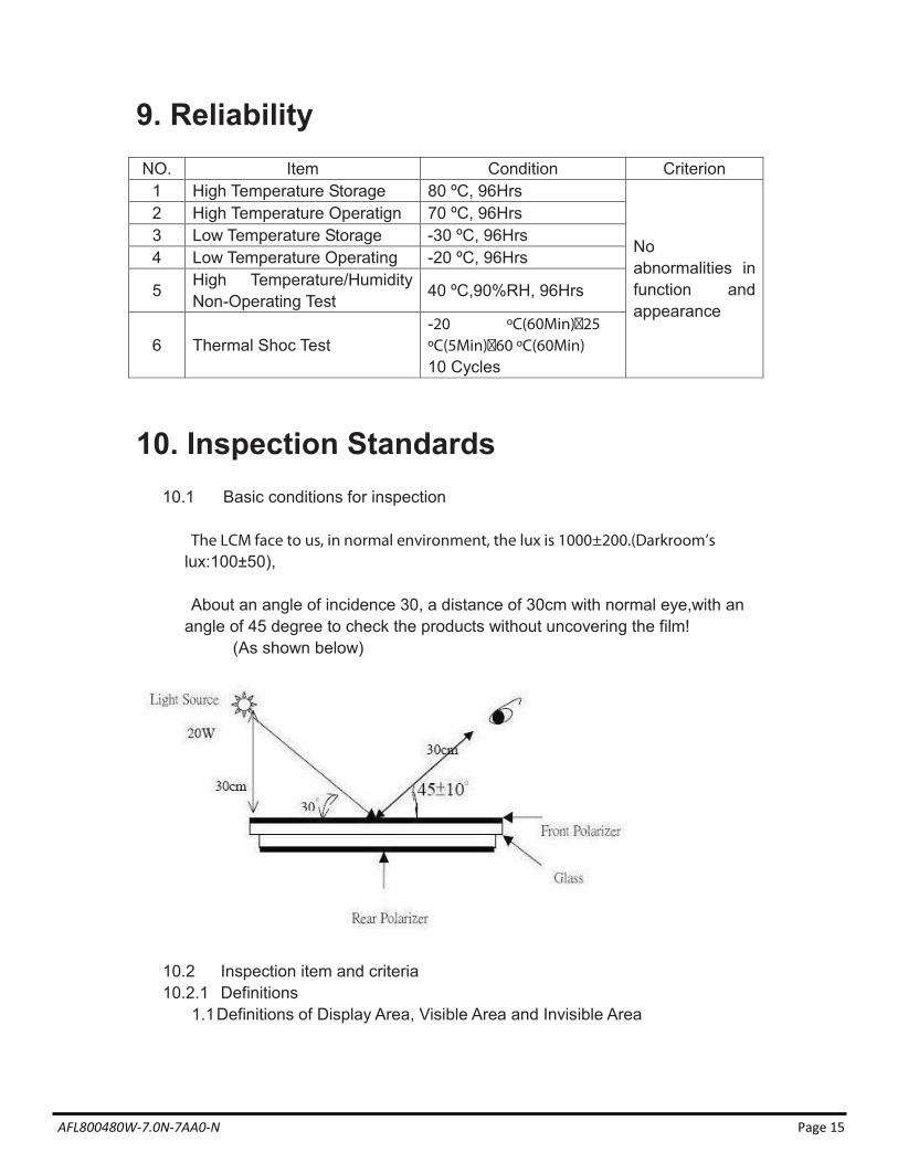
10.1 Basic conditions for inspection
The LCM face to us, in normal environment, the lux is 1000±200.(Darkroom’s lux:100±50),
About an angle of incidence 30, a distance of 30cm with normal eye,with an
angle of 45 degree to check the products without uncovering the film! (As shown below)
10.2 Inspection item and criteria 10.2.1 Definitions
1.1 Definitions of Display Area, Visible Area and Invisible Area
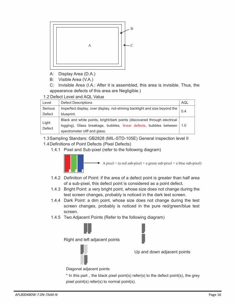
AFL800480W-7.0N-7AA0-N Page 16
A: Display Area (D.A.) B: Visible Area (V.A.) C: Invisible Area (I.A.: After it is assembled, this area is invisible. Thus, the appearance defects of this area are Negligible.)
1.2 Defect Level and AQL Value Level Defect Descriptions AQL Serious Defect
Imperfect display, over display, not-shining backlight and size beyond the blueprint.
0.4
Light Defect
Black and white points, bright/dark points (discovered through electrical logging), Glass breakage, bubbles, linear defects, bubbles between spectrometer cliff and glass.
1.0
1.3 Sampling Standars: GB2828 (MIL-STD-105E) General inspection level II 1.4 Definitions of Point Defects (Pixel Defects)
1.4.1 Pixel and Sub-pixel (refer to the following diagram)
1.4.2 Definition of Point: if the area of a defect point is greater than half area
of a sub-pixel, this defect point is considered as a point defect. 1.4.3 Bright Point: a very bright point, whose size does not change during the
test screen changes, probably is noticed in the dark test screen. 1.4.4 Dark Point: a dim point, whose size does not change during the test
screen changes, probably is noticed in the pure red/green/blue test screen.
1.4.5 Two Adjacent Points (Refer to the following diagram)
Diagonal adjacent points * In this part the black pixel point(s) refer(s) to the defect point(s), the grey pixel point(s) refer(s) to normal point(s).
Right and left adjacent points
Up and down adjacent points
C
B
A
A pixel = (a red sub-pixel + a green sub-pixel + a blue sub-pixel)
AFL800480W-7.0N-7AA0-N Page 17
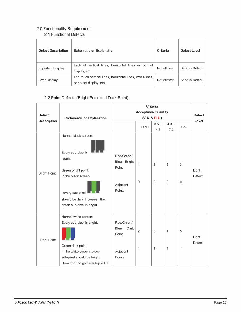
2.0 Functionality Requirement 2.1 Functional Defects
2.2 Point Defects (Bright Point and Dark Point)
Defect Description Schematic or Explanation Criteria Defect Level
Imperfect Display Lack of vertical lines, horizontal lines or do not
display, etc. Not allowed Serious Defect
Over Display Too much vertical lines, horizontal lines, cross-lines,
or do not display, etc. Not allowed Serious Defect
Defect Description
Schematic or Explanation
Criteria Acceptable Quantity
(V.A. & D.A.) Defect Level
3.5� 3.5
4.3
4.3
7.0 ≥7.0
Bright Point
Normal black screen:
Every sub-pixel is
dark.
Green bright point:
In the black screen,
every sub-pixel
should be dark. However, the
green sub-pixel is bright.
Red/Green/
Blue Bright
Point
Adjacent
Points
1
0
2
0
2
0
3
0
Light
Defect
Dark Point
Normal white screen:
Every sub-pixel is bright.
Green dark point:
In the white screen, every
sub-pixel should be bright.
However, the green sub-pixel is
Red/Green/
Blue Dark
Point
Adjacent
Points
2
1
3
1
4
1
5
1
Light
Defect
AFL800480W-7.0N-7AA0-N Page 18
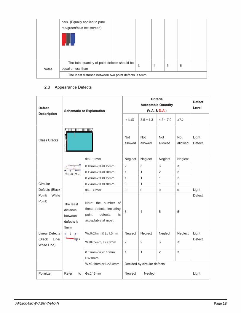
2.3 Appearance Defects
dark. (Equally applied to pure
red/green/blue test screen)
Notes
The total quantity of point defects should be
equal or less than 3 4 5 5
The least distance between two point defects is 5mm.
Defect Description
Schematic or Explanation
Criteria Acceptable Quantity
(V.A. & D.A.)
Defect Level
3.5� 3.5 4.3 4.3 7.0 ≥7.0
Glass Cracks
Not
allowed
Not
allowed
Not
allowed
Not
allowed
Light
Defect
Circular
Defects (Black
Point/ White
Point)
The least
distance
between
defects is
5mm.
Φ≤0.10mm Neglect Neglect Neglect Neglect
Light
Defect
0.10mm<Φ≤0.15mm 2 3 3 3
0.15mm<Φ≤0.20mm 1 1 2 2
0.20mm<Φ≤0.25mm 1 1 1 2
0.25mm<Φ≤0.30mm 0 1 1 1
Φ>0.30mm 0 0 0 0
Note: the number of
these defects, including
point defects, is
acceptable at most.
3 4 5 5
Linear Defects
(Black Line/
White Line)
W≤0.03mm & L≤1.0mm Neglect Neglect Neglect Neglect Light
Defect W≤0.05mm, L≤2.0mm 2 2 3 3
0.05mm<W≤0.10mm,
L≤2.0mm
1 1 2 3
W>0.1mm or L>2.0mm Decided by circular defects
Polarizer Refer to Φ≤0.15mm Neglect Neglect Light
AFL800480W-7.0N-7AA0-N Page 19
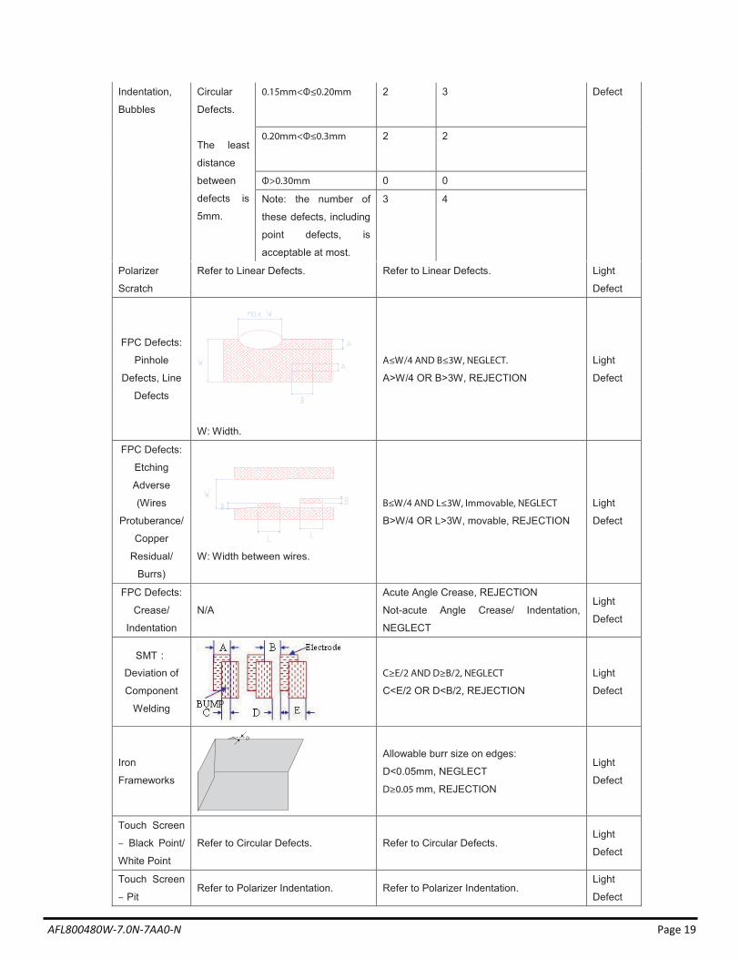
Indentation,
Bubbles
Circular
Defects.
The least
distance
between
defects is
5mm.
0.15mm<Φ≤0.20mm 2 3 Defect
0.20mm<Φ≤0.3mm 2 2
Φ>0.30mm 0 0
Note: the number of
these defects, including
point defects, is
acceptable at most.
3 4
Polarizer
Scratch
Refer to Linear Defects. Refer to Linear Defects. Light
Defect
FPC Defects:
Pinhole
Defects, Line
Defects
W: Width.
A≤W/4 AND B≤3W, NEGLECT.
A>W/4 OR B>3W, REJECTION
Light
Defect
FPC Defects:
Etching
Adverse
(Wires
Protuberance/
Copper
Residual/
Burrs)
W: Width between wires.
B≤W/4 AND L≤3W, Immovable, NEGLECT
B>W/4 OR L>3W, movable, REJECTION
Light
Defect
FPC Defects:
Crease/
Indentation
N/A
Acute Angle Crease, REJECTION
Not-acute Angle Crease/ Indentation,
NEGLECT
Light
Defect
SMT
Deviation of
Component
Welding
C≥E/2 AND D≥B/2, NEGLECT
C<E/2 OR D<B/2, REJECTION
Light
Defect
Iron
Frameworks
D
Allowable burr size on edges:
D<0.05mm, NEGLECT
D≥0.05 mm, REJECTION
Light
Defect
Touch Screen
– Black Point/
White Point
Refer to Circular Defects. Refer to Circular Defects. Light
Defect
Touch Screen
– Pit Refer to Polarizer Indentation. Refer to Polarizer Indentation.
Light
Defect
AFL800480W-7.0N-7AA0-N Page 20
11. Precautions For Using LCD Modules 11.1 Mounting method The LCD panel of Daxian LCD module consists of two thin glass plates with polarizes
which easily be damaged. And since the module in so constructed as to be fixed by utilizing fitting holes in the printed circuit board.
Extreme care should be needed when handling the LCD modules. 11.2 Caution of LCD handling and cleaning When cleaning the display surface, Use soft cloth with solvent [recommended below]
and wipe lightly Isopropyl alcohol Ethyl alcohol
Do not wipe the display surface with dry or hard materials that will damage the polarizer surface.
Do not use the following solvent: Water Aromatics
Do not wipe ITO pad area with the dry or hard materials that will damage the ITO patterns
Do not use the following solvent on the pad or prevent it from eingcontaminated: Soldering flux Chlorine (Cl) , Salfur (S)
If goods were sent without being sili8con coated on the pad, ITO patterns could be damaged due to the corrosion as time goes on.
If ITO corrosion happen by miss-handling or using some materials such as Chlorine (CI), Salfur (S) from customer, Responsibility is on customer.
11.3 Caution against static charge The LCD module use C-MOS LSI drivers, so we recommended that you: Connect any
unused input terminal to Vdd or Vss, do not input any signals before power is turned on, and ground your body, work/assembly areas, assembly equipment to protect against static electricity.
Touch Screen
– Scratch
Refer to Linear Defects. Refer to Linear Defects. Light
Defect
Touch Screen
– Newton’s
Ring
Regular Newton’s Ring:
Irregular Newton’s Ring:
Area of Newton’s Ring ≤ 1/3 Total Display
Ares, NEGLECT.
Area of Newton’s Ring > 1/3 Total Display
Ares, REJECTION.
Area of Newton’s Ring ≤ 1/2 Total Display
Ares, NEGLECT
Area of Newton’s Ring > 1/2 Total Display
Ares, REJECTION
Note: if Newton’s Ring ca uses graphic
distortion, please REJECT.
Light
Defect
AFL800480W-7.0N-7AA0-N Page 21
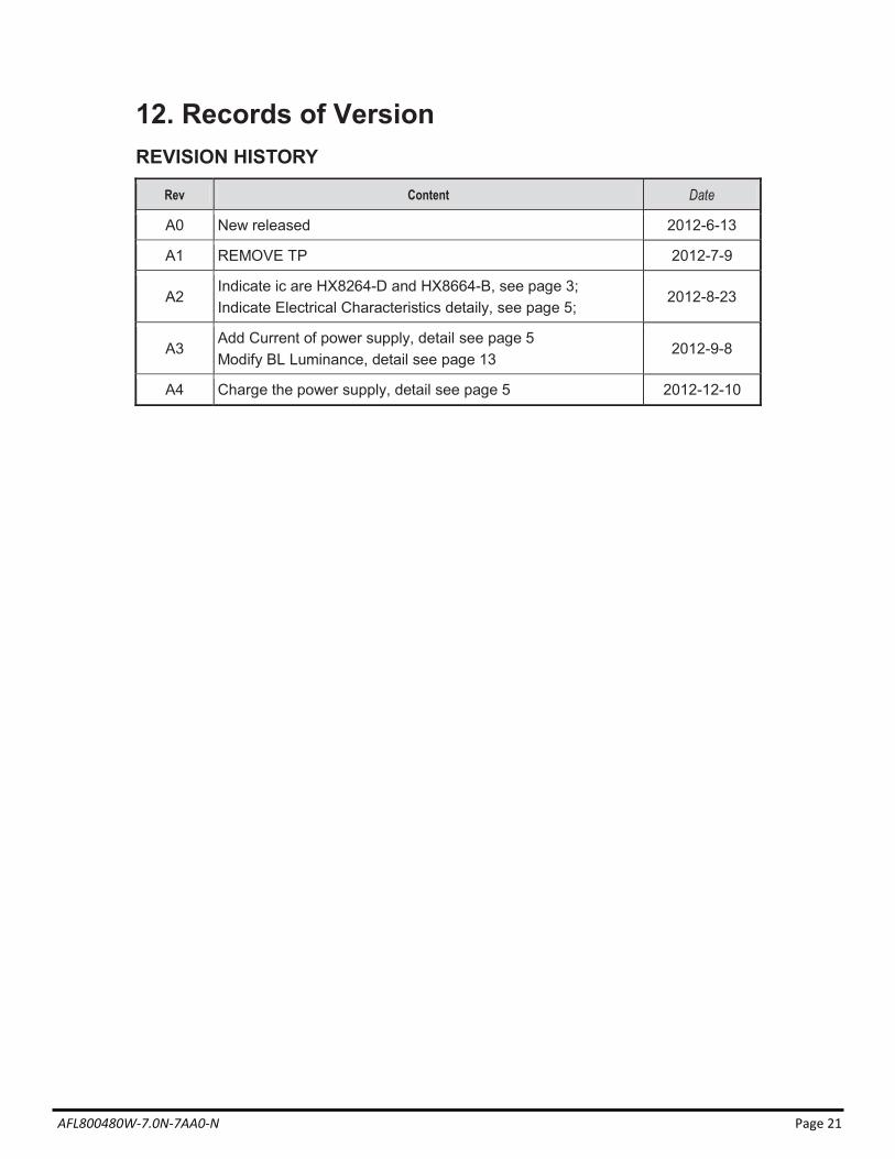
12. Records of Version REVISION HISTORY
Rev Content Date
A0 New released 2012-6-13
A1 REMOVE TP 2012-7-9
A2 Indicate ic are HX8264-D and HX8664-B, see page 3; Indicate Electrical Characteristics detaily, see page 5;
2012-8-23
A3 Add Current of power supply, detail see page 5 Modify BL Luminance, detail see page 13
2012-9-8
A4 Charge the power supply, detail see page 5 2012-12-10