Embed Size (px)
Citation preview
Specification Developers Kit A9M2410
ModARM9 with Samsung S3C2410A/S3C2440A
22. December 2004
P.O. Box 1103 D-79200 Breisach, GermanyKueferstrasse 8 D-79206 Breisach, Germany
+49 (7667) 908-0 Fax +49 (7667) 908-200 [email protected] http://www.fsforth.de
Specification Developers Kit A9M2410, ModARM9 with SamsungS3C2410A/S3C2440A
Joachim Jaeger, 22. December 2004 - Page 2/32 - m:\modarm9\spec_devkit_a9m2410c.doc
Table of Contents:1. History .................................................................................................................................. 42. Overview .............................................................................................................................. 53. Market Requirements ........................................................................................................... 54. Features of the Base Board ................................................................................................. 65. Components of the Developer’s Kit ...................................................................................... 76. Detailed Specification........................................................................................................... 7
6.1. Module Signals ..............................................................................................................76.2. Power Supply ................................................................................................................76.3. Debug LED ....................................................................................................................86.4. RESET Control ..............................................................................................................86.5. JTAG Interfaces.............................................................................................................86.6. Configuration Switches..................................................................................................86.7. Configuration Jumpers ..................................................................................................96.8. RS232 Interface.............................................................................................................96.9. USB Interfaces ..............................................................................................................96.10.Ethernet Interface..........................................................................................................96.11.CompactFlash Interface ................................................................................................96.12.LCD Interface ..............................................................................................................106.13.Touch Screen..............................................................................................................106.14.Audio Codec................................................................................................................106.15.SD Interface ................................................................................................................106.16.Camera Interface ........................................................................................................106.17.CAN interface..............................................................................................................106.18.Extension Connectors .................................................................................................106.19.Expansion Connectors ................................................................................................11
7. Mechanics .......................................................................................................................... 127.1. Standard Module .........................................................................................................127.2. Extended Module.........................................................................................................12
8. General Connectors ........................................................................................................... 138.1. Connector JTAG Booster CPU, X7 .............................................................................138.2. Connector JTAG Booster CPLD, X25 .........................................................................138.3. Connector JTAG Multi-ICE, X6....................................................................................138.4. Connector COMA, X12................................................................................................148.5. Connector COMB, X13................................................................................................148.6. Connector COMC, X8..................................................................................................148.7. Ethernet Connector 10/100Mbit/s, X16 .......................................................................158.8. Connector USB Host, X14...........................................................................................158.9. Connector USB Device, X15 .......................................................................................158.10.Connector CAN, X9.....................................................................................................158.11.Connector Camera, X28 .............................................................................................168.12.Connector LCD, X26...................................................................................................168.13.Connector Touch Screen, X27....................................................................................178.14.Compact Flash Socket, X18........................................................................................178.15.Connector SD Card, X29 ............................................................................................188.16.External 5V Power, X5 ................................................................................................18
9. Board to Board Connectors................................................................................................ 199.1. System Connector X1..................................................................................................199.2. System Connector X2..................................................................................................239.3. System Connector X3..................................................................................................269.4. System Connector X4..................................................................................................27
10. Appendix A: Expansion Connectors ................................................................................... 2910.1.Module Connector X1 versus Expansion Connectors X10/X11..................................2910.2.Module Connector X2 versus Expansion Connectors X20/X21..................................30
Specification Developers Kit A9M2410, ModARM9 with SamsungS3C2410A/S3C2440A
Joachim Jaeger, 22. December 2004 - Page 3/32 - m:\modarm9\spec_devkit_a9m2410c.doc
10.3.Module Connector X3 versus Expansion Connectors X30, X31.................................3110.4.Module Connector X4 versus Expansion Connectors X40, X41.................................32
Specification Developers Kit A9M2410, ModARM9 with SamsungS3C2410A/S3C2440A
Joachim Jaeger, 22. December 2004 - Page 4/32 - m:\modarm9\spec_devkit_a9m2410c.doc
1. History
Date Version Responsible Description18.08.2004 0.1 J. Jaeger Initial Version07.10.2004 0.2 J. Jaeger Chapter SD card interface modified12.11.2004 0.3 J. Jaeger Connectors updated16.11.2004 1.0 J. Jaeger Application specific items added to system
connectors22.12.2004 1.1 J. Jaeger Chapter Touch screen updated

Specification Developers Kit A9M2410, ModARM9 with SamsungS3C2410A/S3C2440A
Joachim Jaeger, 22. December 2004 - Page 5/32 - m:\modarm9\spec_devkit_a9m2410c.doc
2. Overview
The A9M2410 Developer’s Kit consists of the module together with a base board, cabling,documentation and software. Two A9M2410 Developer’s Kits are available: one for Linux(LxNETES v3.0) and one for Windows CE .NET 4.2.
3. Market Requirements
The various ARM-based SoCs that are now available typically address specific marketsegments. It is now relatively easy for companies who are silicon market leaders in a nichesegment to add an ARM core to their silicon and so provide a single chip solution reducing costand complexity to their end customers. A typical example of this is the Micrel KS8695 which hasbeen designed as a residential gateway for SOHO applications.
Although the ARM-based SoCs have been designed for a particular market, it does not meanthat a module with this SoC on it should address the same market. So the markets we want toaddress with ModARM9 modules are still the ones where we have been successful in the past.The Samsung module will target applications requiring a GUI but not an Ethernet connection(the optional 10Mbps Ethernet interface is intended for debugging purposes only) and be able todo this competitively. This means that the following markets can be addressed:
• Industrial automation
• Retail point-of-sale
• Medical equipment
• Mobile applications (battery-powered)
The emphasis on the GUI will probably mean that Windows CE .NET will be more popular onthe A9M2410 than Linux, which has it strength in networking applications.
Specification Developers Kit A9M2410, ModARM9 with SamsungS3C2410A/S3C2440A
Joachim Jaeger, 22. December 2004 - Page 6/32 - m:\modarm9\spec_devkit_a9m2410c.doc
4. Features of the Base Board
The base board will contain the following components and interfaces:
• 5.7” TFT display (SHARP) with Touch screen
• RJ45 connector and transformer for 10/100MBit/s, with integrated LEDs
• 2 serial interfaces using DB-9P connectors
• USB connectors for host and device
• CompactFlash type-II slot
• SD Interface with normal type connector
• Audio codec (UDA1341TS) with speaker jack and connector for microphone
• CAN driver with 10pin header
• Connector for 5V power supply
• Connector (2-pin) for external Li-Ion battery will be realized on a 2nd base board, which isspecialized for Li-Ion battery, and has an own Li-Ion charger on board
• JTAG 20-pin connector and 8-pin JTAG Booster connector
• Connectors for the module signals (like on the A9Mvali), but realized as PC/104 press fitcontacts with pin on top and acceptable on the bottom.
• Connector for TFT LCD, this will be a 2row, 40pin connector.
• Reset button
• Power LED
• Debug LED
• Two user buttons
• DIP switches for configuration
• Support of A9M2440 module
Specification Developers Kit A9M2410, ModARM9 with SamsungS3C2410A/S3C2440A
Joachim Jaeger, 22. December 2004 - Page 7/32 - m:\modarm9\spec_devkit_a9m2410c.doc
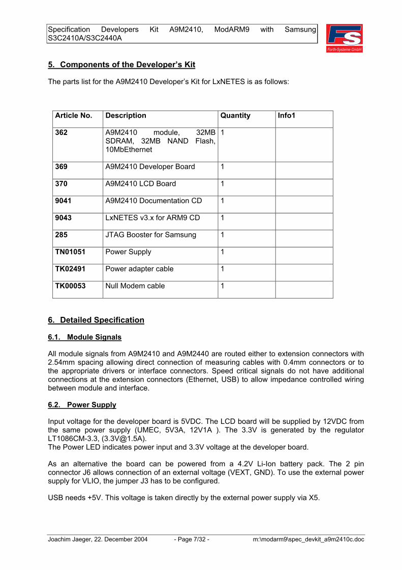
5. Components of the Developer’s Kit
The parts list for the A9M2410 Developer’s Kit for LxNETES is as follows:
Article No. Description Quantity Info1
362 A9M2410 module, 32MBSDRAM, 32MB NAND Flash,10MbEthernet
1
369 A9M2410 Developer Board 1
370 A9M2410 LCD Board 1
9041 A9M2410 Documentation CD 1
9043 LxNETES v3.x for ARM9 CD 1
285 JTAG Booster for Samsung 1
TN01051 Power Supply 1
TK02491 Power adapter cable 1
TK00053 Null Modem cable 1
6. Detailed Specification
6.1. Module Signals
All module signals from A9M2410 and A9M2440 are routed either to extension connectors with2.54mm spacing allowing direct connection of measuring cables with 0.4mm connectors or tothe appropriate drivers or interface connectors. Speed critical signals do not have additionalconnections at the extension connectors (Ethernet, USB) to allow impedance controlled wiringbetween module and interface.
6.2. Power Supply
Input voltage for the developer board is 5VDC. The LCD board will be supplied by 12VDC fromthe same power supply (UMEC, 5V3A, 12V1A ). The 3.3V is generated by the regulatorLT1086CM-3.3, ([email protected]).The Power LED indicates power input and 3.3V voltage at the developer board.
As an alternative the board can be powered from a 4.2V Li-Ion battery pack. The 2 pinconnector J6 allows connection of an external voltage (VEXT, GND). To use the external powersupply for VLIO, the jumper J3 has to be configured.
USB needs +5V. This voltage is taken directly by the external power supply via X5.
Specification Developers Kit A9M2410, ModARM9 with SamsungS3C2410A/S3C2440A
Joachim Jaeger, 22. December 2004 - Page 8/32 - m:\modarm9\spec_devkit_a9m2410c.doc
6.3. Debug LED
A green debug LED is connected with its cathode to ground. The anode has a 1K serial resistorand is wired to GPF6 to allow universal usage on the board.
6.4. RESET Control
A push button S1 allows manual RESET by connecting RSTIN# to ground. Signals RSTIN#,PWRGOOD and RSTOUT# are available on the 2.54mm extension connectors.
6.5. JTAG Interfaces
The developer board provides a 20-pin JTAG interface and an 8-pin JTAG-Booster connector,to access the CPU. A separate 8pin connector is provided to program the Lattice CPLD, whichcontains the logic to access the CompactFlash card.
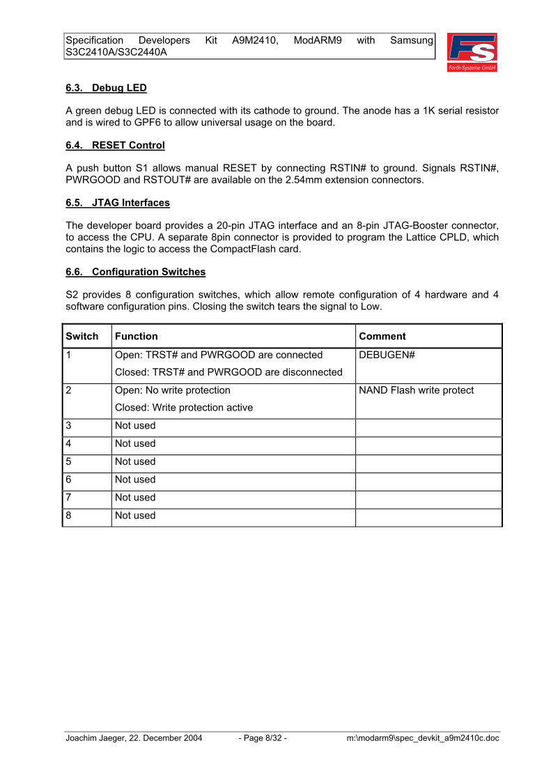
6.6. Configuration Switches
S2 provides 8 configuration switches, which allow remote configuration of 4 hardware and 4software configuration pins. Closing the switch tears the signal to Low.
Switch Function Comment
1 Open: TRST# and PWRGOOD are connected
Closed: TRST# and PWRGOOD are disconnected
DEBUGEN#
2 Open: No write protection
Closed: Write protection active
NAND Flash write protect
3 Not used
4 Not used
5 Not used
6 Not used
7 Not used
8 Not used

Specification Developers Kit A9M2410, ModARM9 with SamsungS3C2410A/S3C2440A
Joachim Jaeger, 22. December 2004 - Page 9/32 - m:\modarm9\spec_devkit_a9m2410c.doc
6.7. Configuration Jumpers
Jumper Function Comment
J1 Open: VRTC not buffered
Closed: VRTC battery buffered with G1
Battery buffering RTC
J2 Open: Transmitter U4 MAX3320 disabled
Closed: Transmitter U4 MAX3320 enabled
RS232 driver control COMA
J3 1-2: VLIO = +3.3V
2-3: VLIO = VEXT
Selection of VLIO
J4 1-2: Handshake line ERTS1#
2-3: Data line ETXD2
COMC selection
J5 1-2: Handshake line ECTS1#
2-3: Data line ERXD2
COMC selection
J6 1: VEXT, max. +4.2V
2: GND
Connector for VEXT,
NO JUMPER
J9 Open: Transmitter U15 MAX3320 disabled
Closed: Transmitter U15 MAX3320 enabled
RS232 driver control COMB
J10 Closed: CAN Termination active CAN termination 120R
6.8. RS232 Interface
Two RS232 Interfaces are realized with two MAX3320 drivers. The signals are routed to theDB9 connectors. RXD, TXD, RTS# and CTS# lines are routed to the module. The handshakesignals of UART1 could also be used as data signals for a 3rd UART2. Both signals areadditional connected to a 10pin connector, which is provided to connect to the 3rd RS232interface. Via jumpers J4 and J5, the 3rd UART can be selected.
6.9. USB Interfaces
USB connectors for USB host and USB device are provided. The 22R series resistor are placednear the connectors. The signal USB_DT/PW switches a 1k5 pull-up resistor to the USBP line.This is the necessary pull-up resistor for the recognition of a USB device.
MAX890 supervises the current limit of a connected USB device. The FAULT# output isconnected to the signal USBH0PEN.
6.10. Ethernet Interface
On the developer board an Ethernet connector for 100MHz mode, with integrated transformerand LEDs, is provided.
6.11. CompactFlash Interface
A 50 pin CompactFlash Card header Type 2 with ejector is provided. It is placed at the bottomside of the PCB. A logic device enables the access of the Compact Flash in 16bit mode.
Specification Developers Kit A9M2410, ModARM9 with SamsungS3C2410A/S3C2440A
Joachim Jaeger, 22. December 2004 - Page 10/32 - m:\modarm9\spec_devkit_a9m2410c.doc
Only 3.3V CompactFlash cards can be used.
The Lattice device ispMACH 4128 CPLD is used to realize the logic, which is necessary toaccess the CompactFlash cards. Following control and address lines are used:
CS4#, OE#, WE#, WAIT#, A0 – A9.
6.12. LCD Interface
The Sharp LQ57Q3DC02 TFT display is supported. It has a colour resolution of 18bpp. Only16bpp are supported. An additional pcb (LCDMODARM) is used, which includes the powerconnector, Backlight module, LCD connector and Touch interface connector. The signal linesfrom the LCD to the developer board are connected by a 40pin flat ribbon cable. 22R seriesresistors are provided at the CLK lines.
6.13. Touch Screen
The internal touch screen controller of the A9M24xx module is used. Therefore only a connector(for the A9M2410 additional 4 FETs) is necessary on the developer board. The signal lines fromthe touch screen to the developer board are connected by a 10pin flat ribbon cable.
The analog signals from the touch screen are connected to the analog inputs AIN5 and AIN7 forthe A9M2410 module and to AIN4, AIN5, AIN6, AIN7 for the A9M2440 module. The A9M2440module doesn’t need the external FETs at the developer board. Therefor pull-up or pull-downresistors are placed at the gate of each FET to disable it, in case of using an A9M2440 module.
At the board following patch is necessary to get the touch interface running for the S3C2410:
• Remove resistors R69, R70. • Remove C63 and connect it between R65 (AIN7) and AGND. • Remove C64 and connect it between R68 (AIN5) and AGND.
6.14. Audio Codec
The UDA1341TS is used as audio codec. It is connected to the IIS-interface of the S3C2410. Aspeaker, a microphone and a line-in jack is provided at the developer board.
6.15. SD Interface
A SD card holder from Molex is used to realize the SD interface. The card holder is normal type,which means it is mounted at the top side.
6.16. Camera Interface
The camera specific signals (A9M2440 only), are routed together to a 20pin dual row connector.These signals are not buffered and may used only in 3.3V environment.
6.17. CAN interface
A CAN driver is provided on the board with a 10pin header to connect to a 9pin SubD connectorvia flat cable. If a customer wants to use the CAN interface, the CAN4MODARM9 board has tobe plugged between the A9M2410 module and the base board. If CAN4MODARM is used,CS3# will be used to access the CAN controller.
6.18. Extension Connectors
Specification Developers Kit A9M2410, ModARM9 with SamsungS3C2410A/S3C2440A
Joachim Jaeger, 22. December 2004 - Page 11/32 - m:\modarm9\spec_devkit_a9m2410c.doc
Extension connectors are provided to support also the extended version of the A9M2410module. The signals are connected to the corresponding expansion connectors. The signalshave to be defined.
6.19. Expansion Connectors
The board provides expansion connectors, which can be used to plug onto a customized board.Most of the signals from the module are connected to these expansion connectors.
Specification Developers Kit A9M2410, ModARM9 with SamsungS3C2410A/S3C2440A
Joachim Jaeger, 22. December 2004 - Page 12/32 - m:\modarm9\spec_devkit_a9m2410c.doc
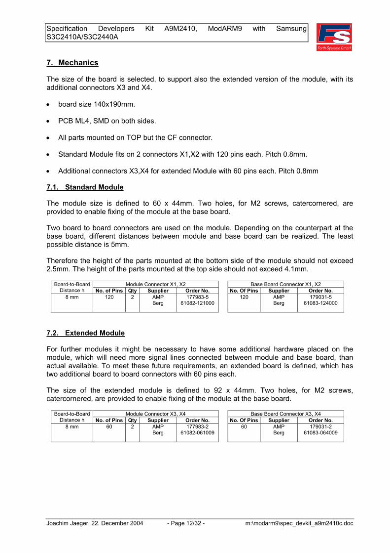
7. Mechanics
The size of the board is selected, to support also the extended version of the module, with itsadditional connectors X3 and X4.
• board size 140x190mm.
• PCB ML4, SMD on both sides.
• All parts mounted on TOP but the CF connector.
• Standard Module fits on 2 connectors X1,X2 with 120 pins each. Pitch 0.8mm.
• Additional connectors X3,X4 for extended Module with 60 pins each. Pitch 0.8mm
7.1. Standard Module
The module size is defined to 60 x 44mm. Two holes, for M2 screws, catercornered, areprovided to enable fixing of the module at the base board.
Two board to board connectors are used on the module. Depending on the counterpart at thebase board, different distances between module and base board can be realized. The leastpossible distance is 5mm.
Therefore the height of the parts mounted at the bottom side of the module should not exceed2.5mm. The height of the parts mounted at the top side should not exceed 4.1mm.
Module Connector X1, X2 Base Board Connector X1, X2Board-to-BoardDistance h No. of Pins Qty Supplier Order No. No. Of Pins Supplier Order No.
8 mm 120 2 AMPBerg
177983-561082-121000
120 AMPBerg
179031-561083-124000
7.2. Extended Module
For further modules it might be necessary to have some additional hardware placed on themodule, which will need more signal lines connected between module and base board, thanactual available. To meet these future requirements, an extended board is defined, which hastwo additional board to board connectors with 60 pins each.
The size of the extended module is defined to 92 x 44mm. Two holes, for M2 screws,catercornered, are provided to enable fixing of the module at the base board.
Module Connector X3, X4 Base Board Connector X3, X4Board-to-BoardDistance h No. of Pins Qty Supplier Order No. No. Of Pins Supplier Order No.
8 mm 60 2 AMPBerg
177983-261082-061009
60 AMPBerg
179031-261083-064009
Specification Developers Kit A9M2410, ModARM9 with SamsungS3C2410A/S3C2440A
Joachim Jaeger, 22. December 2004 - Page 13/32 - m:\modarm9\spec_devkit_a9m2410c.doc
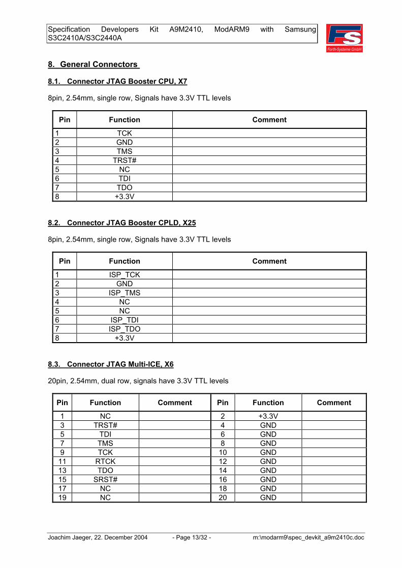
8. General Connectors
8.1. Connector JTAG Booster CPU, X7
8pin, 2.54mm, single row, Signals have 3.3V TTL levels
Pin Function Comment
1 TCK2 GND3 TMS4 TRST#5 NC6 TDI7 TDO8 +3.3V
8.2. Connector JTAG Booster CPLD, X25
8pin, 2.54mm, single row, Signals have 3.3V TTL levels
Pin Function Comment
1 ISP_TCK2 GND3 ISP_TMS4 NC5 NC6 ISP_TDI7 ISP_TDO8 +3.3V
8.3. Connector JTAG Multi-ICE, X6
20pin, 2.54mm, dual row, signals have 3.3V TTL levels
Pin Function Comment Pin Function Comment
1 NC 2 +3.3V3 TRST# 4 GND5 TDI 6 GND7 TMS 8 GND9 TCK 10 GND
11 RTCK 12 GND13 TDO 14 GND15 SRST# 16 GND17 NC 18 GND19 NC 20 GND

Specification Developers Kit A9M2410, ModARM9 with SamsungS3C2410A/S3C2440A
Joachim Jaeger, 22. December 2004 - Page 14/32 - m:\modarm9\spec_devkit_a9m2410c.doc
8.4. Connector COMA, X12
D-SUB 9 pin male, signals have RS232 levels
Pin Function Comment
1 NC2 ERXD03 ETXD04 NC5 GND6 NC7 ERTS0#8 ECTS0#9 NC
8.5. Connector COMB, X13
D-SUB 9 pin male, signals have RS232 levels
Pin Function Comment
1 NC2 ERXD13 ETXD14 NC5 GND6 NC7 ERTS1#8 ECTS1#9 NC
8.6. Connector COMC, X8
10pin, 2.54mm, dual row
Pin Function Comment Pin Function Comment
1 NC 2 NC3 ERXD2 4 NC5 ETXD2 6 NC7 NC 8 NC9 GND 10 GND

Specification Developers Kit A9M2410, ModARM9 with SamsungS3C2410A/S3C2440A
Joachim Jaeger, 22. December 2004 - Page 15/32 - m:\modarm9\spec_devkit_a9m2410c.doc
8.7. Ethernet Connector 10/100Mbit/s, X16
RJ45 8 pin, with integrated LED and magnetics
Pin Function Comment
1 TX+2 TX-3 RX+4 VGND15 VGND16 RX-7 VGND28 VGND2
8.8. Connector USB Host, X14
4pin Type A
Pin Function Comment
1 +5V2 USBN3 USBP4 GND
8.9. Connector USB Device, X15
4pin Type B
Pin Function Comment
1 NC2 USBN3 USBP4 GND
8.10. Connector CAN, X9
10pin, 2.54mm, dual row
Pin Function Comment Pin Function Comment
1 NC 2 GND3 CANL 4 CANH5 GND 6 NC7 NC 8 NC9 NC 10 NC
Specification Developers Kit A9M2410, ModARM9 with SamsungS3C2410A/S3C2440A
Joachim Jaeger, 22. December 2004 - Page 16/32 - m:\modarm9\spec_devkit_a9m2410c.doc
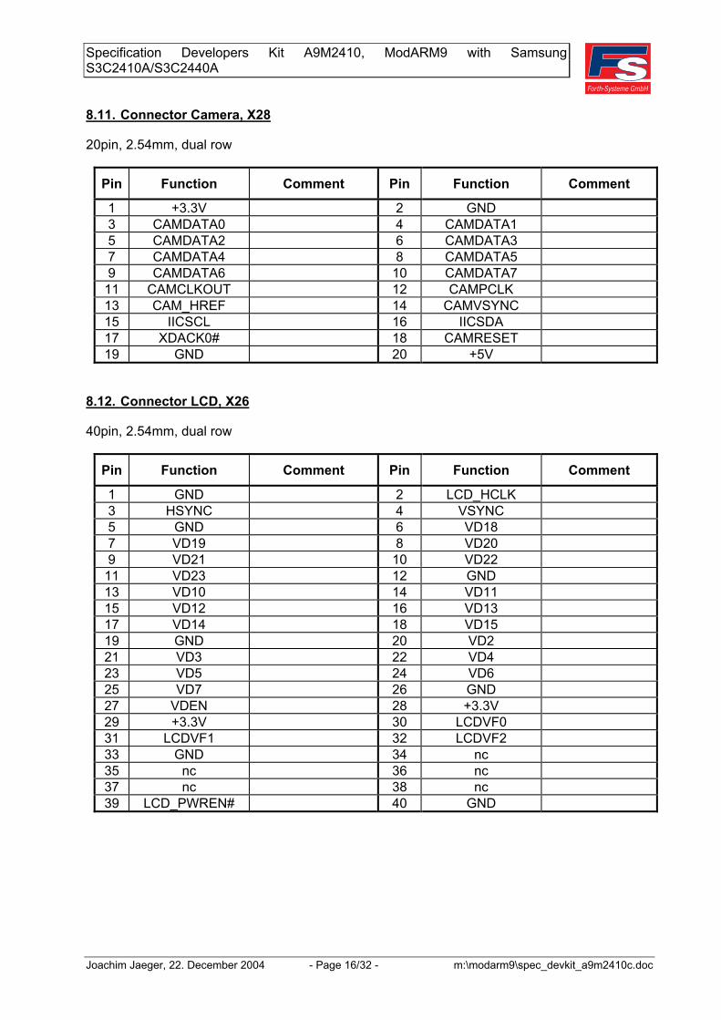
8.11. Connector Camera, X28
20pin, 2.54mm, dual row
Pin Function Comment Pin Function Comment
1 +3.3V 2 GND3 CAMDATA0 4 CAMDATA15 CAMDATA2 6 CAMDATA37 CAMDATA4 8 CAMDATA59 CAMDATA6 10 CAMDATA7
11 CAMCLKOUT 12 CAMPCLK13 CAM_HREF 14 CAMVSYNC15 IICSCL 16 IICSDA17 XDACK0# 18 CAMRESET19 GND 20 +5V
8.12. Connector LCD, X26
40pin, 2.54mm, dual row
Pin Function Comment Pin Function Comment
1 GND 2 LCD_HCLK3 HSYNC 4 VSYNC5 GND 6 VD187 VD19 8 VD209 VD21 10 VD22
11 VD23 12 GND13 VD10 14 VD1115 VD12 16 VD1317 VD14 18 VD1519 GND 20 VD221 VD3 22 VD423 VD5 24 VD625 VD7 26 GND27 VDEN 28 +3.3V29 +3.3V 30 LCDVF031 LCDVF1 32 LCDVF233 GND 34 nc35 nc 36 nc37 nc 38 nc39 LCD_PWREN# 40 GND
Specification Developers Kit A9M2410, ModARM9 with SamsungS3C2410A/S3C2440A
Joachim Jaeger, 22. December 2004 - Page 17/32 - m:\modarm9\spec_devkit_a9m2410c.doc
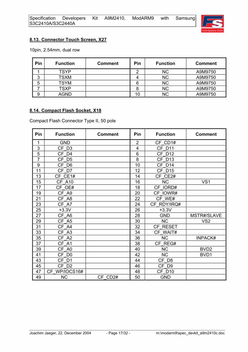
8.13. Connector Touch Screen, X27
10pin, 2.54mm, dual row
Pin Function Comment Pin Function Comment
1 TSYP 2 NC A9M97503 TSXM 4 NC A9M97505 TSYM 6 NC A9M97507 TSXP 8 NC A9M97509 AGND 10 NC A9M9750
8.14. Compact Flash Socket, X18
Compact Flash Connector Type II, 50 pole
Pin Function Comment Pin Function Comment
1 GND 2 CF_CD1#3 CF_D3 4 CF_D115 CF_D4 6 CF_D127 CF_D5 8 CF_D139 CF_D6 10 CF_D14
11 CF_D7 12 CF_D1513 CF_CE1# 14 CF_CE2#15 CF_A10 16 NC VS117 CF_OE# 18 CF_IORD#19 CF_A9 20 CF_IOWR#21 CF_A8 22 CF_WE#23 CF_A7 24 CF_RDY/IRQ#25 +3.3V 26 +3.3V27 CF_A6 28 GND MSTR#/SLAVE29 CF_A5 30 NC VS231 CF_A4 32 CF_RESET33 CF_A3 34 CF_WAIT#35 CF_A2 36 NC INPACK#37 CF_A1 38 CF_REG#39 CF_A0 40 NC BVD241 CF_D0 42 NC BVD143 CF_D1 44 CF_D845 CF_D2 46 CF_D947 CF_WP/IOCS16# 48 CF_D1049 NC CF_CD2# 50 GND
Specification Developers Kit A9M2410, ModARM9 with SamsungS3C2410A/S3C2440A
Joachim Jaeger, 22. December 2004 - Page 18/32 - m:\modarm9\spec_devkit_a9m2410c.doc
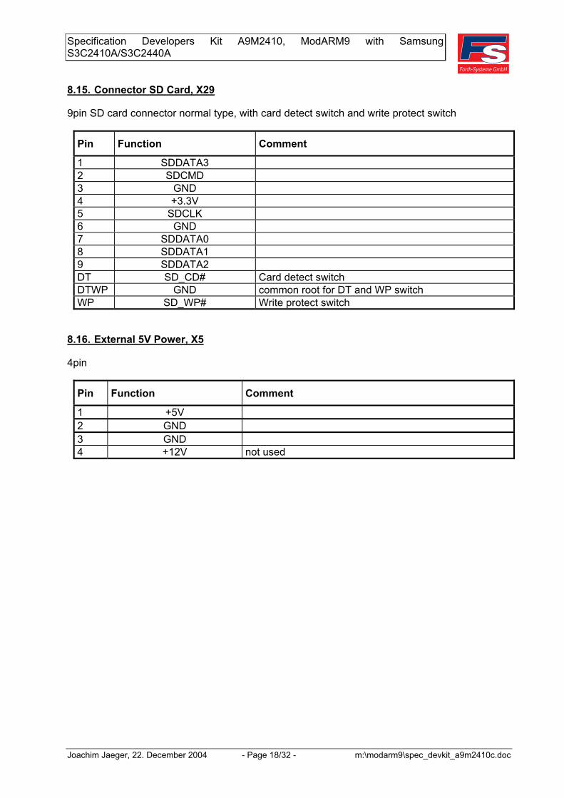
8.15. Connector SD Card, X29
9pin SD card connector normal type, with card detect switch and write protect switch
Pin Function Comment
1 SDDATA32 SDCMD3 GND4 +3.3V5 SDCLK6 GND7 SDDATA08 SDDATA19 SDDATA2DT SD_CD# Card detect switchDTWP GND common root for DT and WP switchWP SD_WP# Write protect switch
8.16. External 5V Power, X5
4pin
Pin Function Comment
1 +5V2 GND3 GND4 +12V not used
Specification Developers Kit A9M2410, ModARM9 with SamsungS3C2410A/S3C2440A
Joachim Jaeger, 22. December 2004 - Page 19/32 - m:\modarm9\spec_devkit_a9m2410c.doc
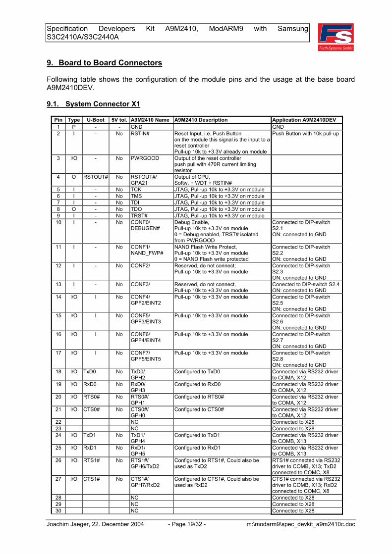
9. Board to Board Connectors
Following table shows the configuration of the module pins and the usage at the base boardA9M2410DEV.
9.1. System Connector X1
Pin Type U-Boot 5V tol. A9M2410 Name A9M2410 Description Application A9M2410DEV1 P - - GND GND2 I - No RSTIN# Reset Input, i.e. Push Button
on the module this signal is the input to areset controllerPull-up 10k to +3.3V already on module
Push Button with 10k pull-up
3 I/O - No PWRGOOD Output of the reset controllerpush pull with 470R current limitingresistor
4 O RSTOUT# No RSTOUT#/GPA21
Output of CPU,Softw. + WDT + RSTIN#
5 I - No TCK JTAG, Pull-up 10k to +3.3V on module 6 I - No TMS JTAG, Pull-up 10k to +3.3V on module7 I - No TDI JTAG, Pull-up 10k to +3.3V on module8 O - No TDO JTAG, Pull-up 10k to +3.3V on module9 I - No TRST# JTAG, Pull-up 10k to +3.3V on module
10 I - No CONF0/DEBUGEN#
Debug Enable,Pull-up 10k to +3.3V on module0 = Debug enabled, TRST# isolatedfrom PWRGOOD
Connected to DIP-switchS2.1ON: connected to GND
11 I - No CONF1/NAND_FWP#
NAND Flash Write Protect,Pull-up 10k to +3.3V on module0 = NAND Flash write protected
Connected to DIP-switchS2.2ON: connected to GND
12 I - No CONF2/ Reserved, do not connect;Pull-up 10k to +3.3V on module
Connected to DIP-switchS2.3ON: connected to GND
13 I - No CONF3/ Reserved, do not connect,Pull-up 10k to +3.3V on module
Conected to DIP-switch S2.4ON: connected to GND
14 I/O I No CONF4/GPF2/EINT2
Pull-up 10k to +3.3V on module Connected to DIP-switchS2.5ON: connected to GND
15 I/O I No CONF5/GPF3/EINT3
Pull-up 10k to +3.3V on module Connected to DIP-switchS2.6ON: connected to GND
16 I/O I No CONF6/GPF4/EINT4
Pull-up 10k to +3.3V on module Connected to DIP-switchS2.7ON: connected to GND
17 I/O I No CONF7/GPF5/EINT5
Pull-up 10k to +3.3V on module Connected to DIP-switchS2.8ON: connected to GND
18 I/O TxD0 No TxD0/GPH2
Configured to TxD0 Connected via RS232 driverto COMA, X12
19 I/O RxD0 No RxD0/GPH3
Configured to RxD0 Connected via RS232 driverto COMA, X12
20 I/O RTS0# No RTS0#/GPH1
Configured to RTS0# Connected via RS232 driverto COMA, X12
21 I/O CTS0# No CTS0#/GPH0
Configured to CTS0# Connected via RS232 driverto COMA, X12
22 NC Connected to X2823 NC Connected to X2824 I/O TxD1 No TxD1/
GPH4Configured to TxD1 Connected via RS232 driver
to COMB, X1325 I/O RxD1 No RxD1/
GPH5Configured to RxD1 Connected via RS232 driver
to COMB, X1326 I/O RTS1# No RTS1#/
GPH6/TxD2Configured to RTS1#, Could also beused as TxD2
RTS1# connected via RS232driver to COMB, X13; TxD2connected to COMC, X8
27 I/O CTS1# No CTS1#/GPH7/RxD2
Configured to CTS1#, Could also beused as RxD2
CTS1# connected via RS232driver to COMB, X13; RxD2connected to COMC, X8
28 NC Connected to X2829 NC Connected to X2830 NC Connected to X28
Specification Developers Kit A9M2410, ModARM9 with SamsungS3C2410A/S3C2440A
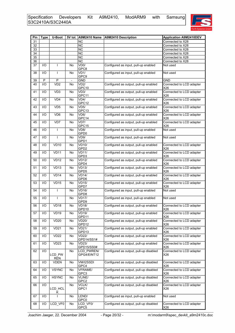
Joachim Jaeger, 22. December 2004 - Page 20/32 - m:\modarm9\spec_devkit_a9m2410c.doc
Pin Type U-Boot 5V tol. A9M2410 Name A9M2410 Description Application A9M2410DEV31 NC Connected to X2832 NC Connected to X2833 NC Connected to X2834 NC Connected to X2835 NC Connected to X2836 NC Connected to X2837 I/O I No VD0/
GPC8Configured as input, pull-up enabled Not used
38 I/O I No VD1/GPC9
Configured as input, pull-up enabled Not used
39 P P - GND GND40 I/O VD2 No VD2/
GPC10Configured as output, pull-up enabled Connected to LCD adapter
X2641 I/O VD3 No VD3/
GPC11Configured as output, pull-up enabled Connected to LCD adapter
X2642 I/O VD4 No VD4/
GPC12Configured as output, pull-up enabled Connected to LCD adapter
X2643 I/O VD5 No VD5/
GPC13Configured as output, pull-up enabled Connected to LCD adapter
X2644 I/O VD6 No VD6/
GPC14Configured as output, pull-up enabled Connected to LCD adapter
X2645 I/O VD7 No VD7/
GPC15Configured as output, pull-up enabled Connected to LCD adapter
X2646 I/O I No VD8/
GPD0Configured as input, pull-up enabled Not used
47 I/O I No VD9/GPD1
Configured as input, pull-up enabled Not used
48 I/O VD10 No VD10/GPD2
Configured as output, pull-up enabled Connected to LCD adapterX26
49 I/O VD11 No VD11/GPD3
Configured as output, pull-up enabled Connected to LCD adapterX26
50 I/O VD12 No VD12/GPD4
Configured as output, pull-up enabled Connected to LCD adapterX26
51 I/O VD13 No VD13/GPD5
Configured as output, pull-up enabled Connected to LCD adapterX26
52 I/O VD14 No VD14/GPD6
Configured as output, pull-up enabled Connected to LCD adapterX26
53 I/O VD15 No VD15/GPD7
Configured as output, pull-up enabled Connected to LCD adapterX26
54 I/O I No VD16/GPD8
Configured as input, pull-up enabled Not used
55 I/O I No VD17/GPD9
Configured as input, pull-up enabled Not used
56 I/O VD18 No VD18/GPD10
Configured as output, pull-up enabled Connected to LCD adapterX26
57 I/O VD19 No VD19/GPD11
Configured as output, pull-up enabled Connected to LCD adapterX26
58 I/O VD20 No VD20/GPD12
Configured as output, pull-up enabled Connected to LCD adapterX26
59 I/O VD21 No VD21/GPD13
Configured as output, pull-up enabled Connected to LCD adapterX26
60 I/O VD22 No VD22/GPD14/SS1#
Configured as output, pull-up enabled Connected to LCD adapterX26
61 I/O VD23 No VD23/GPD15/SS0#
Configured as output, pull-up enabled Connected to LCD adapterX26
62 I/OLCD_PW
REN
No LCD_PWREN/GPG4/EINT12
Configured as output, pull-up disabled Connected to LCD adapterX26
63 I/O VDEN No VM/I2SSDIGPC4
Configured as output, pull-up disabled Connected to LCD adapterX26
64 I/O VSYNC No VFRAME/GPC3
Configured as output, pull-up disabled Connected to LCD adapterX26
65 I/O HSYNC No VLINE/GPC2
Configured as output, pull-up disabled Connected to LCD adapterX26
66 I/OLCD_HCL
K
No VCLK/GPC1
Configured as output, pull-up disabled Connected to LCD adapterX26
67 I/O I No LEND/GPC0
Configured as input, pull-up enabled Not used
68 I/O LCD_VF0 No LCD_VF0/GPC5
Configured as output, pull-up disabled Connected to LCD adapterX26
Specification Developers Kit A9M2410, ModARM9 with SamsungS3C2410A/S3C2440A
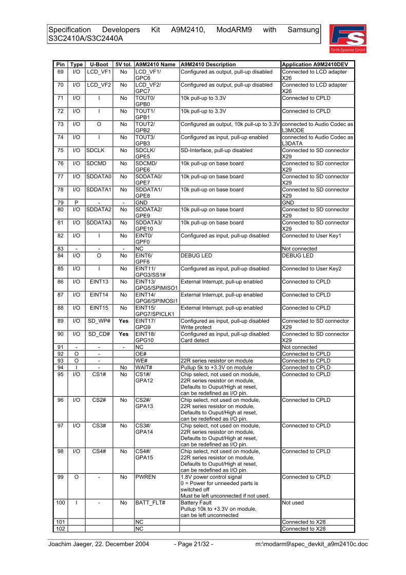
Joachim Jaeger, 22. December 2004 - Page 21/32 - m:\modarm9\spec_devkit_a9m2410c.doc
Pin Type U-Boot 5V tol. A9M2410 Name A9M2410 Description Application A9M2410DEV69 I/O LCD_VF1 No LCD_VF1/
GPC6Configured as output, pull-up disabled Connected to LCD adapter
X2670 I/O LCD_VF2 No LCD_VF2/
GPC7Configured as output, pull-up disabled Connected to LCD adapter
X2671 I/O I No TOUT0/
GPB010k pull-up to 3.3V Connected to CPLD
72 I/O I No TOUT1/GPB1
10k pull-up to 3.3V Connected to CPLD
73 I/O O No TOUT2/GPB2
Configured as output, 10k pull-up to 3.3V connected to Audio Codec asL3MODE
74 I/O I No TOUT3/GPB3
Configured as input, pull-up enabled connected to Audio Codec asL3DATA
75 I/O SDCLK No SDCLK/GPE5
SD-Interface, pull-up disabled Connected to SD connectorX29
76 I/O SDCMD No SDCMD/GPE6
10k pull-up on base board Connected to SD connectorX29
77 I/O SDDATA0 No SDDATA0/GPE7
10k pull-up on base board Connected to SD connectorX29
78 I/O SDDATA1 No SDDATA1/GPE8
10k pull-up on base board Connected to SD connectorX29
79 P - - GND GND80 I/O SDDATA2 No SDDATA2/
GPE910k pull-up on base board Connected to SD connector
X2981 I/O SDDATA3 No SDDATA3/
GPE1010k pull-up on base board Connected to SD connector
X2982 I/O I No EINT0/
GPF0Configured as input, pull-up disabled Connected to User Key1
83 - - - NC Not connected84 I/O O No EINT6/
GPF6DEBUG LED DEBUG LED
85 I/O I No EINT11/GPG3/SS1#
Configured as input, pull-up disabled Connected to User Key2
86 I/O EINT13 No EINT13/GPG5/SPIMISO1
External Interrupt, pull-up enabled Connected to CPLD
87 I/O EINT14 No EINT14/GPG6/SPIMOSI1
External Interrupt, pull-up enabled Connected to CPLD
88 I/O EINT15 No EINT15/GPG7/SPICLK1
External Interrupt, pull-up enabled Connected to CPLD
89 I/O SD_WP# Yes EINT17/GPG9
Configured as input, pull-up disabledWrite protect
Connected to SD connectorX29
90 I/O SD_CD# Yes EINT18/GPG10
Configured as input, pull-up disabledCard detect
Connected to SD connectorX29
91 - - - NC Not connected92 O - OE# Connected to CPLD93 O - WE# 22R series resistor on module Connected to CPLD94 I - No WAIT# Pullup 5k to +3.3V on module Connected to CPLD95 I/O CS1# No CS1#/
GPA12Chip select, not used on module,22R series resistor on module, Defaults to Ouput/High at reset,can be redefined as I/O pin.
Connected to CPLD
96 I/O CS2# No CS2#/GPA13
Chip select, not used on module,22R series resistor on module,Defaults to Ouput/High at reset,can be redefined as I/O pin.
Connected to CPLD
97 I/O CS3# No CS3#/GPA14
Chip select, not used on module,22R series resistor on module,Defaults to Ouput/High at reset,can be redefined as I/O pin.
Connected to CPLD
98 I/O CS4# No CS4#/GPA15
Chip select, not used on module,22R series resistor on module,Defaults to Ouput/High at reset,can be redefined as I/O pin.
Connected to CPLD
99 O - No PWREN 1.8V power control signal0 = Power for unneeded parts isswitched offMust be left unconnected if not used.
Connected to CPLD
100 I - No BATT_FLT# Battery FaultPullup 10k to +3.3V on module, can be left unconnected
Not used
101 NC Connected to X28102 NC Connected to X28
Specification Developers Kit A9M2410, ModARM9 with SamsungS3C2410A/S3C2440A
Joachim Jaeger, 22. December 2004 - Page 22/32 - m:\modarm9\spec_devkit_a9m2410c.doc
Pin Type U-Boot 5V tol. A9M2410 Name A9M2410 Description Application A9M2410DEV103 O - No DQM0 Upper Byte/Lower Byte Enable Connected to CPLD104 O - No DQM1 Connected to CPLD105 O - No DQM2 Not used106 O - No DQM3 Not used107 I/O SS0# No SS0#
GPG2/EINT10SPI0, pull-up enabled Not used
108 I/OSPIMISO0
No SPIMISO0GPE11
Pull-up enabled Not used
109 I/OSPIMOSI0
No SPIMOSI0GPE12
Pull-up enabled Not used
110 I/O SPICLK0 No SPICLK0GPE13
Pull-up disabled Not used
111 I/O IICSCL No IICSCLGPE14
I²C clock, Pullup 4k7 to 3.3V on module used on module,
112 I/O IICSDA No IICSDAGPE15
I²C data, Pullup 4k7 to 3.3V on module used on module
113 I/O O No USB_DT/PWGPG0/EINT8
USB Detect/PowerEnable, by default setto output, pull-up enabled
output to switch on 1k5 pull-up resistor for USB device
114 I/O USBP YES USBP USB device, 22R series resistor has tobe mounted on base board
USB device data line +,connected to X15
115 I/O USBN YES USBN USB device, 22R series resistor has tobe mounted on base board
USB device data line -,connected to X15
116 P - - VRTC Backup Battery for RTC, for 3V cell,power-switch-over is on the module,Can be left floating, if RTC backup notneeded.
3V battery connected
117 P - - GND GND118 P - - +3.3V +3.3V119 P - - VLIO Mobile: Power from Li-Ion Battery
Non-Mobile: connected to 3.3VDelivers either power from Li-Ion battery or 3.3V
120 P - - +3.3V +3.3V
Specification Developers Kit A9M2410, ModARM9 with SamsungS3C2410A/S3C2440A
Joachim Jaeger, 22. December 2004 - Page 23/32 - m:\modarm9\spec_devkit_a9m2410c.doc
9.2. System Connector X2
Pin Type U-Boot 5V tol. A9M2410 Name A9M2410 Description Application A9M2410DEV1 I/O USBP0 Yes USBP0 USB host0, 22R series resistor has to be
mounted on base boardUSB host data line +,connected to X14
2 P - - GND GND3 I/O USBN0 Yes USBN0 USB host0, 22R series resistor has to be
mounted on base boardUSB host data line -,connected to X14
4 O A0 No A0/GPA0 used as address of ETH-Contr. onmodule,should not be used as I/O pin forcompatibility
Connected to CPLD
5 O - No A1 Connected to CPLD6 O - No A2 Connected to CPLD7 O - No A3 Connected to CPLD8 O - No A4 Connected to CPLD9 O - No A5 Connected to CPLD
10 O - No A6 Connected to CPLD11 O - No A7 Connected to CPLD12 O - No A8 Connected to CPLD13 O - No A9 Connected to CPLD14 O - No A10 Connected to CPLD15 O - No A11 Connected to CPLD16 O - No A12 Connected to CPLD17 O - No A13 Not used18 O - No A14 Not used19 O - No A15 Not used20 O A16 No A16/GPA1 used as address of ETH-Contr. on
module,should not be used as I/O pin forcompatibility
Not used
21 O A17 No A17/GPA2 used as address of ETH-Contr. onmodule,should not be used as I/O pin forcompatibility
Not used
22 O A18 No A18/GPA3 used as address of ETH-Contr. onmodule,should not be used as I/O pin forcompatibility
Not used
23 O A19 No A19/GPA4 used as address of ETH-Contr. onmodule,should not be used as I/O pin forcompatibility
Not used
24 O A20 No A20/GPA5 should not be used as I/O pin forcompatibility
Not used
25 O A21 No A21/GPA6 should not be used as I/O pin forcompatibility
Not used
26 O A22 No A22/GPA7 should not be used as I/O pin forcompatibility
Not used
27 O A23 No A23/GPA8 should not be used as I/O pin forcompatibility
Connected to CPLD
28 O A24 No A24/GPA9 should not be used as I/O pin forcompatibility
Not used
29 O A25 No A25/GPA10 should not be used as I/O pin forcompatibility
Not used
30 O A26 No A26/GPA11 should not be used as I/O pin forcompatibility
Not used
31 - - - Reserved (A27) Not connected32 - - - Reserved (A28) Not connected33 - - - Reserved (A29) Not connected34 - - - Reserved (A30) Not connected35 - - - Reserved (A31) Not connected36 I/O I No XDREQ0#/
GPB10Configured as input, pull-up enabled Not used
37 I/O I No XDREQ1#/GPB8
Configured as input, pull-up enabled Not used
38 I/O I No XDACK0#/GPB9
Configured as input, pull-up enabled Not used
39 I/O I No XDACK1#/GPB7
Configured as input, pull-up enabled Not used
40 P - - GND GND
Specification Developers Kit A9M2410, ModARM9 with SamsungS3C2410A/S3C2440A
Joachim Jaeger, 22. December 2004 - Page 24/32 - m:\modarm9\spec_devkit_a9m2410c.doc
Pin Type U-Boot 5V tol. A9M2410 Name A9M2410 Description Application A9M2410DEV41 - - - NC - Not connected42 - - - NC - Not connected43 AI - No AIN0 Analog in,
unused analog inputs should beconnected to AGND over a 10k seriesresistor to avoid cross over.
Not used
44 AI - No AIN1 Not used45 AI - No AIN2 Not used46 AI - No AIN3 Not used47 AI - No AIN4 Used for touch screen TSYM Connected to Touch screen
connector X2748 AI - No AIN5 Used for touch screen TSYP Connected to Touch screen
connector X2749 AI - No AIN6 Used for touch screen TSXM Connected to Touch screen
connector X2750 AI - No AIN7 Used for touch screen TSXP Connected to Touch screen
connector X2751 REF - No AVCC Analog VCC,
Is the extra filtered +3.3V,connected with the AVCC ball of theCPUCan be used as an analog reference,do not connect to any other powersource.
Not used
52 REF - No AGND Analog GND,Is the extra filtered GND,connected with the AGND ball of theCPU,Can be used as an analog reference,do not connect to any other powersource.
Connected to Touch screenconnector X27
53 I/O XPON# No XPON#/GPG13/EINT21
Touch Screen, pull-up disabled Used for touch screen
54 I/O XMON No XMON/GPG12/EINT20
pull-up disabled Used for touch screen
55 I/O YPON# No YPON#/GPG15/EINT23
pull-up disabled Used for touch screen
56 I/O YMON No YMON/GPG14/EINT22
pull-up disabled Used for touch screen
57 I/O I No XBREQ#/GPB6
Configured as input, pull-up enabled Not used
58 I/O I No XBACK#/GPB5
Configured as input, pull-up enabled Not used
59 I/O I Yes USBH0PEN/GPG8/EINT16
USB host0 Power Enable USB host: input to recognizecurrent limit from connecteddevice
60 - - NC Not connected61 I/O I2SSDO No I2SSDO/
GPE4/I2SSDII2S-Interface, pull-up disabled Connected to Audio Codec
62 I/O I2SSDI No I2SSDI/GPE3/SS0#
pull-up disabled Connected to Audio Codec
63 I/O CDCLK No CDCLK/GPE2
pull-up disabled Connected to Audio Codec
64 I/O I2SSCLK No I2SSCLK/GPE1
pull-up disabled Connected to Audio Codec
65 I/O I2SLRCK No I2SLRCK/GPE0
pull-up disabled Connected to Audio Codec
66 I - No TPIN Ethernet 0 Input-,100R differential termination on module
Connected to RJ45 withintegrated magnetics
67 O - No LEDLNK Ethernet 0 Line/Activity LEDHigh, when link okLow, while active.
Connected to Link/ActivityLED
68 I - No TPIP Ethernet 0 Input+,100R differential termination on module
Connected to RJ45 withintegrated magnetics
69 O - No not used reserved for high speed LED Not connected70 O - No TPON Ethernet 0 Output-,
100R differential termination on moduleConnected to RJ45 withintegrated magnetics
71 I - No not used Not connected72 O - No TPOP Ethernet 0 Output+,
100R differential termination on moduleConnected to RJ45 withintegrated magnetics
73 P - Not used Not connected74 - - - Reserved Not connected
Specification Developers Kit A9M2410, ModARM9 with SamsungS3C2410A/S3C2440A
Joachim Jaeger, 22. December 2004 - Page 25/32 - m:\modarm9\spec_devkit_a9m2410c.doc
Pin Type U-Boot 5V tol. A9M2410 Name A9M2410 Description Application A9M2410DEV75 - - - Reserved Not connected76 - - - Reserved Not connected77 - - - Reserved Not connected78 - - - Reserved Not connected79 - - - Reserved Not connected80 P - - GND GND81 I/O - No D0 Data Bus Connected to CPLD82 I/O - No D1 Connected to CPLD83 I/O - No D2 Connected to CPLD84 I/O - No D3 Connected to CPLD85 I/O - No D4 Connected to CPLD86 I/O - No D5 Connected to CPLD87 I/O - No D6 Connected to CPLD88 I/O - No D7 Connected to CPLD89 I/O - No D8 Connected to CPLD90 I/O - No D9 Connected to CPLD91 I/O - No D10 Connected to CPLD92 I/O - No D11 Connected to CPLD93 I/O - No D12 Connected to CPLD94 I/O - No D13 Connected to CPLD95 I/O - No D14 Connected to CPLD96 I/O - No D15 Connected to CPLD97 I/O - No D16 Not used98 I/O - No D17 Not used99 I/O - No D18 Not used
100 I/O - No D19 Not used101 I/O - No D20 Not used102 I/O - No D21 Not used103 I/O - No D22 Not used104 I/O - No D23 Not used105 I/O - No D24 Not used106 I/O - No D25 Not used107 I/O - No D26 Not used108 I/O - No D27 Not used109 I/O - No D28 Not used110 I/O - No D29 Not used111 I/O - No D30 Not used112 I/O - No D31 Not used113 I/O O No TCLK0/
GPB4Configured as output, pull-up enabled connected to Audio Codec as
L3CLOCK114 I/O I No TCLK1/
GPG11/EINT19Configured as input, pull-up enabled Not used
115 - - - NC - Not connected116 O CLKOUT1 No CLKOUT1/
GPH10Clock output, unbuffered CLKOUT1signal, 22R series resistor on module
Connected to CPLD via 0Rbut 0R resistor not equipped
117 - - - NC - Connected to CAN driver118 - - - NC - Connected to CAN driver119 O CLKOUT0 No BCLKOUT0/
GPH9Clock output, buffered CLKOUT0 signal Connected to CPLD
120 P - - GND - GND
AI: Analog InputI: InputO: OutputI/O: Input or OutputP: PowerREF: Analog Reference Voltage

Specification Developers Kit A9M2410, ModARM9 with SamsungS3C2410A/S3C2440A
Joachim Jaeger, 22. December 2004 - Page 26/32 - m:\modarm9\spec_devkit_a9m2410c.doc
9.3. System Connector X3
Pin Signal Type Signal Name Description X3-1 GND P GNDX3-2X3-3X3-4X3-5X3-6X3-7X3-8X3-9X3-10X3-11X3-12X3-13X3-14X3-15X3-16X3-17X3-18X3-19X3-20X3-21X3-22X3-23X3-24X3-25X3-26X3-27X3-28X3-29X3-30X3-31 GND P GNDX3-32X3-33X3-34X3-35X3-36X3-37X3-38X3-39X3-40X3-41X3-42X3-43X3-44X3-45X3-46X3-47X3-48X3-49
Specification Developers Kit A9M2410, ModARM9 with SamsungS3C2410A/S3C2440A
Joachim Jaeger, 22. December 2004 - Page 27/32 - m:\modarm9\spec_devkit_a9m2410c.doc
Pin Signal Type Signal Name Description X3-50X3-51X3-52X3-53X3-54X3-55X3-56X3-57X3-58X3-59 GND P GNDX3-60
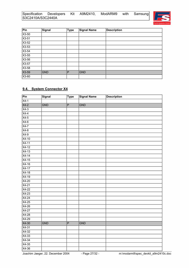
9.4. System Connector X4
Pin Signal Type Signal Name Description X4-1X4-2 GND P GNDX4-3X4-4X4-5X4-6X4-7X4-8X4-9X4-10X4-11X4-12X4-13X4-14X4-15X4-16X4-17X4-18X4-19X4-20X4-21X4-22X4-23X4-24X4-25X4-26X4-27X4-28X4-29X4-30 GND P GNDX4-31X4-32X4-33X4-34X4-35X4-36
Specification Developers Kit A9M2410, ModARM9 with SamsungS3C2410A/S3C2440A
Joachim Jaeger, 22. December 2004 - Page 28/32 - m:\modarm9\spec_devkit_a9m2410c.doc
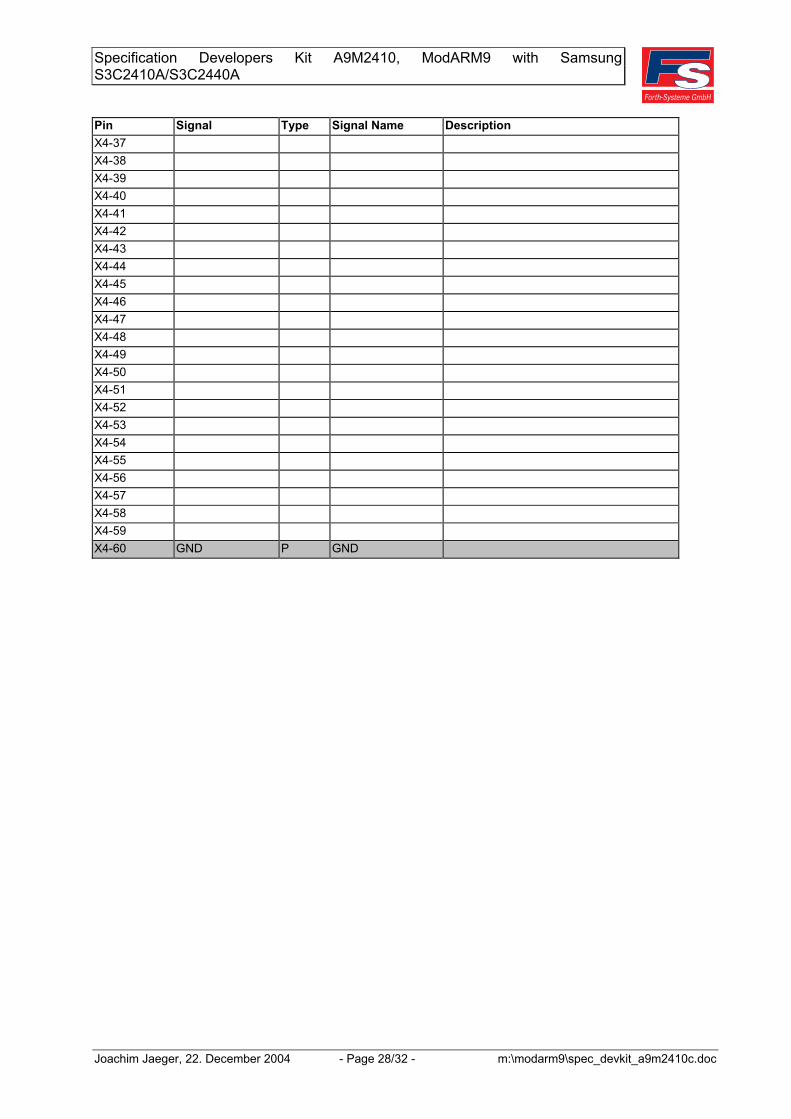
Pin Signal Type Signal Name Description X4-37X4-38X4-39X4-40X4-41X4-42X4-43X4-44X4-45X4-46X4-47X4-48X4-49X4-50X4-51X4-52X4-53X4-54X4-55X4-56X4-57X4-58X4-59X4-60 GND P GND

Specification Developers Kit A9M2410, ModARM9 with SamsungS3C2410A/S3C2440A
Joachim Jaeger, 22. December 2004 - Page 29/32 - m:\modarm9\spec_devkit_a9m2410c.doc
10. Appendix A: Expansion Connectors
10.1. Module Connector X1 versus Expansion Connectors X10/X11
Pin X10, Row A X10, Row B X11, Row C X11, Row D
1 GND RSTIN# PWRGOOD RSTOUT#2 TCK TMS TDI TDO3 TRST# DEBUGEN# NAND_FWP# CONF24 CONF3 CONF4 CONF5 CONF65 CONF7 TXD0 RXD0 RTS0#6 CTS0# nc nc TXD17 RXD1 RTS1# CTS1# nc8 PLD_I/O0 PLD_I/O1 PLD_I/O2 PLD_I/O39 PLD_I/O4 PLD_I/O5 PLD_I/O6 PLD_I/O7
10 VD0 VD1 GND VD211 VD3 VD4 VD5 VD612 VD7 VD8 VD9 VD1013 VD11 VD12 VD13 VD1414 VD15 VD16 VD17 VD1815 VD19 VD20 VD21 VD2216 VD23 LCD_PWREN VDEN VSYNC17 HSYNC LCD_HCLK LEND LCDVF018 LCDVF1 LCDVF2 TOUT0 TOUT119 L3MODE L3DATA SDCLK SDCMD20 SDDATA0 SDDATA1 GND SDDATA221 SDDATA3 USER_KEY1 nc DEBUG_LED22 USER_KEY2 EINT13 EINT14 EINT1523 SD_WP# SD_CD# nc OE#24 WE# WAIT# CS1# CS2#25 CS3# CS4# PWREN BATT_FLT#26 nc nc DQM0 DQM127 DQM2 DQM3 SS0# SPIMISO028 SPIMOSI0 SPICLK0 IICSCL IICSDA29 USB_DT/PW USBP USBN VRTC30 GND GND VLIO VLIO31 nc nc nc nc32 +3.3V +3.3V +3.3V +3.3V

Specification Developers Kit A9M2410, ModARM9 with SamsungS3C2410A/S3C2440A
Joachim Jaeger, 22. December 2004 - Page 30/32 - m:\modarm9\spec_devkit_a9m2410c.doc
10.2. Module Connector X2 versus Expansion Connectors X20/X21
Pin X20, Row A X20, Row B X21, Row C X21, Row D
1 USBP0 GND USBN0 A02 A1 A2 A3 A43 A5 A6 A7 A84 A9 A10 A11 A125 A13 A14 A15 A166 A17 A18 A19 A207 A21 A22 A23 A248 A25 A26 nc nc9 nc nc nc XDREQ0#
10 XDREQ1# XDACK0# XDACK1# GND11 nc nc AIN0 AIN112 AIN2 AIN3 AIN4 AIN513 AIN6 AIN7 AVCC AGND14 XPON# XMON YPON# YMON15 XBREQ# XBACK# USBH0PEN nc16 I2SSDO I2SSDI CDCLK I2SSCLK17 nc nc LEDLNK I2SLRCK18 nc nc nc nc19 nc nc nc nc20 nc nc nc GND21 D0 D1 D2 D322 D4 D5 D6 D723 D8 D9 D10 D1124 D12 D13 D14 D1525 D16 D17 D18 D1926 D20 D21 D22 D2327 D24 D25 D26 D2728 D28 D29 D30 D3129 L3CLOCK TCLK1 nc CLKOUT130 nc nc BCLKOUT0 GND31 VLIO VRTC GND GND32 +3.3V +3.3V RSTIN# PWRGOOD
Specification Developers Kit A9M2410, ModARM9 with SamsungS3C2410A/S3C2440A
Joachim Jaeger, 22. December 2004 - Page 31/32 - m:\modarm9\spec_devkit_a9m2410c.doc
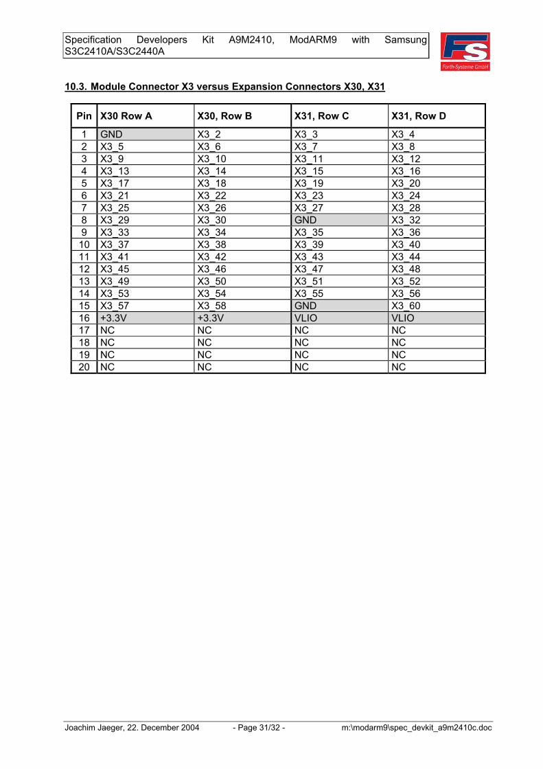
10.3. Module Connector X3 versus Expansion Connectors X30, X31
Pin X30 Row A X30, Row B X31, Row C X31, Row D
1 GND X3_2 X3_3 X3_42 X3_5 X3_6 X3_7 X3_83 X3_9 X3_10 X3_11 X3_124 X3_13 X3_14 X3_15 X3_165 X3_17 X3_18 X3_19 X3_206 X3_21 X3_22 X3_23 X3_247 X3_25 X3_26 X3_27 X3_288 X3_29 X3_30 GND X3_329 X3_33 X3_34 X3_35 X3_36
10 X3_37 X3_38 X3_39 X3_4011 X3_41 X3_42 X3_43 X3_4412 X3_45 X3_46 X3_47 X3_4813 X3_49 X3_50 X3_51 X3_5214 X3_53 X3_54 X3_55 X3_5615 X3_57 X3_58 GND X3_6016 +3.3V +3.3V VLIO VLIO17 NC NC NC NC18 NC NC NC NC19 NC NC NC NC20 NC NC NC NC

Specification Developers Kit A9M2410, ModARM9 with SamsungS3C2410A/S3C2440A
Joachim Jaeger, 22. December 2004 - Page 32/32 - m:\modarm9\spec_devkit_a9m2410c.doc
10.4. Module Connector X4 versus Expansion Connectors X40, X41
Pin X40 Row A X40, Row B X41, Row C X41, Row D
1 X4_1 GND X4_3 X4_42 X4_5 X4_6 X4_7 X4_83 X4_9 X4_10 X4_11 X4_124 X4_13 X4_14 X4_15 X4_165 X4_17 X4_18 X4_19 X4_206 X4_21 X4_22 X4_23 X4_247 X4_25 X4_26 X4_27 X4_288 X4_29 GND X4_31 X4_329 X4_33 X4_34 X4_35 X4_36
10 X4_37 X4_38 X4_39 X4_4011 X4_41 X4_42 X4_43 X4_4412 X4_45 X4_46 X4_47 X4_4813 X4_49 X4_50 X4_51 X4_5214 X4_53 X4_54 X4_55 X4_5615 X4_57 X4_58 X4_59 GND16 +3.3V +3.3V VLIO VLIO17 NC NC NC NC18 NC NC NC NC19 NC NC NC NC20 NC NC NC NC