Embed Size (px)
DESCRIPTION
The aims of the meeting are to prepare ourselves for interacting with STFC as the situation unfolds. Specifically: Review and summarise our options to optimise the science output from SPiDeR. Identify the papers which could/should be published in the next year. - PowerPoint PPT Presentation
Citation preview
Jan 13 2010 p 11
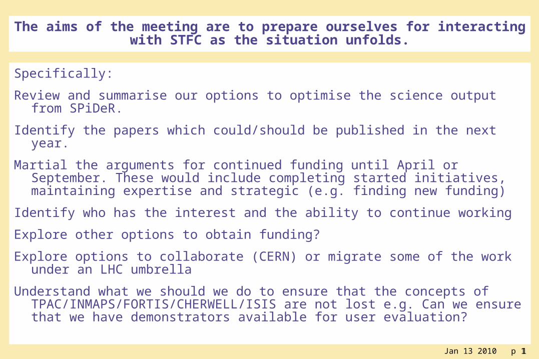
The aims of the meeting are to prepare ourselves for interacting with STFC as the situation unfolds.
Specifically:
Review and summarise our options to optimise the science output from SPiDeR.
Identify the papers which could/should be published in the next year.
Martial the arguments for continued funding until April or September. These would include completing started initiatives, maintaining expertise and strategic (e.g. finding new funding)
Identify who has the interest and the ability to continue working
Explore other options to obtain funding?
Explore options to collaborate (CERN) or migrate some of the work under an LHC umbrella
Understand what we should we do to ensure that the concepts of TPAC/INMAPS/FORTIS/CHERWELL/ISIS are not lost e.g. Can we ensure that we have demonstrators available for user evaluation?

Jan 13 2010 p 22
10:00 – 11:00 TPAC, FORTIS, CHERWELL, ISIS status reports11:00 – 11:30 Discussion and summary
The presentations should be brief (10’) recalling the investment to-date, the current status, the likely status in April and the benefit of continuing until September (or longer) i.e.
• Brief update on status of measurements and analysis
• What is still needed to complete work to publication?
• What would be the case for submitting a new prototype?
• What are the reasons to proceed with test beams at DESY, CERN
• TPAC (Paul)
• FORTIS & CHERWELL (Jaap, Jamie)
• ISIS & SOI (Gary)

Jan 13 2010 p 33
11:30 – 12:00 Other MAPs projects12:00 – 12:30 Institute plans – Pixel RD, continued involvement with ILC, CLIC
• Overview of active MAPs projects in the UK (Renato?)
• Mass Spec (Andrei)
• The international scene and prospects for continuing work e.g. collaboration, new funding (All).
• LePix, OKI SOI (Mike/Gary)
• Birmingham (Nigel)
• Bristol (Joel)
• Imperial (Paul)
• Oxford (Andrei)
• RAL (Mike, Renato)
Jan 13 2010 p 44
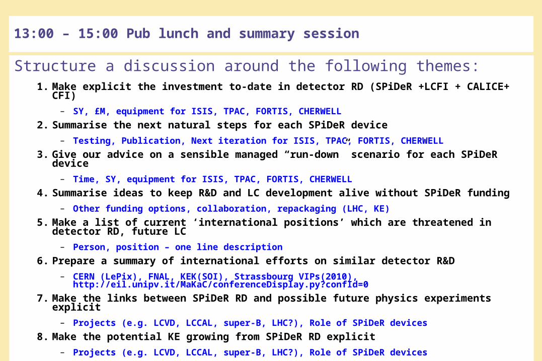
13:00 – 15:00 Pub lunch and summary session
Structure a discussion around the following themes:1. Make explicit the investment to-date in detector RD (SPiDeR +LCFI + CALICE+ CFI)
– SY, £M, equipment for ISIS, TPAC, FORTIS, CHERWELL
2. Summarise the next natural steps for each SPiDeR device
– Testing, Publication, Next iteration for ISIS, TPAC, FORTIS, CHERWELL
3. Give our advice on a sensible managed “run-down” scenario for each SPiDeR device
– Time, SY, equipment for ISIS, TPAC, FORTIS, CHERWELL
4. Summarise ideas to keep R&D and LC development alive without SPiDeR funding
– Other funding options, collaboration, repackaging (LHC, KE)
5. Make a list of current ‘international positions’ which are threatened in detector RD, future LC
– Person, position – one line description
6. Prepare a summary of international efforts on similar detector R&D
– CERN (LePix), FNAL, KEK(SOI), Strassbourg VIPs(2010), http://eil.unipv.it/MaKaC/conferenceDisplay.py?confId=0
7. Make the links between SPiDeR RD and possible future physics experiments explicit
– Projects (e.g. LCVD, LCCAL, super-B, LHC?), Role of SPiDeR devices
8. Make the potential KE growing from SPiDeR RD explicit
– Projects (e.g. LCVD, LCCAL, super-B, LHC?), Role of SPiDeR devices

Jan 13 2010 p 55
Backup: Advisory panel chairs’ letter to Drayson (12/01/10)
….extract– the waste of much of the significant prior investment made by the UK in forefront science;
– the loss of hard-won UK leadership in many significant areas;
– the lack of opportunity for developing future UK strategic opportunities for advancing the scientific frontier, with relevant knowledge exchange impact, on the 10-20 year horizon;
– the extremely negative message to bright young people about the importance the UK places in cutting-edge, fundamental science, and the career opportunities that follow from training in these areas.
Jan 13 2010 p 66
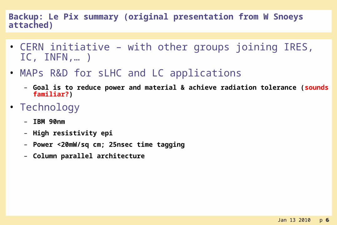
Backup: Le Pix summary (original presentation from W Snoeys attached)
• CERN initiative – with other groups joining IRES, IC, INFN,… )
• MAPs R&D for sLHC and LC applications– Goal is to reduce power and material & achieve radiation tolerance (sounds familiar?)
• Technology– IBM 90nm
– High resistivity epi
– Power <20mW/sq cm; 25nsec time tagging
– Column parallel architecture
Jan 13 2010 p 77
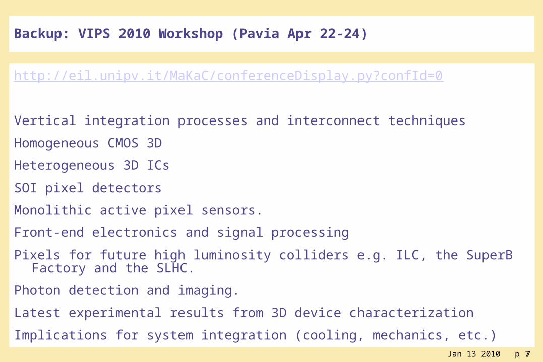
Backup: VIPS 2010 Workshop (Pavia Apr 22-24)
http://eil.unipv.it/MaKaC/conferenceDisplay.py?confId=0
Vertical integration processes and interconnect techniques
Homogeneous CMOS 3D
Heterogeneous 3D ICs
SOI pixel detectors
Monolithic active pixel sensors.
Front-end electronics and signal processing
Pixels for future high luminosity colliders e.g. ILC, the SuperB Factory and the SLHC.
Photon detection and imaging.
Latest experimental results from 3D device characterization
Implications for system integration (cooling, mechanics, etc.)
Jan 13 2010 p 88
Monolithic pixels for Silicon Tracker Upgrades
December 2009
Walter Snoeys
CERNPH-ESE-ME
1211 Geneva 23, Switzerland

Jan 13 2010 p 99
ACKNOWLEDGEMENTS
Collegues in ESE group and Alice Pixel, LHCb RICH, NA57, WA97, RD19, TOTEM Collaborations
S. Parker, C. Kenney, C.H. Aw, G. Rosseel, J.Plummer K. Kloukinas, M. Caselle, A. Marchioro, A Rivetti, V. Manzari, D. Bisello, A. Dorokhov, C. Hu,
C. Colledani, M. Winter, P. Chalmet, H. Mugnier, J. Rousset
Jan 13 2010 p 1010
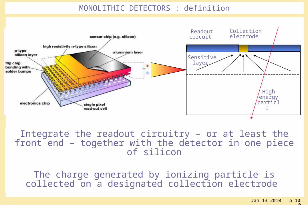
MONOLITHIC DETECTORS : definition
Integrate the readout circuitry – or at least the front end – together with the detector in one piece of silicon
The charge generated by ionizing particle is collected on a designated collection electrode
Readout circuit
Collection electrode
Sensitive layer
High energy particle
Jan 13 2010 p 1111
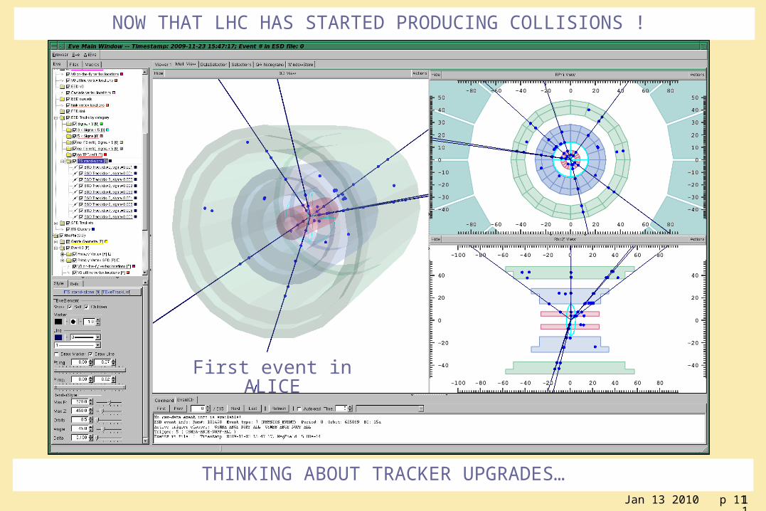
THINKING ABOUT TRACKER UPGRADES…
NOW THAT LHC HAS STARTED PRODUCING COLLISIONS !
First event in ALICE
Walter Snoeys – CERN – PH – ESE – ME-2009 12
Click to edit the outline text format
Second Outline Level Third Outline Level
Fourth Outline Level Fifth Outline Level Sixth Outline Level Seventh Outline
Level Eighth Outline
Level Ninth Outline LevelClick to edit
Master text styles Second level
Third level Fourth level
Fifth level
Click to edit the outline text format
Second Outline Level Third Outline Level
Fourth Outline Level Fifth Outline Level Sixth Outline Level Seventh Outline
Level Eighth Outline
Level Ninth Outline LevelClick to edit
Master text styles Second level
Third level Fourth level
Fifth level
Click to edit the outline text format
Second Outline Level Third Outline Level
Fourth Outline Level Fifth Outline Level Sixth Outline Level Seventh Outline
Level Eighth Outline
Level Ninth Outline LevelClick to edit
Master text styles Second level
Third level Fourth level
Fifth level
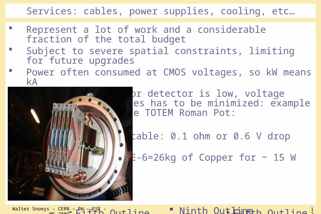
Represent a lot of work and a considerable fraction of the total budget
Subject to severe spatial constraints, limiting for future upgrades Power often consumed at CMOS voltages, so kW means kA
Even if power for detector is low, voltage drop in the cables has to be minimized: example analog supply one TOTEM Roman Pot:
~ 6A @ 2.5 V ~100m 2x16mm2 cable: 0.1 ohm or 0.6 V drop one way 8230kg*2*100*16E-6=26kg of Copper for ~ 15 W
Services: cables, power supplies, cooling, etc…
Walter Snoeys – CERN – PH – ESE – ME-2009 13
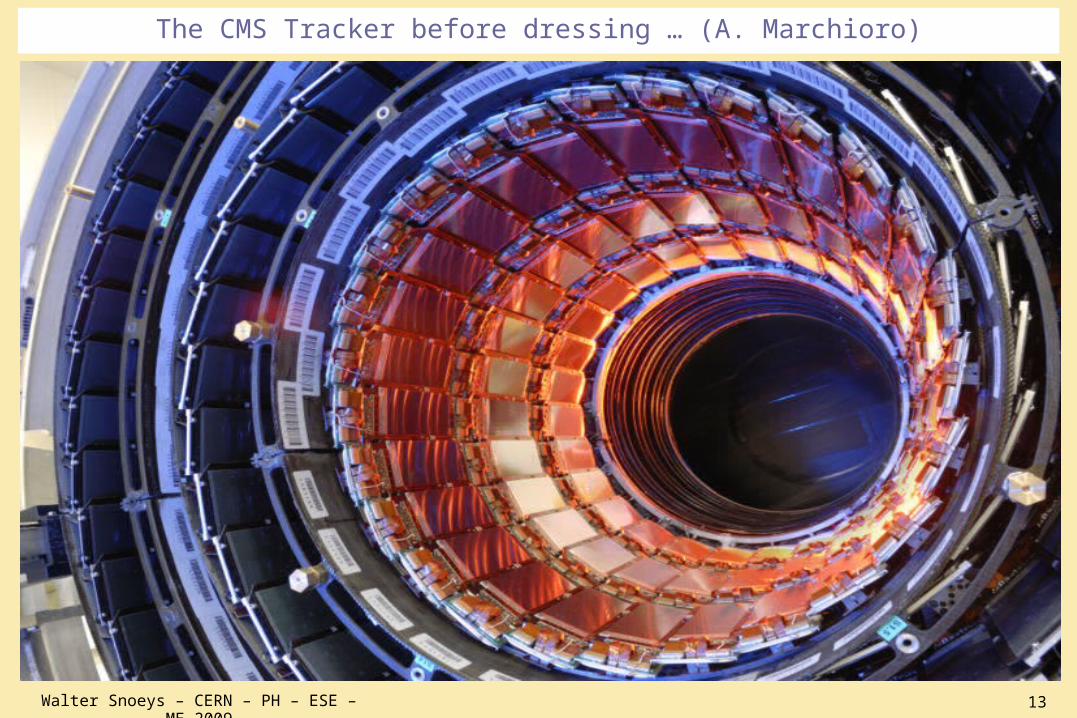
The CMS Tracker before dressing … (A. Marchioro)
Walter Snoeys – CERN – PH – ESE – ME-2009 14
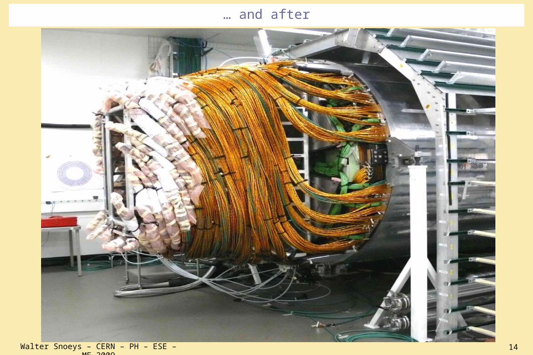
… and after
Walter Snoeys – CERN – PH – ESE – ME-2009 15

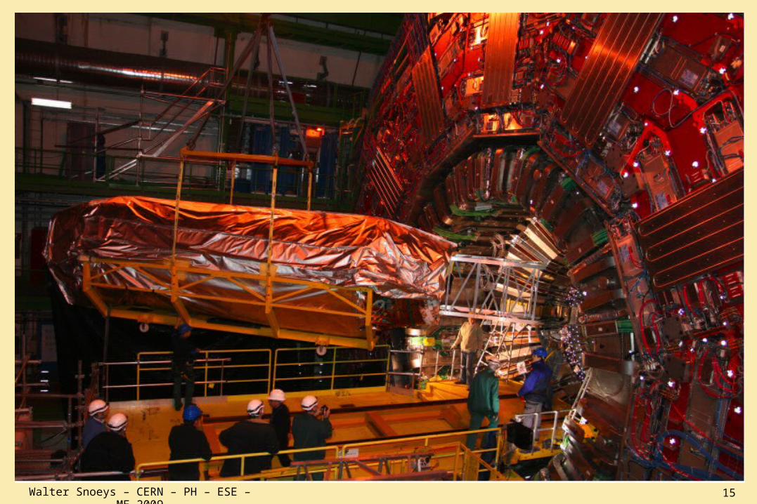
Walter Snoeys – CERN – PH – ESE – ME-2009 16
Walter Snoeys – CERN – PH – ESE – ME-2009 17
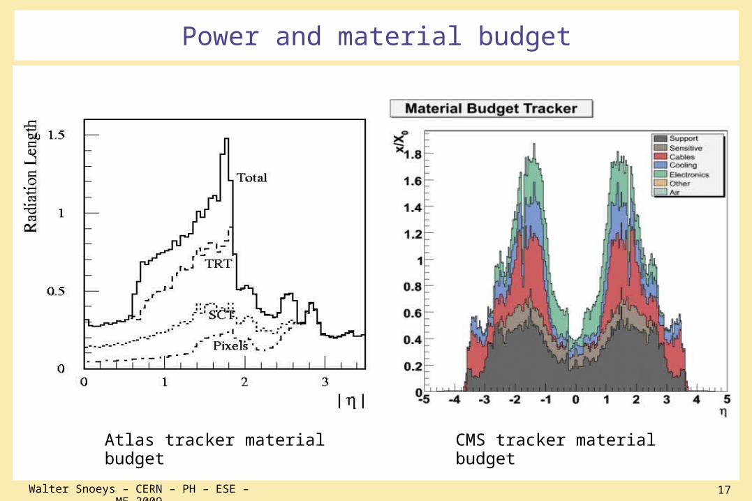
Power and material budget
Atlas tracker material budget CMS tracker material budget
Walter Snoeys – CERN – PH – ESE – ME-2009 18
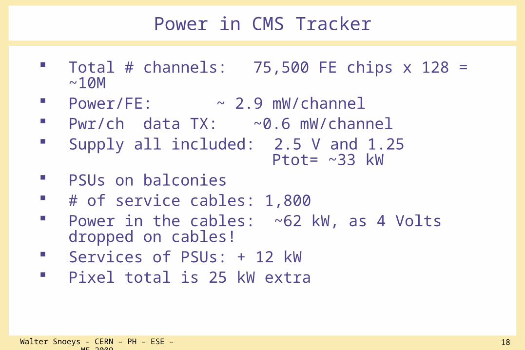
Power in CMS Tracker
Total # channels: 75,500 FE chips x 128 = ~10M Power/FE: ~ 2.9 mW/channel Pwr/ch data TX: ~0.6 mW/channel Supply all included: 2.5 V and 1.25
Ptot= ~33 kW PSUs on balconies # of service cables: 1,800 Power in the cables: ~62 kW, as 4 Volts dropped on cables! Services of PSUs: + 12 kW Pixel total is 25 kW extra
Walter Snoeys – CERN – PH – ESE – ME-2009 19
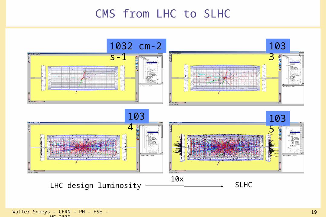
CMS from LHC to SLHC
1033
1035
1032 cm-2 s-1
1034
LHC design luminosity SLHC10x

Jan 13 2010 p 2020
Thinking about upgrades
Power has severely impacted amount of material through cables (feeding current in and out) and cooling.
Different approaches possible to reduce material:
Reduce severely power per channel -> monolithic detector, topic for today
Reduce material per detector layer -> monolithic detector, topic for today
Use part of mechanical structure to bring in power
Special powering schemes : DC-DC converter, serial powering
Physicists are discussing:
10x in luminosity (so 10 times more collisions)
triggering from the tracker (fast information to select useful data) using coincidences between layers
So more functionality without power increase…
Jan 13 2010 p 2121
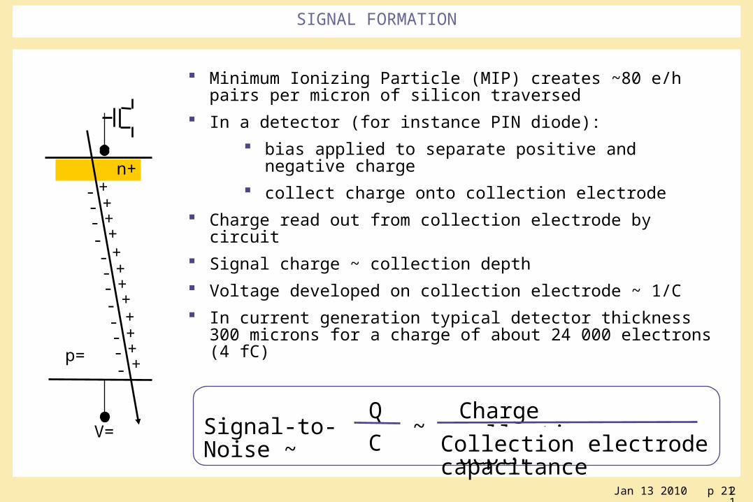
SIGNAL FORMATION
++++
----
Minimum Ionizing Particle (MIP) creates ~80 e/h pairs per micron of silicon traversed
In a detector (for instance PIN diode):
bias applied to separate positive and negative charge
collect charge onto collection electrode
Charge read out from collection electrode by circuit
Signal charge ~ collection depth
Voltage developed on collection electrode ~ 1/C
In current generation typical detector thickness 300 microns for a charge of about 24 000 electrons (4 fC)
++++
----
+++
----
+
n+
p=
V= Signal-to-Noise ~
Charge collection depth~
Collection electrode capacitance
Q
C

Walter Snoeys – CERN – PH – ESE – ME-2009 22
Click to edit the outline text format
Second Outline Level Third Outline Level
Fourth Outline Level Fifth Outline Level Sixth Outline Level Seventh Outline
Level Eighth Outline
Level Ninth Outline LevelClick to edit
Master text styles Second level
Third level Fourth level
Fifth level
Click to edit the outline text format
Second Outline Level Third Outline Level
Fourth Outline Level Fifth Outline Level Sixth Outline Level Seventh Outline
Level Eighth Outline
Level Ninth Outline LevelClick to edit
Master text styles Second level
Third level Fourth level
Fifth level
Click to edit the outline text format
Second Outline Level Third Outline Level
Fourth Outline Level Fifth Outline Level Sixth Outline Level Seventh Outline
Level Eighth Outline
Level Ninth Outline LevelClick to edit
Master text styles Second level
Third level Fourth level
Fifth level
++++
----
++++
----
+++
----
+
n+
p=
V=
MOTIVATION FOR MONOLITHIC DETECTORS
Detector-readout connection automatically realized Cost
one chip instead of two or readout immediately included some monolithic detectors offer lower cost per unit area than
traditional high resistivity silicon detectors alone Less material Low capacitance of the collection electrode allows very
favorable power – signal-to-noise ratios
Signal-to-Noise ~
Charge collection depth~
Collection electrode capacitance
Q
C
Walter Snoeys – CERN – PH – ESE – ME-2009 23
Click to edit Master subtitle style
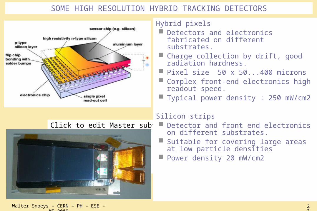
SOME HIGH RESOLUTION HYBRID TRACKING DETECTORS
Hybrid pixels Detectors and electronics fabricated on
different substrates. Charge collection by drift, good radiation
hardness. Pixel size 50 x 50...400 microns Complex front-end electronics high readout
speed. Typical power density : 250 mW/cm2
Silicon strips Detector and front end electronics on different
substrates. Suitable for covering large areas at low particle
densities Power density 20 mW/cm2
Jan 13 2010 p 2424
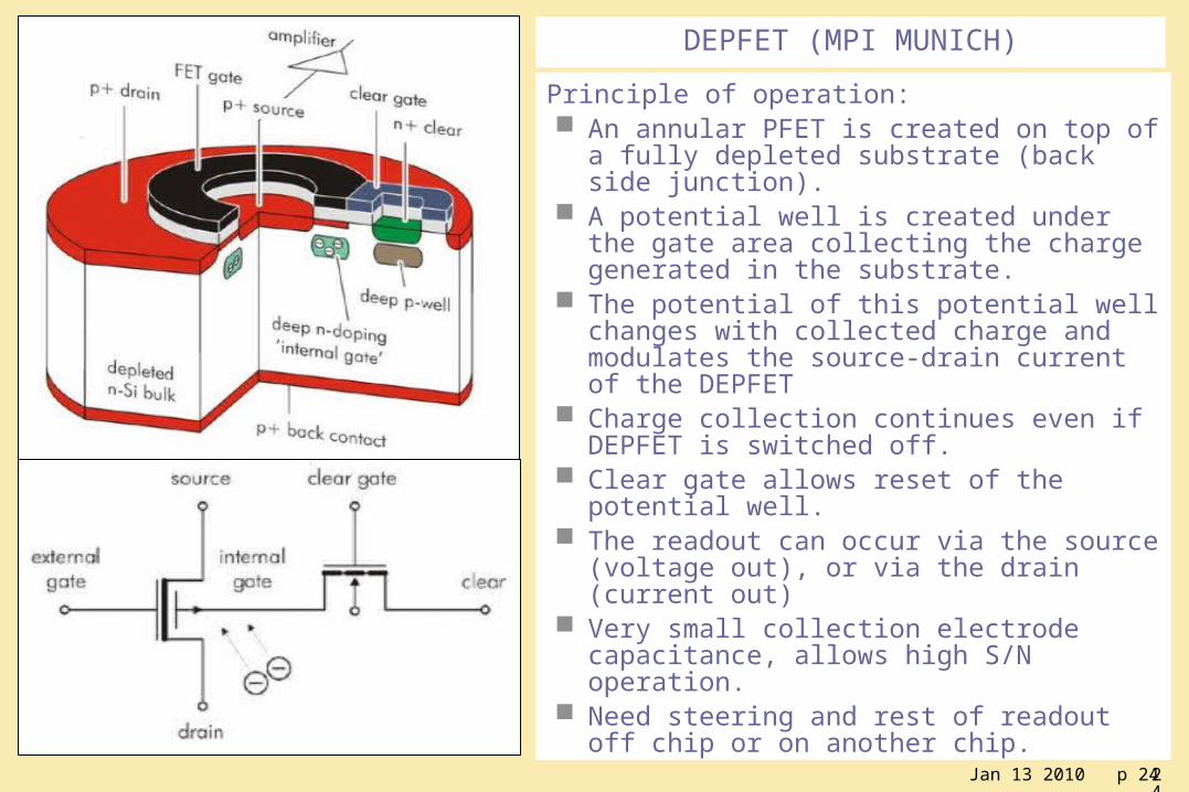
DEPFET (MPI MUNICH)
Principle of operation: An annular PFET is created on top of a fully
depleted substrate (back side junction). A potential well is created under the gate area
collecting the charge generated in the substrate. The potential of this potential well changes with
collected charge and modulates the source-drain current of the DEPFET
Charge collection continues even if DEPFET is switched off.
Clear gate allows reset of the potential well. The readout can occur via the source (voltage
out), or via the drain (current out) Very small collection electrode capacitance,
allows high S/N operation. Need steering and rest of readout off chip or on
another chip.
Jan 13 2010 p 2525
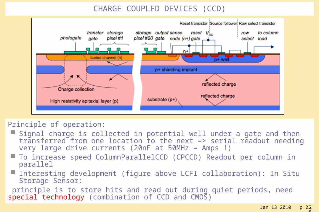
CHARGE COUPLED DEVICES (CCD)
Principle of operation: Signal charge is collected in potential well under a gate and then transferred from one
location to the next => serial readout needing very large drive currents (20nF at 50MHz = Amps !)
To increase speed ColumnParallelCCD (CPCCD) Readout per column in parallel Interesting development (figure above LCFI collaboration): In Situ Storage Sensor:
principle is to store hits and read out during quiet periods, need special technology (combination of CCD and CMOS)
Jan 13 2010 p 2626
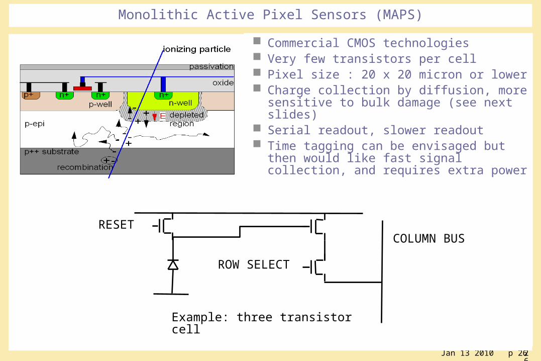
Commercial CMOS technologies Very few transistors per cell Pixel size : 20 x 20 micron or lower Charge collection by diffusion, more sensitive to
bulk damage (see next slides) Serial readout, slower readout Time tagging can be envisaged but then would
like fast signal collection, and requires extra power
Monolithic Active Pixel Sensors (MAPS)
RESETCOLUMN BUS
ROW SELECT
Example: three transistor cell
Jan 13 2010 p 2727
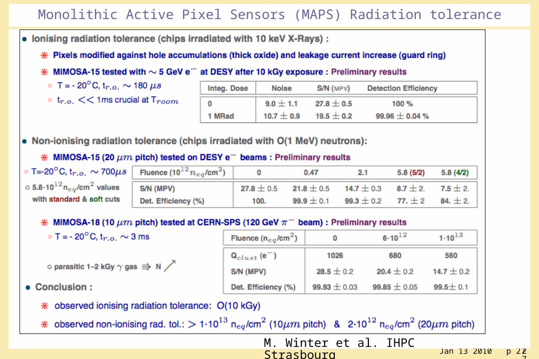
Monolithic Active Pixel Sensors (MAPS) Radiation tolerance
M. Winter et al. IHPC Strasbourg
Jan 13 2010 p 2828
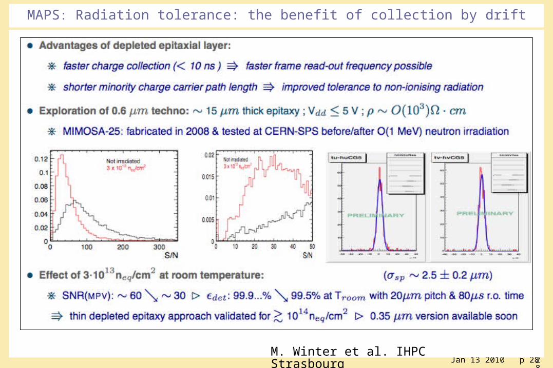
MAPS: Radiation tolerance: the benefit of collection by drift
M. Winter et al. IHPC Strasbourg
Jan 13 2010 p 2929
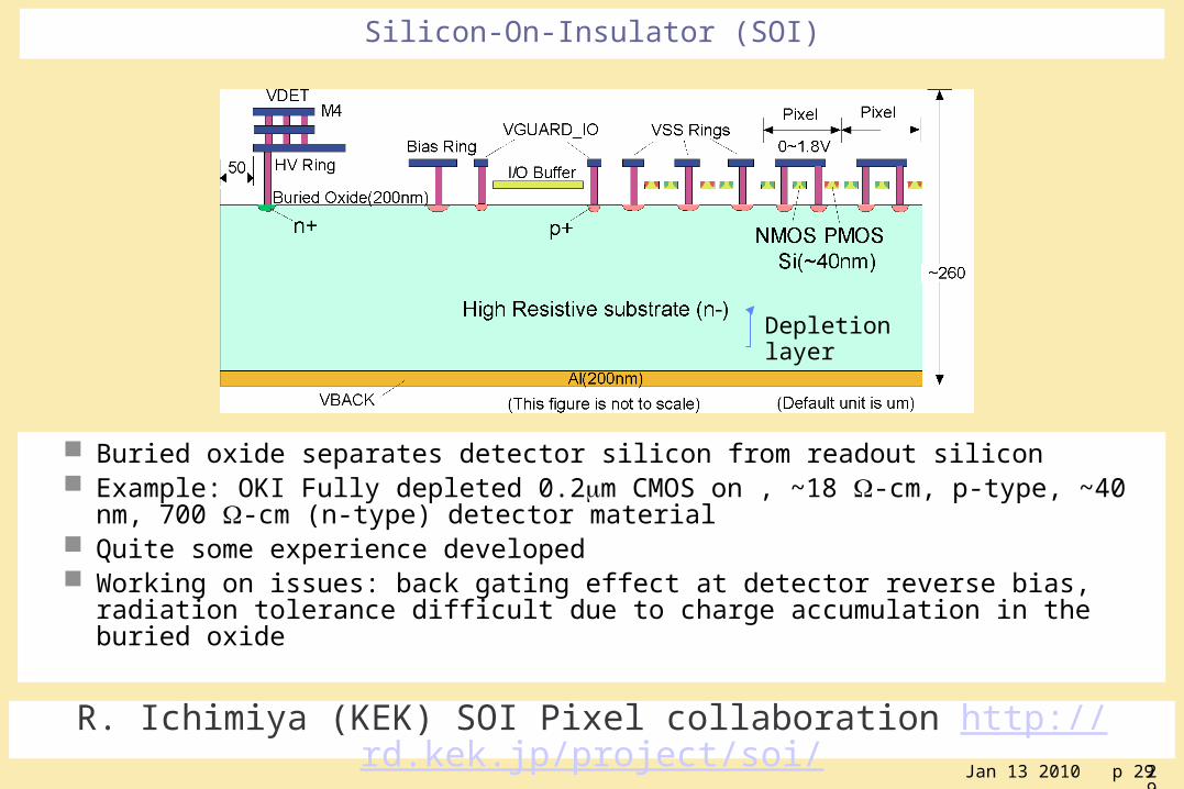
Silicon-On-Insulator (SOI)
R. Ichimiya (KEK) SOI Pixel collaboration http://rd.kek.jp/project/soi/
Buried oxide separates detector silicon from readout silicon Example: OKI Fully depleted 0.2m CMOS on , ~18 -cm, p-type, ~40 nm, 700 -cm (n-
type) detector material Quite some experience developed Working on issues: back gating effect at detector reverse bias, radiation tolerance difficult
due to charge accumulation in the buried oxide
Depletion layer
Jan 13 2010 p 3030
EXAMPLES OF « TRADITIONAL » MONOLITHIC DETECTORS
Non-standard processing on very high resistivity substrate -> volume production is main challenge
CCD on high resistivity substrate DEPFET Stanford-Hawaii …
Or Implementation in more or less standard commercial process
MAPS CCD with epi or on more standard substrate MAPS and CCD based on serial readout Silicon-on-Insulator (SOI) promising but radiation tolerance difficult
Jan 13 2010 p 3131
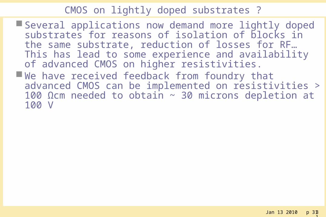
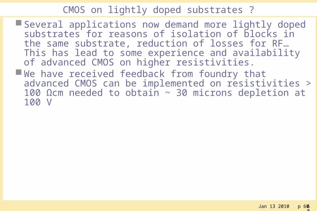
CMOS on lightly doped substrates ?
Several applications now demand more lightly doped substrates for reasons of isolation of blocks in the same substrate, reduction of losses for RF… This has lead to some experience and availability of advanced CMOS on higher resistivities.
We have received feedback from foundry that advanced CMOS can be implemented on resistivities > 100 Ωcm needed to obtain ~ 30 microns depletion at 100 V
Walter Snoeys – CERN – PH – ESE – ME-2009 32
Click to edit Master subtitle style
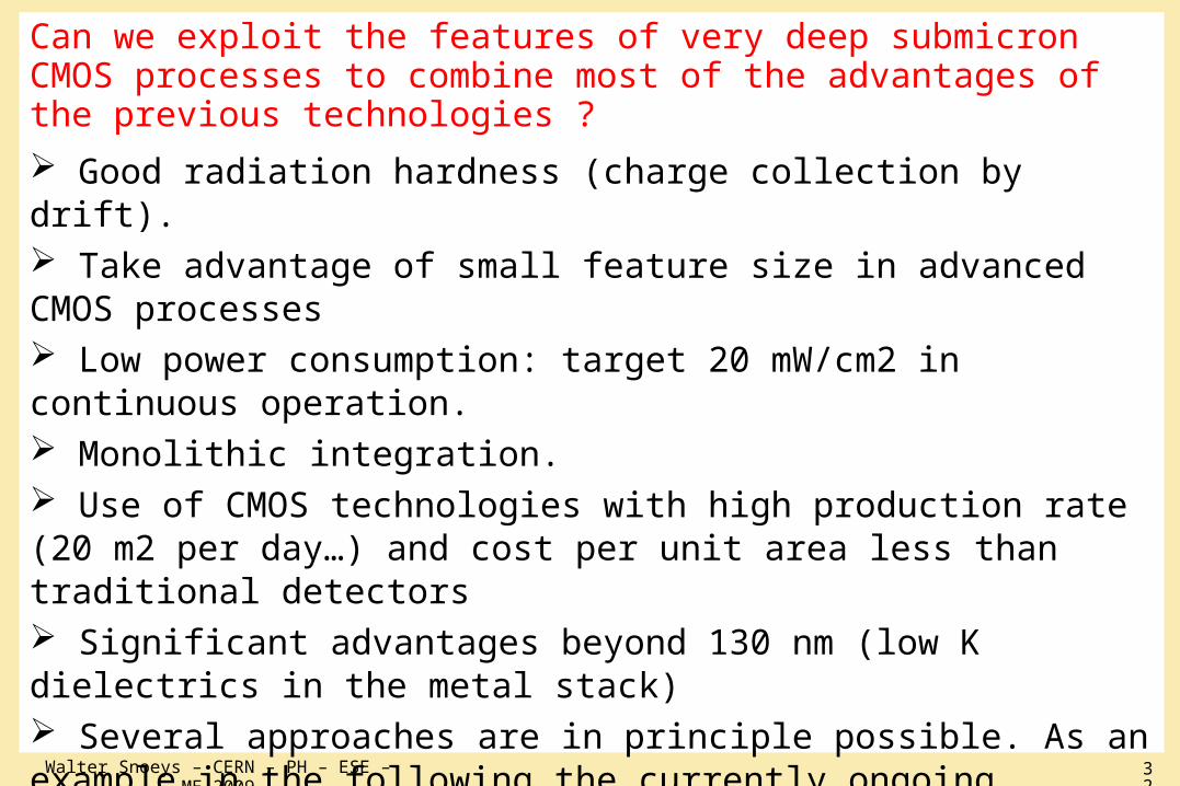
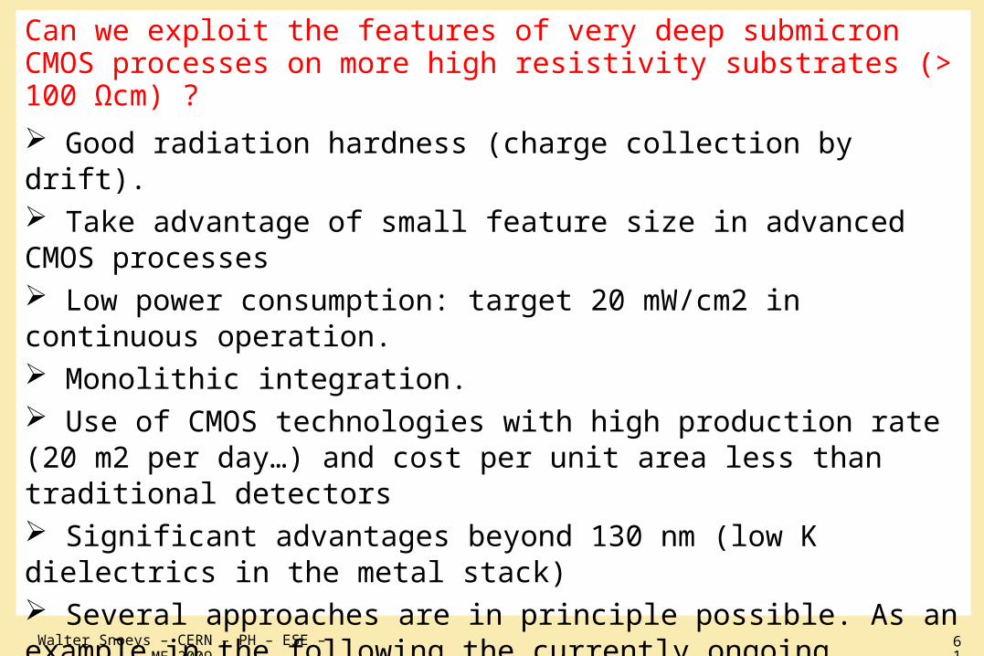
Can we exploit the features of very deep submicron CMOS processes to combine most of the advantages of the previous technologies ?
Good radiation hardness (charge collection by drift). Take advantage of small feature size in advanced CMOS processes Low power consumption: target 20 mW/cm2 in continuous operation. Monolithic integration. Use of CMOS technologies with high production rate (20 m2 per day…) and cost per unit area less than traditional detectors Significant advantages beyond 130 nm (low K dielectrics in the metal stack) Several approaches are in principle possible. As an example in the following the currently ongoing development of LePix will be described. First have a more general look at some issues.
Jan 13 2010 p 3333
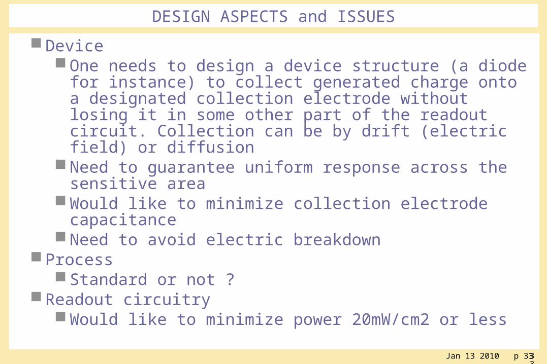
DESIGN ASPECTS and ISSUES
Device One needs to design a device structure (a diode for instance) to
collect generated charge onto a designated collection electrode without losing it in some other part of the readout circuit. Collection can be by drift (electric field) or diffusion
Need to guarantee uniform response across the sensitive area Would like to minimize collection electrode capacitance Need to avoid electric breakdown
Process Standard or not ?
Readout circuitry Would like to minimize power 20mW/cm2 or less
Jan 13 2010 p 3434
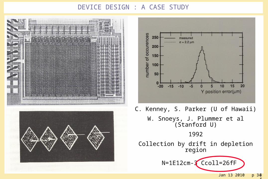
C. Kenney, S. Parker (U of Hawaii)
W. Snoeys, J. Plummer et al (Stanford U)
1992
Collection by drift in depletion region
DEVICE DESIGN : A CASE STUDY
N=1E12cm-3 Ccoll=26fF
Jan 13 2010 p 3535
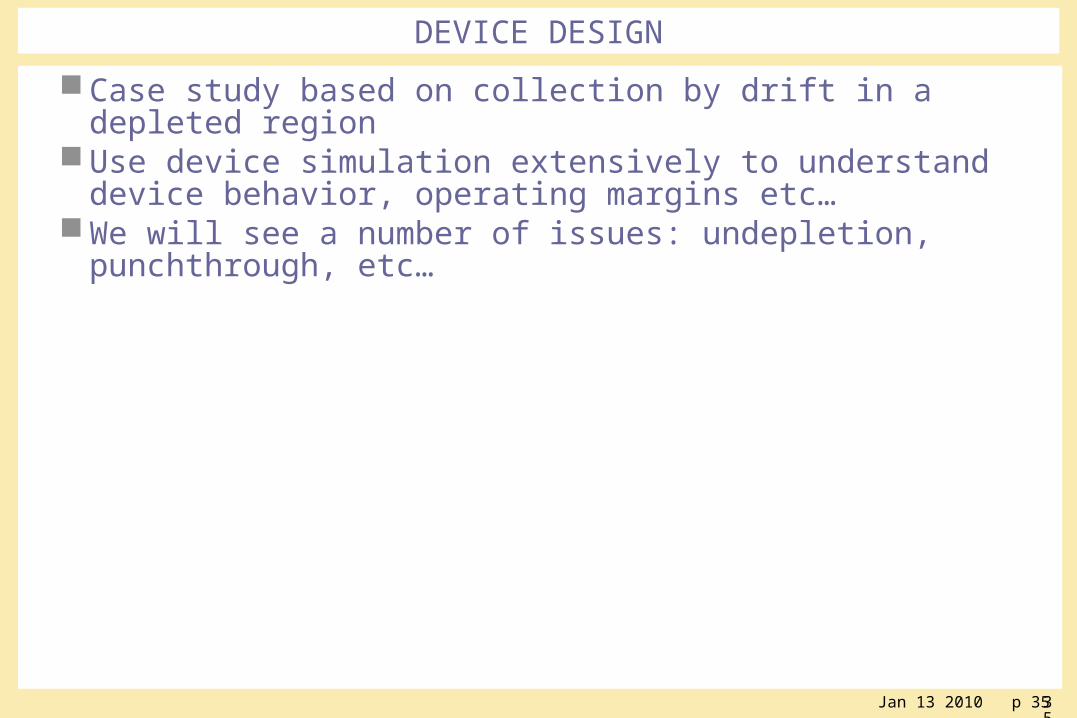
DEVICE DESIGN
Case study based on collection by drift in a depleted region Use device simulation extensively to understand device behavior,
operating margins etc… We will see a number of issues: undepletion, punchthrough, etc…
Jan 13 2010 p 3636
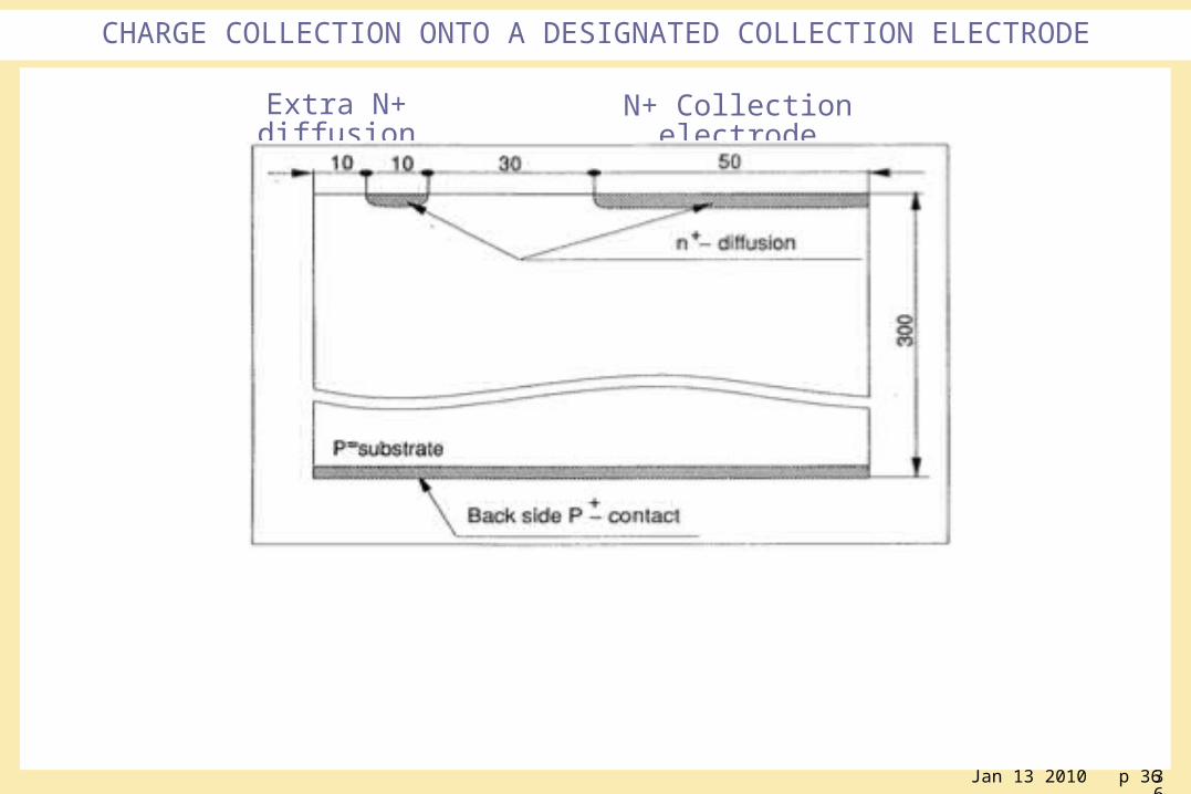
CHARGE COLLECTION ONTO A DESIGNATED COLLECTION ELECTRODE
Extra N+ diffusion N+ Collection electrode
P– substrate N=1012 cm-3
Jan 13 2010 p 3737
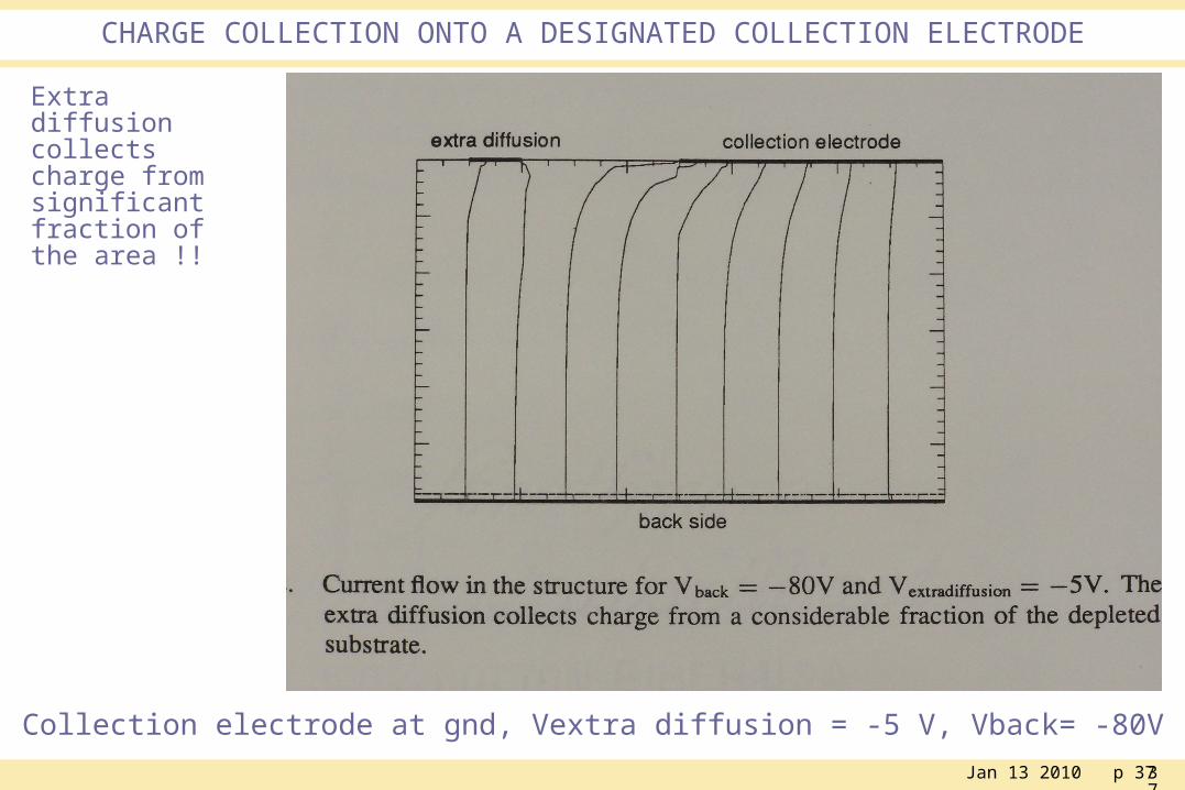
CHARGE COLLECTION ONTO A DESIGNATED COLLECTION ELECTRODE
Collection electrode at gnd, Vextra diffusion = -5 V, Vback= -80V
Extra diffusion collects charge from significant fraction of the area !!
Jan 13 2010 p 3838
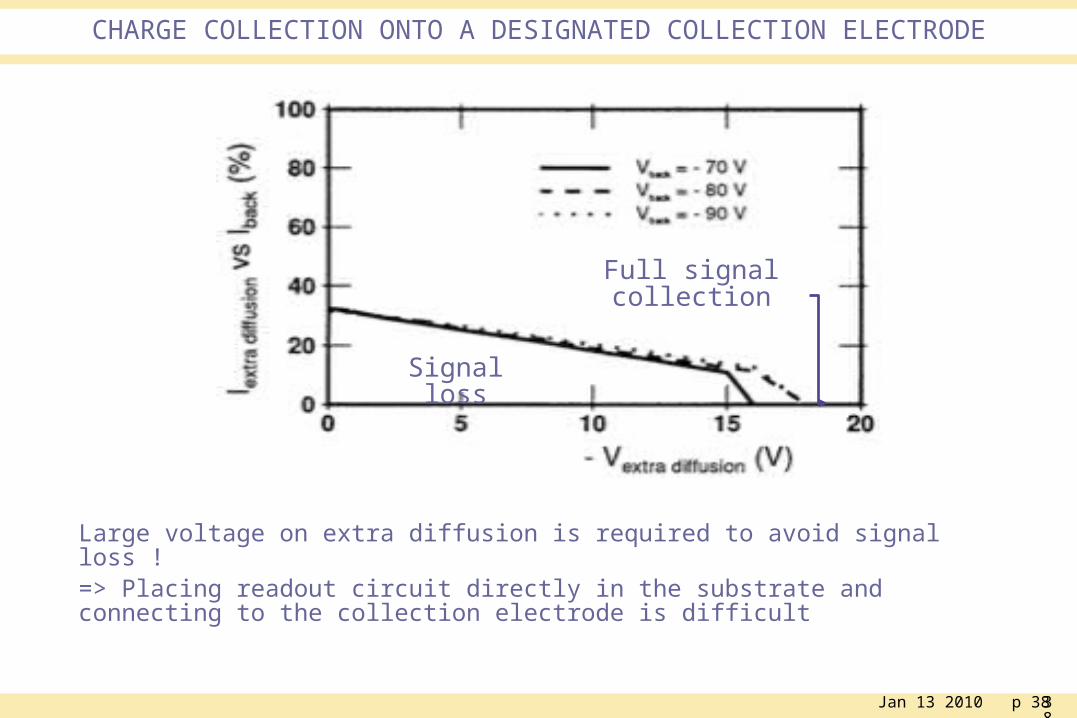
CHARGE COLLECTION ONTO A DESIGNATED COLLECTION ELECTRODE
Large voltage on extra diffusion is required to avoid signal loss !=> Placing readout circuit directly in the substrate and connecting to the collection electrode is difficult
Signal loss
Full signal collection
Jan 13 2010 p 3939
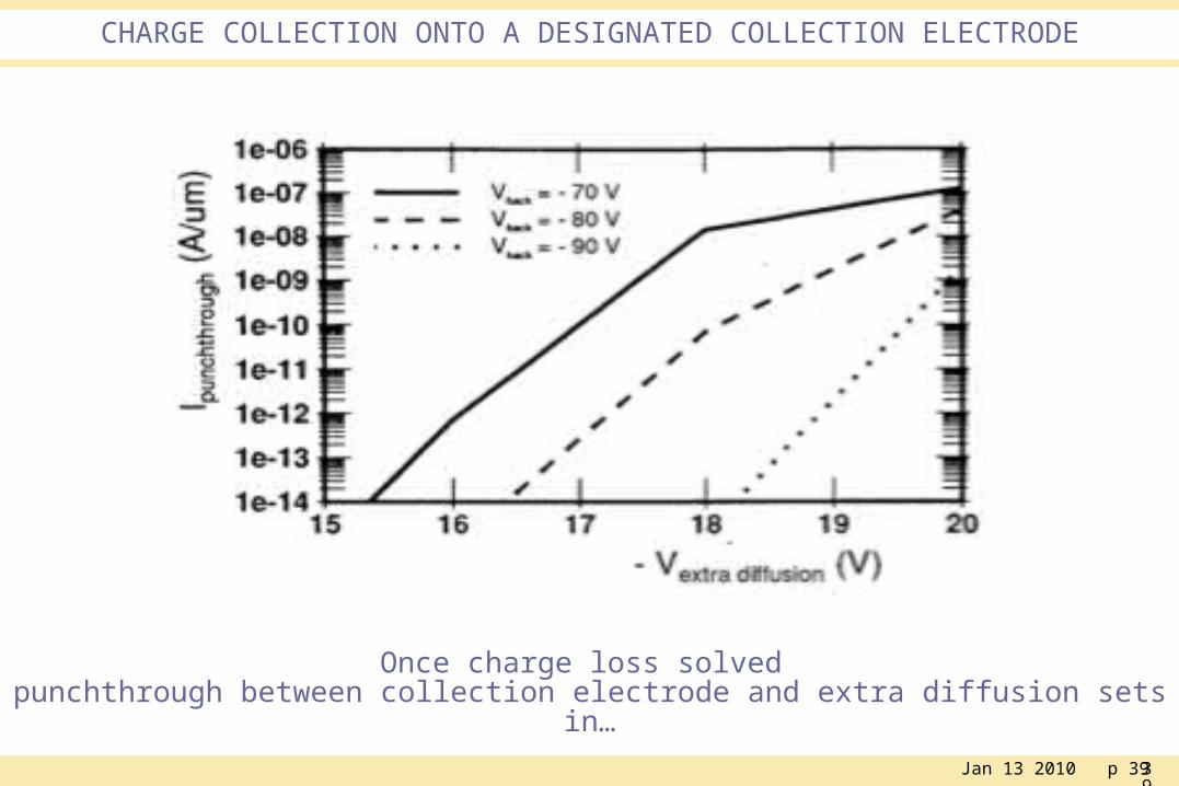
CHARGE COLLECTION ONTO A DESIGNATED COLLECTION ELECTRODE
Once charge loss solved punchthrough between collection electrode and extra diffusion sets in…
Signal loss
Jan 13 2010 p 4040
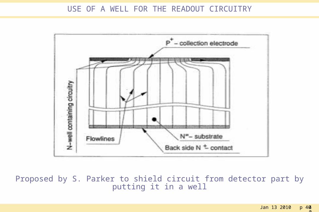
USE OF A WELL FOR THE READOUT CIRCUITRY
Proposed by S. Parker to shield circuit from detector part by putting it in a well
Jan 13 2010 p 4141
USE OF A WELL FOR THE READOUT CIRCUITRY
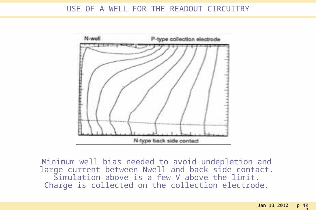
Minimum well bias needed to avoid undepletion and large current between Nwell and back side contact.
Simulation above is a few V above the limit.Charge is collected on the collection electrode.
Jan 13 2010 p 4242
USE OF A WELL FOR THE READOUT CIRCUITRY
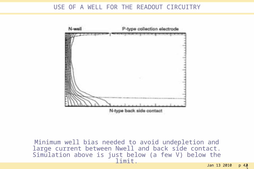
Minimum well bias needed to avoid undepletion and large current between Nwell and back side contact.
Simulation above is just below (a few V) below the limit.
Jan 13 2010 p 4343
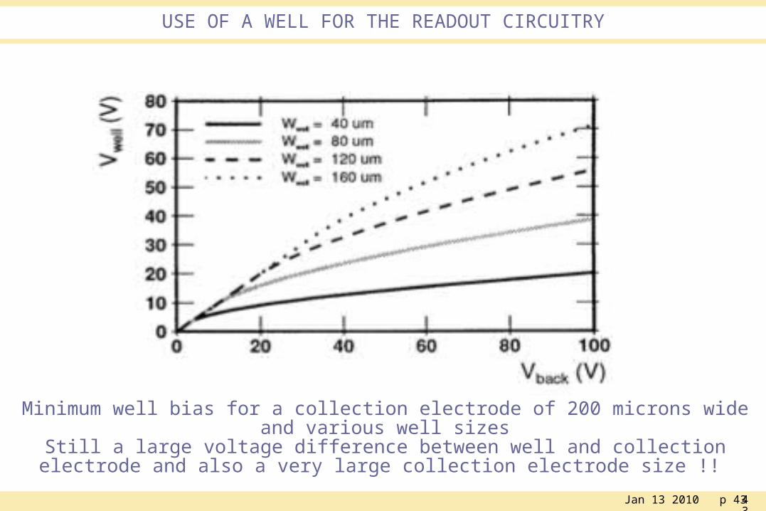
USE OF A WELL FOR THE READOUT CIRCUITRY
Minimum well bias for a collection electrode of 200 microns wide and various well sizesStill a large voltage difference between well and collection electrode and also a very
large collection electrode size !!
Jan 13 2010 p 4444
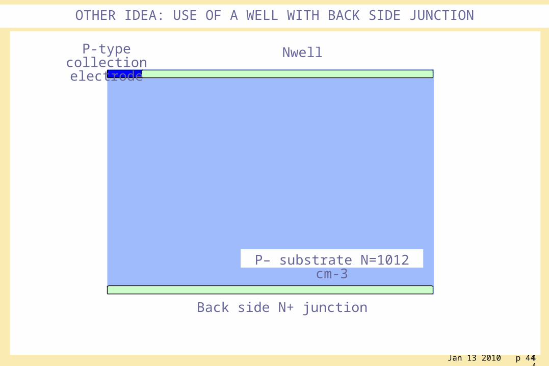
OTHER IDEA: USE OF A WELL WITH BACK SIDE JUNCTION
P-type collection electrode
Nwell
Back side N+ junction
P– substrate N=1012 cm-3
Jan 13 2010 p 4545
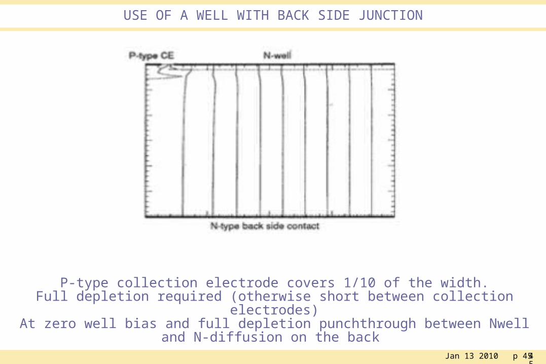
USE OF A WELL WITH BACK SIDE JUNCTION
P-type collection electrode covers 1/10 of the width.Full depletion required (otherwise short between collection electrodes)
At zero well bias and full depletion punchthrough between Nwell and N-diffusion on the back
Jan 13 2010 p 4646
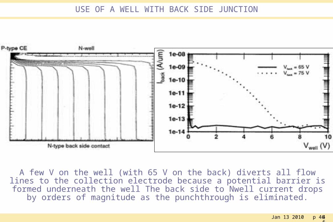
USE OF A WELL WITH BACK SIDE JUNCTION
A few V on the well (with 65 V on the back) diverts all flow lines to the collection electrode because a potential barrier is formed underneath the well The back side to
Nwell current drops by orders of magnitude as the punchthrough is eliminated.
Jan 13 2010 p 4747
USE OF A WELL WITH BACK SIDE JUNCTION
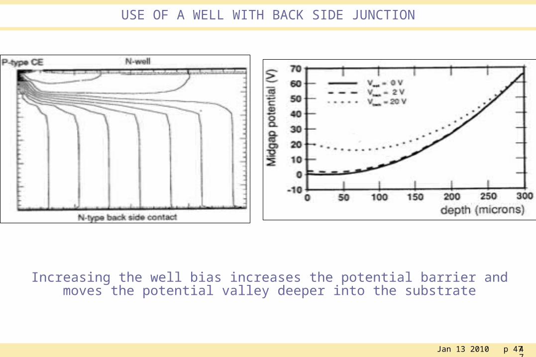
Increasing the well bias increases the potential barrier and moves the potential valley deeper into the substrate
Jan 13 2010 p 4848
USE OF A WELL WITH BACK SIDE JUNCTION
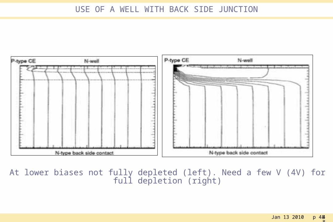
At lower biases not fully depleted (left). Need a few V (4V) for full depletion (right)
Jan 13 2010 p 4949
USE OF A WELL WITH BACK SIDE JUNCTION
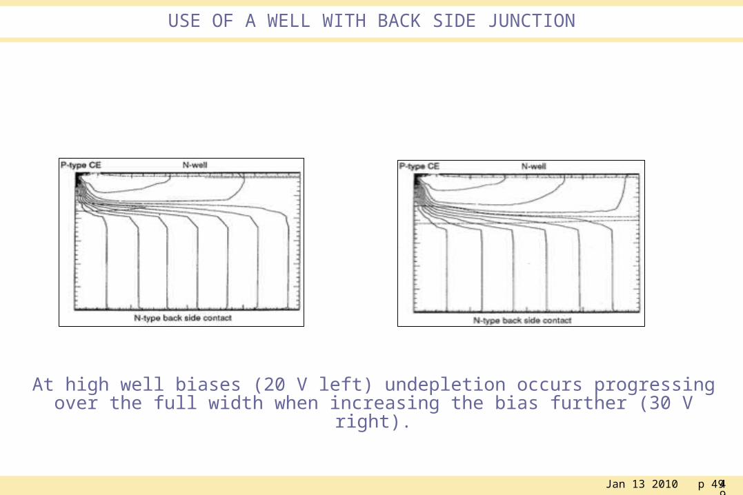
At high well biases (20 V left) undepletion occurs progressing over the full width when increasing the bias further (30 V right).
Jan 13 2010 p 5050
USE OF A WELL WITH BACK SIDE JUNCTION
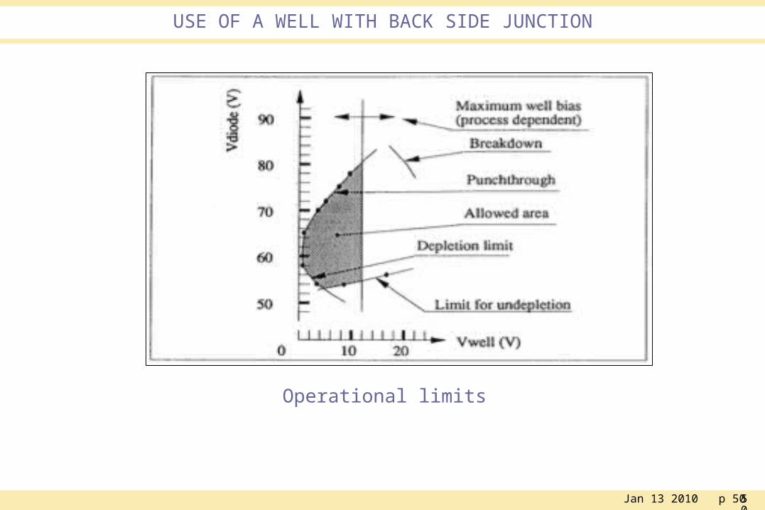
Operational limits
Jan 13 2010 p 5151
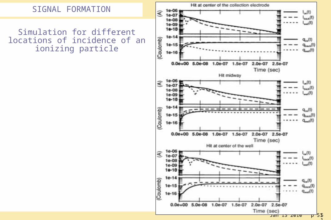
SIGNAL FORMATION
Simulation for different locations of incidence of an ionizing particle
Jan 13 2010 p 5252
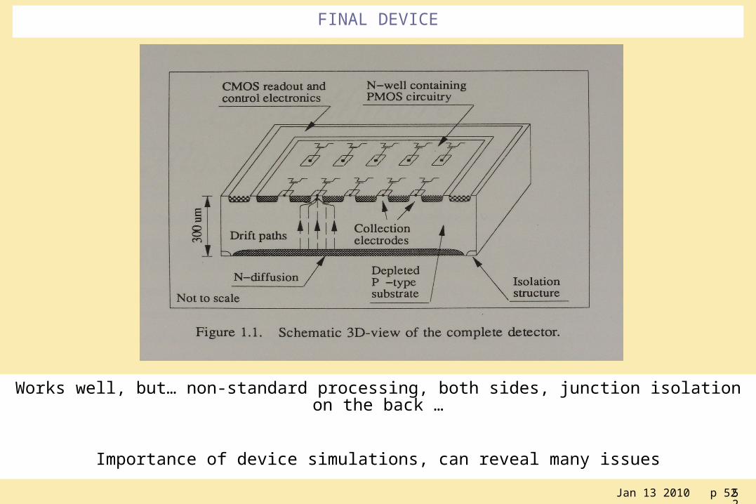
FINAL DEVICE
Works well, but… non-standard processing, both sides, junction isolation on the back …
Importance of device simulations, can reveal many issues
Jan 13 2010 p 5353
PROCESSING just a few remarks
CMOS standard processing quite advanced now on 200 or 300 mm diameter wafers
Processing very high resistivity silicon has some particularities: High resistivity (detector grade) not easily found at larger diameter Float-zone silicon contains much less impurities/defects than
Czochralski. These defects pin down dislocations, rendering the material more robust. Float-zone material is MUCH MORE FRAGILE
Several process steps can introduce impurities which increase detector leakage Can work at higher leakage current (might soon be dominated by
radiation induced leakage) Can try to make certain steps cleaner Can use gettering techniques, which during processing render
defects more mobile and provide traps for these where they are no longer harmful.
Jan 13 2010 p 5454
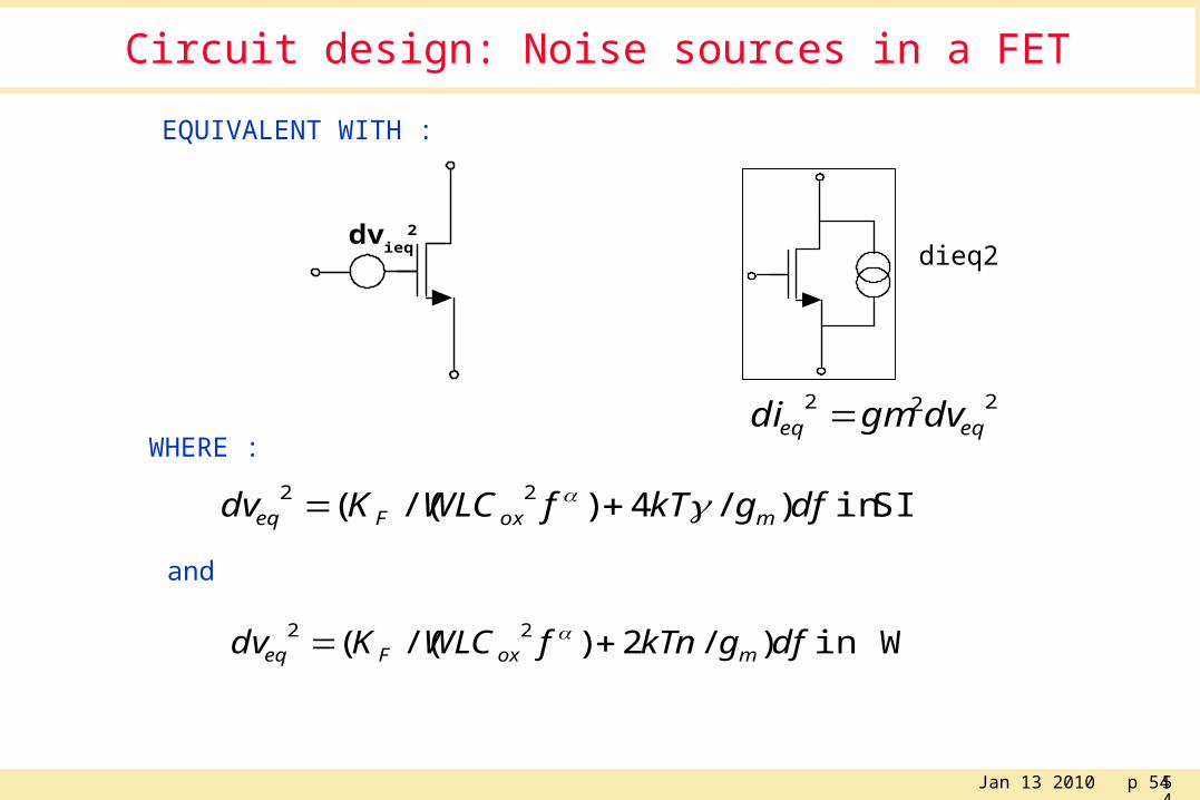
Circuit design: Noise sources in a FET
EQUIVALENT WITH :
WHERE :
dvieq
2
SIin )/4)/(( 22 dfgkTfWLCKdv moxFeq
and
in WI )/2)/(( 22 dfgkTnfWLCKdv moxFeq
222eqeq dvgmdi
dieq2
Jan 13 2010 p 5555
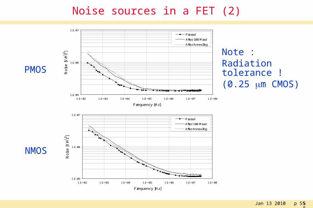
Noise sources in a FET (2)
1.E-09
1.E-08
1.E-07
1.E+02 1.E+03 1.E+04 1.E+05 1.E+06 1.E+07 1.E+08
Frequency [Hz]
Nois
e [V
/Hz1/2]
Prerad
After 100 Mrad
After Annealing
1.E-09
1.E-08
1.E-07
1.E+02 1.E+03 1.E+04 1.E+05 1.E+06 1.E+07 1.E+08
Frequency [Hz]
No
ise
[V
/Hz1/2]
Prerad
After 100 Mrad
After Annealing
NMOS
PMOS
Note :Radiation tolerance !(0.25 m CMOS)
Jan 13 2010 p 5656
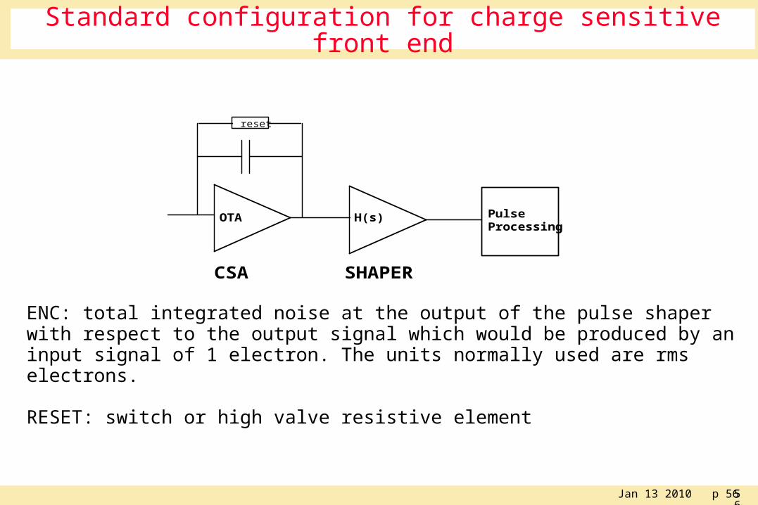
Standard configuration for charge sensitive front end
ENC: total integrated noise at the output of the pulse shaper with respect to the output signal which would be produced by an input signal of 1 electron. The units normally used are rms electrons.
RESET: switch or high valve resistive element
reset
H(s) Pulse Processing
CSA SHAPER
OTA
Jan 13 2010 p 5757
Standard configuration for charge sensitive front end
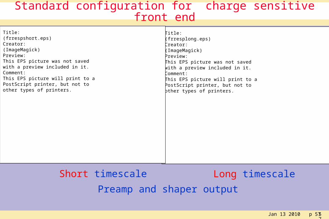
Preamp and shaper output
Short timescale Long timescale
Title:(frresplong.eps)Creator:(ImageMagick)Preview:This EPS picture was not savedwith a preview included in it.Comment:This EPS picture will print to aPostScript printer, but not toother types of printers.
Title:(frrespshort.eps)Creator:(ImageMagick)Preview:This EPS picture was not savedwith a preview included in it.Comment:This EPS picture will print to aPostScript printer, but not toother types of printers.
Jan 13 2010 p 5858
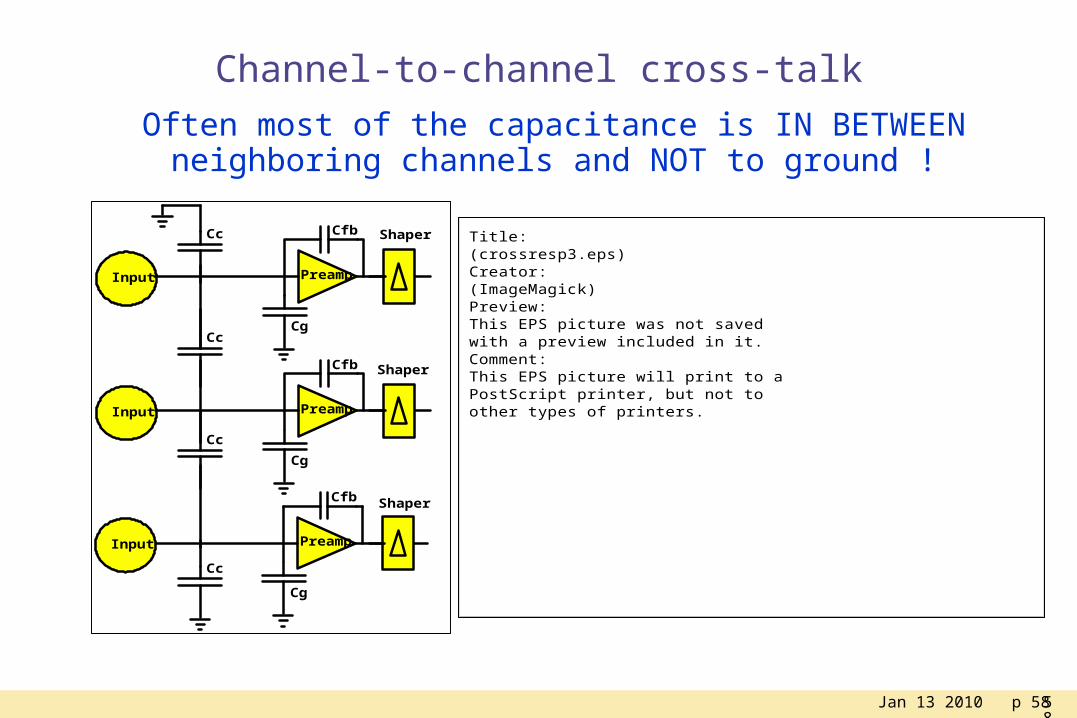
Channel-to-channel cross-talk
Often most of the capacitance is IN BETWEEN neighboring channels and NOT to ground !
Title:(crossresp3.eps)Creator:(ImageMagick)Preview:This EPS picture was not savedwith a preview included in it.Comment:This EPS picture will print to aPostScript printer, but not toother types of printers.
ShaperCfb
Input Preamp
CgCc
Cfb
Input Preamp
Cg
Cfb
Input Preamp
Cg
Cc
Cc
Cc
Shaper
Shaper
Jan 13 2010 p 5959
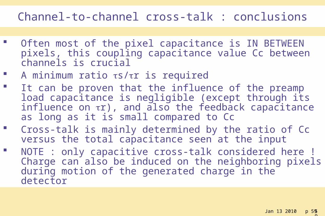
Channel-to-channel cross-talk : conclusions
Often most of the pixel capacitance is IN BETWEEN pixels, this coupling capacitance value Cc between channels is crucial
A minimum ratio s/r is required It can be proven that the influence of the preamp load capacitance is
negligible (except through its influence on r), and also the feedback capacitance as long as it is small compared to Cc
Cross-talk is mainly determined by the ratio of Cc versus the total capacitance seen at the input
NOTE : only capacitive cross-talk considered here ! Charge can also be induced on the neighboring pixels during motion of the generated charge in the detector
Jan 13 2010 p 6060
CMOS on lightly doped substrates ?
Several applications now demand more lightly doped substrates for reasons of isolation of blocks in the same substrate, reduction of losses for RF… This has lead to some experience and availability of advanced CMOS on higher resistivities.
We have received feedback from foundry that advanced CMOS can be implemented on resistivities > 100 Ωcm needed to obtain ~ 30 microns depletion at 100 V
Walter Snoeys – CERN – PH – ESE – ME-2009 61
Click to edit Master subtitle style
Can we exploit the features of very deep submicron CMOS processes on more high resistivity substrates (> 100 Ωcm) ?
Good radiation hardness (charge collection by drift). Take advantage of small feature size in advanced CMOS processes Low power consumption: target 20 mW/cm2 in continuous operation. Monolithic integration. Use of CMOS technologies with high production rate (20 m2 per day…) and cost per unit area less than traditional detectors Significant advantages beyond 130 nm (low K dielectrics in the metal stack) Several approaches are in principle possible. As an example in the following the currently ongoing development of LePIX will be described.
Walter Snoeys – CERN – PH – ESE – ME-2009 62
Click to edit Master subtitle style
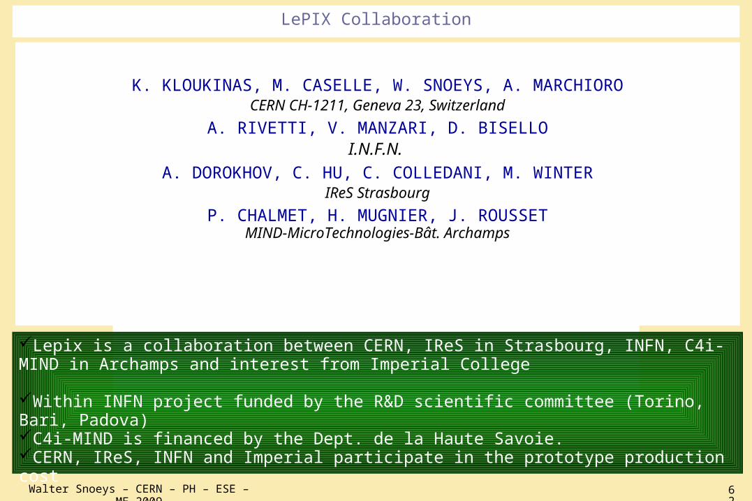
Lepix is a collaboration between CERN, IReS in Strasbourg, INFN, C4i-MIND in Archamps and interest from Imperial College
Within INFN project funded by the R&D scientific committee (Torino, Bari, Padova)C4i-MIND is financed by the Dept. de la Haute Savoie.CERN, IReS, INFN and Imperial participate in the prototype production cost
LePIX Collaboration
K. KLOUKINAS, M. CASELLE, W. SNOEYS, A. MARCHIOROCERN CH-1211, Geneva 23, Switzerland
A. RIVETTI, V. MANZARI, D. BISELLOI.N.F.N.
A. DOROKHOV, C. HU, C. COLLEDANI, M. WINTERIReS Strasbourg
P. CHALMET, H. MUGNIER, J. ROUSSETMIND-MicroTechnologies-Bât. Archamps
Walter Snoeys – CERN – PH – ESE – ME-2009 63
Click to edit the outline text format
Second Outline Level Third Outline Level
Fourth Outline Level Fifth Outline Level Sixth Outline Level Seventh Outline
Level Eighth Outline
Level Ninth Outline LevelClick to edit
Master text styles Second level
Third level Fourth level
Fifth level
Click to edit the outline text format
Second Outline Level Third Outline Level
Fourth Outline Level Fifth Outline Level Sixth Outline Level Seventh Outline
Level Eighth Outline
Level Ninth Outline LevelClick to edit
Master text styles Second level
Third level Fourth level
Fifth level
Click to edit the outline text format
Second Outline Level Third Outline Level
Fourth Outline Level Fifth Outline Level Sixth Outline Level Seventh Outline
Level Eighth Outline
Level Ninth Outline LevelClick to edit
Master text styles Second level
Third level Fourth level
Fifth level
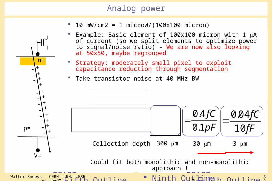
Analog power
++++
----
++++
----
+++
----
+
n+
p=
V=
300 m 30 m 3 m Collection depth
Could fit both monolithic and non-monolithic approach !
fF
fC
10
04.0
pF
fC
1.0
4.0
10 mW/cm2 = 1 microW/(100x100 micron)
Example: Basic element of 100x100 micron with 1 A of current (so we split elements to optimize power to signal/noise ratio) – We are now also looking at 50x50, maybe regrouped
Strategy: moderately small pixel to exploit capacitance reduction through segmentation
Take transistor noise at 40 MHz BW
Jan 13 2010 p 6464
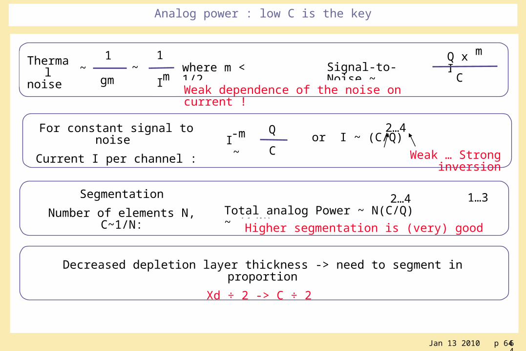
Analog power : low C is the key
Thermal noise
1
gm
1
I mwhere m < 1/2~ Signal-to-Noise ~
Q x I
C
m
Weak dependence of the noise on current !
I ~ For constant signal to noise
Current I per channel :
Q
C
-m or I ~ (C/Q) 2…4
Segmentation
Number of elements N, C~1/N: Total analog Power ~ N(C/Q) ~ (1/N) 1…32…4
Higher segmentation is (very) good
Decreased depletion layer thickness -> need to segment in proportion
Xd ÷ 2 -> C ÷ 2
Weak … Strong inversion
~
Jan 13 2010 p 6565
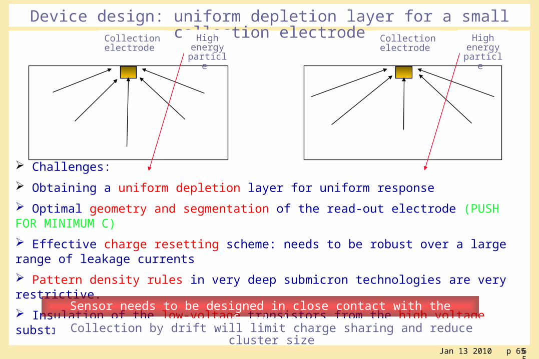
Device design: uniform depletion layer for a small collection electrodeCollection electrode
High energy particle
Collection electrode
High energy particle
Challenges:
Obtaining a uniform depletion layer for uniform response
Optimal geometry and segmentation of the read-out electrode (PUSH FOR MINIMUM C)
Effective charge resetting scheme: needs to be robust over a large range of leakage currents
Pattern density rules in very deep submicron technologies are very restrictive.
Insulation of the low-voltage transistors from the high voltage substrate.
Sensor needs to be designed in close contact with the foundry!
Collection by drift will limit charge sharing and reduce cluster size
Walter Snoeys – CERN – PH – ESE – ME-2009 66
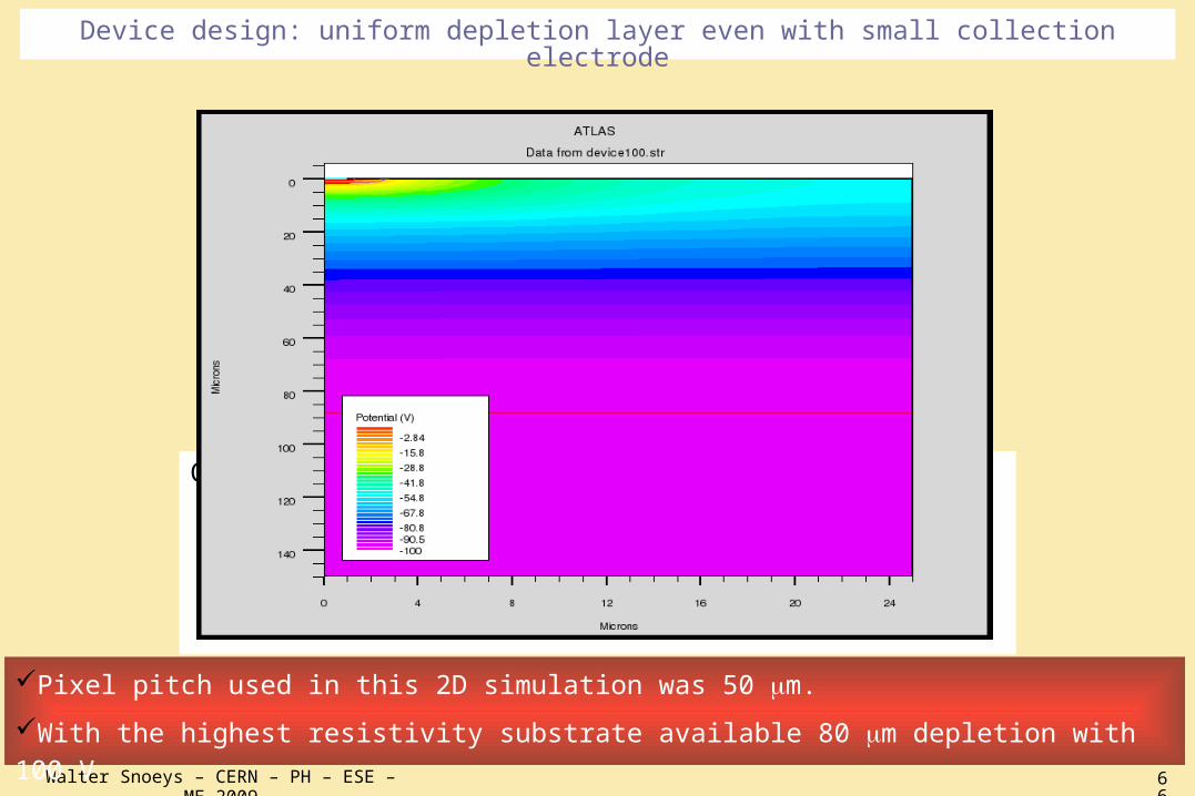
Click to edit Master subtitle style
Pixel pitch used in this 2D simulation was 50 m.
With the highest resistivity substrate available 80 m depletion with 100 V
Device design: uniform depletion layer even with small collection electrode
Jan 13 2010 p 6767
Small collection electrode
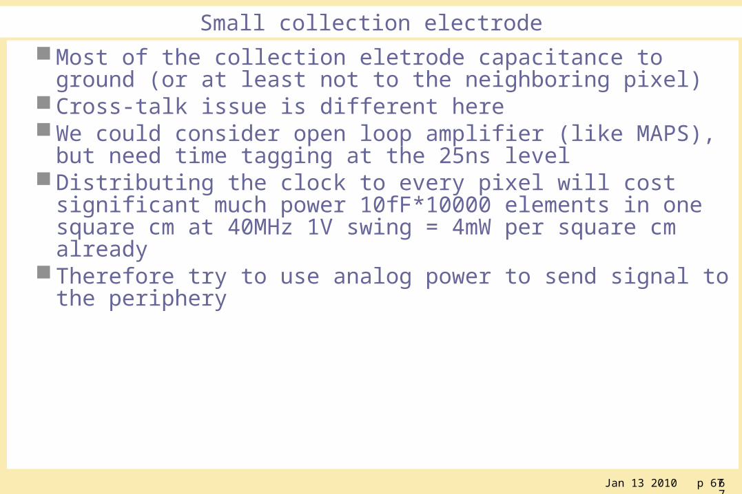
Most of the collection eletrode capacitance to ground (or at least not to the neighboring pixel)
Cross-talk issue is different here We could consider open loop amplifier (like MAPS), but need time
tagging at the 25ns level Distributing the clock to every pixel will cost significant much power
10fF*10000 elements in one square cm at 40MHz 1V swing = 4mW per square cm already
Therefore try to use analog power to send signal to the periphery
Walter Snoeys – CERN – PH – ESE – ME-2009 68
Click to edit Master subtitle style
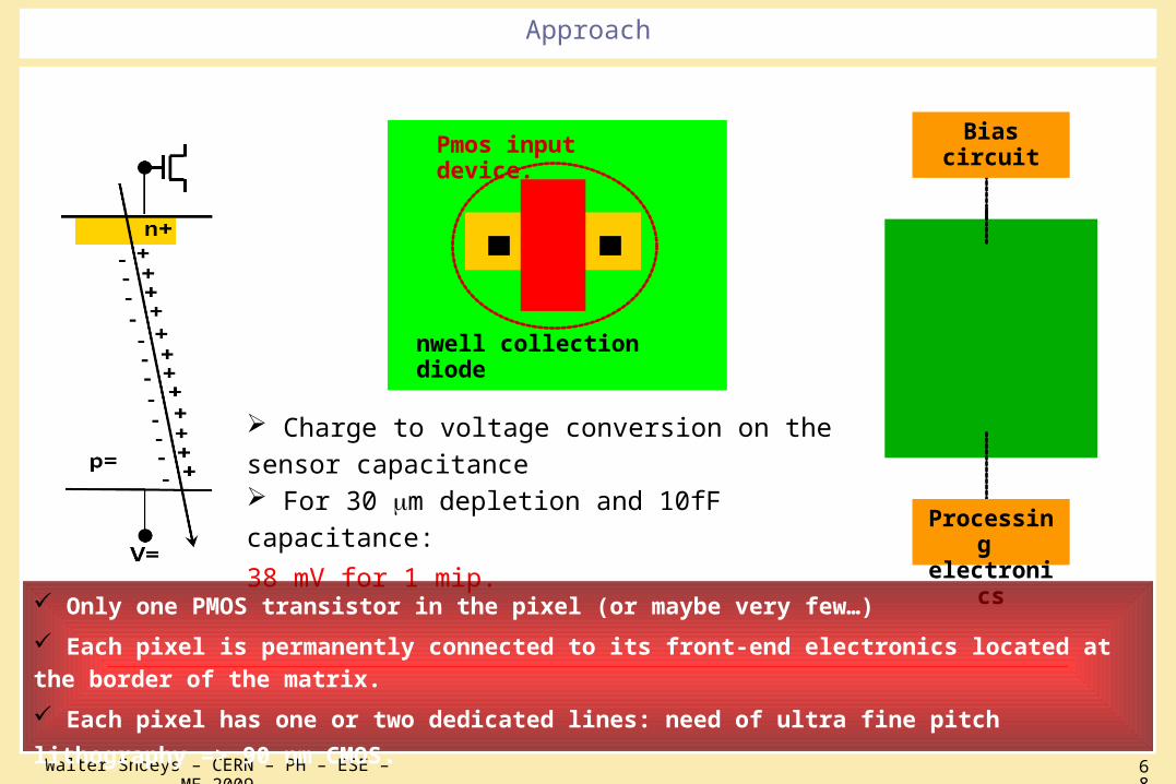
nwell collection diode
Pmos input device.
Charge to voltage conversion on the sensor capacitance For 30 m depletion and 10fF capacitance:
38 mV for 1 mip.
Bias circuit
Processing electronics
Only one PMOS transistor in the pixel (or maybe very few…)
Each pixel is permanently connected to its front-end electronics located at the border of the matrix.
Each pixel has one or two dedicated lines: need of ultra fine pitch lithography =>
90 nm CMOS.
Approach
Walter Snoeys – CERN – PH – ESE – ME-2009 69
Click to edit Master subtitle style
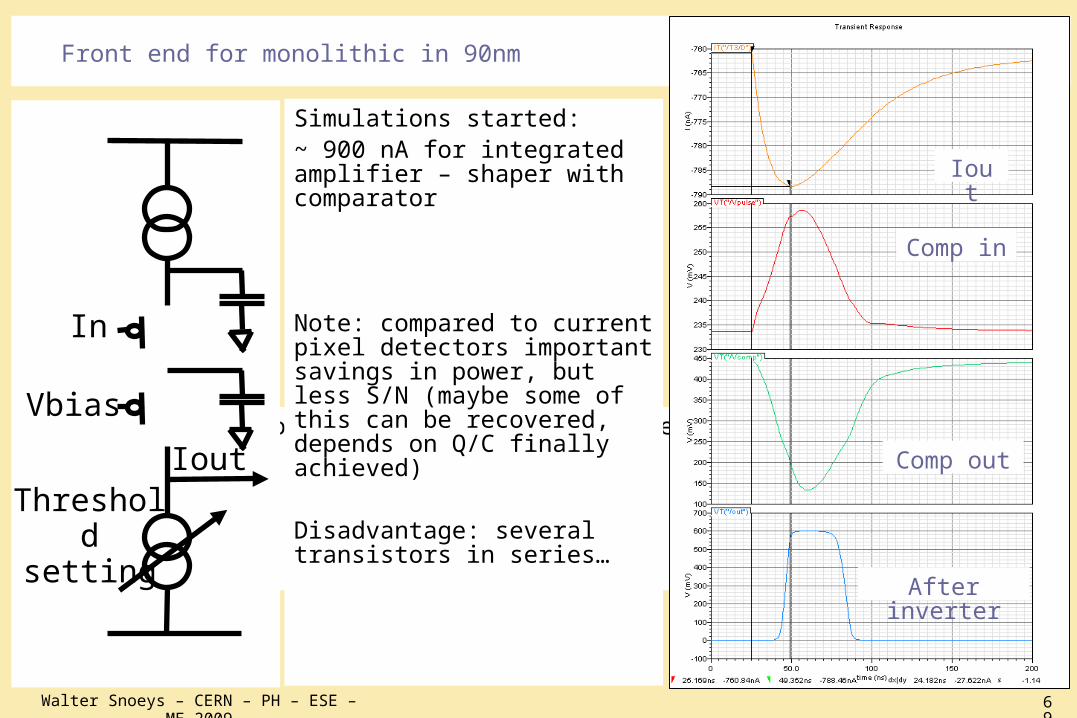
Simulations started:~ 900 nA for integrated amplifier – shaper with comparator
Note: compared to current pixel detectors important savings in power, but less S/N (maybe some of this can be recovered, depends on Q/C finally achieved)
Disadvantage: several transistors in series…
Front end for monolithic in 90nm
Iout
Comp in
Comp out
After inverter
In
Vbias
IoutThreshold
setting
Walter Snoeys – CERN – PH – ESE – ME-2009 70
Click to edit Master subtitle style
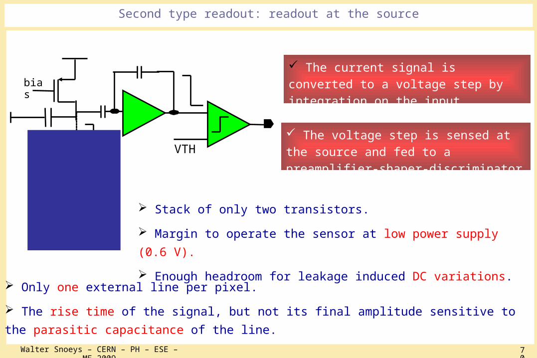
bias
VTH
Only one external line per pixel.
The rise time of the signal, but not its final amplitude sensitive to the parasitic
capacitance of the line.
The current signal is converted to a voltage step by integration on the input parasitic capacitance (~ 10 fF).
The voltage step is sensed at the source and fed to a preamplifier-shaper-discriminator chain .
Stack of only two transistors.
Margin to operate the sensor at low power supply (0.6 V).
Enough headroom for leakage induced DC variations.
Second type readout: readout at the source
Jan 13 2010 p 7171
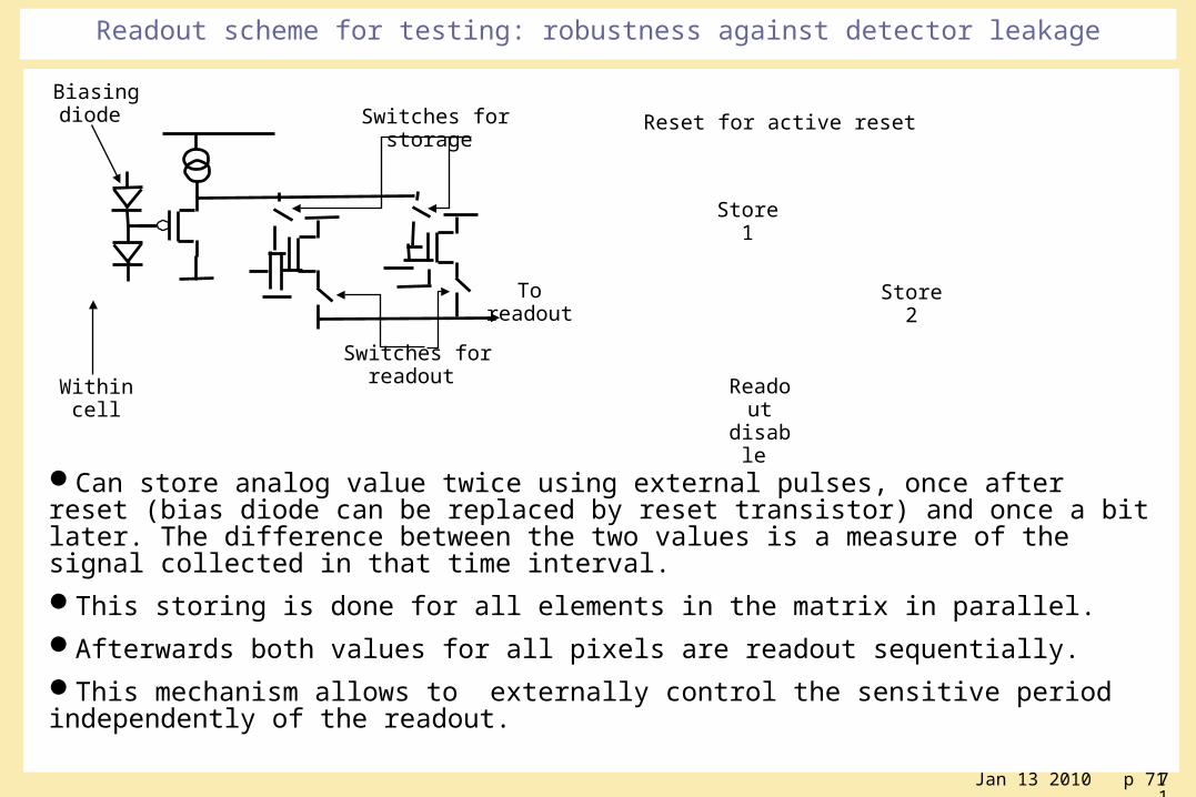
Readout scheme for testing: robustness against detector leakage
Can store analog value twice using external pulses, once after reset (bias diode can be replaced by reset transistor) and once a bit later. The difference between the two values is a measure of the signal collected in that time interval.
This storing is done for all elements in the matrix in parallel.
Afterwards both values for all pixels are readout sequentially.
This mechanism allows to externally control the sensitive period independently of the readout.
Within cell
To readout
Biasing diode Switches for
storage
Switches for readout
Reset for active reset
Store 1
Store 2
Readout
disable
Walter Snoeys – CERN – PH – ESE – ME-2009 72
Matrix of 32x32 pixels – Pixel 50x50µm²
32 Pixels
Analog Amplifier
Digital Part
Pixel 50x50µm²
Digital part
Jan 13 2010 p 7373
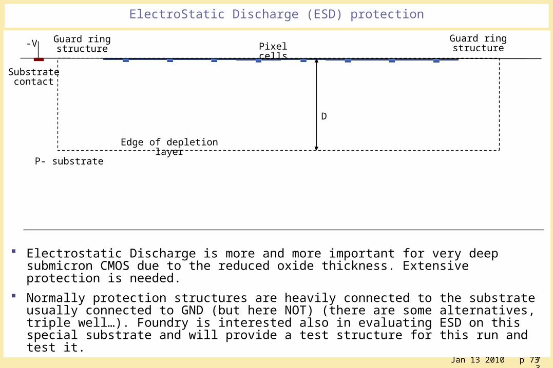
ElectroStatic Discharge (ESD) protection
P- substrate
Edge of depletion layer
-V
D
Guard ring structure
Guard ring structure Pixel cells
Substrate contact
Electrostatic Discharge is more and more important for very deep submicron CMOS due to the reduced oxide thickness. Extensive protection is needed.
Normally protection structures are heavily connected to the substrate usually connected to GND (but here NOT) (there are some alternatives, triple well…). Foundry is interested also in evaluating ESD on this special substrate and will provide a test structure for this run and test it.
Jan 13 2010 p 7474
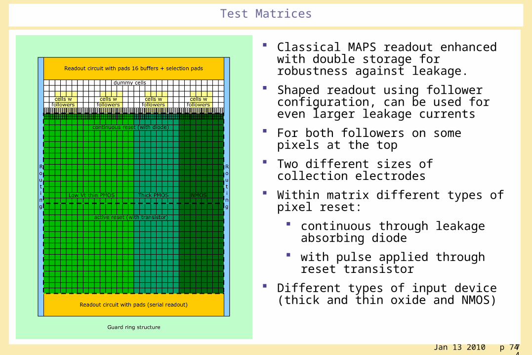
Test Matrices
Classical MAPS readout enhanced with double storage for robustness against leakage.
Shaped readout using follower configuration, can be used for even larger leakage currents
For both followers on some pixels at the top
Two different sizes of collection electrodes
Within matrix different types of pixel reset:
continuous through leakage absorbing diode
with pulse applied through reset transistor
Different types of input device (thick and thin oxide and NMOS)

Jan 13 2010 p 7575
Prototyping status Foundry proposed MPW instead of engineering run for prototyping for cost reduction. We
are in contact with the MPW service and have visited the foundry early September to have another discussion with their technical specialists
Would like to submit a prototype in February (October run was cancelled):
Test structures to characterize the substrate doping, structures allowing resistance measurements, some diodes, etc…
Transistor test structures for model verification, and for irradiation measurements. (First version almost finished, previously submitted to other foundry as well)
ESD test structures
A matrix in a few variants with readout compatible with existing test setups
A matrix in a few variants with a fast shaping front end. Both types of matrices will be equipped with test cells which can receive an electrical test input, and of which some are connected to buffer amplifiers capable of driving the signals off-chip.
Jan 13 2010 p 7676
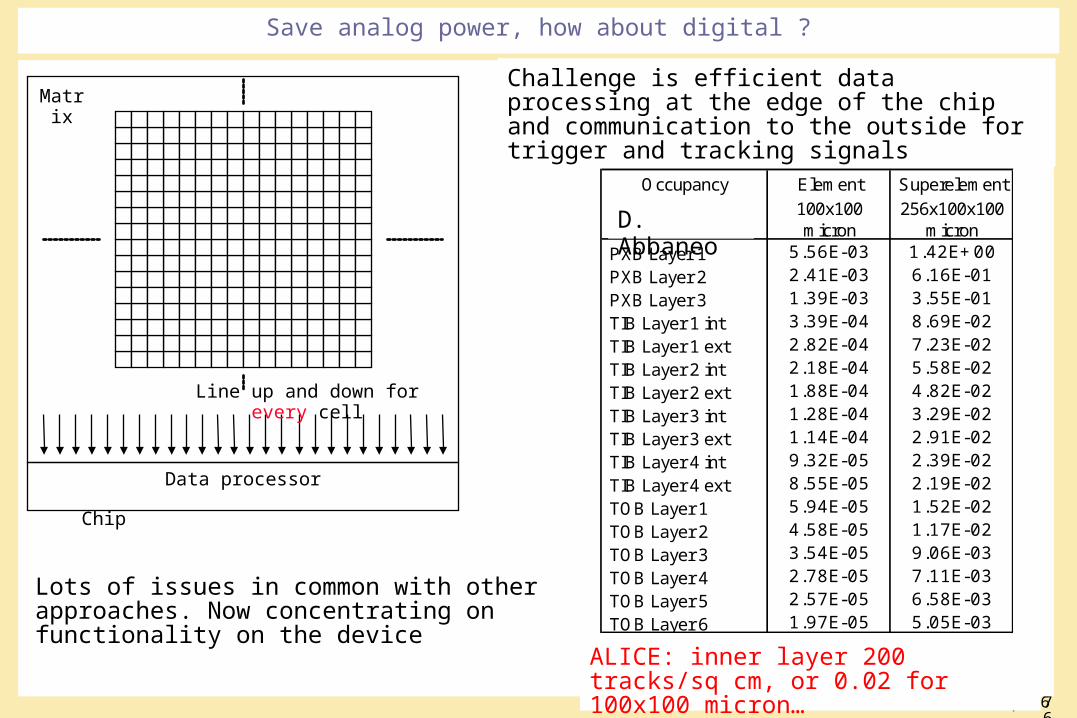
Save analog power, how about digital ?
Challenge is efficient data processing at the edge of the chip and communication to the outside for trigger and tracking signals
Data processor
Chip
Matrix
Line up and down for every cell
Occupancy Element Superelement
100x100 micron
256x100x100micron
PXB Layer 1 5.56E-03 1.42E+00 PXB Layer 2 2.41E-03 6.16E-01 PXB Layer 3 1.39E-03 3.55E-01 TIB Layer 1 int 3.39E-04 8.69E-02 TIB Layer 1 ext 2.82E-04 7.23E-02 TIB Layer 2 int 2.18E-04 5.58E-02 TIB Layer 2 ext 1.88E-04 4.82E-02 TIB Layer 3 int 1.28E-04 3.29E-02 TIB Layer 3 ext 1.14E-04 2.91E-02 TIB Layer 4 int 9.32E-05 2.39E-02 TIB Layer 4 ext 8.55E-05 2.19E-02 TOB Layer 1 5.94E-05 1.52E-02 TOB Layer 2 4.58E-05 1.17E-02 TOB Layer 3 3.54E-05 9.06E-03 TOB Layer 4 2.78E-05 7.11E-03 TOB Layer 5 2.57E-05 6.58E-03 TOB Layer 6 1.97E-05 5.05E-03
D. Abbaneo
Lots of issues in common with other approaches. Now concentrating on functionality on the device
ALICE: inner layer 200 tracks/sq cm, or 0.02 for 100x100 micron…
Jan 13 2010 p 7777
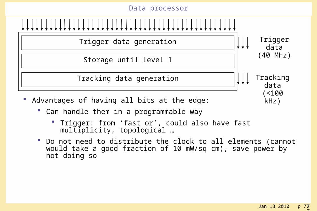
Data processor
Advantages of having all bits at the edge:
Can handle them in a programmable way
Trigger: from ‘fast or’, could also have fast multiplicity, topological …
Do not need to distribute the clock to all elements (cannot would take a good fraction of 10 mW/sq cm), save power by not doing so
Trigger data generation Trigger data(40 MHz)
Storage until level 1
Tracking data generation Tracking data
(<100 kHz)
Jan 13 2010 p 7878
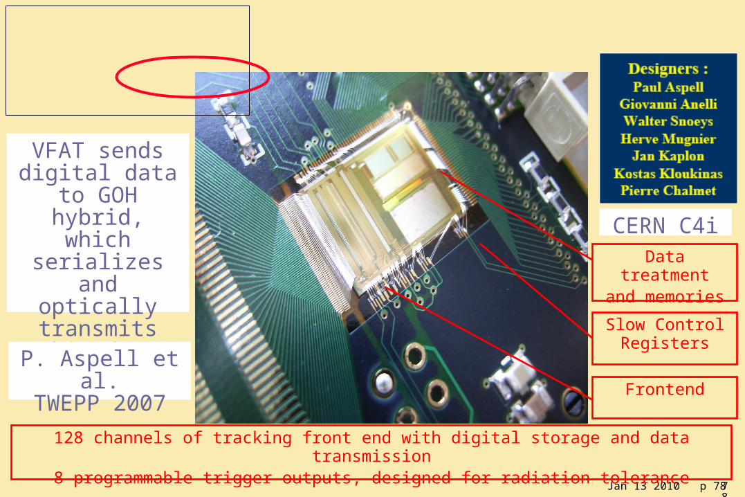
Frontend
Data treatmentand memories
Slow Control Registers
128 channels of tracking front end with digital storage and data transmission8 programmable trigger outputs, designed for radiation tolerance
VFAT sends digital data to GOH hybrid,
which serializes and optically transmits this
data
CERN C4i
P. Aspell et al.TWEPP 2007
Walter Snoeys – CERN – PH – ESE – ME-2009 79
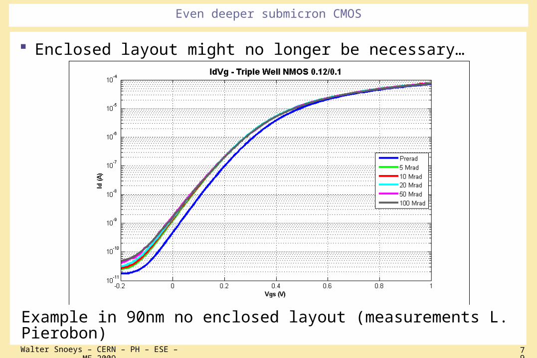
Even deeper submicron CMOS
Enclosed layout might no longer be necessary…
Example in 90nm no enclosed layout (measurements L. Pierobon)
Walter Snoeys – CERN – PH – ESE – ME-2009 80
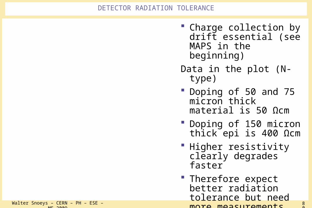
DETECTOR RADIATION TOLERANCE
Charge collection by drift essential (see MAPS in the beginning)
Data in the plot (N-type) Doping of 50 and 75 micron
thick material is 50 Ωcm Doping of 150 micron thick
epi is 400 Ωcm Higher resistivity clearly
degrades faster Therefore expect better
radiation tolerance but need more measurements
Jan 13 2010 p 8181
Conclusions
Perspective for monolithic in standard deep submicron with several advantages
Analog power can be reduced by segmentation and device design Need work on digital (and the analog !), would like to exploit having all
bits at the bottom of the matrix Possibility for prototyping with MPW in 90nm even on more lightly
doped substrates Is very much work in progress In general power will be key to reduce the material Several aspects : device design, processing, circuit design Radiation tolerance: going to very deep submicron is an advantage,
need charge collection by drift

Jan 13 2010 p 8282
THANK YOU