Embed Size (px)
Citation preview
NotesA. Performance and quality attributes and conditions not expressly stated in this specification document are intended to be excluded and do not form a part of this specification document. B. Electrical specifications and performance data contained in this specification document are based on Mini-Circuit’s applicable established test performance criteria and measurement instructions. C. The parts covered by this specification document are subject to Mini-Circuits standard limited warranty and terms and conditions (collectively, “Standard Terms”); Purchasers of this part are entitled to the rights and benefits contained therein. For a full statement of the Standard Terms and the exclusive rights and remedies thereunder, please visit Mini-Circuits’ website at www.minicircuits.com/MCLStore/terms.jsp
Mini-Circuits®
www.minicircuits.com P.O. Box 350166, Brooklyn, NY 11235-0003 (718) 934-4500 [email protected]
Product Features
Typical Applications
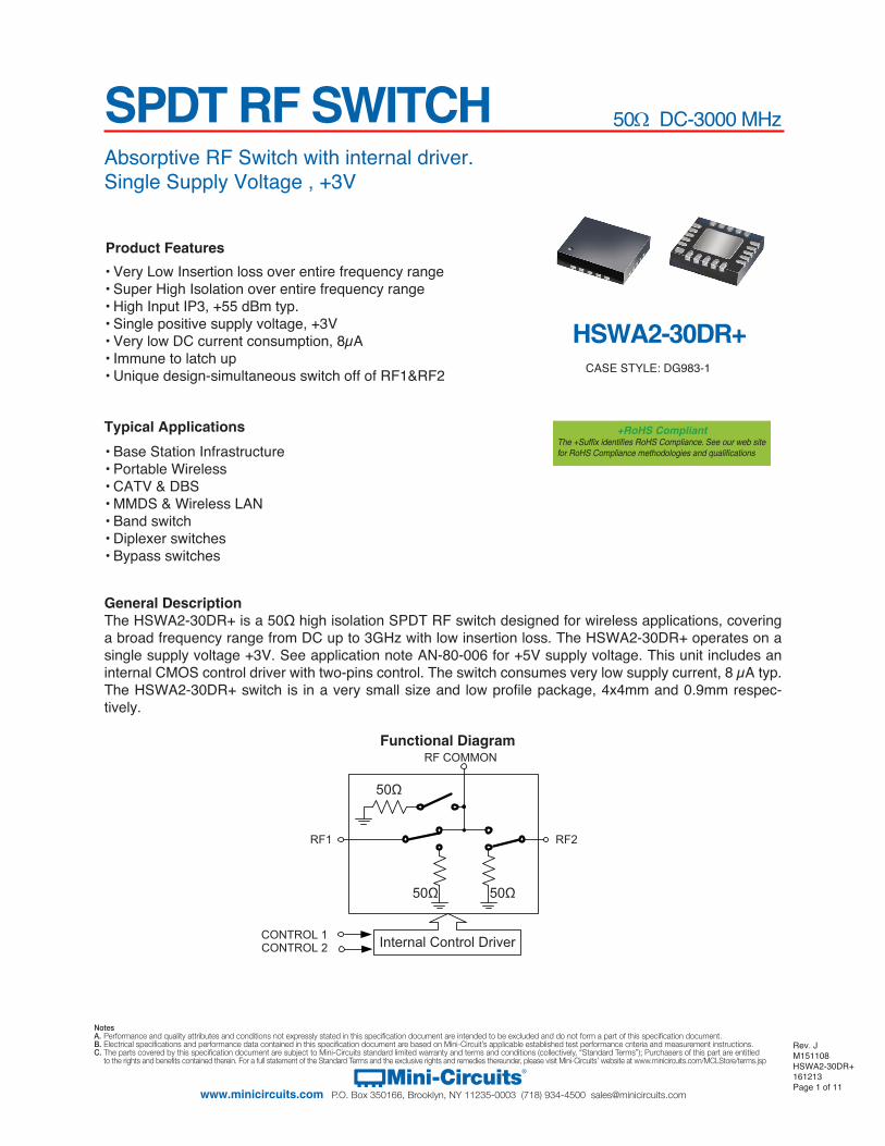
General DescriptionThe HSWA2-30DR+ is a 50Ω high isolation SPDT RF switch designed for wireless applications, covering a broad frequency range from DC up to 3GHz with low insertion loss. The HSWA2-30DR+ operates on a single supply voltage +3V. See application note AN-80-006 for +5V supply voltage. This unit includes an internal CMOS control driver with two-pins control. The switch consumes very low supply current, 8 µA typ. The HSWA2-30DR+ switch is in a very small size and low profile package, 4x4mm and 0.9mm respec-tively.
SPDT RF SWITCH Absorptive RF Switch with internal driver.Single Supply Voltage , +3V
50W DC-3000 MHz
Functional Diagram
50Ω
50Ω
SW3SW2
SW4SW1
50ΩRF
COMMON
RF1
RF2
Control 1 Control 2
CONTROLDRIVER
50Ω
50Ω 50Ω
CONTROL 1CONTROL 2 Internal Control Driver
RF COMMON
RF1 RF2
HSWA2-30DR+
Rev. JM151108HSWA2-30DR+161213Page 1 of 11
• Very Low Insertion loss over entire frequency range• Super High Isolation over entire frequency range • High Input IP3, +55 dBm typ.• Single positive supply voltage, +3V • Very low DC current consumption, 8µA• Immune to latch up• Unique design-simultaneous switch off of RF1&RF2
• Base Station Infrastructure• Portable Wireless• CATV & DBS• MMDS & Wireless LAN• Band switch• Diplexer switches• Bypass switches
CASE STYLE: DG983-1
+RoHS CompliantThe +Suffix identifies RoHS Compliance. See our web site for RoHS Compliance methodologies and qualifications

HSWA2-30DR+SPDT RF SWITCH
Page 2 of 11
NotesA. Performance and quality attributes and conditions not expressly stated in this specification document are intended to be excluded and do not form a part of this specification document. B. Electrical specifications and performance data contained in this specification document are based on Mini-Circuit’s applicable established test performance criteria and measurement instructions. C. The parts covered by this specification document are subject to Mini-Circuits standard limited warranty and terms and conditions (collectively, “Standard Terms”); Purchasers of this part are entitled to the rights and benefits contained therein. For a full statement of the Standard Terms and the exclusive rights and remedies thereunder, please visit Mini-Circuits’ website at www.minicircuits.com/MCLStore/terms.jsp
Mini-Circuits®
www.minicircuits.com P.O. Box 350166, Brooklyn, NY 11235-0003 (718) 934-4500 [email protected]
RF Electrical Specifications, DC-3000 MHz, TAMB=25°C, VDD=+3VParameter Condition Min. Typ. Max. Units
Operating Frequency DC(note 4) 3000 MHz
Insertion Loss (note 1)1 GHz 2 GHz 3 GHz
0.75 0.95 1.2
1.01.2 1.4
dB
Isolation between Common port and RF1/RF2 ports1 GHz 2 GHz 3 GHz
55 46 40
64 50 44
dB
Isolation between RF1 and RF2 ports1 GHz 2 GHz 3 GHz
57 54 40
63 60 48
dB
Return Loss @ Common port1 GHz 2 GHz 3 GHz
20 17 14
dB
Return Loss @ RF1/RF2 ports1 GHz 2 GHz 3 GHz
20 18 17
dB
Input IP2 5 MHz - 1000 MHz +80 dBm
Input IP3 (note 2) 10 MHz - 1000MHz1000MHz - 3000MHz
+55+52
dBm
Input 1dB Compression (note 2,3) 1000 MHz +29 +31 dBm
Notes: 1. I.LOSS values are de-embedded from test board Loss.2. Device linearity degrades below 1 MHz.3. Note absolute maximum ratings for input power.4. Lowest Freq. determined by value of coupling capacitors at RF ports.
Note 8: See Truth Table on page 3.
Parameter Ratings
Operating Temperature -40°C to 85°C
Storage Temperature -65°C to 150°C
Vdd, Supply Voltage -0.3V Min., 4V Max.
Voltage control -0.3V Min., Vdd + 0.3V Max.
ESD, HBM (ANSI/ESD STM 5.1 - 2001) 250V to < 500V (CLASS 1A)
ESD, MM (ANSI/ESD STM 5.2 - 1999) 50V (CLASS M1)
RF input power: (note 8)
When the common port is connected to the RF port (RF1 or RF2)
When the RF port (RF1 or RF2) is not connected to the common port
When the common port is not connected to either RF1 or RF2
+33dBm
+24dBm
+24dBm
Absolute Maximum Ratings
Parameter Min. Typ. Max. Units
Vdd, Supply Voltage(note 5) 2.7 3 3.3 V
Supply Current (Vdd = 3V)(note 6) — 8 20 µA
Control Voltage Low 0 — 0.3xVdd V
Control Voltage High 0.7xVdd — Vdd V
DC Electrical Specifications
Parameter Min. Typ. Max. Units
Switching Time, 50% CTRL to 90/10% RF — 2.0 — µSec
Video Feedthrough, 5 MHz - 1000 MHz (note 7) — — 15 mVp-p
Switching Specifications
Note 7: Measured with a 1 nSec risetime,0/3V pulse and 500 MHz bandwidth.
Note 5: See application note AN-80-006 for +5V supply voltage.Note 6: At Control Frequency of 1 kHz. Increases to 21 µA at 10 kHz and 56 µA at 50 kHz typically.
Permanent damage may occur if any of these limits are exceeded.

HSWA2-30DR+SPDT RF SWITCH
Page 3 of 11
NotesA. Performance and quality attributes and conditions not expressly stated in this specification document are intended to be excluded and do not form a part of this specification document. B. Electrical specifications and performance data contained in this specification document are based on Mini-Circuit’s applicable established test performance criteria and measurement instructions. C. The parts covered by this specification document are subject to Mini-Circuits standard limited warranty and terms and conditions (collectively, “Standard Terms”); Purchasers of this part are entitled to the rights and benefits contained therein. For a full statement of the Standard Terms and the exclusive rights and remedies thereunder, please visit Mini-Circuits’ website at www.minicircuits.com/MCLStore/terms.jsp
Mini-Circuits®
www.minicircuits.com P.O. Box 350166, Brooklyn, NY 11235-0003 (718) 934-4500 [email protected]
The RF switch control bits select the desired switch-state, as shown in Table 1: Truth Table.
STATEControl Input RF Input / Output
Control 1 Control 2 RF1 to RF COMMON RF2 to RF COMMON1 Low Low OFF OFF
2 Low High OFF ON
3 High Low ON OFF
4 High High N/A N/A
EXAMPLE OF STATE 3
Functional Diagram
50Ω
50Ω
SW3SW2
SW4SW1
50ΩRF
COMMON
RF1
RF2
Control 1 Control 2
CONTROLDRIVER
50Ω
50Ω 50Ω
CONTROL 1CONTROL 2 Internal Control Driver
RF COMMON
RF1 RF2
Table 1: Truth Table.
General notes: 1. When either of the RF1 or RF2 ports is closed (ON state), the closed port is connected to the RF Common port.2. When either of the RF1 or RF2 ports is open (OFF state), the open port is connected to an internal 50Ω termination.3. When both RF1 and RF2 ports are open (OFF state), the all three RF ports are connected to an internal 50Ω termination.

HSWA2-30DR+SPDT RF SWITCH
Page 4 of 11
NotesA. Performance and quality attributes and conditions not expressly stated in this specification document are intended to be excluded and do not form a part of this specification document. B. Electrical specifications and performance data contained in this specification document are based on Mini-Circuit’s applicable established test performance criteria and measurement instructions. C. The parts covered by this specification document are subject to Mini-Circuits standard limited warranty and terms and conditions (collectively, “Standard Terms”); Purchasers of this part are entitled to the rights and benefits contained therein. For a full statement of the Standard Terms and the exclusive rights and remedies thereunder, please visit Mini-Circuits’ website at www.minicircuits.com/MCLStore/terms.jsp
Mini-Circuits®
www.minicircuits.com P.O. Box 350166, Brooklyn, NY 11235-0003 (718) 934-4500 [email protected]
Function Pin Number Description
GND 1 RF Ground
GND 2 RF Ground
RF1 3 RF I/O (note 1)
GND 4 RF Ground
GND 5 RF Ground
GND 6 RF Ground
GND 7 RF Ground
RF COM 8 RF Common (note 1)
GND 9 RF Ground
GND 10 RF Ground
GND 11 RF Ground
GND 12 RF Ground
RF2 13 RF I/O (note 1)
GND 14 RF Ground
GND 15 RF Ground
Control 2 16 Control 2
Control 1 17 Control 1
GND 18 Supply Voltage Ground
GND 19 Digital Ground
VDD 20 Supply Voltage
GND Paddle RF Ground Pad (note 2)
Notes:1. RF pins 3, 8 and 13 must be at 0 VDC. The RF pins do not require DC blocking capacitors for proper operation if the 0 VDC requirement is met.
2. The exposed solder pad on the bottom of the package (See Pin Configuration) must be grounded for proper device operation
Pin Description
GNDGND
GN
D
VSS
/GN
D
RF2
GN
D
GN
D
RFC
GN
D
GND
GND
GND
GNDRF1
GNDGND
CTR
L2
CTR
L1
GN
DV
DD
15
14
13
12
11
1
2
3
4
5
6 7 8 9
20 19 18 17 1610
GNDGND
GN
D
GN
D
GND
VD
D
VD
D
PUP
2PU
P1
RFoutC8
LEGND
N/CRFin
C16
C4
C2
C1
C0.
5
2x2mmPaddleground
15
14
13
12
11
1
2
3
4
56 7 8 9 10
20 19 18 17 16
GND
GNDGND
GN
D
GN
D
RF2
GN
D
GN
D
RF
CO
MG
ND
GND
GND
GND
GNDRF1
GNDGND
Con
trol
2C
ontr
ol 1
GN
DVD
D
15
14
13
12
11
1
2
3
4
5
6 7 8 9
20 19 18 17 1610
2x2mmPaddleground
Pin Configuration (Top View)

HSWA2-30DR+SPDT RF SWITCH
Page 5 of 11
NotesA. Performance and quality attributes and conditions not expressly stated in this specification document are intended to be excluded and do not form a part of this specification document. B. Electrical specifications and performance data contained in this specification document are based on Mini-Circuit’s applicable established test performance criteria and measurement instructions. C. The parts covered by this specification document are subject to Mini-Circuits standard limited warranty and terms and conditions (collectively, “Standard Terms”); Purchasers of this part are entitled to the rights and benefits contained therein. For a full statement of the Standard Terms and the exclusive rights and remedies thereunder, please visit Mini-Circuits’ website at www.minicircuits.com/MCLStore/terms.jsp
Mini-Circuits®
www.minicircuits.com P.O. Box 350166, Brooklyn, NY 11235-0003 (718) 934-4500 [email protected]
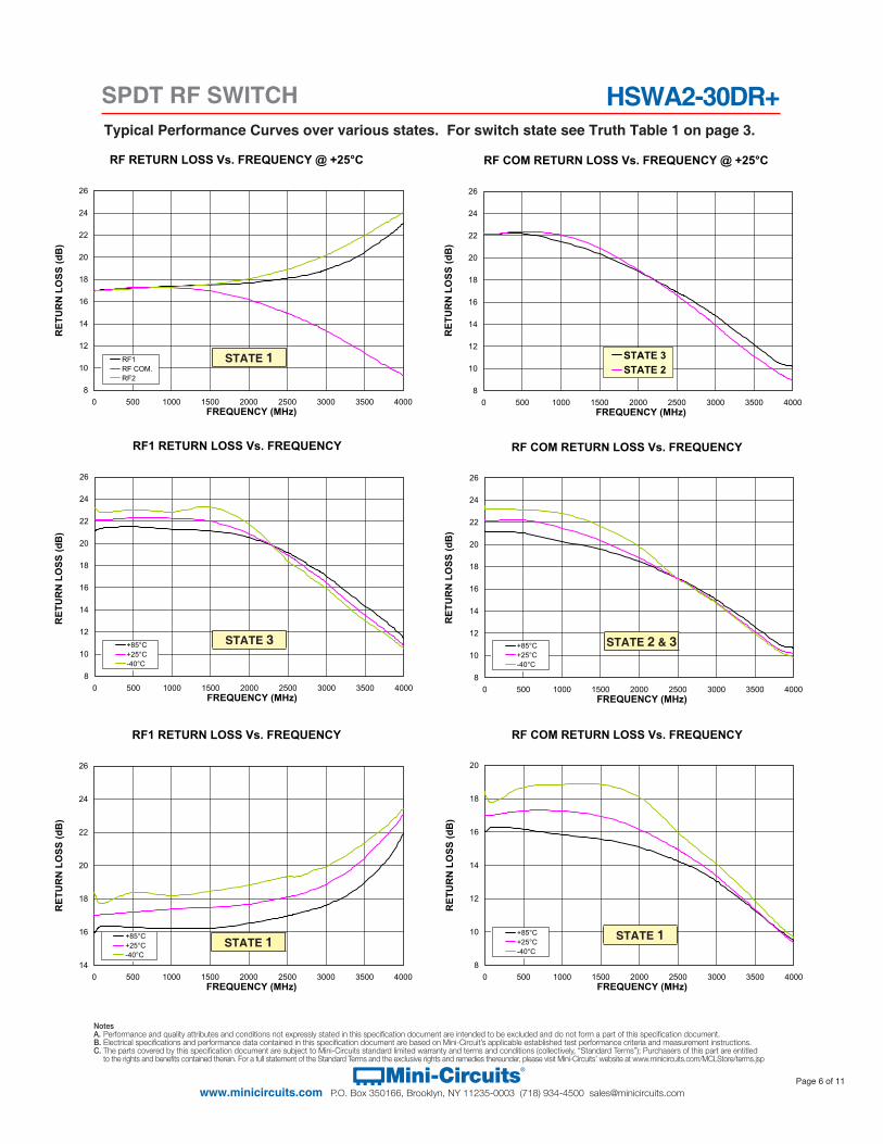
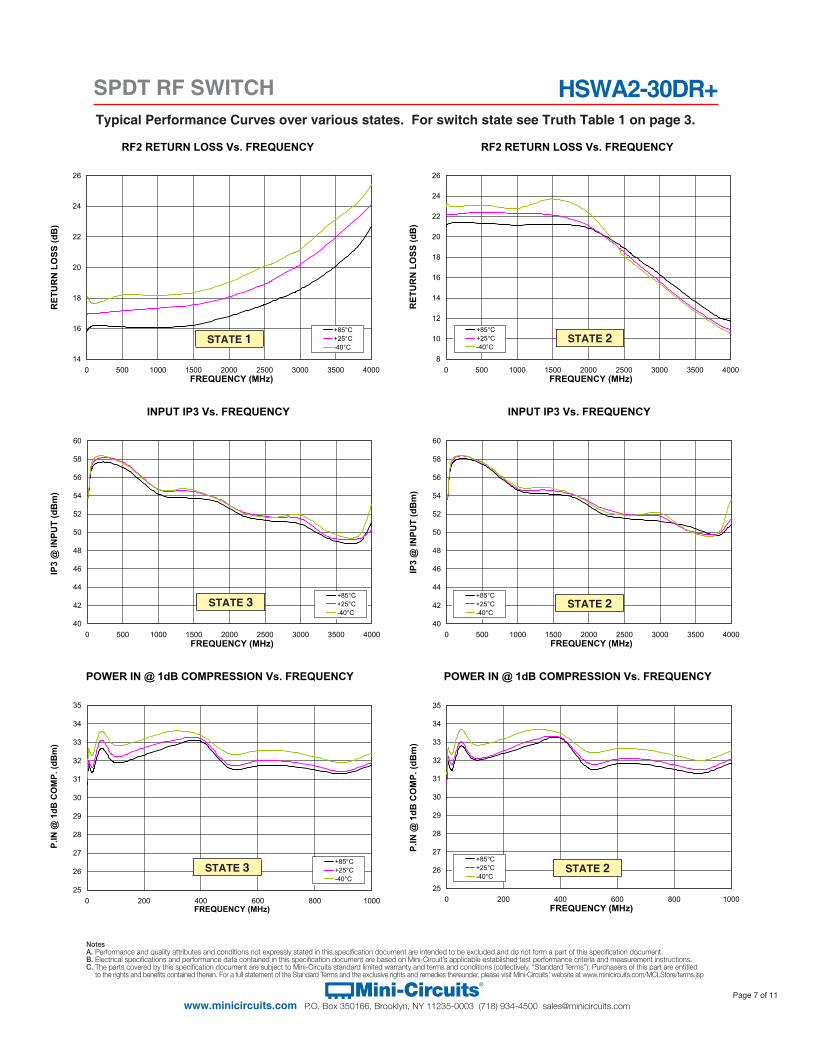
Typical Performance Curves over various states. For switch state see Truth Table 1 on page 3.
INSERTION LOSS Vs. FREQUENCY @ +25°C
0
0.5
1
1.5
2
2.5
0 500 1000 1500 2000 2500 3000 3500 4000FREQUENCY (MHz)
INSE
RTI
ON
LO
SS (d
B)
STATE 3STATE 2
INSERTION LOSS Vs. FREQUENCY
0
0.5
1
1.5
2
2.5
0 500 1000 1500 2000 2500 3000 3500 4000FREQUENCY (MHz)
INSE
RTI
ON
LO
SS (d
B)
+85°C+25°C-40°C
ISOLATION BETWEEN RF1/RF2 TO RF COM Vs. FREQUENCY
30
40
50
60
70
80
90
100
110
120
0 500 1000 1500 2000 2500 3000 3500 4000FREQUENCY (MHz)
ISO
LATI
ON
(dB
)
+85°C+25°C-40°C
ISOLATION BETWEEN RF1/RF2 TO RF COM Vs. FREQUENCY
30
40
50
60
70
80
90
100
110
120
0 500 1000 1500 2000 2500 3000 3500 4000FREQUENCY (MHz)
ISO
LATI
ON
(dB
)
+85°C+25°C-40°C
ISOLATION BETWEEN RF1 TO RF2 Vs. FREQUENCY
30
50
70
90
110
0 500 1000 1500 2000 2500 3000 3500 4000FREQUENCY (MHz)
ISO
LATI
ON
(dB
)
+85°C+25°C-40°C
ISOLATION BETWEEN RF1 TO RF2Vs. FREQUENCY
40
60
80
100
120
140
0 500 1000 1500 2000 2500 3000 3500 4000FREQUENCY (MHz)
ISO
LATI
ON
(dB
)
+85°C+25°C-40°C
STATE 3
STATE 2 & 3 STATE 1
STATE 2 & 3 STATE 1
HSWA2-30DR+SPDT RF SWITCH
Page 6 of 11
NotesA. Performance and quality attributes and conditions not expressly stated in this specification document are intended to be excluded and do not form a part of this specification document. B. Electrical specifications and performance data contained in this specification document are based on Mini-Circuit’s applicable established test performance criteria and measurement instructions. C. The parts covered by this specification document are subject to Mini-Circuits standard limited warranty and terms and conditions (collectively, “Standard Terms”); Purchasers of this part are entitled to the rights and benefits contained therein. For a full statement of the Standard Terms and the exclusive rights and remedies thereunder, please visit Mini-Circuits’ website at www.minicircuits.com/MCLStore/terms.jsp
Mini-Circuits®
www.minicircuits.com P.O. Box 350166, Brooklyn, NY 11235-0003 (718) 934-4500 [email protected]
Typical Performance Curves over various states. For switch state see Truth Table 1 on page 3.
RF RETURN LOSS Vs. FREQUENCY @ +25°C
8
10
12
14
16
18
20
22
24
26
0 500 1000 1500 2000 2500 3000 3500 4000FREQUENCY (MHz)
RET
UR
N L
OSS
(dB
)
RF1RF COM.RF2
RF COM RETURN LOSS Vs. FREQUENCY
8
10
12
14
16
18
20
0 500 1000 1500 2000 2500 3000 3500 4000FREQUENCY (MHz)
RET
UR
N L
OSS
(dB
)
+85°C+25°C-40°C
RF COM RETURN LOSS Vs. FREQUENCY @ +25°C
8
10
12
14
16
18
20
22
24
26
0 500 1000 1500 2000 2500 3000 3500 4000FREQUENCY (MHz)
RET
UR
N L
OSS
(dB
)
STATE 3STATE 2
RF COM RETURN LOSS Vs. FREQUENCY
8
10
12
14
16
18
20
22
24
26
0 500 1000 1500 2000 2500 3000 3500 4000FREQUENCY (MHz)
RET
UR
N L
OSS
(dB
)
+85°C+25°C-40°C
RF1 RETURN LOSS Vs. FREQUENCY
14
16
18
20
22
24
26
0 500 1000 1500 2000 2500 3000 3500 4000FREQUENCY (MHz)
RET
UR
N L
OSS
(dB
)
+85°C+25°C-40°C
RF1 RETURN LOSS Vs. FREQUENCY
8
10
12
14
16
18
20
22
24
26
0 500 1000 1500 2000 2500 3000 3500 4000FREQUENCY (MHz)
RET
UR
N L
OSS
(dB
)
+85°C+25°C-40°C
STATE 1
STATE 1
STATE 2 & 3STATE 3
STATE 1
HSWA2-30DR+SPDT RF SWITCH
Page 7 of 11
NotesA. Performance and quality attributes and conditions not expressly stated in this specification document are intended to be excluded and do not form a part of this specification document. B. Electrical specifications and performance data contained in this specification document are based on Mini-Circuit’s applicable established test performance criteria and measurement instructions. C. The parts covered by this specification document are subject to Mini-Circuits standard limited warranty and terms and conditions (collectively, “Standard Terms”); Purchasers of this part are entitled to the rights and benefits contained therein. For a full statement of the Standard Terms and the exclusive rights and remedies thereunder, please visit Mini-Circuits’ website at www.minicircuits.com/MCLStore/terms.jsp
Mini-Circuits®
www.minicircuits.com P.O. Box 350166, Brooklyn, NY 11235-0003 (718) 934-4500 [email protected]
Typical Performance Curves over various states. For switch state see Truth Table 1 on page 3.
RF2 RETURN LOSS Vs. FREQUENCY
14
16
18
20
22
24
26
0 500 1000 1500 2000 2500 3000 3500 4000FREQUENCY (MHz)
RET
UR
N L
OSS
(dB
)
+85°C+25°C-40°C
RF2 RETURN LOSS Vs. FREQUENCY
8
10
12
14
16
18
20
22
24
26
0 500 1000 1500 2000 2500 3000 3500 4000FREQUENCY (MHz)
RET
UR
N L
OSS
(dB
)
+85°C+25°C-40°C
INPUT IP3 Vs. FREQUENCY
40
42
44
46
48
50
52
54
56
58
60
0 500 1000 1500 2000 2500 3000 3500 4000FREQUENCY (MHz)
IP3
@ IN
PUT
(dB
m)
+85°C+25°C-40°C
INPUT IP3 Vs. FREQUENCY
40
42
44
46
48
50
52
54
56
58
60
0 500 1000 1500 2000 2500 3000 3500 4000FREQUENCY (MHz)
IP3
@ IN
PUT
(dB
m)
+85°C+25°C-40°C
POWER IN @ 1dB COMPRESSION Vs. FREQUENCY
25
26
27
28
29
30
31
32
33
34
35
0 200 400 600 800 1000FREQUENCY (MHz)
P.IN
@ 1
dB C
OM
P. (d
Bm
)
+85°C+25°C-40°C
POWER IN @ 1dB COMPRESSION Vs. FREQUENCY
25
26
27
28
29
30
31
32
33
34
35
0 200 400 600 800 1000FREQUENCY (MHz)
P.IN
@ 1
dB C
OM
P. (d
Bm
)
+85°C+25°C-40°C
STATE 1 STATE 2
STATE 2
STATE 2STATE 3
STATE 3

HSWA2-30DR+SPDT RF SWITCH
Page 8 of 11
NotesA. Performance and quality attributes and conditions not expressly stated in this specification document are intended to be excluded and do not form a part of this specification document. B. Electrical specifications and performance data contained in this specification document are based on Mini-Circuit’s applicable established test performance criteria and measurement instructions. C. The parts covered by this specification document are subject to Mini-Circuits standard limited warranty and terms and conditions (collectively, “Standard Terms”); Purchasers of this part are entitled to the rights and benefits contained therein. For a full statement of the Standard Terms and the exclusive rights and remedies thereunder, please visit Mini-Circuits’ website at www.minicircuits.com/MCLStore/terms.jsp
Mini-Circuits®
www.minicircuits.com P.O. Box 350166, Brooklyn, NY 11235-0003 (718) 934-4500 [email protected]
Outline Drawing (DG983-1)
Device Marking
Outline Dimensions ( )inchmm
A B C D E F G H J K L M N P Q R WT. GRAMS
.157 .157 .035 .008 .081 .081 .010 — .022 .020 .177 .177 .081 .010 .032 .081.04
4.00 4.00 0.90 0.20 2.06 2.06 0.25 — 0.56 0.50 4.50 4.50 2.06 0.25 0.81 2.06
Suggested Layout, Tolerance to be within ±.002
PCB Land Pattern
MCLHSWA2
+
Pin 1Index

HSWA2-30DR+SPDT RF SWITCH
Page 9 of 11
NotesA. Performance and quality attributes and conditions not expressly stated in this specification document are intended to be excluded and do not form a part of this specification document. B. Electrical specifications and performance data contained in this specification document are based on Mini-Circuit’s applicable established test performance criteria and measurement instructions. C. The parts covered by this specification document are subject to Mini-Circuits standard limited warranty and terms and conditions (collectively, “Standard Terms”); Purchasers of this part are entitled to the rights and benefits contained therein. For a full statement of the Standard Terms and the exclusive rights and remedies thereunder, please visit Mini-Circuits’ website at www.minicircuits.com/MCLStore/terms.jsp
Mini-Circuits®
www.minicircuits.com P.O. Box 350166, Brooklyn, NY 11235-0003 (718) 934-4500 [email protected]
Recommended layout for PCB design
The amount of vias surrounding the device in the suggested PCB layout are critical for obtaining the speci-fied isolation performance for the device shown in the datasheet.
Suggested Layout for PCB Design (PL-206)

HSWA2-30DR+SPDT RF SWITCH
Page 10 of 11
NotesA. Performance and quality attributes and conditions not expressly stated in this specification document are intended to be excluded and do not form a part of this specification document. B. Electrical specifications and performance data contained in this specification document are based on Mini-Circuit’s applicable established test performance criteria and measurement instructions. C. The parts covered by this specification document are subject to Mini-Circuits standard limited warranty and terms and conditions (collectively, “Standard Terms”); Purchasers of this part are entitled to the rights and benefits contained therein. For a full statement of the Standard Terms and the exclusive rights and remedies thereunder, please visit Mini-Circuits’ website at www.minicircuits.com/MCLStore/terms.jsp
Mini-Circuits®
www.minicircuits.com P.O. Box 350166, Brooklyn, NY 11235-0003 (718) 934-4500 [email protected]
How to use evaluation Board TB-347
The Evaluation board TB-347 was designed to evaluate the electrical performance of the HSWA2-30DR+ SPDT switch.
RF3 and RF4 SMA 50Ω connectors are connected through a 50Ω transmission line that is used to estimate the evaluation board loss for de-embedding purposes. The transmission lines were designed using a coplanar wave-guide with ground plane. For details, please see suggested PCB layout on Page 8. The number of vias surrounding the switch is critical for obtaining the specified isolation.
The TB-347 operates from +2.7V to +6.5V applied to VDD connector. IC1 voltage regulator limits the supply voltage to the switch to +3.3V. IC2 is a Schmitt trigger & buffer which prevents an overload of switch control inputs from high level control signals (up to +5.5V) and prevents from noise and transient spikes during switching process.
The control connector is used for computer control mode or manual operation mode. In manual control mode connect Control 1 and/or Control 2 to ground to set Control 1 and/or Control 2 to logic low, respectively. When jumpers are removed, the digital control input pulled up to VDD for logic high.For computer control mode the software & cable are supplied. The cable should be connected between computer LPT port and evaluation board control connector.
TB-347 Evaluation Board Schematic Diagram
TB-347
Bill of MaterialsN# DESCRIPTION QtyN3 Capacitor Tantalum 1206 1µF +/-10% 1
N6 Capacitor X7R 0402 0.01µF +/-10% 1
N7 Capacitor Tantalum 1206 3.3µF +/-10% 1
N8, N9, N17 Capacitor 0603 NPO 100pF +/-5% 3
N11, N14 Resistor 0603 1 MOHM +/-1% 2
N12, N15 Resistor 0603 10 MOHM +/-1% 2
N10, N16 Resistor 0603 10 KOHM +/-1% 2
N5 LDO Voltage Regulator 3.3V MAX8878 1
N13 Dual Non-inverted Schmitt Trigger SN74LVC2G17 1
N1 Empty (location for HSWA2-30DR+) 1
N4 Empty 1

HSWA2-30DR+SPDT RF SWITCH
Page 11 of 11
NotesA. Performance and quality attributes and conditions not expressly stated in this specification document are intended to be excluded and do not form a part of this specification document. B. Electrical specifications and performance data contained in this specification document are based on Mini-Circuit’s applicable established test performance criteria and measurement instructions. C. The parts covered by this specification document are subject to Mini-Circuits standard limited warranty and terms and conditions (collectively, “Standard Terms”); Purchasers of this part are entitled to the rights and benefits contained therein. For a full statement of the Standard Terms and the exclusive rights and remedies thereunder, please visit Mini-Circuits’ website at www.minicircuits.com/MCLStore/terms.jsp
Mini-Circuits®
www.minicircuits.com P.O. Box 350166, Brooklyn, NY 11235-0003 (718) 934-4500 [email protected]
Tape and Reel Packaging Information Table T&R
TRNo.
No. of Devices Reel Size TapeWidth
Pitch Unit Orientation
Small quantity standards 20, 50, 100, 200 7 inch
F873000
(Standard) 13 inch
12 mm 8 mm TapeCavity
Direction of Feed