Embed Size (px)
Citation preview
December 2005
NASA/TP–2005–212792
Spacecraft Thermal Control Coatings References
Lonny Kauder

The NASA STI Program Offi ce … in Profi le
Since its founding, NASA has been ded i cat ed to the ad vance ment of aeronautics and space science. The NASA Sci en tifi c and Technical Information (STI) Pro gram Offi ce plays a key part in helping NASA maintain this im por tant role.
The NASA STI Program Offi ce is operated by Langley Re search Center, the lead center for NASA s scientifi c and technical in for ma tion. The NASA STI Program Offi ce pro vides ac cess to the NASA STI Database, the largest col lec tion of aero nau ti cal and space science STI in the world. The Pro gram Offi ce is also NASA s in sti tu tion al mech a nism for dis sem i nat ing the results of its research and de vel op ment ac tiv i ties. These results are published by NASA in the NASA STI Report Series, which includes the following report types:
• TECHNICAL PUBLICATION. Reports of com plet ed research or a major signifi cant phase of research that present the results of NASA pro-grams and include ex ten sive data or the o ret i cal analysis. Includes com pi la tions of sig nifi cant scientifi c and technical data and in for ma tion deemed to be of con tinu ing ref er ence value. NASA s counterpart of peer-re viewed formal pro fes sion al papers but has less stringent lim i ta -tions on manuscript length and ex tent of graphic pre sen ta tions.
• TECHNICAL MEMORANDUM. Scientifi c and tech ni cal fi ndings that are pre lim i nary or of spe cial ized interest, e.g., quick re lease reports, working papers, and bib li og ra phies that contain minimal annotation. Does not contain extensive analysis.
• CONTRACTOR REPORT. Scientifi c and techni-cal fi ndings by NASA-sponsored con trac tors and grantees.
• CONFERENCE PUBLICATION. Collected pa pers from scientifi c and technical conferences, symposia, sem i nars, or other meet ings spon sored or co spon sored by NASA.
• SPECIAL PUBLICATION. Scientifi c, tech ni cal, or historical information from NASA pro grams, projects, and mission, often con cerned with sub-jects having sub stan tial public interest.
• TECHNICAL TRANSLATION. En glish-language trans la tions of foreign sci en tifi c and tech ni cal ma-terial pertinent to NASA s mis sion.
Specialized services that complement the STI Pro-gram Offi ceʼs diverse offerings include cre at ing custom the sau ri, building customized da ta bas es, organizing and pub lish ing research results . . . even pro vid ing videos.
For more information about the NASA STI Pro gram Offi ce, see the following:
• Access the NASA STI Program Home Page at http://www.sti.nasa.gov/STI-homepage.html
• E-mail your question via the Internet to [email protected]
• Fax your question to the NASA Access Help Desk at (301) 621-0134
• Telephone the NASA Access Help Desk at (301) 621-0390
• Write to: NASA Access Help Desk NASA Center for AeroSpace In for ma tion 7121 Standard Drive Hanover, MD 21076–1320
National Aeronautics and Space Ad min is tra tion
Goddard Space Flight CenterGreenbelt, Maryland 20771
December 2005
NASA/TP–2005–212792
Lonny KauderNASA/Goddard Space Flight Center, Greenbelt, Maryland
Spacecraft Thermal Control Coatings References

Available from:
NASA Center for AeroSpace Information National Technical Information Service7121 Standard Drive 5285 Port Royal RoadHanover, MD 21076-1320 Springfi eld, VA 22161Price Code: A17 Price Code: A10
i
Table of Contents pg
Introduction ... ii I . Electromagnetic Origins of Thermal Properties .... 1 II. Factors that Affect Emittance .... 10
2.1 Change in emittance with Temperature .... 10 2.2 Role of thickness in Effective Emittance .. 11 2.3 Non-Grey Effects .. 12
III. Measurement of Thermal Properties ...... 18
3.1 Solar absorptance .. 18 3.2 Measurement of Emittance ... 23 3.2.1 Infrared Reflectometry ..... 23 3.2.2 Emittance Calculated from Infrared Reflectance Measurements .. 25 3.2.3 Calorimetric Technique for Determining Hemispherical Emittance .... 26 3.2.4 Thermal Balance Method for Determining Hemispherical Emittance .. 27 3.2.5 Methods of Increasing Emittance . 29 3.2.6 Considerations and Lessons Learned .29
3.3 Electrical properties of Thermal Control Coatings.. 30 References... 39 IV. Thermal Control Coatings Data ...... 40
4.1 Black Coatings ...... 40 4.2 White and Color Coatings . 41 4.3 Conductive Paints .. 42 4.4 Anodize Aluminum Coatings .... 43 4.5 Metals and Conversion Coatings ... 44 4.6 Vapor Deposited Coatings ..... 45 4.7 Solar Cells ...... 46 4.8 Composite Coatings ... 47 4.9 Films and Tapes ..... 48
V. Total Hemispherical Reflectance Curves for Selected Thermal Control Coatings .... 50 VI. Total Hemispherical Emittance as a Function of Temperature For Selected Thermal Control Coatings ..... . 90
ii
Introduction The successful thermal design of spacecraft depends in part on a knowledge of the solar absorptance and hemispherical emittance of the thermal control coatings used in & on the spacecraft. The Goddard Space Flight Center has had since its beginning, a group whose mission has been to provide thermal/optical properties data of thermal control coatings to Thermal Engineers. This handbook represents a summary of the data and knowledge accumulated over many years at the GSFC. I would like to thank the many people who have contributed to this data and assisted in the creation of this handbook: Jack Triolo, Wanda Peters, John Henninger, Amani Ginyard, Monali Joshi, & Blake Miller.
1
I. Electromagnetic Origins of Emittance and Reflectance The following is a derivation of the parallel and perpendicular components of reflectivity starting from Maxwells laws. Looking forward to the end result (equation 23 & 24 pg 8 &9) will not affect the understanding of the topic. When electromagnetic energy is incident on an opaque surface such as a typical thermal control coating, part of the energy is reflected back into space and part of the energy is absorbed in the material. Maxwells equations can, at least in theory, be used to describe the interaction of electromagnetic radiation with spacecraft coatings if one happens to know the bulk properties of conductivity, permittivity and permeability of the coating. The following set of well known Maxwell equations (reference 1) are necessary to describe the interaction of electromagnetic energy absorbed or reflected by metals and dielectrics used in thermal control coatings:
E+tE = H
rr
rσξ
∂∂×∇ (1
t
H- = E
∂∂×∇r
rµ
(2
0 = E r
⋅∇ (3
0 = Hr
⋅∇ (4
Where ξ, µ, σ, are the permittivity, permeability and conductivity of the medium respectively. The electric field vector is represented here by E
rand the magnetic field vector by H
r. Applying an appropriate vector identity (reference 3) and
taking the curl of the first two equations and using equations (3 and (4 from above, its clear that the Electric and Magnetic fields must satisfy the following set of vector wave equations:
t
HtHH
∂∂+
∂∂=∇
rrr
σµξµ 2
22 (5
tE
tEE
∂∂+
∂∂=∇
rrr
σµξµ 2
22 (6
Lets assume the general form of an electromagnetic plane wave incident on a surface with a time dependency t and frequency ω:
)(),( trkjoeEtrE ω−⋅=
rrrrr (7
)(),( trkjoeHtrH ω−⋅=
rrrrr (8
where the direction of propagation is given by the unit vector k:
zkykxkk rrrr++=
2
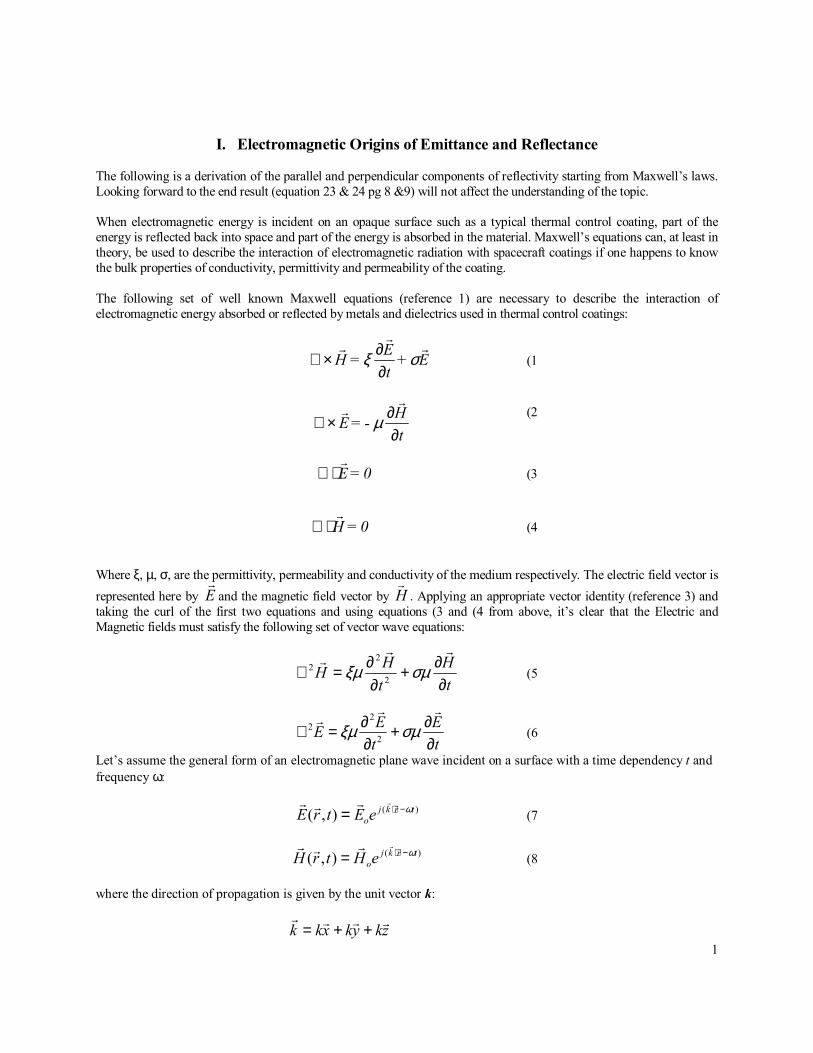
and any given vector is given by r: zryrxrr rrrr ++= where xr , yr , zr are unit vectors in the x,y, and z direction. Now consider the case of an electromagnetic plane wave in space incident on a thermal control surface with conductivity, permeability and permittivity of, σ, µ, and ξ respectively. The following diagrams represents two cases, one in which the electric vector is perpendicular to the normal and the other in which the magnetic vector is perpendicular to the normal.
E ⊥ to plane of incidence E to plane of incidence
Figure 1.1-1. Electromagnetic waves incident on a thermal control coating
Where n is a unit normal vector, 0µ and 0ξ are the permeability and permittivity respectively of space and σ, µ and ξ are the conductivity, permeability and permittivity respectively of the coating. For each case the three waves (incident, reflected and refracted) are represented by:
)(),( trkjoeEtrE ω−⋅=
rrrrr )(),( trkj
oeHtrH ω−⋅=rvrrr
Incident wave
)(),( trkjoeEtrE ϖ−⋅′′=′
rrrrr )(),( trkj
oeHtrH ω−⋅′′=′rrrrr
Reflected wave
)(),( trkjoeEtrE ω−⋅′′′′=′′
rrrrr )(),( trkj
oeHtrH ω−⋅′′′′=′′rrrrr
Refracted wave
The E field and H field for an electromagnetic wave are perpendicular and therefore the E and H components can only satisfy the wave equation provided that:
)(),( trkjoeEtrE ω−⋅=
rrrrr
keEk
trHtrkj
o
o
o)(
),(ω
µξ −⋅×
=rrrr
rr Incident wave
x
z
space
coating
n
refracted beam
reflected beamincident beam
HE
k
E'H'
k"
H"
E"
k'. .
.
x
z
space
coating
n
refracted beam
reflected beamincident beam
H
Ek E'
H'
k"
H"
E"
k'
i i
r
i
r
i
σ µ ξ( , , ) σ µ ξ( , , )
ξ0µ0( , )ξ0µ0
( , )
3
)(),( trkjoeEtrE ω−⋅′′=′
rrrrr
keEk)t,r(H
)trk(jo
o
o
′′×′=′
−⋅′ ω
µξ
rrrrrr
Reflected wave
)(),( trkjoeEtrE ω−⋅′′′′=′′
rrrrr
keEk
jjtrH
trkjo
′′′′×′′+=′′
−⋅′′ )(
),(ω
ωµωξσ
rrrrrr
Refracted wave
Where σ = 0 for space. Electromagnetic waves must meet the appropriate boundary conditions at the space/thermal coating boundary (i.e. the normal components of the displacement vector, D and the magnetic induction vector, B are continuous and the tangential components of the electric field vector, E and the magnetic field vector H are continuous at z=0) (reference 2):
EDrr
ξ= ED oo
rrξ=
HBrr
µ= HB oo
rrµ=
0])([ =⋅′′′′−′+ nEEE ooorrrr
ξξ (9
0=⋅
′′
′′×′′′′
′′+′′−′
′×′+× nk
Ekj
jk
EkkEk oo
o
oo
o
o
oo
rrrrrrr
µωξωσµ
µξµ
µξµ (10
0)( =×′′−′+ nEEE ooorrrr
(11
0=×
′′
′′×′′′′
′′+−′
′×′+× nk
Ekj
jk
EkkEk oo
o
oo
o
o rrrrrrr
µωξωσ
µξ
µξ
(12
The first and second boundary condition for the first case give nothing, since the E field is perpendicular to the page and hence ⊥ to nr . However, from the third boundary condition we have:
0=′′−′+ ooo EEE (13 and the forth boundary condition gives:
0)()()( =′′
×′′×′′′′
′′+−′
×′×′+××k
nEkj
jk
nEkk
nEk oo
o
oo
o
orrrrrrrrr
µωξωσ
µξ
µξ
(14
By using the appropriate vector identity and substituting oE ′′ from equation (13 into equation (14, the ratio of the
incident electric field, oE ′ , to the reflected electric field oE can be obtained:
4
′′
′′++
′′
′′+−=
′
)cos()cos(
)cos()cos(
rj
ji
rj
ji
EE
o
o
o
o
o
o
µωξωσ
µξ
µωξωσ
µξ
(15
To obtain the reflectivity one only needs to multiply the numerator and denominator of this expression by their respective complex conjugates (reference 4). In this case the reflectivity of an electromagnetic wave striking the surface of a thermal control coating with its electric vector perpendicular to the surface normal is:
)(cos)cos()cos(2)(cos
)(cos)cos()cos(2)(cos
22
22
2
222
22
22
2
222
rrii
rrii
µωξωσ
µξ
µωξωσ
µξ
µξ
µωξωσ
µξ
µωξωσ
µξ
µξ
ρ
′′′′++
′′′′
+′′
′′++
′′′′++
′′′′
+′′
′′+−=⊥
Now for the second case, where the magnetic field, H, is pointing out of the page (i.e. H ⊥ to plane of incidence) the 3rd boundary condition gives:
0)cos()cos()cos( =′′+′+− rEiEiE ooo (16
And the forth boundary condition gives:
0=×
′′
′′×′′′′
′′+−′
′×′+× nk
Ekj
jk
EkkEk oo
o
oo
o
o rrrrrrr
µωξωσ
µξ
µξ
(17
Again, using the appropriate vector identity and substituting for oE ′′ from equation (15 into equation (17, we get the
ratio of the incident electric field, oE ′ , to the reflected electric field oE for the parallel case:
)cos()cos(
)cos()cos(
ij
jr
ij
jr
EE
o
o
o
o
o
o
µωξωσ
µξ
µωξωσ
µξ
′′′′++
′′′′++−
=′
(18
The reflectivity for an electromagnetic wave striking the surface of a thermal control coating with its electric vector parallel to the surface normal is then just the numerator and denominator of this expression multiplied by their respective complex conjugates:
5
)(cos)cos()cos(2)(cos
)(cos)cos()cos(2)(cos
22
222
2
22
22
222
2
22
rrii
rrii
µξ
µξ
µωξωσ
µξ
µωξωσ
µξ
µξ
µωξωσ
µξ
µωξωσ
ρ
+′′′′
+′′
′′++′′
′′+
+′′′′
+′′
′′+−′′
′′+
= (19
It is however, useful to cast the entire equation in terms of the angle of incident. This can be accomplished by noting that the phase factors must of necessity all be equal at the boundary z=0, therefore:
000 )()()( === ⋅′′=⋅′=⋅ zzz xkxkxk rrrrrr (20
Where upon inserting the values for k and k ′′
)sin()sin( 422
222
riµω
σξωµξ
′′+′′
= (21
This can be put in terms of cos(r) by solving for sin(r) and using a common trigonometric identity giving:
)(sin1)cos( 2
222ir
σξω
µωµξ
+′′
′′−= (22
Then the perpendicular and parallel components of reflectivity in terms of angle of incident become:
+′′
′′−+
+′′
′′−
′′′′
+′′
′′++′′
′′+
+′′
′′−+
+′′
′′−
′′′′
+′′
′′+−′′
′′+
=
)(sin1)(sin1)cos(2)(cos
)(sin1)(sin1)cos(2)(cos
2
222
2
2222
222
2
22
2
222
2
2222
222
2
22
iiii
iiii
σξω
µωµξ
µξ
σξω
µωµξ
µξ
µωξωσ
µξ
µωξωσ
σξω
µωµξ
µξ
σξω
µωµξ
µξ
µωξωσ
µξ
µωξωσ
ρ
(23
and;
+′′
′′−
′′′′++
+′′
′′−
′′′′
+′′
′′++
+′′
′′−
′′′′++
+′′
′′−
′′′′
+′′
′′+−
=⊥
)(sin1)(sin1)cos(2)(cos
)(sin1)(sin1)cos(2)(cos
2
2222
222
2222
222
2
2222
222
2222
222
iiii
iiii
σξω
µωµξ
µωξωσ
σξω
µωµξ
µξ
µωξωσ
µξ
µξ
σξω
µωµξ
µωξωσ
σξω
µωµξ
µξ
µωξωσ
µξ
µξ
ρ (24
Then the total reflectivity as a function of the angle of incident and the fundamental properties of the coating is just the average of the parallel and perpendicular reflectance components:
6
2),',,,,(
⊥+=′
ρρβξµσξµρ oo (25
(Where β has been used here for angle of incident instead of i, for the sake of conformity) The absorptance, reflectance and transmittance must of course sum to unity.
1=++ tρα (26 If the material is opaque (t =0) and the absorptance is equal to the emittance (as is generally accepted) then the directional emissivity can be found by substituting the reflectance of the coating from (25:
),',,,,(1),',,,,( βξµσξµρβξµσξµε ′′−=′′ oooo (27 The emittance as a function of angle of incidence can now be determined for any given set of permittivity, conductivity, permeability and wavelength. The index of refraction for the material can also be found using these same values in the equation below:
++−+
++=
22
112
112 ωξ
σµξωξσµξ in (28
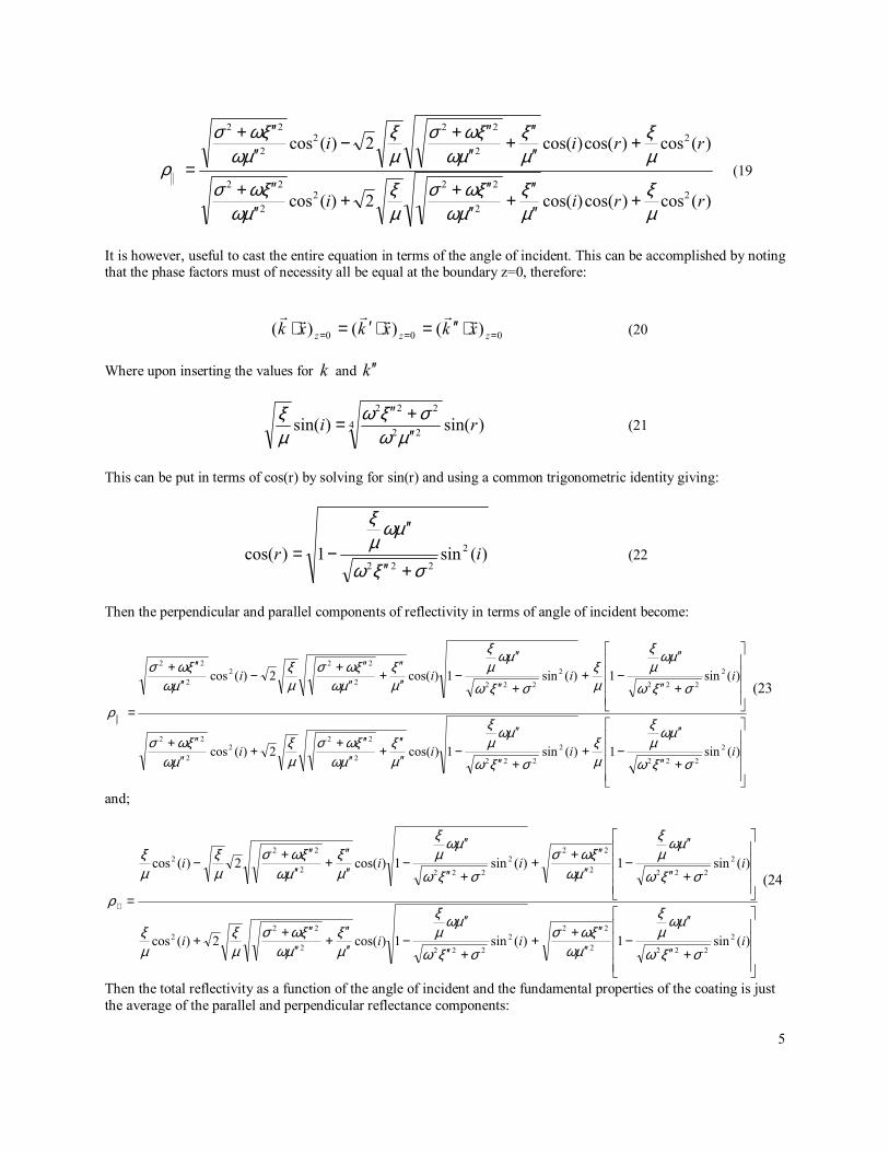
Choosing values of conductivity, permeability and permittivity for a dielectric material coating that gives a real index of refraction equal to approximately 1.5, a directional emissivity graph can be plotted for this hypothetical, but somewhat typical, dielectric coating:
0 0.2 0.4 0.6 0.8 1.00.20.40.60.81.0
0 1020
30
40
50
60
70
80
90
1020
30
40
50
60
70
80
90
Directional Emissivity
Angle of Emission
ε (β)
β
Figure 1.1-2. Directional emissivity curve for a dielectric with an index of refraction of n=1.5 This differs from a Lambertian radiator, which would have no change in emissivity as a function of angle. In real materials the emissivity drops considerably at large angles of β as can be seen in the above graph.
7
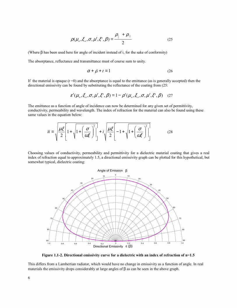
When a material is conductive however, such as a metal, the directional emissivity curve has a somewhat different shape than the dielectric case:
0 0.1 0.2 0.3 0.4 0.50.10.20.30.40.5
0 1020
30
40
50
60
70
80
90
1020
30
40
50
60
70
80
90
Directional Emissivity
Angle of Emission
ε (β)
β
Figure 1.1-3. Directional emissivity curve for a conductor with an index of refraction of n= 5.7+i9.7
This graph shows that the peak emissivity, rather than occurring at near normal to the material, as in the dielectric case, now occurs at very large angles but still drops to zero as the angle β approaches 90 degrees. It is often easier to measure the normal emittance of a material than it is to measure the total hemispherical emittance. It is therefore useful to calculate the ratio of these two quantities so that a reasonable conversion can be made when only the normal emittance is unknown. To obtain the total hemispherical emittance, the emittance as a function of angle must be integrated over the entire hemisphere.
∫π
ωβθβεπ
ε2
0
cos d),,(1=H (29
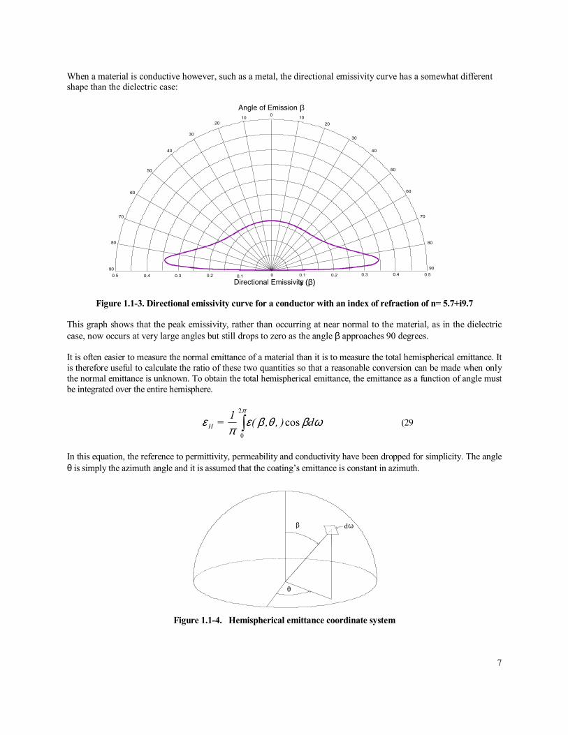
In this equation, the reference to permittivity, permeability and conductivity have been dropped for simplicity. The angle θ is simply the azimuth angle and it is assumed that the coatings emittance is constant in azimuth.
β
θ
dω
Figure 1.1-4. Hemispherical emittance coordinate system
8
The ratio of hemispherical emittance to normal emittance is then just:
),,(
d),,(1
=n
H
0
cos2
0
βε
ωβθβεπ
εε
π
∫ (30
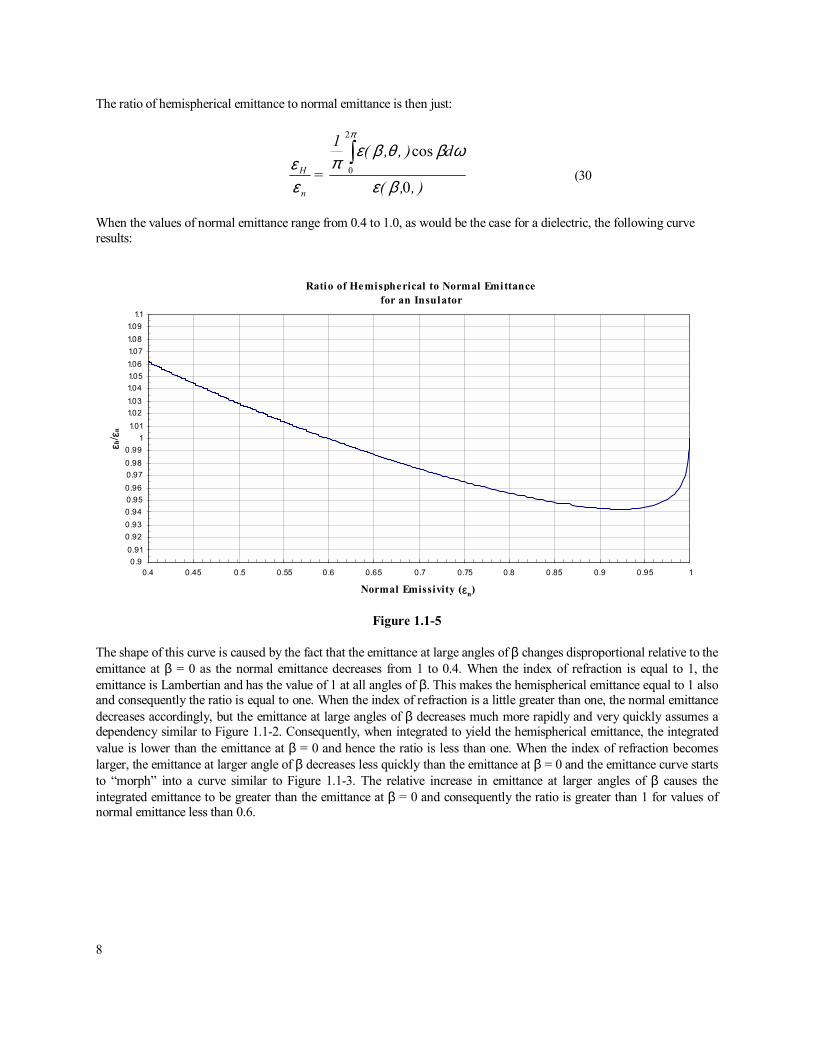
When the values of normal emittance range from 0.4 to 1.0, as would be the case for a dielectric, the following curve results:
Ratio of Hemispherical to Normal Emittance for an Insulator
0.90.91
0.920.930.940.950.960.970.980.99
11.011.021.031.041.051.061.071.081.09
1.1
0.4 0.45 0.5 0.55 0.6 0.65 0.7 0.75 0.8 0.85 0.9 0.95 1
Normal Emissivity (εn)
εh/ ε
n
Figure 1.1-5 The shape of this curve is caused by the fact that the emittance at large angles of β changes disproportional relative to the emittance at β = 0 as the normal emittance decreases from 1 to 0.4. When the index of refraction is equal to 1, the emittance is Lambertian and has the value of 1 at all angles of β. This makes the hemispherical emittance equal to 1 also and consequently the ratio is equal to one. When the index of refraction is a little greater than one, the normal emittance decreases accordingly, but the emittance at large angles of β decreases much more rapidly and very quickly assumes a dependency similar to Figure 1.1-2. Consequently, when integrated to yield the hemispherical emittance, the integrated value is lower than the emittance at β = 0 and hence the ratio is less than one. When the index of refraction becomes larger, the emittance at larger angle of β decreases less quickly than the emittance at β = 0 and the emittance curve starts to morph into a curve similar to Figure 1.1-3. The relative increase in emittance at larger angles of β causes the integrated emittance to be greater than the emittance at β = 0 and consequently the ratio is greater than 1 for values of normal emittance less than 0.6.
9
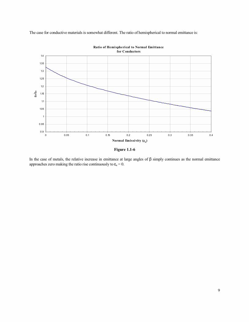
The case for conductive materials is somewhat different. The ratio of hemispherical to normal emittance is:
Ratio of Hemispherical to Normal Emittance for Conductors
0.9
0.95
1
1.05
1.1
1.15
1.2
1.25
1.3
1.35
1.4
0 0.05 0.1 0.15 0.2 0.25 0.3 0.35 0.4
Normal Emissivity (εn)
εh/ ε
n
Figure 1.1-6 In the case of metals, the relative increase in emittance at large angles of β simply continues as the normal emittance approaches zero making the ratio rise continuously to εn = 0.
10
II. Factors that Affect Emittance
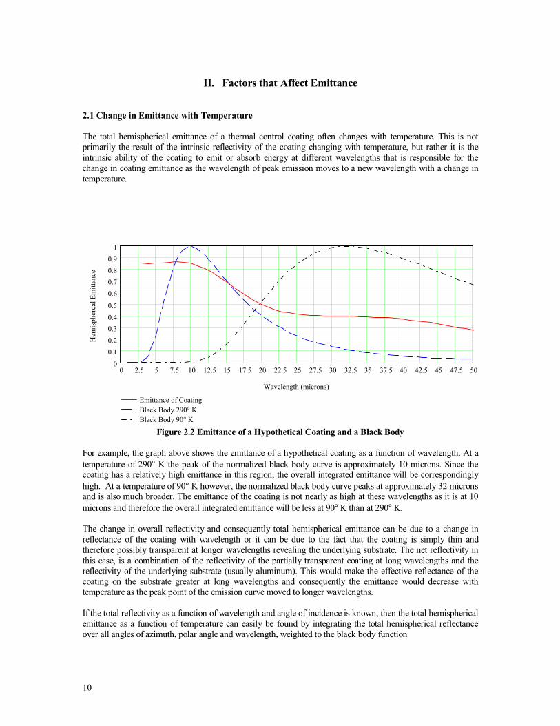
2.1 Change in Emittance with Temperature The total hemispherical emittance of a thermal control coating often changes with temperature. This is not primarily the result of the intrinsic reflectivity of the coating changing with temperature, but rather it is the intrinsic ability of the coating to emit or absorb energy at different wavelengths that is responsible for the change in coating emittance as the wavelength of peak emission moves to a new wavelength with a change in temperature.
Figure 2.2 Emittance of a Hypothetical Coating and a Black Body For example, the graph above shows the emittance of a hypothetical coating as a function of wavelength. At a temperature of 290° K the peak of the normalized black body curve is approximately 10 microns. Since the coating has a relatively high emittance in this region, the overall integrated emittance will be correspondingly high. At a temperature of 90° K however, the normalized black body curve peaks at approximately 32 microns and is also much broader. The emittance of the coating is not nearly as high at these wavelengths as it is at 10 microns and therefore the overall integrated emittance will be less at 90° K than at 290° K. The change in overall reflectivity and consequently total hemispherical emittance can be due to a change in reflectance of the coating with wavelength or it can be due to the fact that the coating is simply thin and therefore possibly transparent at longer wavelengths revealing the underlying substrate. The net reflectivity in this case, is a combination of the reflectivity of the partially transparent coating at long wavelengths and the reflectivity of the underlying substrate (usually aluminum). This would make the effective reflectance of the coating on the substrate greater at long wavelengths and consequently the emittance would decrease with temperature as the peak point of the emission curve moved to longer wavelengths. If the total reflectivity as a function of wavelength and angle of incidence is known, then the total hemispherical emittance as a function of temperature can easily be found by integrating the total hemispherical reflectance over all angles of azimuth, polar angle and wavelength, weighted to the black body function
0 2.5 5 7.5 10 12.5 15 17.5 20 22.5 25 27.5 30 32.5 35 37.5 40 42.5 45 47.5 500
0.10.20.30.40.5
0.60.70.80.9
1
Emittance of CoatingBlack Body 290° KBlack Body 90° K
Wavelength (microns)
Hem
isph
erca
l Em
ittan
ce
11
dTG
dTGdd
= T
∫
∫ ∫ ∫
∞
∞
−
0
0
2
0
2
0
),(
),()cos()sin(),,(1
)(λλ
λλφθθθλφθρ
ε
ππ
(31
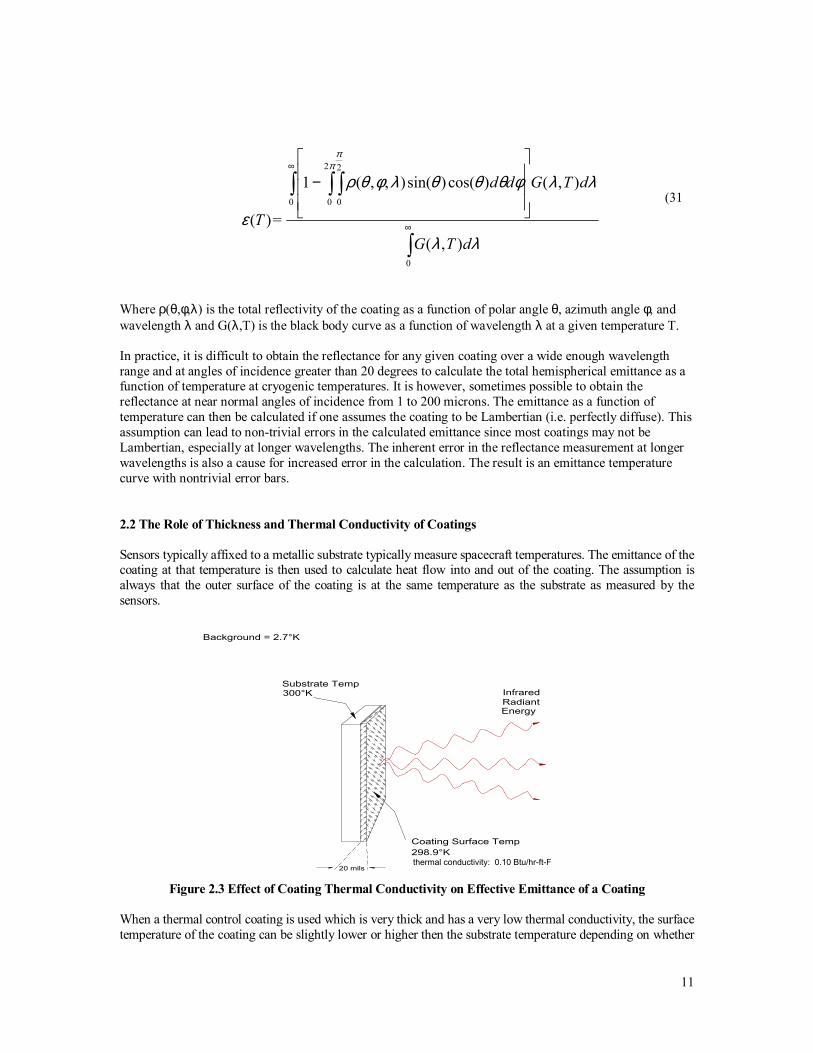
Where ρ(θ,φ,λ) is the total reflectivity of the coating as a function of polar angle θ, azimuth angle φ, and wavelength λ and G(λ,T) is the black body curve as a function of wavelength λ at a given temperature T. In practice, it is difficult to obtain the reflectance for any given coating over a wide enough wavelength range and at angles of incidence greater than 20 degrees to calculate the total hemispherical emittance as a function of temperature at cryogenic temperatures. It is however, sometimes possible to obtain the reflectance at near normal angles of incidence from 1 to 200 microns. The emittance as a function of temperature can then be calculated if one assumes the coating to be Lambertian (i.e. perfectly diffuse). This assumption can lead to non-trivial errors in the calculated emittance since most coatings may not be Lambertian, especially at longer wavelengths. The inherent error in the reflectance measurement at longer wavelengths is also a cause for increased error in the calculation. The result is an emittance temperature curve with nontrivial error bars. 2.2 The Role of Thickness and Thermal Conductivity of Coatings Sensors typically affixed to a metallic substrate typically measure spacecraft temperatures. The emittance of the coating at that temperature is then used to calculate heat flow into and out of the coating. The assumption is always that the outer surface of the coating is at the same temperature as the substrate as measured by the sensors.
Coating Surface Temp
Substrate Temp
Background = 2.7°K
300°K
298.9°K
20 milsthermal conductivity: 0.10 Btu/hr-ft-F
InfraredRadiantEnergy
Figure 2.3 Effect of Coating Thermal Conductivity on Effective Emittance of a Coating
When a thermal control coating is used which is very thick and has a very low thermal conductivity, the surface temperature of the coating can be slightly lower or higher then the substrate temperature depending on whether
12
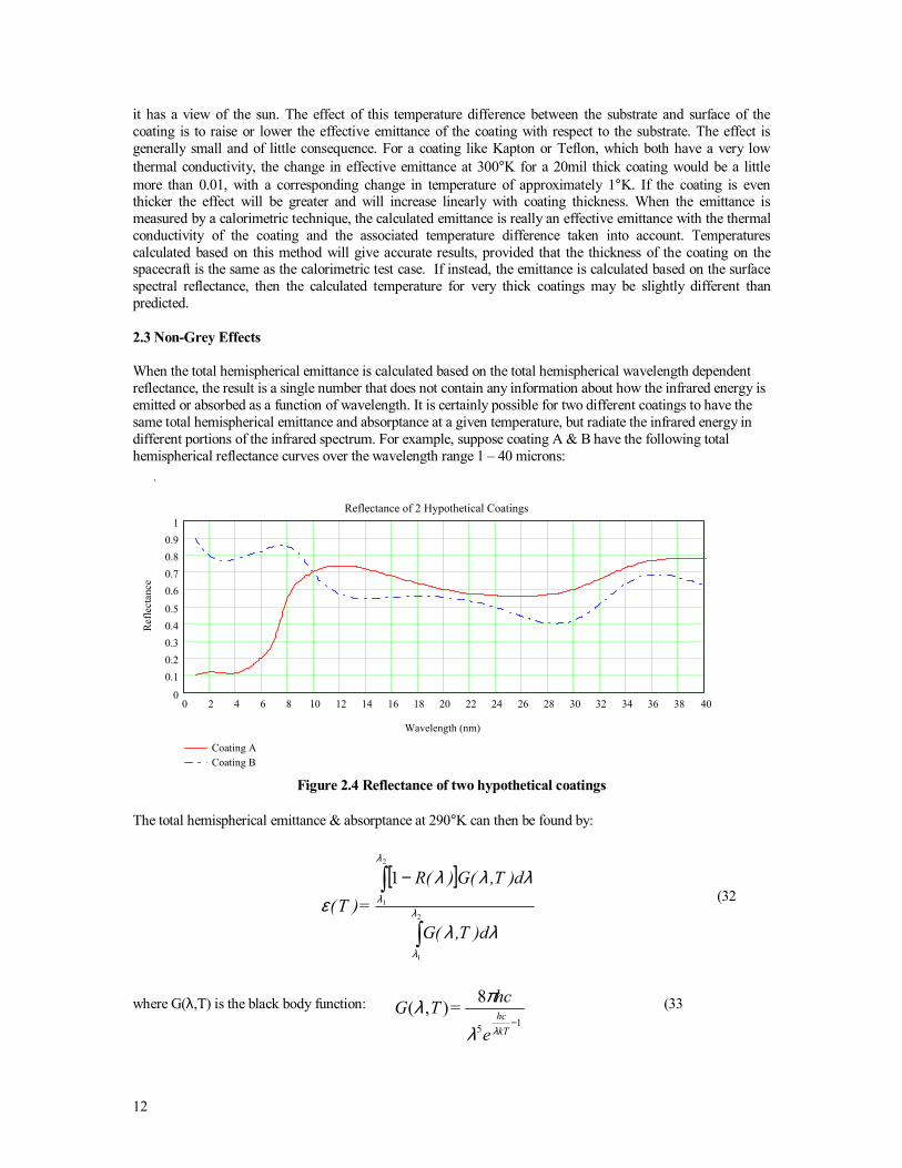
it has a view of the sun. The effect of this temperature difference between the substrate and surface of the coating is to raise or lower the effective emittance of the coating with respect to the substrate. The effect is generally small and of little consequence. For a coating like Kapton or Teflon, which both have a very low thermal conductivity, the change in effective emittance at 300°K for a 20mil thick coating would be a little more than 0.01, with a corresponding change in temperature of approximately 1°K. If the coating is even thicker the effect will be greater and will increase linearly with coating thickness. When the emittance is measured by a calorimetric technique, the calculated emittance is really an effective emittance with the thermal conductivity of the coating and the associated temperature difference taken into account. Temperatures calculated based on this method will give accurate results, provided that the thickness of the coating on the spacecraft is the same as the calorimetric test case. If instead, the emittance is calculated based on the surface spectral reflectance, then the calculated temperature for very thick coatings may be slightly different than predicted. 2.3 Non-Grey Effects When the total hemispherical emittance is calculated based on the total hemispherical wavelength dependent reflectance, the result is a single number that does not contain any information about how the infrared energy is emitted or absorbed as a function of wavelength. It is certainly possible for two different coatings to have the same total hemispherical emittance and absorptance at a given temperature, but radiate the infrared energy in different portions of the infrared spectrum. For example, suppose coating A & B have the following total hemispherical reflectance curves over the wavelength range 1 40 microns:
Figure 2.4 Reflectance of two hypothetical coatings The total hemispherical emittance & absorptance at 290°K can then be found by:
[ ]
d)T,(G
d)T,(G)(R = )T(
∫
∫ −
2
1
2
1
1
λ
λ
λ
λ
λλ
λλλε (32
where G(λ,T) is the black body function: e
hc = TG
kThc 15
8),(−
λλ
πλ (33
.
0 2 4 6 8 10 12 14 16 18 20 22 24 26 28 30 32 34 36 38 400
0.10.20.30.40.5
0.60.70.80.9
1
Coating ACoating B
Reflectance of 2 Hypothetical Coatings
Wavelength (nm)
Ref
lect
ance
13
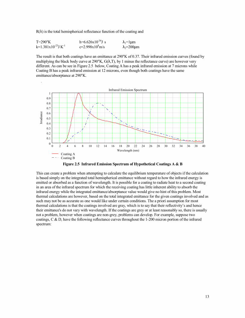
R(λ) is the total hemispherical reflectance function of the coating and T=290°K h=6.626x10⁻³⁴J. s λ1=1µm k=1.381x10⁻²³J K-1 c=2.998x10⁸m/s λ2=200µm The result is that both coatings have an emittance at 290°K of 0.37. Their infrared emission curves (found by multiplying the black body curve at 290°K, G(λ,T), by 1 minus the reflectance curve) are however very different. As can be see in Figure 2.5 below, Coating A has a peak infrared emission at 7 microns while Coating B has a peak infrared emission at 12 microns, even though both coatings have the same emittance/absorptance at 290°K.
.
0 2 4 6 8 10 12 14 16 18 20 22 24 26 28 30 32 34 36 38 400
0.10.20.30.40.5
0.60.70.80.9
1
Coating ACoating B
Infrared Emission Spectrum
Wavelength (nm)
Irra
dian
ce
Figure 2.5 Infrared Emission Spectrum of Hypothetical Coatings A & B
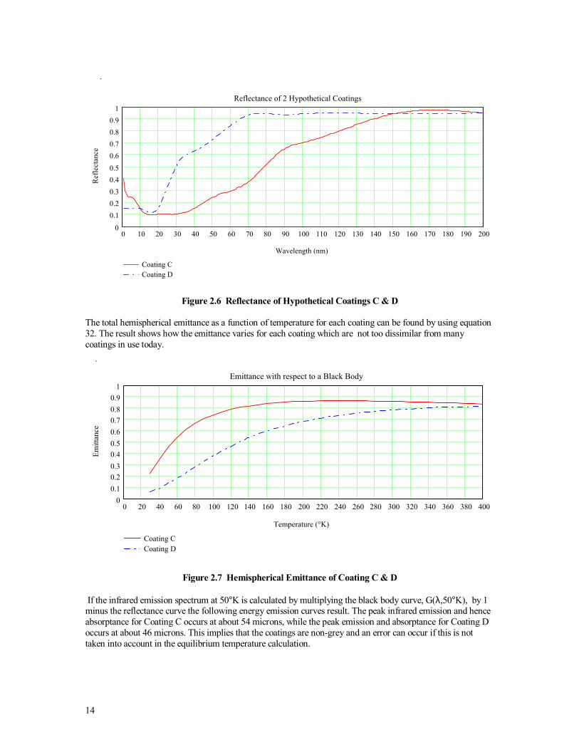
This can create a problem when attempting to calculate the equilibrium temperature of objects if the calculation is based simply on the integrated total hemispherical emittance without regard to how the infrared energy is emitted or absorbed as a function of wavelength. It is possible for a coating to radiate heat to a second coating in an area of the infrared spectrum for which the receiving coating has little inherent ability to absorb the infrared energy while the integrated emittance/absorptance value would give no hint of this problem. Most thermal calculations are however, based on the total integrated emittance for the given coatings involved and as such may not be as accurate as one would like under certain conditions. The a priori assumption for most thermal calculations is that the coatings involved are gray, which is to say that their reflectivitys and hence their emittance's do not vary with wavelength. If the coatings are grey or at least reasonably so, there is usually not a problem, however when coatings are non-grey, problems can develop. For example, suppose two coatings, C & D, have the following reflectance curves throughout the 1-200 micron portion of the infrared spectrum:
14
Figure 2.6 Reflectance of Hypothetical Coatings C & D
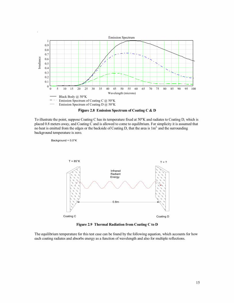
The total hemispherical emittance as a function of temperature for each coating can be found by using equation 32. The result shows how the emittance varies for each coating which are not too dissimilar from many coatings in use today.
Figure 2.7 Hemispherical Emittance of Coating C & D
If the infrared emission spectrum at 50°K is calculated by multiplying the black body curve, G(λ,50°K), by 1 minus the reflectance curve the following energy emission curves result. The peak infrared emission and hence absorptance for Coating C occurs at about 54 microns, while the peak emission and absorptance for Coating D occurs at about 46 microns. This implies that the coatings are non-grey and an error can occur if this is not taken into account in the equilibrium temperature calculation.
.
0 10 20 30 40 50 60 70 80 90 100 110 120 130 140 150 160 170 180 190 2000
0.10.20.30.40.5
0.60.70.80.9
1
Coating CCoating D
Reflectance of 2 Hypothetical Coatings
Wavelength (nm)
Ref
lect
ance
.
0 20 40 60 80 100 120 140 160 180 200 220 240 260 280 300 320 340 360 380 4000
0.10.20.30.40.50.60.70.80.9
1
Coating CCoating D
Emittance with respect to a Black Body
Temperature (°K)
Emitt
ance
15
.
0 5 10 15 20 25 30 35 40 45 50 55 60 65 70 75 80 85 90 95 1000
0.10.20.30.40.50.60.70.80.9
1
Black Body @ 50°KEmission Spectrum of Coating C @ 50°KEmission Spectrum of Coating D @ 50°K
Emission Spectrum
Wavelength (microns)
Irrad
ianc
e
Figure 2.8 Emission Spectrum of Coating C & D
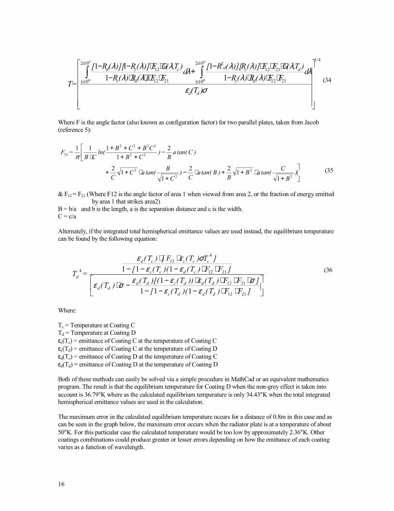
To illustrate the point, suppose Coating C has its temperature fixed at 50°K and radiates to Coating D, which is placed 0.8 meters away, and Coating C and is allowed to come to equilibrium. For simplicity it is assumed that no heat is emitted from the edges or the backside of Coating D, that the area is 1m2, and the surrounding background temperature is zero.
Coating C Coating D
T = 85°K
Background = 0.0°K
T = ?
0.8m
InfraredRadiantEnergy
Figure 2.9 Thermal Radiation from Coating C to D
The equilibrium temperature for this test case can be found by the following equation, which accounts for how each coating radiates and absorbs energy as a function of wavelength and also for multiple reflections.
16
)T(
dFF)(R)(R
)T,(GFF)](R)][(R[dFF)(R)(R
)T,(GF)](R)][(R[
= T
/
dd
x
x dc
dcdx
x dc
ccd
41102
101 2112
21122102
101 2112
12
3
6
3
6 11
111
⋅⋅⋅−⋅⋅⋅−+
⋅⋅⋅⋅−⋅⋅−−
∫∫−
−
−
−
σε
λλλ
λλλλλλ
λλλ(34
Where F is the angle factor (also known as configuration factor) for two parallel plates, taken from Jacob (reference 5):
)Ctan(aB
)CB
CBCBln(CB
= F
−
+++++
⋅2
1111
22
2222
12 π
)B
Ctan(aBB
)Btan(aC
)C
Btan(aCC
+⋅++⋅−
+⋅++
2
2
2
2
1122
112 (35
& F12 = F21 (Where F12 is the angle factor of area 1 when viewed from area 2, or the fraction of energy emitted by area 1 that strikes area2) B = b/a and b is the length, a is the separation distance and c is the width. C = c/a Alternately, if the integrated total hemispherical emittance values are used instead, the equilibrium temperature can be found by the following equation:
]FF)T()(T([]FF)T())T()[(T()T(
]FF)T()(T([]T)T(F[)T(
= T
dddc
dddcdddd
cdcc
ccccd
d
⋅⋅−−−
⋅⋅⋅⋅−−⋅
⋅⋅−−−⋅⋅
2112
2112
2112
412
4
1111
111
εεσεεεσε
εεσεε
(36
Where: Tc = Temperature at Coating C Td = Temperature at Coating D εc(Tc) = emittance of Coating C at the temperature of Coating C εc(Td) = emittance of Coating C at the temperature of Coating D εd(Tc) = emittance of Coating D at the temperature of Coating C εd(Td) = emittance of Coating D at the temperature of Coating D Both of these methods can easily be solved via a simple procedure in MathCad or an equivalent mathematics program. The result is that the equilibrium temperature for Coating D when the non-grey effect is taken into account is 36.79°K where as the calculated equilibrium temperature is only 34.43°K when the total integrated hemispherical emittance values are used in the calculation. The maximum error in the calculated equilibrium temperature occurs for a distance of 0.8m in this case and as can be seen in the graph below, the maximum error occurs when the radiator plate is at a temperature of about 50°K. For this particular case the calculated temperature would be too low by approximately 2.36°K. Other coatings combinations could produce greater or lesser errors depending on how the emittance of each coating varies as a function of wavelength.
17
Figure 2.10 Non-Grey Equilibrium Temperature error for coating C The only way to be sure if a non-grey error is going to present a problem is to measure the total hemispherical reflectance of each of the coatings in question and calculate the temperature based on the reflectance information of each coating over a sufficient wavelength range.
.
0 6 12 18 24 30 36 42 48 54 60 66 72 78 84 90 96 102 108 114 1200
0.5
1
1.5
2
2.5Non-Grey Error
Radiator Plate Temperature (°K)
Erro
r in
Equi
libriu
m T
empe
ratu
re (°
K)
18
III. Measurement of Thermal Properties 3.1 Solar Absorptance
Electromagnetic theory can, at least in principal, be used to calculate the reflectance of a given coating provided the fundamental properties of permittivity, permeability and conductivity are known. In practice however those properties will rarely, if ever, be known for a coating of interest. It is therefore clear that for many purposes the thermal/optical properties of thermal control coatings must be measured in order to know their value to any precision. The calculation of the solar absorptance however, requires knowledge of the total hemispherical reflectance of the coating. This creates special problems in measurement, since the reflected light for many coatings is a composite of both diffuse and specular reflections as is seen in Figure 3.1-1. The incident energy at a given angle, θ, is separated in reflection into a specular component, rs at angle θ and a diffuse component, the rd,s in Figure 3.1-1, which can be at any angle of azimuth β and altitude φ.
β
θ
Incident Enegry
φ
rd
rd
rd
rd
rs
θ
Figure 3.1-1. Directional Total Reflectivity
It is therefore necessary to measure the reflectance by means of an integrating sphere so that both the specular and diffuse components are accounted for or integrated over all angles, β as well as φ to obtain the total hemispherical reflectance for a given angle of incidence. For a given angle of incidence (θ) the absorptance is given by (reference 6):
( ) ( ) ( ) = θτθρθα −−1 (37 Where ρ and τ are the total reflectance and transmittance respectively for a given angle of incidence θ. If the sample is opaque, as is often the case for a thermal control coating, the transmittance is zero and only the total hemispherical reflectance needs to be measured to calculate the total hemispherical absorptance for a given angle of incidence. The total directional solar absorptance can be found from the above equation by weighting the total directional reflectance according to the solar spectrum and integrating over the solar spectrum:
λλ
λλθλθρ
dSdSR
=)(
0
0
)()(),(
∫
∫∞
∞ (38
19
Where S(λ) is the solar extraterrestrial spectrum, and R(λ,θ) is the total directional hemispheric reflectance integrated over all angles of β and φ for a given angle of incidence θ as in Figure 3.1-1. A method and procedure for the measurement of reflectance and calculation of solar absorptance is contained in ASTM E903. This standard gives the procedure for both center sample mounted integrating spheres and side sample mounted integrating spheres, see the Figure 3.1-2 below.
Detector
sample
Reference
Edwards Type Integrating Sphere
Incidence Angle
Reference Beam
Sample Beam
TransmittanceSampleLocation
Reference Beam
Sample BeamSample
Reference
TransmittanceSampleLocation
Detector
Four Port Comparsion Integrating Sphere
Figure 3.1-2. Two Types of Integrating Spheres
The main advantage of a center sample mounted integrating sphere is that the resulting measurement is absolute. The disadvantage is that a small sample, typically about 1 inch in diameter, is required. A side mounted integrating sphere has the advantage that any size sample to within reason can be accounted as long as the sample is flat, but the integrating sphere coating reflectance must be very nearly 100% and uniform over the measurement wavelength because the reflectance does not cancel out of the equations. The center mounted sample sphere has the additional advantage that it will continue to give accurate results even if the sphere coating is degraded, as long as the degradation/contamination is uniform over the entire surface of the sphere. With a side mounted sphere one must always be on guard against sphere degradation/contamination, as measurement errors will result. It is also sometimes useful to know the reflectance of a sample as a function of angle of incidence. The center sample mounted integrating sphere can perform this type of measurement while the side mounted integrating sphere is limited to a near normal angle of incidence. The center-mounted sphere has the advantage that the reflectivity of the sphere coating cancels out of the equations leaving the absolute reflectance of the sample. It also has the advantage that the total hemispherical reflectance can be measured as a function of angle of incidence. The total transmittance of samples can also be measured with the integrating sphere as shown in Figure 3.1-2. This measurement includes not only the direct transmittance but also the scatter transmittance as well and can be used in the calculation of the solar absorptance of transparent films. If it were possible to measure the total hemispheric emittance from zero to infinity then the only error would be the result of the inaccuracy of the reflectance measurement and the error in the solar spectrum data. ASTM E903 states that the typical uncertainty in the calculation of the solar absorptance from the standard solar spectrum and the measured reflectance gives practical error of ± 2%. This however is for reflectance measurements made over the entire wavelength range. In practice however, the integration of the above equation can only be carried out over the wavelength range of the reflectance measurement instrument, which is typically from 250nm to 2800nm. The ASTM E490 indicates that the energy at air mass zero over that wavelength range is only 97.1% of the total solar spectrum, with most of the residual energy being at the infrared portion of the spectrum at wavelengths greater than 2800nm. Therefore, in addition to the inherent
20
±2% error in the calculated solar absorptance as suggested by ASTM E903 there is also a potential error of 2.9% due to the infrared solar energy at wavelengths out of the range of the reflectance instrumentation. So the best solar absorptance that can be calculated is (reference 7 ):
λλλλθλ
θαdS
dSR-1=)(
)()(),(
2800250
2800250
∫
∫ (39
Fortunately, the calculated solar absorptance of many spacecraft thermal control coatings would not be greatly altered if the reflectance beyond 2800nm were actually measured. Reflectance does vary as a function of angle of incidence and this can have an effect on the calculated solar absorptance, but the effect is generally small. The chart below gives the change in calculated solar absorptance as a function of angle of incidence for some common thermal control coatings. Solar absorptances are typically measured at a near normal angle of incidence, typically 10 20 degrees, and unless otherwise stated it should be assumed that the stated solar absorptance value was measured at a near normal angle of incidence.
Angle of
Incidence Solar Absorptance
Z306 OSR Kapton 5mil
A276
10 - 0.050 - - 20 0.952 - 0.43 0.267 30 0.952 - - - 40 0.946 0.441 0.261 45 - 0.049 - - 50 0.941 - - - 60 0.93 0.432 0.250 70 0.903 0.034 - - 80 0.842 - - -
Figure 3.1-3. Solar Absorptance as a Function of Angle of Incidence
The coating thickness can also affect the solar absorptance, particularly white paints. This is primarily due to the fact that most thermal control coatings are rather thin, typically just a few mils thick and hence tend to be semi-transparent when applied thinner than recommended. The chart below shows how solar absorptance can vary for a white silicone coating as a function of coating thickness.
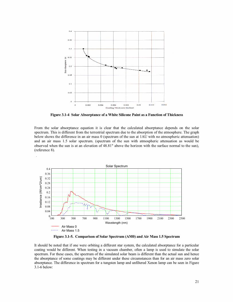
21
Figure 3.1-4 Solar Absorptance of a White Silicone Paint as a Function of Thickness
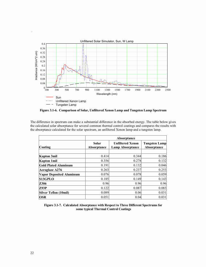
From the solar absorptance equation it is clear that the calculated absorptance depends on the solar spectrum. This is different from the terrestrial spectrum due to the absorption of the atmosphere. The graph below shows the difference in an air mass 0 (spectrum of the sun at 1AU with no atmospheric attenuation) and an air mass 1.5 solar spectrum. (spectrum of the sun with atmospheric attenuation as would be observed when the sun is at an elevation of 48.81° above the horizon with the surface normal to the sun), (reference 8).
Figure 3.1-5. Comparison of Solar Spectrum (AM0) and Air Mass 1.5 Spectrum
It should be noted that if one were orbiting a different star system, the calculated absorptance for a particular coating would be different. When testing in a vacuum chamber, often a lamp is used to simulate the solar spectrum. For these cases, the spectrum of the simulated solar beam is different than the actual sun and hence the absorptance of some coatings may be different under these circumstances than for an air mass zero solar absorptance. The difference in spectrum for a tungsten lamp and unfiltered Xenon lamp can be seen in Figure 3.1-6 below:
.
100 300 500 700 900 1100 1300 1500 1700 1900 2100 2300 25000
0.040.080.120.16
0.20.240.280.320.36
0.4
Air Mass 0Air Mass 1.5
Solar Spectrum
Wavelength (nm)
Irrad
ianc
e (W
/cm
^2/u
m)
22
Figure 3.1-6. Comparison of Solar, Unfiltered Xenon Lamp and Tungsten Lamp Spectrum The difference in spectrum can make a substantial difference in the absorbed energy. The table below gives the calculated solar absorptance for several common thermal control coatings and compares the results with the absorptance calculated for the solar spectrum, an unfiltered Xenon lamp and a tungsten lamp.
Absorptance
Coating Solar
Absorptance Unfiltered Xenon Lamp Absorptance
Tungsten Lamp Absorptance
Kapton 3mil 0.414 0.344 0.186Kapton 1mil 0.356 0.278 0.132Gold Plated Aluminum 0.191 0.132 0.046Aeroglaze A276 0.263 0.237 0.253Vapor Deposited Aluminum 0.076 0.078 0.059S13GPLO 0.185 0.149 0.143Z306 0.96 0.96 0.96Z93P 0.122 0.087 0.083Silver Teflon (10mil) 0.089 0.06 0.031OSR 0.051 0.04 0.031
Figure 3.1-7. Calculated Absorptance with Respect to Three Different Spectrums for
some typical Thermal Control Coatings
.
100 300 500 700 900 1100 1300 1500 1700 1900 2100 2300 25000
0.040.080.120.16
0.20.240.280.320.36
0.4
SunUnfiltered Xenon LampTungsten Lamp
Unfiltered Solar Simulator, Sun, W Lamp
Wavelength (nm)
Irrad
ianc
e (W
/cm
^2 u
m)
.
23
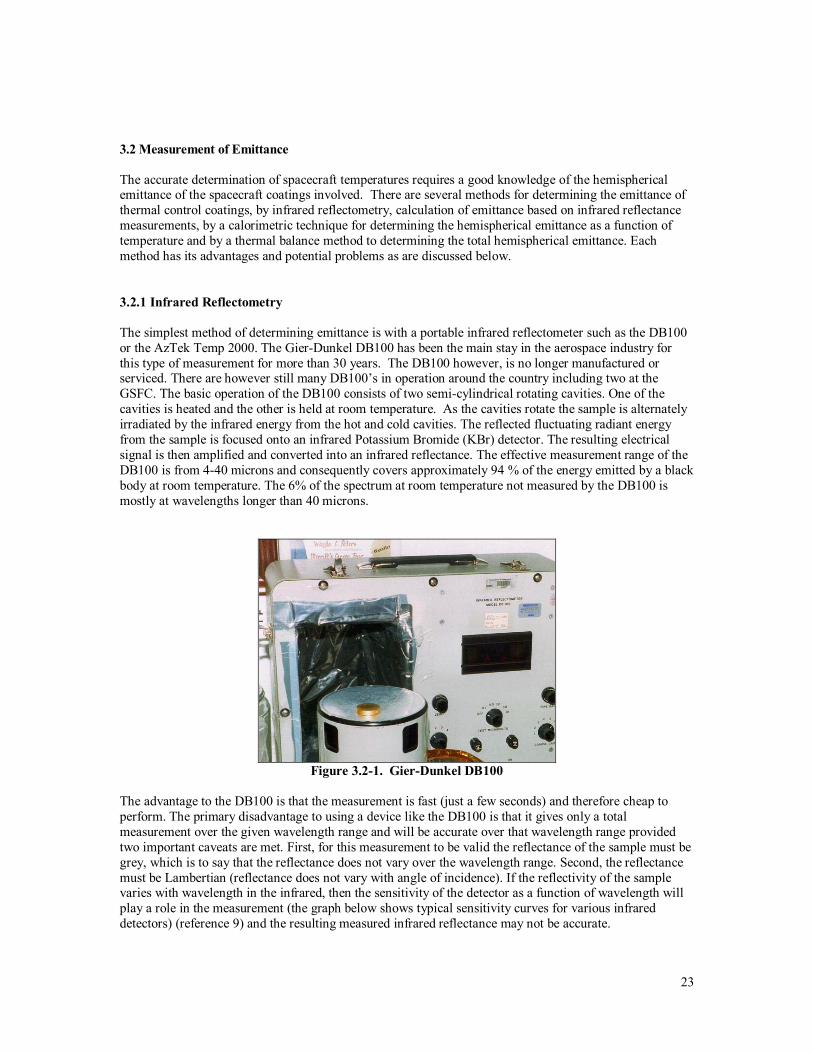
3.2 Measurement of Emittance The accurate determination of spacecraft temperatures requires a good knowledge of the hemispherical emittance of the spacecraft coatings involved. There are several methods for determining the emittance of thermal control coatings, by infrared reflectometry, calculation of emittance based on infrared reflectance measurements, by a calorimetric technique for determining the hemispherical emittance as a function of temperature and by a thermal balance method to determining the total hemispherical emittance. Each method has its advantages and potential problems as are discussed below. 3.2.1 Infrared Reflectometry The simplest method of determining emittance is with a portable infrared reflectometer such as the DB100 or the AzTek Temp 2000. The Gier-Dunkel DB100 has been the main stay in the aerospace industry for this type of measurement for more than 30 years. The DB100 however, is no longer manufactured or serviced. There are however still many DB100s in operation around the country including two at the GSFC. The basic operation of the DB100 consists of two semi-cylindrical rotating cavities. One of the cavities is heated and the other is held at room temperature. As the cavities rotate the sample is alternately irradiated by the infrared energy from the hot and cold cavities. The reflected fluctuating radiant energy from the sample is focused onto an infrared Potassium Bromide (KBr) detector. The resulting electrical signal is then amplified and converted into an infrared reflectance. The effective measurement range of the DB100 is from 4-40 microns and consequently covers approximately 94 % of the energy emitted by a black body at room temperature. The 6% of the spectrum at room temperature not measured by the DB100 is mostly at wavelengths longer than 40 microns.
Figure 3.2-1. Gier-Dunkel DB100
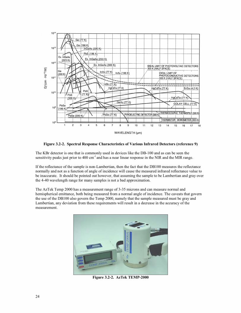
The advantage to the DB100 is that the measurement is fast (just a few seconds) and therefore cheap to perform. The primary disadvantage to using a device like the DB100 is that it gives only a total measurement over the given wavelength range and will be accurate over that wavelength range provided two important caveats are met. First, for this measurement to be valid the reflectance of the sample must be grey, which is to say that the reflectance does not vary over the wavelength range. Second, the reflectance must be Lambertian (reflectance does not vary with angle of incidence). If the reflectivity of the sample varies with wavelength in the infrared, then the sensitivity of the detector as a function of wavelength will play a role in the measurement (the graph below shows typical sensitivity curves for various infrared detectors) (reference 9) and the resulting measured infrared reflectance may not be accurate.
24
Figure 3.2-2. Spectral Response Characteristics of Various Infrared Detectors (reference 9)
The KBr detector is one that is commonly used in devices like the DB-100 and as can be seen the sensitivity peaks just prior to 400 cm-1 and has a near linear response in the NIR and the MIR range. If the reflectance of the sample is non-Lambertian, then the fact that the DB100 measures the reflectance normally and not as a function of angle of incidence will cause the measured infrared reflectance value to be inaccurate. It should be pointed out however, that assuming the sample to be Lambertian and gray over the 4-40 wavelength range for many samples is not a bad approximation. The AzTek Temp 2000 has a measurement range of 3-35 microns and can measure normal and hemispherical emittance, both being measured from a normal angle of incidence. The caveats that govern the use of the DB100 also govern the Temp 2000, namely that the sample measured must be gray and Lambertian, any deviation from these requirements will result in a decrease in the accuracy of the measurement.
Figure 3.2-2. AzTek TEMP-2000
25
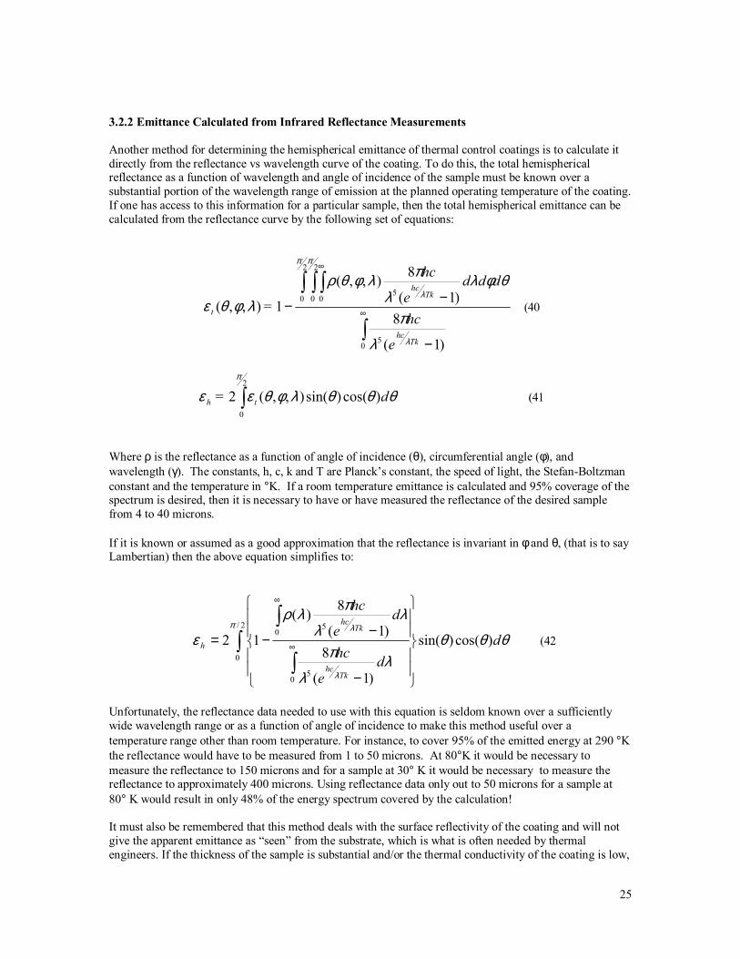
3.2.2 Emittance Calculated from Infrared Reflectance Measurements Another method for determining the hemispherical emittance of thermal control coatings is to calculate it directly from the reflectance vs wavelength curve of the coating. To do this, the total hemispherical reflectance as a function of wavelength and angle of incidence of the sample must be known over a substantial portion of the wavelength range of emission at the planned operating temperature of the coating. If one has access to this information for a particular sample, then the total hemispherical emittance can be calculated from the reflectance curve by the following set of equations:
∫
∫ ∫ ∫∞
∞
−
−−
05
2
0
2
0 05
)1(
8)1(
8),,(
1),,(
Tkhc
Tkhc
t
e
hc
ddde
hc
=
λ
π π
λ
λ
π
θφλλ
πλφθρ
λφθε (40
∫2
0
)cos()sin(),,(2π
θθθλφθεε d= th (41
Where ρ is the reflectance as a function of angle of incidence (θ), circumferential angle (φ), and wavelength (γ). The constants, h, c, k and T are Plancks constant, the speed of light, the Stefan-Boltzman constant and the temperature in °K. If a room temperature emittance is calculated and 95% coverage of the spectrum is desired, then it is necessary to have or have measured the reflectance of the desired sample from 4 to 40 microns. If it is known or assumed as a good approximation that the reflectance is invariant in φ and θ, (that is to say Lambertian) then the above equation simplifies to:
θθθλ
λ
π
λλ
πλρ
επ
λ
λd
de
hc
de
hc
Tkhc
Tkhc
h )cos()sin(
)1(
8)1(
8)(
122/
0
05
05
∫∫
∫
−
−−= ∞
∞
(42
Unfortunately, the reflectance data needed to use with this equation is seldom known over a sufficiently wide wavelength range or as a function of angle of incidence to make this method useful over a temperature range other than room temperature. For instance, to cover 95% of the emitted energy at 290 °K the reflectance would have to be measured from 1 to 50 microns. At 80°K it would be necessary to measure the reflectance to 150 microns and for a sample at 30° K it would be necessary to measure the reflectance to approximately 400 microns. Using reflectance data only out to 50 microns for a sample at 80° K would result in only 48% of the energy spectrum covered by the calculation! It must also be remembered that this method deals with the surface reflectivity of the coating and will not give the apparent emittance as seen from the substrate, which is what is often needed by thermal engineers. If the thickness of the sample is substantial and/or the thermal conductivity of the coating is low,
26
then the surface temperature of the coating can be substantially different from the substrate and hence the coating will appear to have a lower emittance with respect to the substrate than has been calculated by the above method. 3.2.3 Calorimetric Technique for Determining Hemispherical Emittance The transient calorimetric technique is an accurate but also the most time consuming method of determining total hemispherical emittance as a function of temperature. The technique relies on accurately timing the cool down rate of a block of known specific heat capacity (usually pure aluminum) coated with the material (usually a paint or thin film). Then from knowledge of the specific heat, total area of the sample and cool down rate, the emittance can be calculated. In practice, parasitic heat losses can affect the accuracy of the measurement at cryogenic temperatures and therefore must be minimized or eliminated from the test and taken into account during the calculation. The parasitic heat losses/inputs primarily arise from the heat lost due to the residual gas in the vacuum chamber, heat conducted through and emitted from the temperature sensor leads, heat from the sample being reflected back to the sample from the chamber walls, radiant heat from the outside striking the sample, or heat dissipated by the temperature sensor into the sample substrate. In this test method it is assumed that the specific heat of the coating itself is small with respect to the aluminum substrate. If this is not true, then the specific heat as a function of temperature must be known for the coating in order for an accurate calculation of the emittance of the coating to be made. The transient calorimetric technique typically consists of a pure Aluminum block (or A1100 Aluminum as a good substitute) coated with a typical spacecraft coating and suspended via the manganin temperature sensor leads in a black painted liquid helium shroud. During testing, the specimen is first heated to 340°K by solar simulator beam input through Infrasil windows. This starting temperature will not only give values for emittance slightly above room temperature, which are sometimes desired, but also allow the room temperature value to checked by a DB100 or similar such device. Then the input port is covered and the specimen allowed to cool by radiation to the liquid helium shroud in a vacuum of better than 10-6 torr. Under the conditions present in the chamber the heat-balance equation is given by:
QsdQgasQlltTCpm
tTmCp=TsaTsTaT ss −−−
∆∆−
∆∆−− 44 )()( σεσε (43
Where ε(T), a, σ, T, Ts, m, Cp, ∆T/∆t, ms, Cps are the emittance of the sample at a given temperature, sample area, the Stefan-Boltzman constant , sample temperature, shroud temperature, sample mass, specific heat of aluminum, sample cooling rate, mass of the sample coating, specific heat of the sample coating respectively. If the total area of the sample is small with respect to the total area of the chamber, the heat emitted from the sample and subsequently reflected from the chamber wall back to the sample can be neglected. The Qsd term represents the heat supplied to the aluminum block by the silicon diode temperature sensor. This amounts to a few micron watts and represents only a minor correction factor even at 40°K. Qll represents the heat loss due to conduction and radiation of heat down the manganin wires and Qgas is the heat loss due to the conduction of heat by the residual gas in the chamber. This method works well as long as the thermal mass of the coating is small with respect to the substrate used and as long as the specific heat of the substrate is known over the entire temperature range of interest to a high degree of accuracy. For this reason it is advantageous to use A1100 Aluminum since its specific heat as a function of temperature is well known. Also, the sample area must be small with respect to the area of the shroud in order to minimize the reflection of heat from the sample back to the sample. The pressure in the chamber must also be kept as low as possible to minimize the conduction of heat from the sample to the shroud wall by residual gasses in the chamber. The actual operating pressure of course depends on the temperature range of interest. For a lower temperature range of 150°C a pressure of 1x10⁻⁶
27
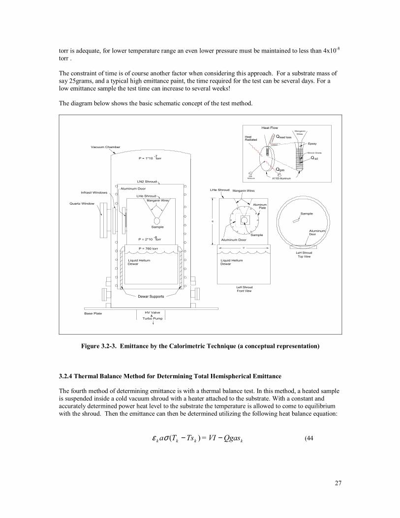
torr is adequate, for lower temperature range an even lower pressure must be maintained to less than 4x10⁻⁸ torr . The constraint of time is of course another factor when considering this approach. For a substrate mass of say 25grams, and a typical high emittance paint, the time required for the test can be several days. For a low emittance sample the test time can increase to several weeks! The diagram below shows the basic schematic concept of the test method.
Liquid Helium
LN2 Shroud
Quartz Window
Infrasil Windows
Vacuum Chamber
LHe Shroud
Sample
Manganin Wires
Q
Q
Heat Flow
GasMolecule
Liquid Helium
LHe Shroud
Sample
Manganin Wires
Aluminum Door
P = 760 torr
P = 1*10 torr-7
P = 2*10 torr-8
Aluminum Door
Base Plate HV Valve
Turbo Pump
AluminumPlate
radiated
cond
u cte
d
Q
&
Front View
Top View
AluminumDoor
Sample
Dewar Dewar
Silicon Diode
ManganinWires
Dewar Supports
A1100 Aluminum
Epoxy
gas
sd
lead lossHeatRadiated
LeH Shroud
LeH Shroud
Figure 3.2-3. Emittance by the Calorimetric Technique (a conceptual representation)
3.2.4 Thermal Balance Method for Determining Total Hemispherical Emittance The fourth method of determining emittance is with a thermal balance test. In this method, a heated sample is suspended inside a cold vacuum shroud with a heater attached to the substrate. With a constant and accurately determined power heat level to the substrate the temperature is allowed to come to equilibrium with the shroud. Then the emittance can then be determined utilizing the following heat balance equation: kkkk QgasVI=TsTa −− )(σε (44
28
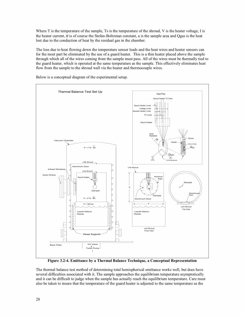
Where T is the temperature of the sample, Ts is the temperature of the shroud, V is the heater voltage, I is the heater current, σ is of course the Stefan-Boltzman constant, a is the sample area and Qgas is the heat lost due to the conduction of heat by the residual gas in the chamber. The loss due to heat flowing down the temperature sensor leads and the heat wires and heater sensors can for the most part be eliminated by the use of a guard heater. This is a thin heater placed above the sample through which all of the wires coming from the sample must pass. All of the wires must be thermally tied to the guard heater, which is operated at the same temperature as the sample. This effectively eliminates heat flow from the sample to the shroud wall via the heater and thermocouple wires. Below is a conceptual diagram of the experimental setup.
Liquid Helium
LN2 Shroud
Quartz Window
Infrasil Windows
Vacuum Chamber
LHe Shroud
Sample
Thermal Balance Test Set Up
Q
Heat Flow
GasMolecule
P = 760 torr
P = 1*10 torr-7
P = 2*10 torr-8
Aluminum Door
Base Plate HV Valve
Turbo Pump
Q
&
Dewar
Silicon Diode
Dewar Supports
A1100 Aluminum
Epoxy
gas
sd
HeatRadiated
Liquid Helium
LHe Shroud
Sample
Aluminum Door
AluminumPlate
Front View
Top View
AluminumDoor
Sample
Dewar
LeH Shroud
LeH Shroud
Gaurd Heater
Sample Heater Lines
TC Lines
Gaurd Heater TC lines
Volatge Lines
Gaurd Heater Lines
QrHeater
Gaurd Heater
Figure 3.2-4. Emittance by a Thermal Balance Technique, a Conceptual Representation The thermal balance test method of determining total hemispherical emittance works well, but does have several difficulties associated with it. The sample approaches the equilibrium temperature asymptotically and it can be difficult to judge when the sample has actually reach the equilibrium temperature. Care must also be taken to insure that the temperature of the guard heater is adjusted to the same temperature as the
29
sample. Adjusting the guard heater temperature can however, affect the sample temperature and this further complicates the judgement of the equilibrium temperature. The guard heater itself must be constructed in such a way that all the wires passing through it, the heater wires, the thermocouple wires and voltage measurement wires, are in good thermal contact with the heater over the test temperature range. This can be a problem if the wires are of different diameter, or have different insulation thicknesses. Lastly, a low emittance coating should be applied to the wire insulation between the sample and the guard heater to minimize the heat radiated to the shroud wall by the wire insulation. 3.2.5 Methods of Increasing Emittance A high thermal emittance is typically desired for many applications. Achieving a sufficiently high emittance can be a difficult thing to achieve. The typical methods for achieving a high emittance include roughening the surface, increasing the thickness of the coating, and the use of coated honeycomb material. Each has its limitations. In the first case, increasing the thickness of the coating will increase the emittance, but only up to a maximum value. Beyond a material specific thickness, applying a thicker coating will actually lower the effective emittance. This occurs when the thermal conductivity of the coating is low enough to allow the surface temperature of the coating to fall below the substrate temperature. This will in turn lower the amount of heat radiated to space and consequently the material will appear to have a lower emittance and in fact the effective emittance of the coating will drop. It is in some respects akin to putting a thermal blanket (MLI) over the substrate; although the true emittance of the surface hasnt changed the effective emittance of the coating will appear low and the total heat rejected to space as a consequence will be lower. Honeycomb works well at increasing the effective emittance of a coating. It must be kept in mind however that the typical cells in a honeycomb sheet are small and numerous. Their small size and number makes abrading the surface in preparation for painting impossible. This means that cleaning the cells is the only method of ensuring good adhesion of the paint to the cell wall. It must be also kept in mind that the cells are concave and therefore any adhesion problem will be exasperated by the concave nature of the honeycomb cells. This will be especially true at cryogenic temperature, where the CTE mismatch between the coating and the honeycomb aluminum combined with the concave nature of the cells can make adhesion difficult. Any loss of adhesion will of course result in a drop in effective emittance of the honeycomb cell. 3.2.6 Considerations and Lessons Learned When considering emittance there are some important points to keep in mind with spacecraft coatings. First is that coatings are typically thin and since emittance depends to some extent on the thickness of the coating it is important to be sure that the coating has the specified thickness. If your coating is thinner than is typical or specified, the emittance for that coating may not be valid. Also, since some coatings are partially transparent, the emittance to some extent depends on the given substrate. Typically emittances are measured over aluminum since this is the most common spacecraft substrate. If the substrate is other than a metal, then emittance of the coating could be different than expected, especially if the coating is thinner than is typical. It should also be remembered that some paints have several different primers that can be used and the use of a different primer or the lack of a primer can affect the emittance. In conclusion, the thickness and emittance of the coating should always be checked after the coating is applied.
30
3.3 Electrical Properties During space flight missions spacecraft can encounter energetic charged particles that can cause differential charging of the spacecraft. This differential charging can result in electrostatic discharges (ESD) between various parts of the spacecraft. This ESD is a source of electromagnetic interference (EMI) which can be coupled to electronic devices. Sensitive ICs can be damaged by several mJ (milli-Joule) of ESD and circuits can be upset with only several nJ (nano-Joule). This charging phenomenon has been blamed for arcing that has caused blown fuses and loss of data transmission on several spacecraft. ESD can also cause electronic parts failure, operational anomalies, degradation of thermal control surfaces, and can also render low energy particle detectors useless. The principal cause of spacecraft charging is the charged particles trapped by the earths magnetic field. The differential charging of the relatively thin spacecraft thermal control coatings is due primarily to the low energy charged particles in the Van Allen radiation belts. The penetration depth of the high-energy charged particles is greater than the typical thermal control coatings and therefore these do not contribute much to the surface charging of the coatings. The Van Allen belts, which are responsible for most spacecraft charging, are sometimes modified by magnetic disturbances and the solar cycle but generally exist from approximately 1000 km to 6 Earth radii. In low Earth orbit ( below 1000km) spacecraft charging is not much of a concern. The Van Allen belts are generally symmetric in azimuth about the geomagnetic equator and extends to ± 50 degrees above and below it (reference 11 & 12). The actual flux and energy encountered needs to be calculated for each mission based on the spacecraft orbit and time of launch with respect to the solar cycle. The charts below (reference 13) show typical distributions of trapped electrons and protons of varying energies and earth radii
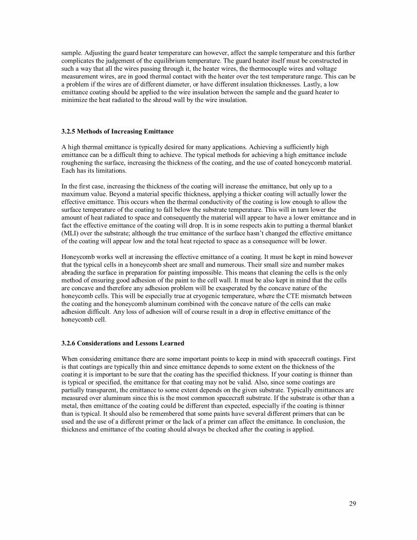
Figure 3.3.1 (A) Distribution of trapped electrons Figure 3.3.2 (A), Distribution of trapped During solar minimum with energy greater than protons with energy greater than 1 MeV. 0.5 MeV. (B) Distribution of electrons with same (B), Distribution of trapped protons with energy during solar maximun. (reference 13) energy greater than 100 MeV (reference 13)
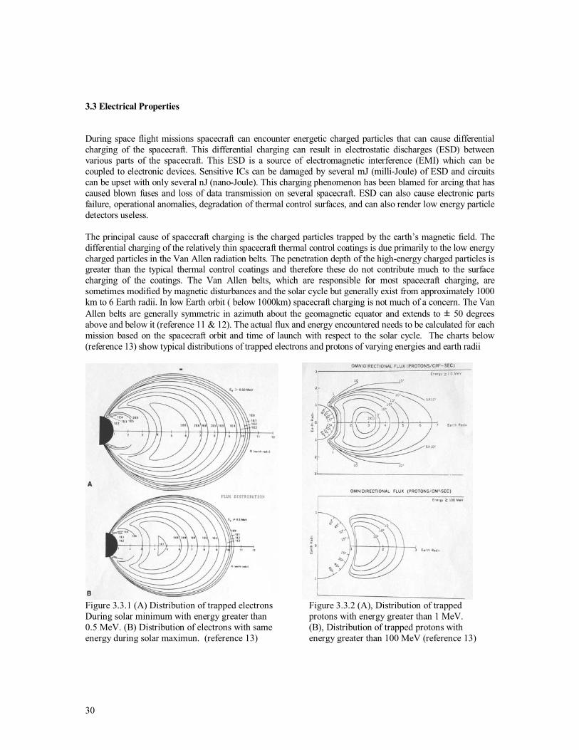
31
- Figure 3.3.3 The radiation due to trapped protons in Figure 3.3.4 The radiation due to trapped electrons a 400 km polar orbit and in a 500 km, 57° inclination encountered in a 400 km polar orbit and in a 500 km orbit. (reference 13) (reference 13) Differential spacecraft charging is determined by a number of factors such as photo emission from the coating, temperature of the coating, secondary emission of electrons, contamination of the surface, intensity of radiation, and type of coating. Differential spacecraft charging is primarily the result of low energy electron flux. High-energy electrons penetrate the thin thermal coatings and therefore do not contribute to the differential charging process. Low energy protons do not penetrate the coatings and therefore they tend to lessen the charging caused by the electrons, but they do not eliminate it. This is because proton flux is much less than the electron flux. This may seem paradoxical since space is on the whole charge neutral. The reason the electron flux is greater is not due to the fact that there are more electrons in space than protons. Thermodynamics requires that the electrons and protons be in thermodynamic equilibrium with each other. Since the mass of the electrons is so much less than the mass of protons they must travel faster than the protons in order to reach the same kinetic energy and hence thermal equilibrium. This means that the total number of electrons passing a given point in a fixed amount of time is greater than protons. So the spacecraft receives a much grater electron flux than proton flux. NASA's preferred reliability practices manual (reference 14) recommends that the energy stored by each nonconductive surface be less than 3mJ, and that ESD (electrostatic discharges) should not be allowed to occur near receivers or antennas operating at less than 8GHz or near sensitive circuits. This implies that the spacecraft must be immune to 3mJ ESD. NASA's NASCAP program will calculate the maximum differential charging on each non-conducting surface if the conductivity of the coatings is known. The electric field strength within a spacecraft coating can be calculated if the coating thickness and surface voltage are known and is given by:
dV=E / (45 Where d is the thickness of the dielectric material. Usually when this electric field strength is greater than 2x10⁵V/cm the risk of ESD is present.
32
The total ESD energy can be calculated from:
CV
=W 221
(46
Where C is the capacitance of the nonconductive surface with respect to spacecraft ground.
d
A =C coεε
(47
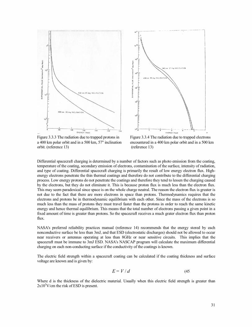
where d= the thickness of the coating and εc is the permittivity of the coating and A is the total area of the coating. To calculate the total energy on each surface of the spacecraft the charge voltage must be known. This too can be calculated if the resistivities of the coatings are known as well as the total charge current impinging on the coating in space. If the resistance is not known, ground-based test must be conducted to determine these parameters. The ESD energy as a function of capacitance and voltage level is displayed in the following diagram taken from NASA's preferred reliability manual:
Figure 3.3-1. ESD Energy as a Function of Capacitance and Voltage
Since the current available in the space environment is relatively low, material with a resistivity of 109 Ohm-cm are usually considered adequate for effective charge control. For some missions however it is not unusual for a requirement of not more then 1-volt potential difference to exist between any two parts of the spacecraft. This is far below the 3mJ limit of acceptability to prevent ESD. Under these stringent requirements a more conductive coating is necessary. When spacecraft charging is of concern two basic cases must be considered in order to measure the conductivity or predict the charging level. The first case deals with a conductive coating on a nonconductive substrate. In this situation charge control is achieved through the inherent sheet conductivity of the coating.
33
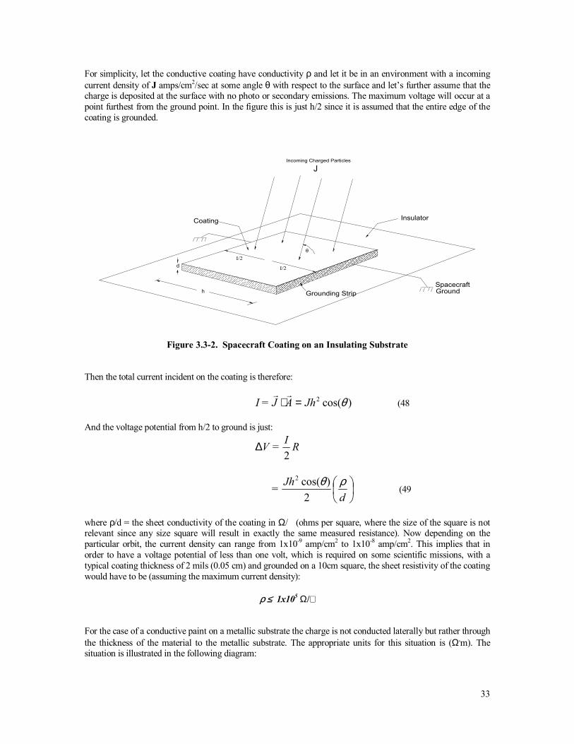
For simplicity, let the conductive coating have conductivity ρ and let it be in an environment with a incoming current density of J amps/cm2/sec at some angle θ with respect to the surface and lets further assume that the charge is deposited at the surface with no photo or secondary emissions. The maximum voltage will occur at a point furthest from the ground point. In the figure this is just h/2 since it is assumed that the entire edge of the coating is grounded.
h
dI/2
I/2
J
θ
Insulator
Grounding StripSpacecraftGround
Coating
Incoming Charged Particles
Figure 3.3-2. Spacecraft Coating on an Insulating Substrate
Then the total current incident on the coating is therefore:
)cos(2 θJhAJ = I =⋅rr
(48 And the voltage potential from h/2 to ground is just:
RI=V2
∆
dJh= ρθ
2)cos(2
(49
where ρ/d = the sheet conductivity of the coating in Ω/ (ohms per square, where the size of the square is not relevant since any size square will result in exactly the same measured resistance). Now depending on the particular orbit, the current density can range from 1x10⁻⁹ amp/cm2 to 1x10⁻⁸ amp/cm2. This implies that in order to have a voltage potential of less than one volt, which is required on some scientific missions, with a typical coating thickness of 2 mils (0.05 cm) and grounded on a 10cm square, the sheet resistivity of the coating would have to be (assuming the maximum current density):
ρ ≤ 1x10⁵ Ω/ For the case of a conductive paint on a metallic substrate the charge is not conducted laterally but rather through the thickness of the material to the metallic substrate. The appropriate units for this situation is (Ω.m). The situation is illustrated in the following diagram:
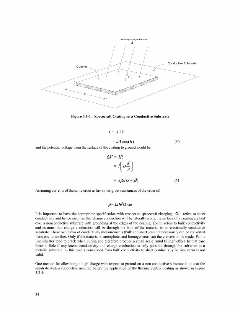
34
h
d
J
θ
Conductive SubstrateCoating
Incoming Charged Particles
Figure 3.3-3. Spacecraft Coating on a Conductive Substrate
AJ=Irr
⋅ )cos(θJA= (50 and the potential voltage from the surface of the coating to ground would be:
IR=V∆
AdI= ρ
)cos(θρdJ= (51
Assuming currents of the same order as last times gives resistances of the order of:
ρ = 2x10⁹Ω-cm
It is important to have the appropriate specification with respect to spacecraft charging, Ω/ refers to sheet conductivity and hence assumes that charge conduction will be laterally along the surface of a coating applied over a nonconductive substrate with grounding at the edges of the coating. Ω-cm refers to bulk conductivity and assumes that charge conduction will be through the bulk of the material to an electrically conductive substrate. These two forms of conductivity measurements (bulk and sheet) can not necessarily can be converted from one to another. Only if the material is amorphous and homogeneous can the conversion be made. Paints like silicates tend to crack when curing and therefore produce a small scale mud tilling effect. In that case there is little if any lateral conductivity and charge conduction is only possible through the substrate to a metallic substrate. In this case a conversion from bulk conductivity to sheet conductivity or vice versa is not valid. One method for alleviating a high charge with respect to ground on a non-conductive substrate is to coat the substrate with a conductive medium before the application of the thermal control coating as shown in Figure 3.3-4:
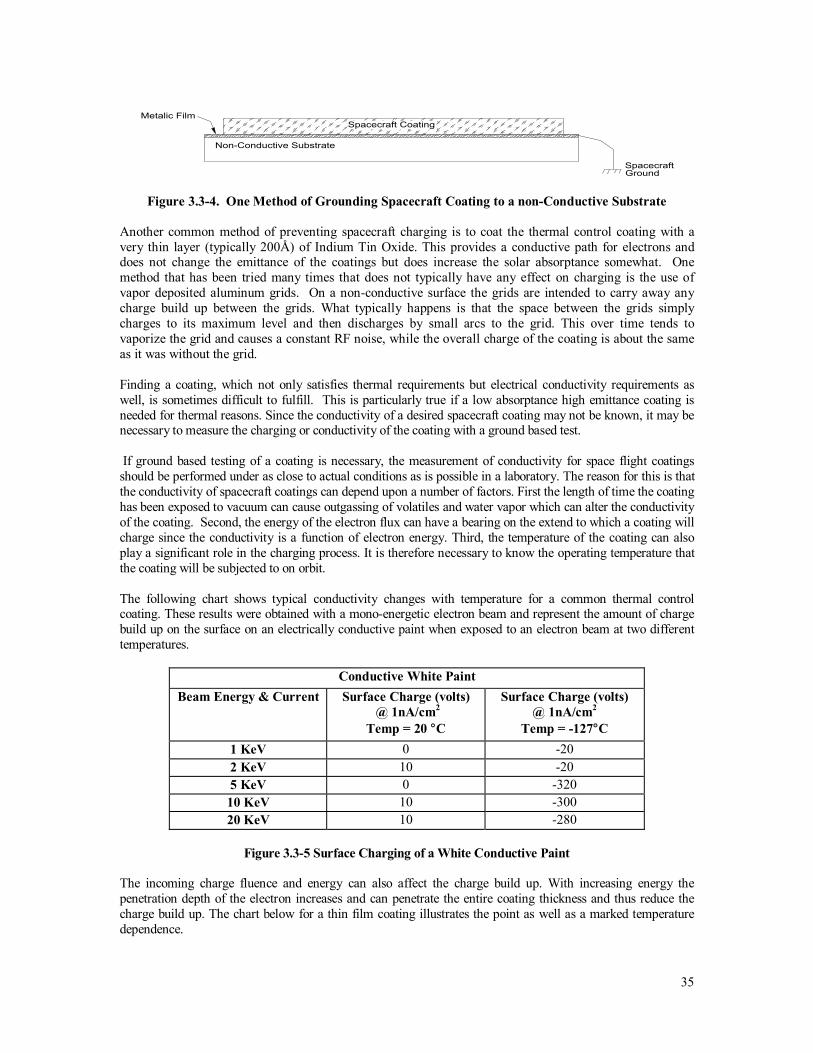
35
Metalic FilmSpacecraft Coating
Non-Conductive Substrate
SpacecraftGround
Figure 3.3-4. One Method of Grounding Spacecraft Coating to a non-Conductive Substrate
Another common method of preventing spacecraft charging is to coat the thermal control coating with a very thin layer (typically 200Å) of Indium Tin Oxide. This provides a conductive path for electrons and does not change the emittance of the coatings but does increase the solar absorptance somewhat. One method that has been tried many times that does not typically have any effect on charging is the use of vapor deposited aluminum grids. On a non-conductive surface the grids are intended to carry away any charge build up between the grids. What typically happens is that the space between the grids simply charges to its maximum level and then discharges by small arcs to the grid. This over time tends to vaporize the grid and causes a constant RF noise, while the overall charge of the coating is about the same as it was without the grid. Finding a coating, which not only satisfies thermal requirements but electrical conductivity requirements as well, is sometimes difficult to fulfill. This is particularly true if a low absorptance high emittance coating is needed for thermal reasons. Since the conductivity of a desired spacecraft coating may not be known, it may be necessary to measure the charging or conductivity of the coating with a ground based test. If ground based testing of a coating is necessary, the measurement of conductivity for space flight coatings should be performed under as close to actual conditions as is possible in a laboratory. The reason for this is that the conductivity of spacecraft coatings can depend upon a number of factors. First the length of time the coating has been exposed to vacuum can cause outgassing of volatiles and water vapor which can alter the conductivity of the coating. Second, the energy of the electron flux can have a bearing on the extend to which a coating will charge since the conductivity is a function of electron energy. Third, the temperature of the coating can also play a significant role in the charging process. It is therefore necessary to know the operating temperature that the coating will be subjected to on orbit. The following chart shows typical conductivity changes with temperature for a common thermal control coating. These results were obtained with a mono-energetic electron beam and represent the amount of charge build up on the surface on an electrically conductive paint when exposed to an electron beam at two different temperatures.
Conductive White Paint Beam Energy & Current Surface Charge (volts)
@ 1nA/cm2 Temp = 20 °C
Surface Charge (volts) @ 1nA/cm2
Temp = -127°C 1 KeV 0 -20 2 KeV 10 -20 5 KeV 0 -320 10 KeV 10 -300 20 KeV 10 -280
Figure 3.3-5 Surface Charging of a White Conductive Paint
The incoming charge fluence and energy can also affect the charge build up. With increasing energy the penetration depth of the electron increases and can penetrate the entire coating thickness and thus reduce the charge build up. The chart below for a thin film coating illustrates the point as well as a marked temperature dependence.
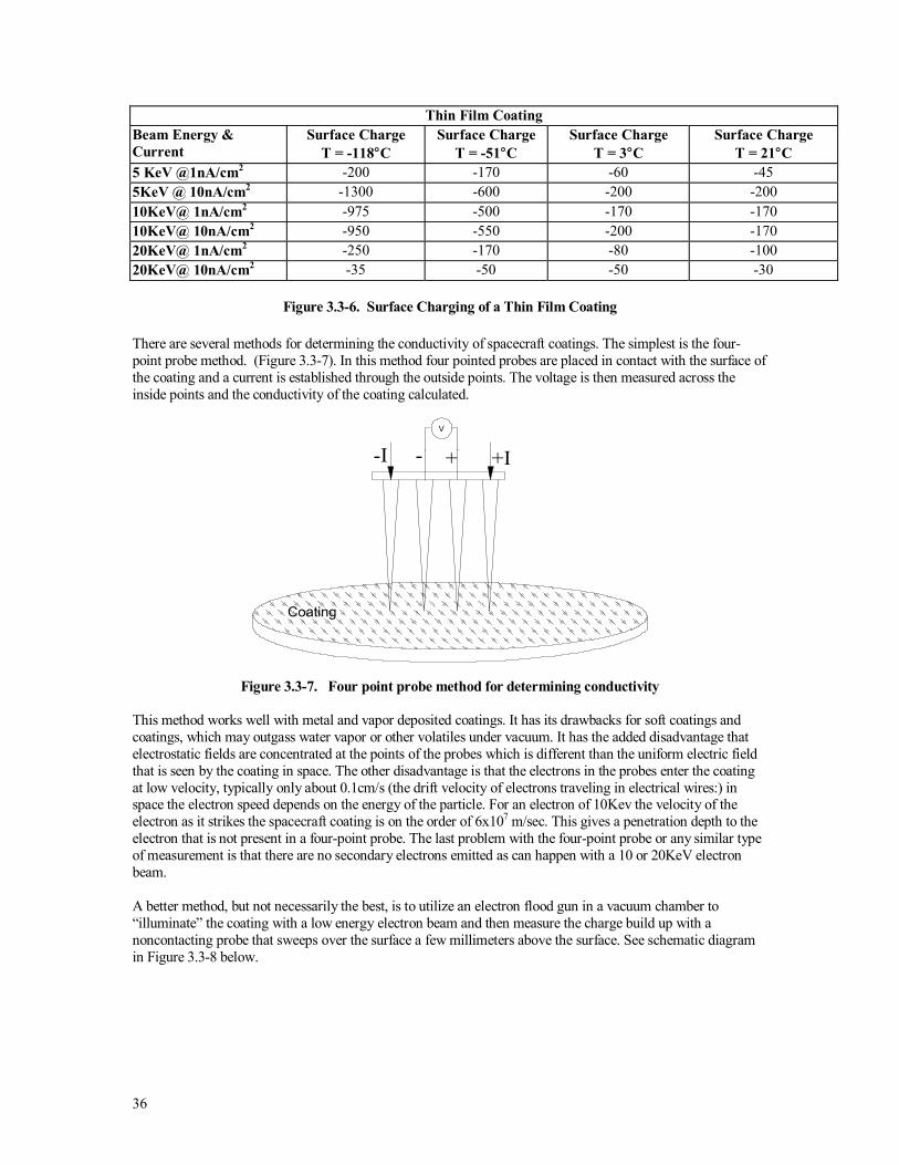
36
Thin Film Coating Beam Energy & Current
Surface Charge T = -118°C
Surface Charge T = -51°C
Surface Charge T = 3°C
Surface Charge T = 21°C
5 KeV @1nA/cm2 -200 -170 -60 -45 5KeV @ 10nA/cm2 -1300 -600 -200 -200 10KeV@ 1nA/cm2 -975 -500 -170 -170 10KeV@ 10nA/cm2 -950 -550 -200 -170 20KeV@ 1nA/cm2 -250 -170 -80 -100 20KeV@ 10nA/cm2 -35 -50 -50 -30
Figure 3.3-6. Surface Charging of a Thin Film Coating
There are several methods for determining the conductivity of spacecraft coatings. The simplest is the four-point probe method. (Figure 3.3-7). In this method four pointed probes are placed in contact with the surface of the coating and a current is established through the outside points. The voltage is then measured across the inside points and the conductivity of the coating calculated.
-I +IV
Coating
+-
Figure 3.3-7. Four point probe method for determining conductivity
This method works well with metal and vapor deposited coatings. It has its drawbacks for soft coatings and coatings, which may outgass water vapor or other volatiles under vacuum. It has the added disadvantage that electrostatic fields are concentrated at the points of the probes which is different than the uniform electric field that is seen by the coating in space. The other disadvantage is that the electrons in the probes enter the coating at low velocity, typically only about 0.1cm/s (the drift velocity of electrons traveling in electrical wires:) in space the electron speed depends on the energy of the particle. For an electron of 10Kev the velocity of the electron as it strikes the spacecraft coating is on the order of 6x10⁷ m/sec. This gives a penetration depth to the electron that is not present in a four-point probe. The last problem with the four-point probe or any similar type of measurement is that there are no secondary electrons emitted as can happen with a 10 or 20KeV electron beam. A better method, but not necessarily the best, is to utilize an electron flood gun in a vacuum chamber to illuminate the coating with a low energy electron beam and then measure the charge build up with a noncontacting probe that sweeps over the surface a few millimeters above the surface. See schematic diagram in Figure 3.3-8 below.
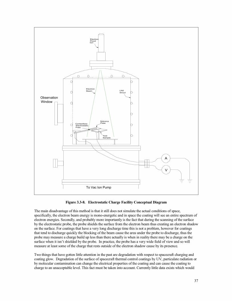
37
To Vac Ion Pump
LN2
ObservationWindow
A
V
Shroud
ElectronBeam
TestSample
ElectrostaticContactless
Probe
ReferencePlate
ElectronFloodGun
Figure 3.3-8. Electrostatic Charge Facility Conceptual Diagram
The main disadvantage of this method is that it still does not simulate the actual conditions of space, specifically, the electron beam energy is mono-energetic and in space the coating will see an entire spectrum of electron energies. Secondly, and probably more importantly is the fact that during the scanning of the surface by the electrostatic probe, the probe shields the surface from the electron beam thus creating an electron shadow on the surface. For coatings that have a very long discharge time this is not a problem, however for coatings that tend to discharge quickly the blocking of the beam cause the area under the probe to discharge, thus the probe may measure a charge build up less than there actually is when in reality there may be a charge on the surface when it isnt shielded by the probe. In practice, the probe has a very wide field of view and so will measure at least some of the charge that rests outside of the electron shadow cause by its presence. Two things that have gotten little attention in the past are degradation with respect to spacecraft charging and coating glow. Degradation of the surface of spacecraft thermal control coatings by UV, particulate radiation or by molecular contamination can change the electrical properties of the coating and can cause the coating to charge to an unacceptable level. This fact must be taken into account. Currently little data exists which would

38
give any indication how electrical conductivity changes with respect to various degradation environments. Coating glow can happen for certain coatings when incoming electrons of sufficient energy cause the surface to luminesce. This can be easily seen during an electron gun illumination. This glow can be quite bright at times and may need to be considered during future missions.
39
References
1. Siegel, Robert , Howell, John R., Thermal Radiation Heat Transfer volume 1, The
Blackbody, Electromagnetic and Material Properties, National Aeronautics and Space Administration, Washington DC, 1968
2. Jackson, J.D., Classical Electrodynamics, Second Edition, John Wiley Company, New York, 1975
3. Davis,Harry F., Snider, Arthur David, Introduction to Vector Analysis, forth edition, Allyn
and Bacon Inc. , Boston, 1979
4. Complex Variables and Applications third edition, Ruel V. Churchill, James W. Brown and Roger F. Verhey, McGraw-Hill, New York, 1976
5. Handbook of Heat Transfer Vol 1 & II, Max Jacob, John Wiley and Sons, New York, 1957
6. Edwards, D.K., J.T. Gier, K.E. Nelson, and R.D. Roddick, Integrating Sphere for Imperfectly
Diffuse Samples, Applied Optics, 51, November 1961
7. Henninger, John H., Solar Absorptance and Thermal Emittance of Some Common Spacecraft Thermal-Control Coatings, NASA Reference Publication 1121, National Aeronautics and Space Administration, Goddard Space Flight Center, Greenbelt Maryland, April 1984
8. 2000 ASTM Standard Extraterrestrial Spectrum Reference E-490-00
9. Characteristics and use of Infrared Detectors, Technical Information SD-12, Hamamatsu
10. Total Emittance Measurement Portable, Temp 200A, Operations Manual, AZ Technology,
Huntsville, Al, August 2002
11. Introduction to the Space Environment second edition, Thomas F. Tascione, Krieger Publishing Company, Makabar Florida, 1994
12. Introduction to Space Physics, edited by Margaret G. Kivelson and Christopher T. Russell,
Cambridge University Press, New York, 1995
13. Space and Planetary Environment Criteria. Guidelines for Use in Space Vehicle Development, R.E. Smith and G.S. West, 1982, NASA Technical Memorandum 82478.
14. Surface Charging / ESD Analysis, Preferred Reliability Practices, Practice No. PD-AP-1301,
NASA,
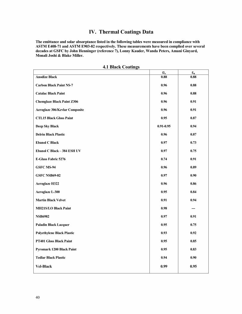
40
IV. Thermal Coatings Data The emittance and solar absorptance listed in the following tables were measured in compliance with ASTM E408-71 and ASTM E903-82 respectively. These measurements have been complied over several decades at GSFC by John Henninger (reference 7), Lonny Kauder, Wanda Peters, Amani Ginyard, Monali Joshi & Blake Miller.
4.1 Black Coatings
αs εn Anodize Black Carbon Black Paint NS-7 Catalac Black Paint Chemglaze Black Paint Z306 Aeroglaze 306/Kevlar Composite CTL15 Black Gloss Paint Deep Sky Black Delrin Black Plastic Ebanol C Black Ebanol C Black 384 ESH UV E-Glass Fabric 5276 GSFC MS-94 GSFC NSB69-82 Aeroglaze H322 Aeroglaze L-300 Martin Black Velvet MH21S/LO Black Paint NSB6982 Paladin Black Lacquer Polyethylene Black Plastic PT401 Gloss Black Paint Pyromark 1200 Black Paint Tedlar Black Plastic Vel-Black
0.88
0.96
0.96
0.96
0.96
0.95
0.91-0.95
0.96
0.97
0.97
0.74
0.96
0.97
0.96
0.95
0.91
0.98
0.97
0.95
0.93
0.95
0.95
0.94
0.99
0.88
0.88
0.88
0.91
0.91
0.87
0.94
0.87
0.73
0.75
0.91
0.89
0.90
0.86
0.84
0.94
---
0.91
0.75
0.92
0.85
0.83
0.90
0.95
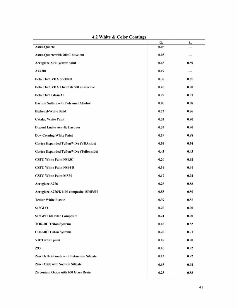
41
4.2 White & Color Coatings
αs εn Astro-Quartz Astro-Quartz with 900 C bake out Aeroglaze A971 yellow paint AZ4301 Beta Cloth/VDA Sheldahl Beta Cloth/VDA Chemfab 500 no silicone Beta Cloth Glass/Al Barium Sulfate with Polyvinyl Alcohol Biphenyl-White Solid Catalac White Paint Dupont Lucite Acrylic Lacquer Dow Corning White Paint Gortex Expanded Teflon/VDA (VDA side) Gortex Expanded Teflon/VDA (Teflon side) GSFC White Paint NS43C GSFC White Paint NS44-B GSFC White Paint MS74 Aeroglaze A276 Aeroglaze A276/K1100 composite 1500ESH Tedlar White Plastic S13GLO S13GPLO/Kevlar Composite TOR-RC Triton Systems COR-RC Triton Systems YB71 white paint Z93 Zinc Orthotitanate with Potassium Silicate Zinc Oxide with Sodium Silicate Zirconium Oxide with 650 Glass Resin
0.06
0.03
0.43
0.19
0.38
0.45
0.29
0.06
0.23
0.24
0.35
0.19
0.54
0.43
0.20
0.34
0.17
0.26
0.53
0.39
0.20
0.21
0.18
0.28
0.18
0.16
0.13
0.15
0.23
---
---
0.89
---
0.85
0.90
0.91
0.88
0.86
0.90
0.90
0.88
0.54
0.43
0.92
0.91
0.92
0.88
0.89
0.87
0.90
0.90
0.82
0.71
0.90
0.92
0.92
0.92
0.88
42
4.3 Conductive Paints αs εn Electrodag GSFC NS43G NS43G/Hincom GSFC Green NS53-B GSFC Green NS43-E GSFC White NS43C GSFC Green NS55-F GSFC Green NS-79 Z93SC55
0.90
0.26
0.18
0.52
0.57
0.20
0.57
0.57
0.14
0.68
0.90
0.92
0.87
0.89
0.92
0.91
0.91
0.94
43
4.4 Anodized Aluminum Coatings αs εn Black Black Black AnoBlack Black 0.0001mils 0.0005mils 0.001mils Black Anodize with sealer 0.001mils 0.002mils 1.5 mils Blue Blue Brown Chromic Clear Clear Clear/ 7075 Aluminum Clear 0.0001mils 0.0005mils 0.001mils Clear Type 2 Class 1 Clear with sealer 0.001mils 0.002mils 1.5mils Green Gold Gold 0.0001mils 0.0005mils 0.001mils Hard Anodize Aluminum 7075-T6 Aluminum 6061-T6 Aluminum 2024-T6 Plain Red Sulphuric Yellow Blue Anodized Titanium Foil
0.65 0.86 0.94
0.51 0.60 0.67
0.71 0.70 0.73 0.67 0.53 0.73 0.44 0.27 0.35 0.68
0.32 0.37 0.44 0.43
0.50 0.70 0.59 0.66 0.48
0.40 0.46 0.52
0.83 0.90 0.76 0.26 0.57 0.42 0.47 0.70
0.82 0.86 0.89
0.75 0.82 0.84
0.84 0.86 0.86 0.87 0.82 0.86 0.56 0.76 0.84 0.82
0.75 0.81 0.85 0.67
0.84 0.86 0.87 0.88 0.82
0.74 0.81 0.82
0.87 0.86 0.90 0.04 0.88 0.87 0.87 0.13
44
4.5 Metals and Conversion Coatings αs εn Alodyne Aluminum 2024 Alodyne Aluminum 6061-T2 Aluminum Polished Alzac A-2 Alzac A-5 Alodine Beryllium Beryllium Copper Oxidized Beryllium Lathe finish Lap finish Wire finish Milled finish Black Chrome Black Copper Black Irridite Black Nickel Black Nickel/ZK60Mg Black Nickel/Magnesium Black Nickel/Titanium Buffed Aluminum Buffed Copper Constantan- Metal Strip Copper Foil Tape Plain Sanded Tarnished Dow 7 on Polished Magnesium Dow 7 on Sanded Magnesium Dow 9 on Magnesium Dow 23 on Magnesium Ebanol C Black Electroplated Gold Electrolytic Gold Electroless Nickel Gold Plated Beryllium Mirror Irridite Aluminum Irridite Aluminum Inconel X Foil Kannigen-Nickel Alloy Mu metal Plain Beryllium Copper Platinum Foil Stainless Steel Polished Machined Sandblasted Machine Rolled Boom-Polished 1-mil 304 Foil Tantalum Foil TiN/Titanium Titanium Anodized Tiodize Titanium TinFin400 Tiodize Titanium TinFin200 Tungsten Polished
0.42 0.44 0.14 0.88 0.18
0.68 - 0.76 0.83 - 0.87
0.51 0.71 0.77 0.52 0.96 0.98 0.62 0.91
0.78 0.80 0.92 0.91 0.16 0.30 0.37
0.32 0.26 0.55 --- --- ---
0.62 0.97 0.23 0.20 0.39 0.21 ---
0.24 0.52 0.45 ---
0.31 0.33
0.42 0.47 0.58 0.39 0.44 0.40 0.40 0.52
0.84 0.86 0.74 0.74 0.44
0.10 0.14 0.03 0.88 ---
0.06 - 0.15 0.09
0.05 0.12 0.28 0.07 0.62 0.63 0.17 0.66
0.56 0.61 0.74 0.77 0.03 0.03 0.09
0.02 0.04 0.04 0.49 0.65 0.87 0.67 0.77 0.03 0.02 0.07 0.03 0.11 0.04 0.10 0.08 0.09 0.03 0.04
0.11 0.14 0.38 0.11 0.10 0.05 0.05 0.11
0.44 0.48 0.73 0.23 0.03
45
4.6 Vapor Deposited Coatings * αs εn Aluminum Aluminum on Black Kapton Aluminum on Fiberglass Aluminum on Stainless Steel Aluminum on Lacquer Aluminum on abraded Lacquer Chromium Chromium on 5-mil Kapton Germanium Gold Iron Oxide Molybdenum Nickel Rhodium Silver Titanium Tungsten
0.08
0.12
0.15
0.08
0.08
0.33
0.56
0.57
0.52
0.19
0.85
0.56
0.38
0.18
0.04
0.52
0.60
0.02
0.03
0.07
0.02
0.02
0.07
0.17
0.24
0.09
0.02
0.56
0.21
0.04
0.03
0.02
0.12
0.27
* on glass substrates except where noted
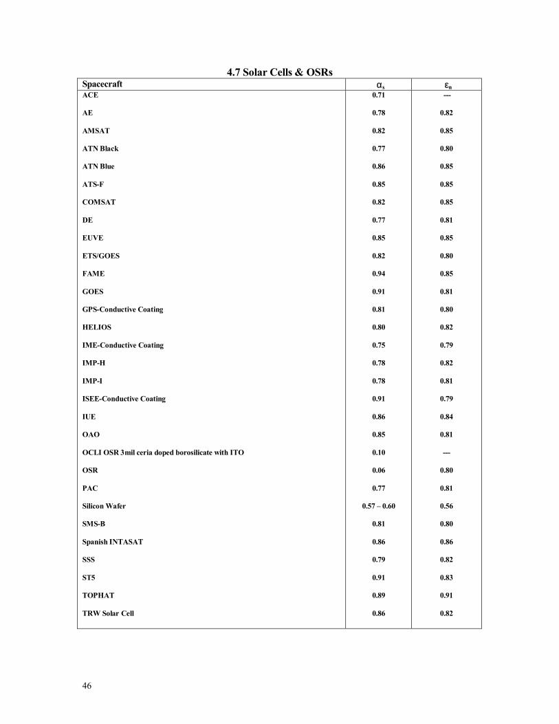
46
4.7 Solar Cells & OSRs Spacecraft αs εn ACE AE AMSAT ATN Black ATN Blue ATS-F COMSAT DE EUVE ETS/GOES FAME GOES GPS-Conductive Coating HELIOS IME-Conductive Coating IMP-H IMP-I ISEE-Conductive Coating IUE OAO OCLI OSR 3mil ceria doped borosilicate with ITO OSR PAC Silicon Wafer SMS-B Spanish INTASAT SSS ST5 TOPHAT TRW Solar Cell
0.71
0.78
0.82
0.77
0.86
0.85
0.82
0.77
0.85
0.82
0.94
0.91
0.81
0.80
0.75
0.78
0.78
0.91
0.86
0.85
0.10
0.06
0.77
0.57 0.60
0.81
0.86
0.79
0.91
0.89
0.86
---
0.82
0.85
0.80
0.85
0.85
0.85
0.81
0.85
0.80
0.85
0.81
0.80
0.82
0.79
0.82
0.81
0.79
0.84
0.81
---
0.80
0.81
0.56
0.80
0.86
0.82
0.83
0.91
0.82
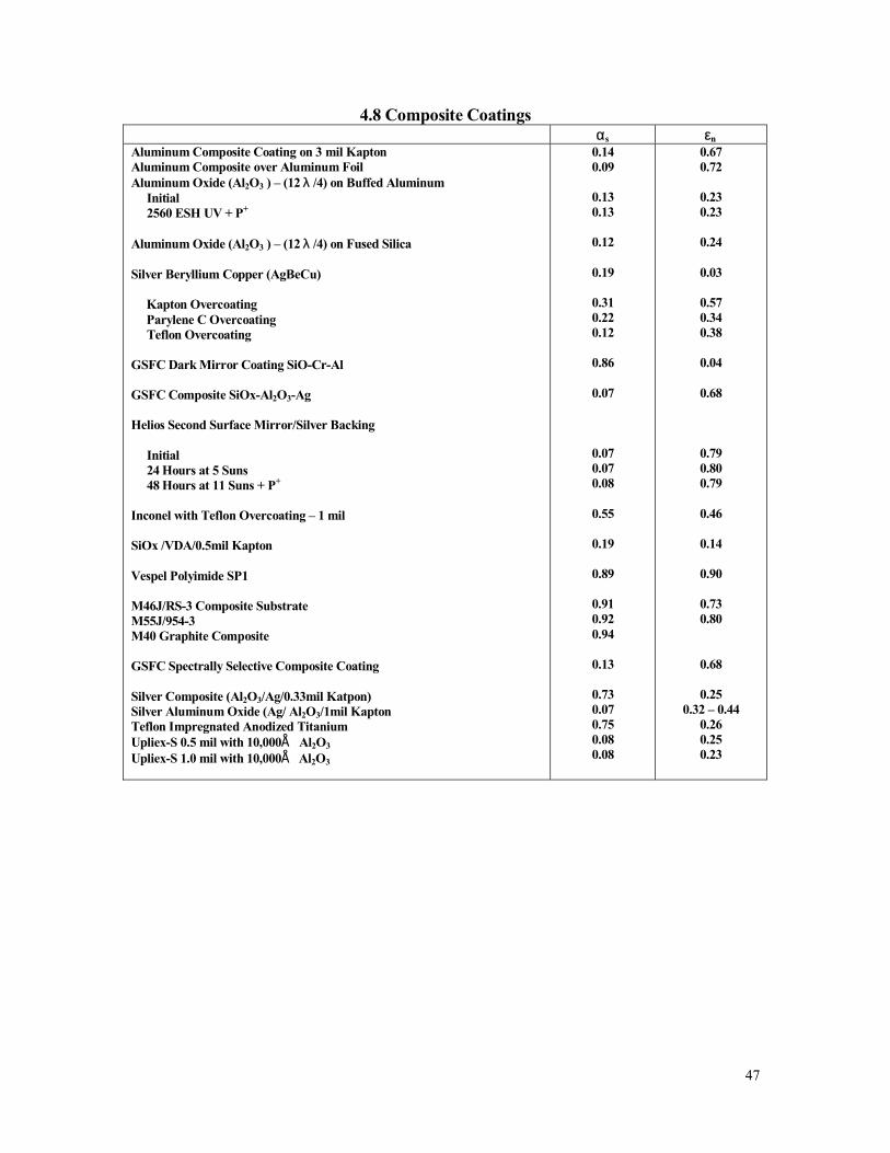
47
4.8 Composite Coatings αs εn Aluminum Composite Coating on 3 mil Kapton Aluminum Composite over Aluminum Foil Aluminum Oxide (Al2O3 ) (12 λ /4) on Buffed Aluminum Initial 2560 ESH UV + P+ Aluminum Oxide (Al2O3 ) (12 λ /4) on Fused Silica Silver Beryllium Copper (AgBeCu) Kapton Overcoating Parylene C Overcoating Teflon Overcoating GSFC Dark Mirror Coating SiO-Cr-Al GSFC Composite SiOx-Al2O3-Ag Helios Second Surface Mirror/Silver Backing Initial 24 Hours at 5 Suns 48 Hours at 11 Suns + P+ Inconel with Teflon Overcoating 1 mil SiOx /VDA/0.5mil Kapton Vespel Polyimide SP1 M46J/RS-3 Composite Substrate M55J/954-3 M40 Graphite Composite GSFC Spectrally Selective Composite Coating Silver Composite (Al2O3/Ag/0.33mil Katpon) Silver Aluminum Oxide (Ag/ Al2O3/1mil Kapton Teflon Impregnated Anodized Titanium Upliex-S 0.5 mil with 10,000Å Al2O3 Upliex-S 1.0 mil with 10,000Å Al2O3
0.14 0.09
0.13 0.13
0.12
0.19
0.31 0.22 0.12
0.86
0.07
0.07 0.07 0.08
0.55
0.19
0.89
0.91 0.92 0.94
0.13
0.73 0.07 0.75 0.08 0.08
0.67 0.72
0.23 0.23
0.24
0.03
0.57 0.34 0.38
0.04
0.68
0.79 0.80 0.79
0.46
0.14
0.90
0.73 0.80
0.68
0.25 0.32 0.44
0.26 0.25 0.23
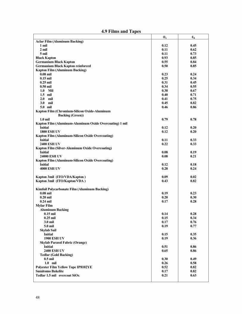
48
4.9 Films and Tapes αs εn Aclar Film (Aluminum Backing) 1 mil 2 mil 5 mil Black Kapton Germanium Black Kapton Germanium Black Kapton reinforced Kapton Film (Aluminum Backing) 0.08 mil 0.15 mil 0.25 mil 0.50 mil
1.0 Mil 1.5 mil 2.0 mil 3.0 mil 5.0 mil
Kapton Film (Chromium-Silicon Oxide-Aluminum Backing (Green)) 1.0 mil Kapton Film (Aluminum-Aluminum Oxide Overcoating) 1 mil Initial 1800 ESH UV Kapton Film (Aluminum-Silicon Oxide Overcoating) Initial 2400 ESH UV Kapton Film (Silver-Aluminum Oxide Overcoating) Initial 24000 ESH UV Kapton Film (Aluminum-Silicon Oxide Overcoating) Initial 4000 ESH UV Kapton 3mil (ITO/VDA/Kapton ) Kapton 3mil (ITO/Kapton/VDA ) Kimfoil Polycarbonate Film (Aluminum Backing) 0.08 mil 0.20 mil 0.24 mil Mylar Film Aluminum Backing 0.15 mil 0.25 mil 3.0 mil 5.0 mil Skylab Sail Initial 1900 ESH UV Skylab Parasol Fabric (Orange) Initial 2400 ESH UV Tedlar (Gold Backing) 0.5 mil
1.0 mil Polyester Film Yellow Tape IP8102YE Sumitomo Bakelite Tedlar 1.5 mil overcoat SiOx
0.12 0.11 0.11 0.93 0.55 0.50
0.23 0.25 0.31 0.34 0.38 0.40 0.41 0.45 0.46
0.79
0.12 0.12
0.11 0.22
0.08 0.08
0.12 0.28
0.09 0.43
0.19 0.20 0.17
0.14 0.15 0.17 0.19
0.15 0.19
0.51 0.65
0.30 0.26 0.52 0.17 0.21
0.45 0.62 0.73 0.85 0.84 0.85
0.24 0.34 0.45 0.55 0.67 0.71 0.75 0.82 0.86
0.78
0.20 0.20
0.33 0.33
0.19 0.21
0.18 0.24
0.02 0.82
0.23 0.30 0.28
0.28 0.34 0.76 0.77
0.35 0.36
0.86 0.86
0.49 0.58 0.82 0.82 0.63
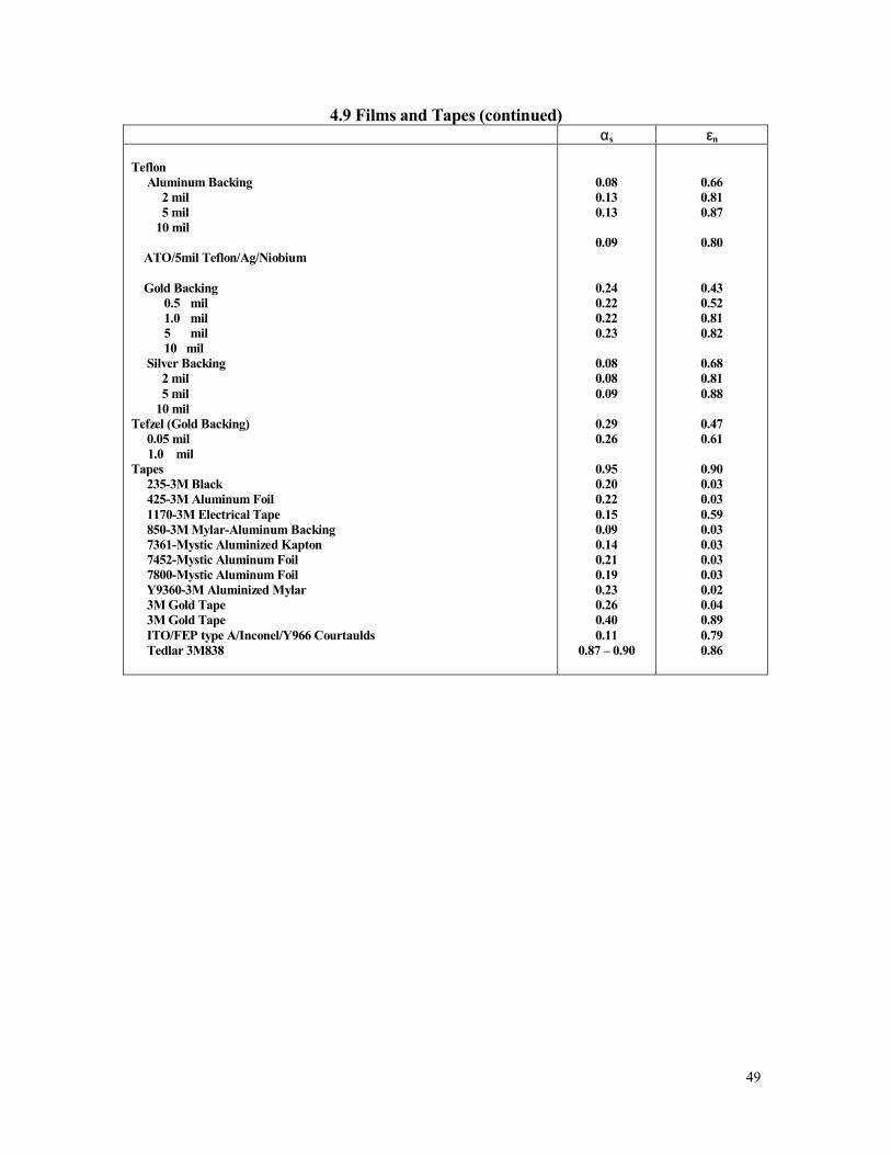
49
4.9 Films and Tapes (continued) αs εn Teflon Aluminum Backing 2 mil 5 mil 10 mil ATO/5mil Teflon/Ag/Niobium Gold Backing
0.5 mil 1.0 mil 5 mil 10 mil
Silver Backing 2 mil 5 mil 10 mil Tefzel (Gold Backing) 0.05 mil
1.0 mil Tapes 235-3M Black 425-3M Aluminum Foil 1170-3M Electrical Tape 850-3M Mylar-Aluminum Backing 7361-Mystic Aluminized Kapton 7452-Mystic Aluminum Foil 7800-Mystic Aluminum Foil Y9360-3M Aluminized Mylar 3M Gold Tape 3M Gold Tape ITO/FEP type A/Inconel/Y966 Courtaulds Tedlar 3M838
0.08 0.13 0.13
0.09
0.24 0.22 0.22 0.23
0.08 0.08 0.09
0.29 0.26
0.95 0.20 0.22 0.15 0.09 0.14 0.21 0.19 0.23 0.26 0.40 0.11
0.87 0.90
0.66 0.81 0.87
0.80
0.43 0.52 0.81 0.82
0.68 0.81 0.88
0.47 0.61
0.90 0.03 0.03 0.59 0.03 0.03 0.03 0.03 0.02 0.04 0.89 0.79 0.86

50
V. Total Hemispherical Reflectance Curves for Selected Thermal Control Coatings
The reflectance measurements contained in the following pages represents a compilation of reflectance measurements of commonly used thermal control coatings compiled at GSFC over a period of 20 years. The data was compiled using a variety of instruments, including a Beckman DK2, Perkin-Elmer Lamda-9, AZ-Tek LPSR 200 & 300 and was collected by John Henninger, Lonny Kauder, Wanda Peters, Amani Ginyard, Monali Joshi, & Blake Miller . The accuracy of the reflectance measurements is generally ±0.02.
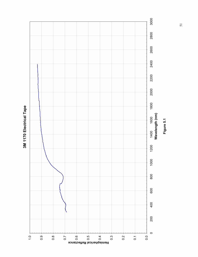
51
3M 1
170
Elec
tric
al T
ape
0.0
0.1
0.2
0.3
0.4
0.5
0.6
0.7
0.8
0.9
1.0
020
040
060
080
010
0012
0014
0016
0018
0020
0022
0024
0026
0028
0030
00W
avel
engt
h (n
m)
Figu
re 5
.1
Hemispherical Reflectance
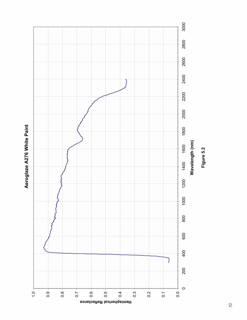
52
Aer
ogla
ze A
276
Whi
te P
aint
0.0
0.1
0.2
0.3
0.4
0.5
0.6
0.7
0.8
0.9
1.0
020
040
060
080
010
0012
0014
0016
0018
0020
0022
0024
0026
0028
0030
00
Wav
elen
gth
(nm
)
Figu
re 5
.2
Hemispherical Reflectance
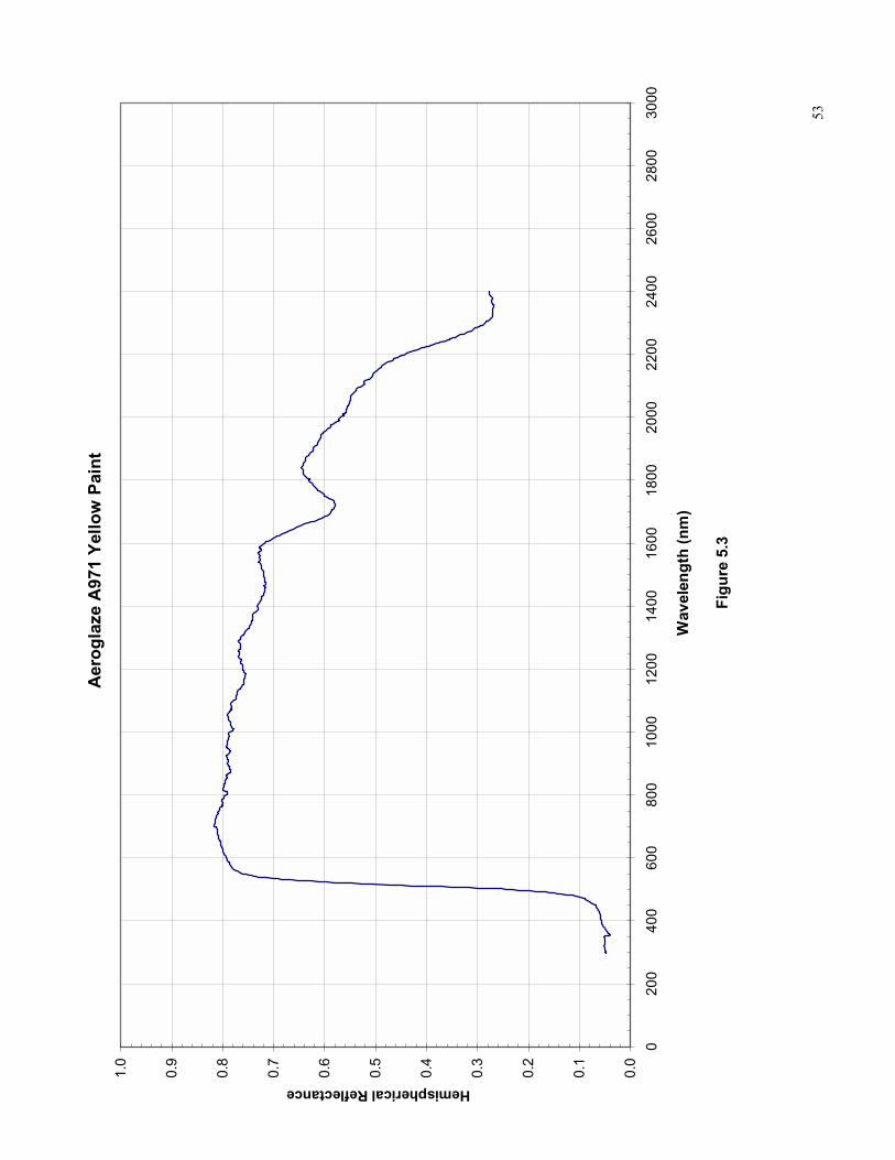
53
Aer
ogla
ze A
971
Yello
w P
aint
0.0
0.1
0.2
0.3
0.4
0.5
0.6
0.7
0.8
0.9
1.0
020
040
060
080
010
0012
0014
0016
0018
0020
0022
0024
0026
0028
0030
00
Wav
elen
gth
(nm
)
Figu
re 5
.3
Hemispherical Reflectance
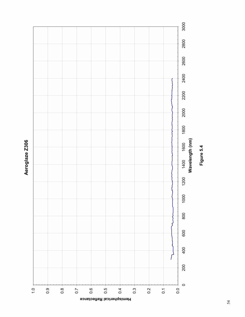
54
Aer
ogla
ze Z
306
0.0
0.1
0.2
0.3
0.4
0.5
0.6
0.7
0.8
0.9
1.0
020
040
060
080
010
0012
0014
0016
0018
0020
0022
0024
0026
0028
0030
00W
avel
engt
h (n
m)
Figu
re 5
.4
Hemispherical Reflectance
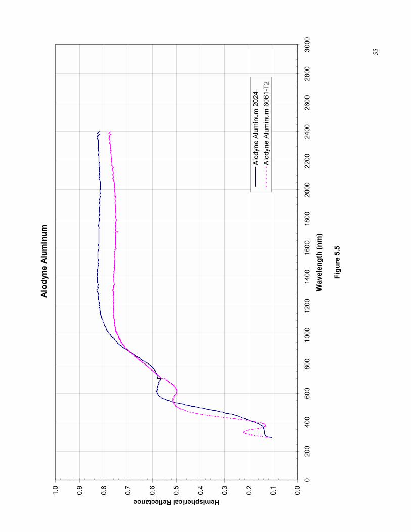
55
Alo
dyne
Alu
min
um
0.0
0.1
0.2
0.3
0.4
0.5
0.6
0.7
0.8
0.9
1.0
020
040
060
080
010
0012
0014
0016
0018
0020
0022
0024
0026
0028
0030
00
Wav
elen
gth
(nm
)
Figu
re 5
.5
Hemispherical Reflectance
Alo
dyne
Alu
min
um 2
024
Alo
dyne
Alu
min
um 6
061-
T2
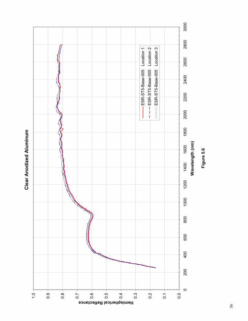
56
Cle
ar A
nodi
zed
Alu
min
um
0.0
0.1
0.2
0.3
0.4
0.5
0.6
0.7
0.8
0.9
1.0
020
040
060
080
010
0012
0014
0016
0018
0020
0022
0024
0026
0028
0030
00
Wav
elen
gth
(nm
)
Figu
re 5
.6
Hemispherical Reflectance
ES
R-S
T5-B
ase-
005
Loc
atio
n 1
ES
R-S
T5-B
ase-
005
Loc
atio
n 2
ES
R-S
T5-B
ase-
005
Loc
atio
n 3
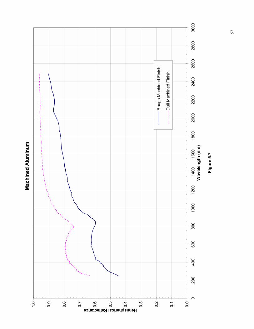
57
Mac
hine
d A
lum
inum
0.0
0.1
0.2
0.3
0.4
0.5
0.6
0.7
0.8
0.9
1.0
020
040
060
080
010
0012
0014
0016
0018
0020
0022
0024
0026
0028
0030
00W
avel
engt
h (n
m)
Figu
re 5
.7
Hemispherical Reflectance
Rou
gh M
achi
ned
Fini
sh
Dul
l Mac
hine
d Fi
nish
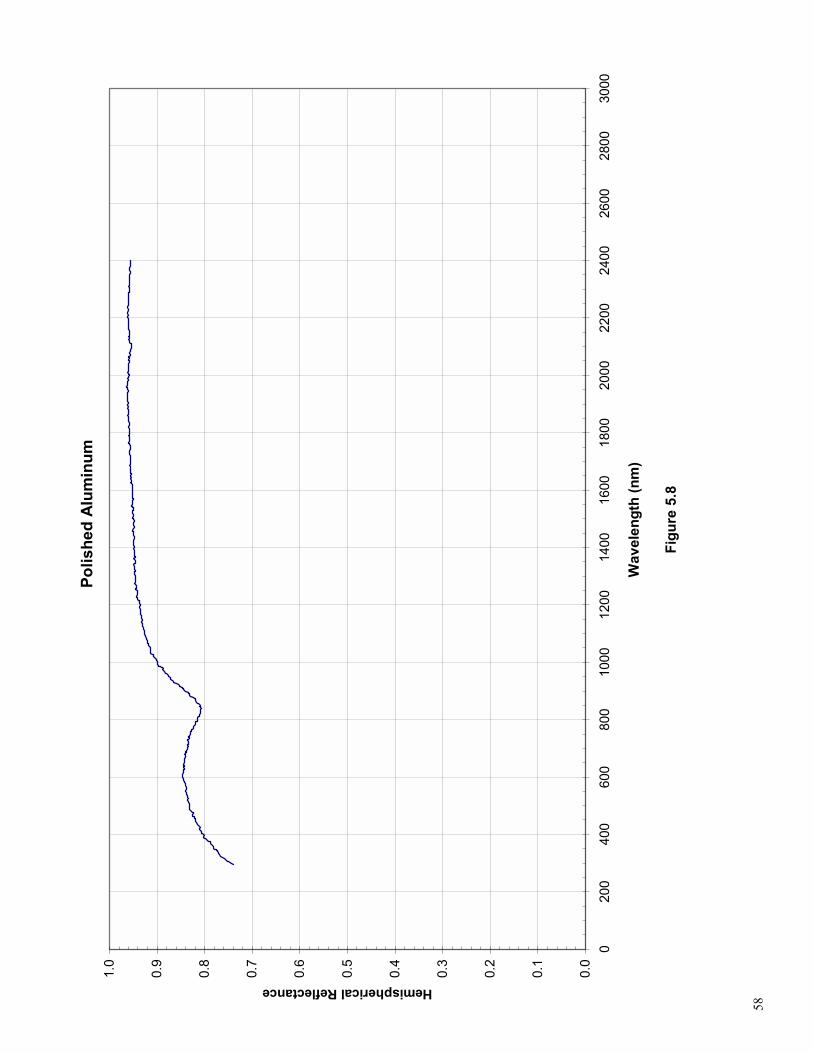
58
Polis
hed
Alu
min
um
0.0
0.1
0.2
0.3
0.4
0.5
0.6
0.7
0.8
0.9
1.0
020
040
060
080
010
0012
0014
0016
0018
0020
0022
0024
0026
0028
0030
00
Wav
elen
gth
(nm
)
Figu
re 5
.8
Hemispherical Reflectance
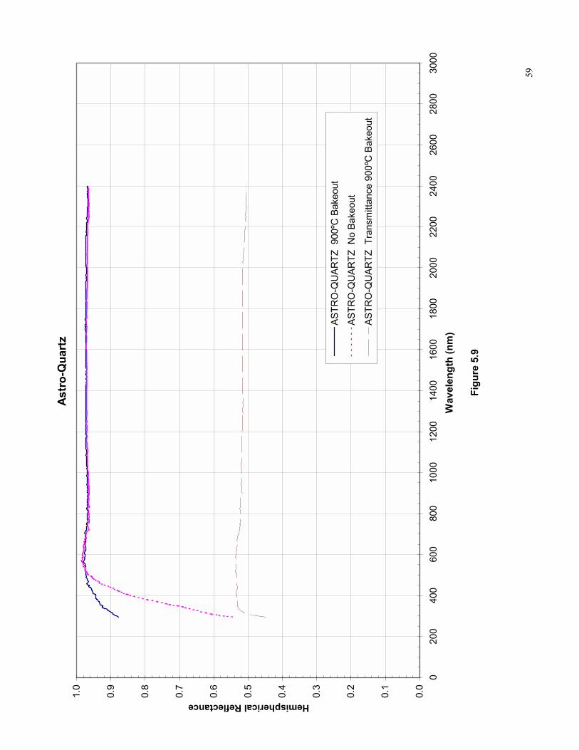
59
Ast
ro-Q
uart
z
0.0
0.1
0.2
0.3
0.4
0.5
0.6
0.7
0.8
0.9
1.0
020
040
060
080
010
0012
0014
0016
0018
0020
0022
0024
0026
0028
0030
00
Wav
elen
gth
(nm
)
Figu
re 5
.9
Hemispherical Reflectance
AS
TRO
-QU
AR
TZ 9
00ºC
Bak
eout
AS
TRO
-QU
AR
TZ N
o B
akeo
ut
AS
TRO
-QU
AR
TZ T
rans
mitt
ance
900
ºC B
akeo
ut
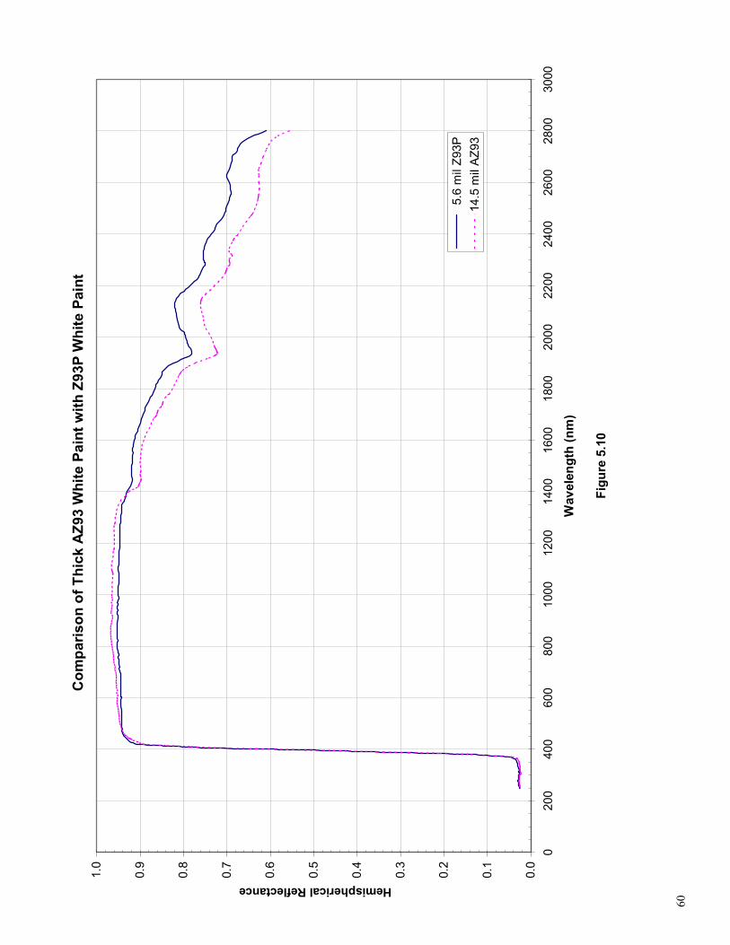
60
Com
paris
on o
f Thi
ck A
Z93
Whi
te P
aint
with
Z93
P W
hite
Pai
nt
0.0
0.1
0.2
0.3
0.4
0.5
0.6
0.7
0.8
0.9
1.0
020
040
060
080
010
0012
0014
0016
0018
0020
0022
0024
0026
0028
0030
00
Wav
elen
gth
(nm
)
Figu
re 5
.10
Hemispherical Reflectance
5.6
mil
Z93P
14.5
mil
AZ9
3
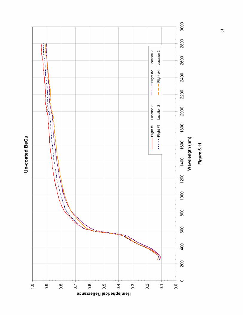
61
Un-
coat
ed B
eCu
0.0
0.1
0.2
0.3
0.4
0.5
0.6
0.7
0.8
0.9
1.0
020
040
060
080
010
0012
0014
0016
0018
0020
0022
0024
0026
0028
0030
00
Wav
elen
gth
(nm
)
Figu
re 5
.11
Hemispherical Reflectance
Flig
ht #
1
Loc
atio
n 2
Flig
ht #
2
Loc
atio
n 2
Flig
ht #
3
Loc
atio
n 2
Flig
ht #
4
Loc
atio
n 2
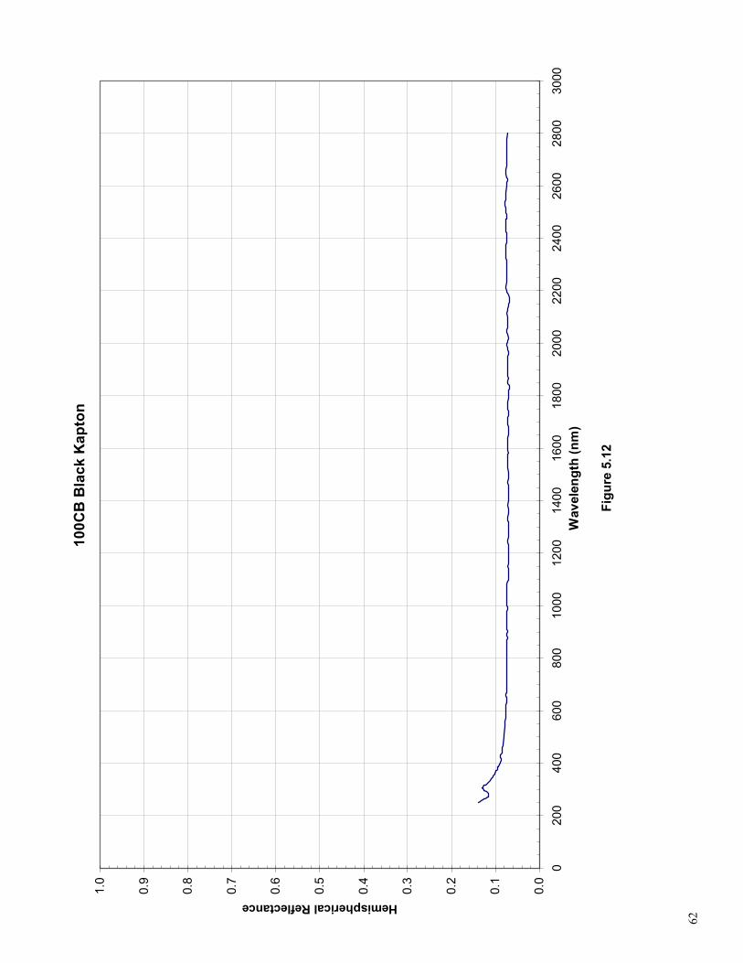
62
100
CB
Bla
ck K
apto
n
0.0
0.1
0.2
0.3
0.4
0.5
0.6
0.7
0.8
0.9
1.0
020
040
060
080
010
0012
0014
0016
0018
0020
0022
0024
0026
0028
0030
00W
avel
engt
h (n
m)
Figu
re 5
.12
Hemispherical Reflectance
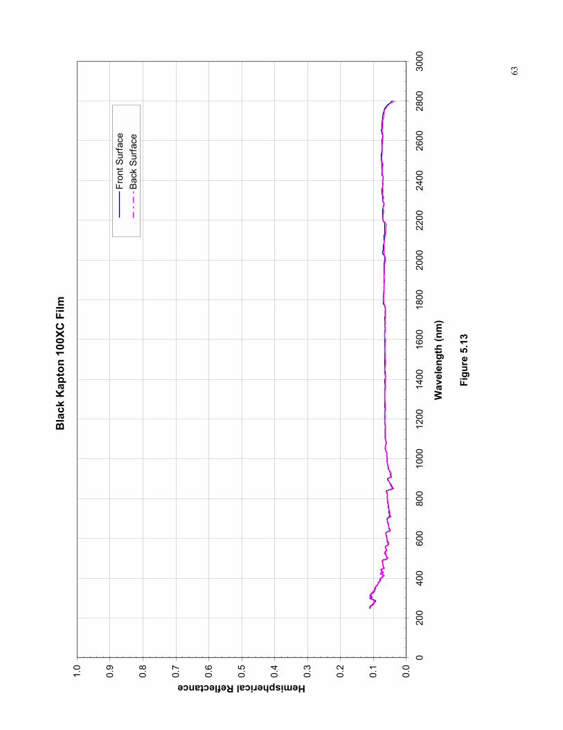
63
Bla
ck K
apto
n 10
0XC
Film
0.0
0.1
0.2
0.3
0.4
0.5
0.6
0.7
0.8
0.9
1.0
020
040
060
080
010
0012
0014
0016
0018
0020
0022
0024
0026
0028
0030
00
Wav
elen
gth
(nm
)
Figu
re 5
.13
Hemispherical Reflectance
Fron
t Sur
face
B
ack
Sur
face
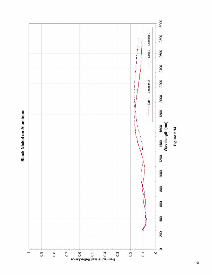
64
Bla
ck N
icke
l on
Alu
min
um
0
0.1
0.2
0.3
0.4
0.5
0.6
0.7
0.8
0.91
020
040
060
080
010
0012
0014
0016
0018
0020
0022
0024
0026
0028
0030
00W
avel
engt
h (n
m)
Figu
re 5
.14
Hemispherical Reflectance
Side
1
Loc
atio
n 2
Side
2
Loc
atio
n 2
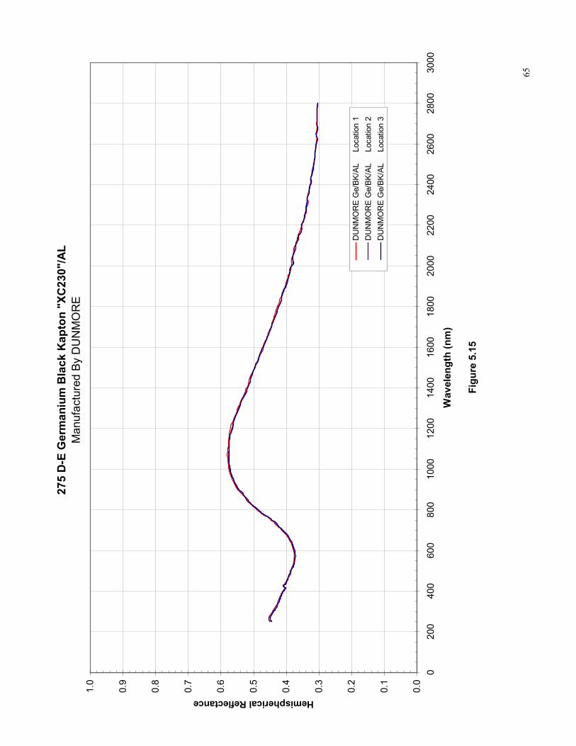
65
275
D-E
Ger
man
ium
Bla
ck K
apto
n "X
C23
0"/A
LM
anuf
actu
red
By D
UN
MO
RE
0.0
0.1
0.2
0.3
0.4
0.5
0.6
0.7
0.8
0.9
1.0
020
040
060
080
010
0012
0014
0016
0018
0020
0022
0024
0026
0028
0030
00
Wav
elen
gth
(nm
)
Figu
re 5
.15
Hemispherical Reflectance
DU
NM
OR
E G
e/BK
/AL
L
ocat
ion
1D
UN
MO
RE
Ge/
BK/A
L
Loc
atio
n 2
DU
NM
OR
E G
e/BK
/AL
L
ocat
ion
3
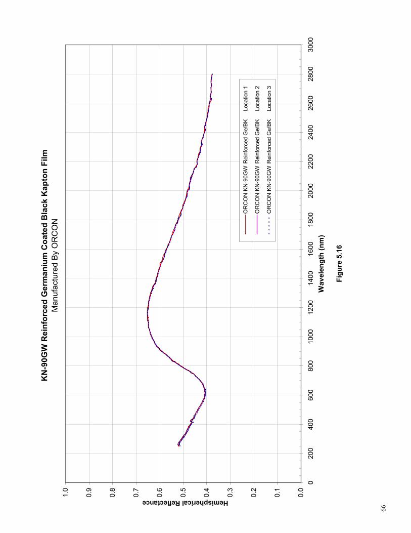
66
KN
-90G
W R
einf
orce
d G
erm
aniu
m C
oate
d B
lack
Kap
ton
Film
Man
ufac
ture
d By
OR
CO
N
0.0
0.1
0.2
0.3
0.4
0.5
0.6
0.7
0.8
0.9
1.0
020
040
060
080
010
0012
0014
0016
0018
0020
0022
0024
0026
0028
0030
00W
avel
engt
h (n
m)
Figu
re 5
.16
Hemispherical Reflectance
OR
CO
N K
N-9
0GW
Rei
nfor
ced
Ge/
BK
Loc
atio
n 1
OR
CO
N K
N-9
0GW
Rei
nfor
ced
Ge/
BK
Loc
atio
n 2
OR
CO
N K
N-9
0GW
Rei
nfor
ced
Ge/
BK
Loc
atio
n 3
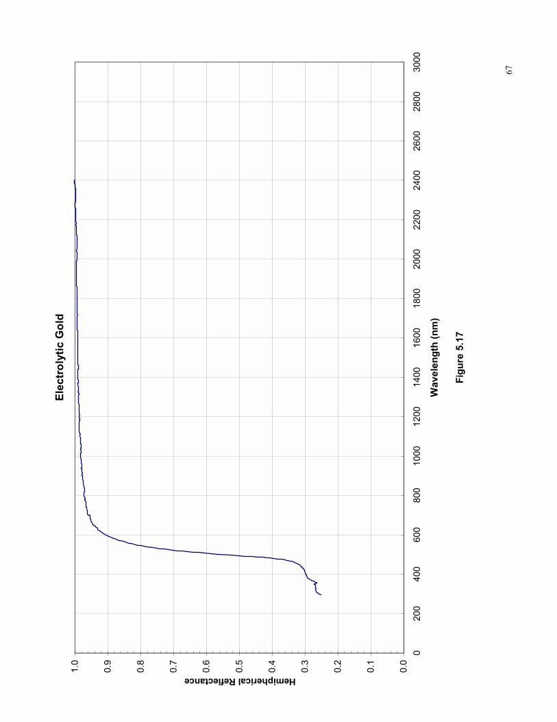
67
Elec
trol
ytic
Gol
d
0.0
0.1
0.2
0.3
0.4
0.5
0.6
0.7
0.8
0.9
1.0
020
040
060
080
010
0012
0014
0016
0018
0020
0022
0024
0026
0028
0030
00
Wav
elen
gth
(nm
)
Figu
re 5
.17
Hemipherical Reflectance
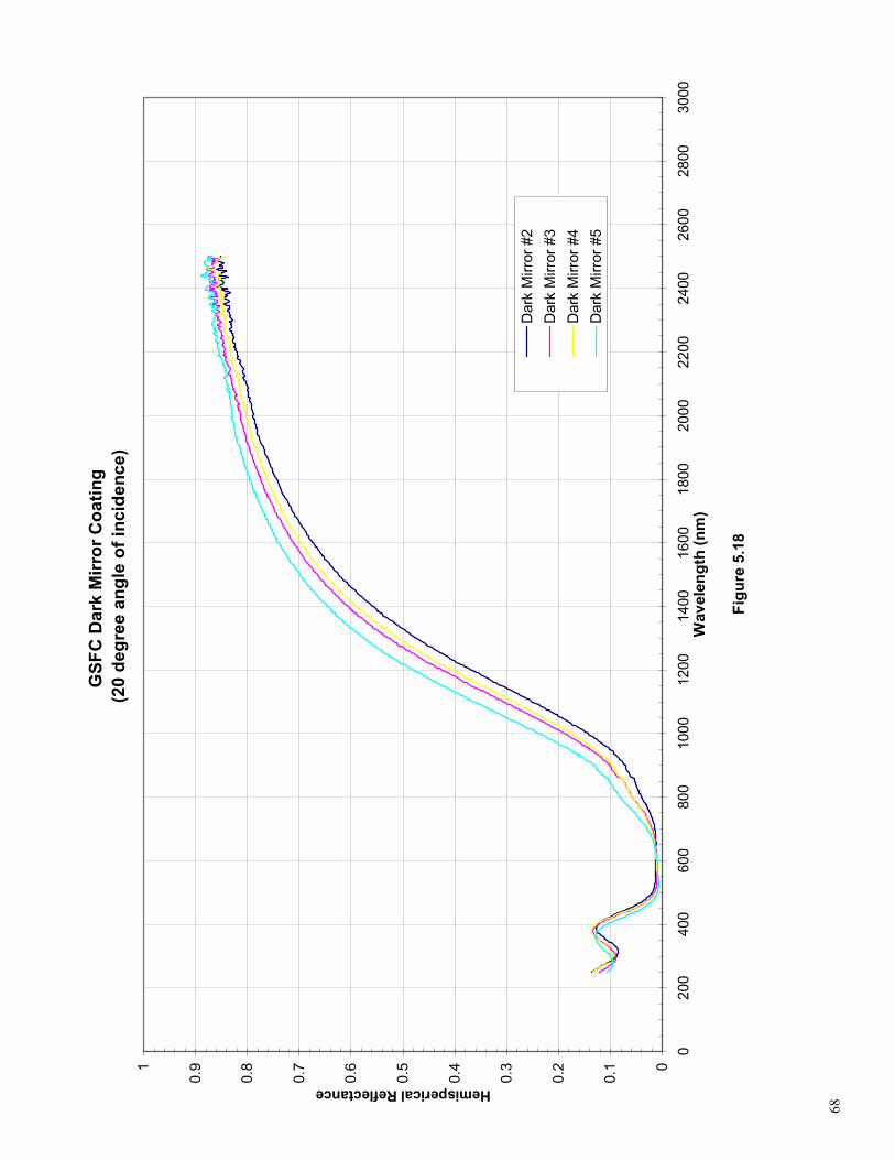
68
GSF
C D
ark
Mirr
or C
oatin
g (2
0 de
gree
ang
le o
f inc
iden
ce)
0
0.1
0.2
0.3
0.4
0.5
0.6
0.7
0.8
0.91
020
040
060
080
010
0012
0014
0016
0018
0020
0022
0024
0026
0028
0030
00W
avel
engt
h (n
m)
Figu
re 5
.18
Hemisperical Reflectance
Dar
k M
irror
#2
Dar
k M
irror
#3
Dar
k M
irror
#4
Dar
k M
irror
#5
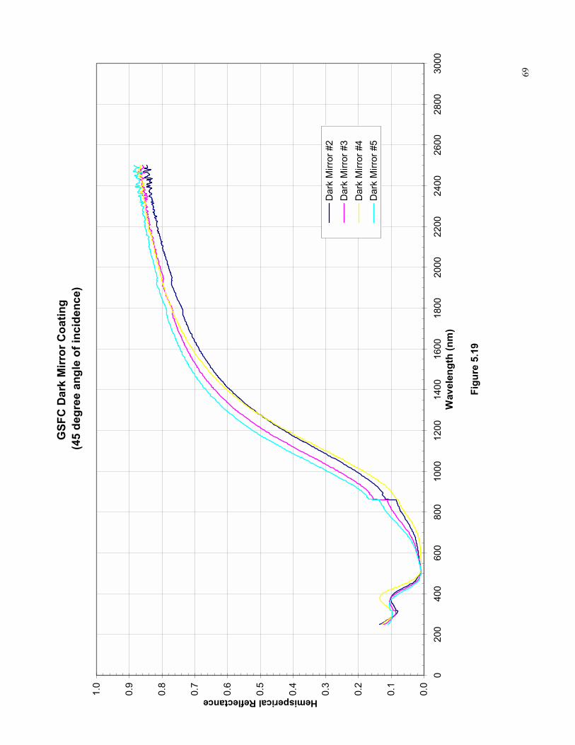
69
GSF
C D
ark
Mirr
or C
oatin
g (4
5 de
gree
ang
le o
f inc
iden
ce)
0.0
0.1
0.2
0.3
0.4
0.5
0.6
0.7
0.8
0.9
1.0
020
040
060
080
010
0012
0014
0016
0018
0020
0022
0024
0026
0028
0030
00W
avel
engt
h (n
m)
Figu
re 5
.19
Hemisperical Reflectance
Dar
k M
irror
#2
Dar
k M
irror
#3
Dar
k M
irror
#4
Dar
k M
irror
#5
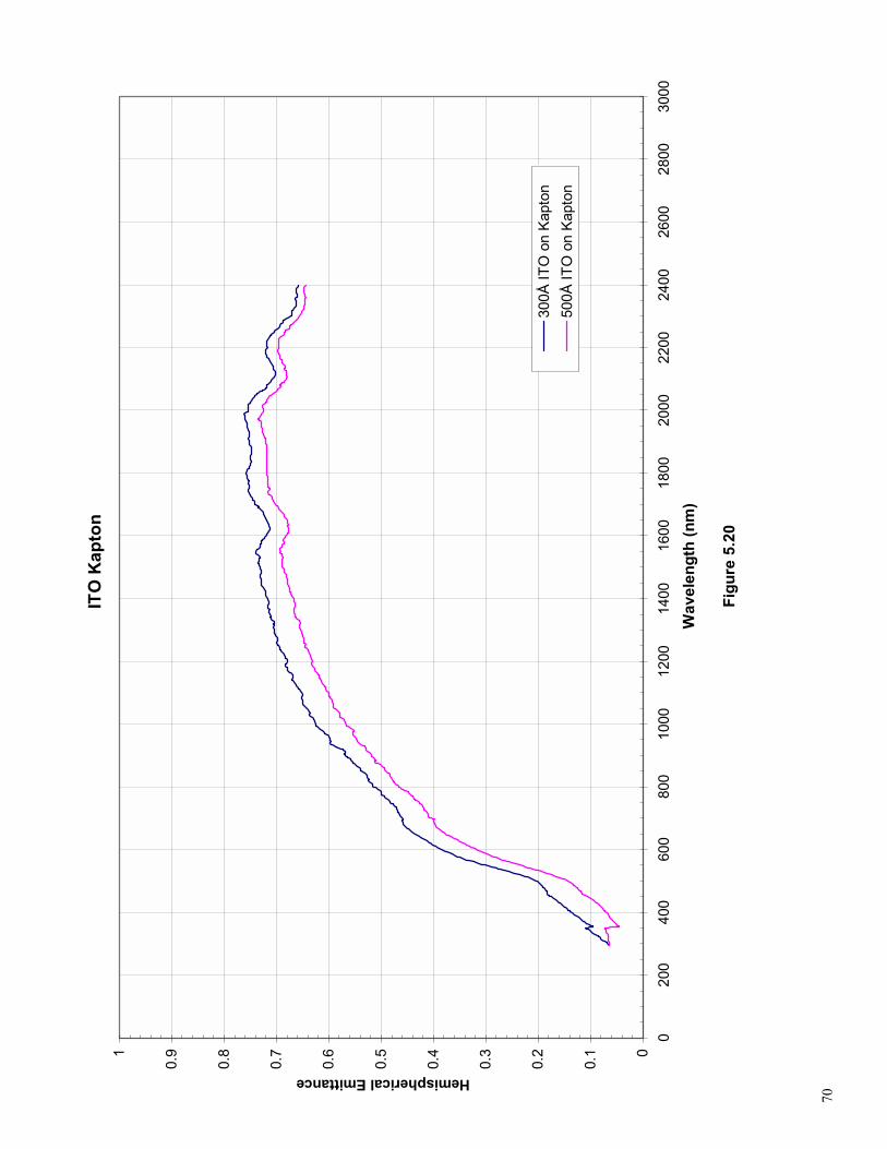
70
ITO
Kap
ton
0
0.1
0.2
0.3
0.4
0.5
0.6
0.7
0.8
0.91
020
040
060
080
010
0012
0014
0016
0018
0020
0022
0024
0026
0028
0030
00
Wav
elen
gth
(nm
)
Figu
re 5
.20
Hemispherical Emittance
300Å
ITO
on
Kap
ton
500Å
ITO
on
Kap
ton
71
SiO
x/K
apto
n
0.0
0.1
0.2
0.3
0.4
0.5
0.6
0.7
0.8
0.9
1.0
020
040
060
080
010
0012
0014
0016
0018
0020
0022
0024
0026
0028
0030
00
Wav
elen
gth
(nm
)
Figu
re 5
.21
Hermispherical Reflectance
750Å
SiO
x/K
apto
n15
00Å
SiO
x/K
apto
n22
50Å
SiO
x/K
apto
n
72
1500
Å S
iOx/
Kap
ton/
VDA
0.0
0.1
0.2
0.3
0.4
0.5
0.6
0.7
0.8
0.9
1.0
020
040
060
080
010
0012
0014
0016
0018
0020
0022
0024
0026
0028
0030
00
Wav
elen
gth
(nm
)
Figu
re 5
.22
Hemispherical Reflectance

73
1500
Å S
iOx/
VD
A /
Kap
ton
0.0
0.1
0.2
0.3
0.4
0.5
0.6
0.7
0.8
0.9
1.0
020
040
060
080
010
0012
0014
0016
0018
0020
0022
0024
0026
0028
0030
00
Wav
leng
th (n
m)
Figu
re 5
.23
Hemipsherical Reflectance
74
IR W
indo
w T
rans
mitt
ance
UV,
Vis
, Nea
r IR
0102030405060708090100
050
010
0015
0020
0025
0030
00W
avel
engt
h (n
m)
Figu
re 5
.24
Transmittance (%)
75
IR W
indo
w T
rans
mitt
ance
IR re
gion
0102030405060708090100
05
1015
2025
30
Wav
elen
gth
(mic
rons
)
Figu
re 5
.25
Transmittance (%)
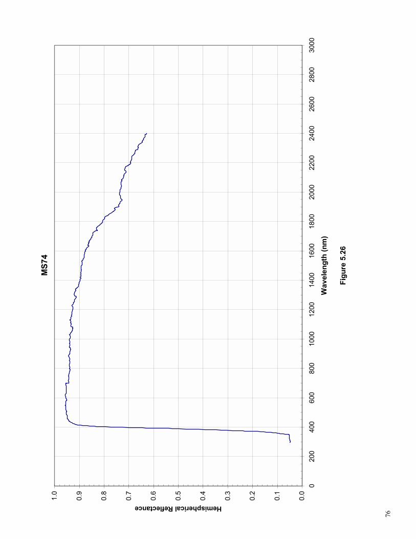
76
MS7
4
0.0
0.1
0.2
0.3
0.4
0.5
0.6
0.7
0.8
0.9
1.0
020
040
060
080
010
0012
0014
0016
0018
0020
0022
0024
0026
0028
0030
00
Wav
elen
gth
(nm
)
Figu
re 5
.26
Hemispherical Reflectance
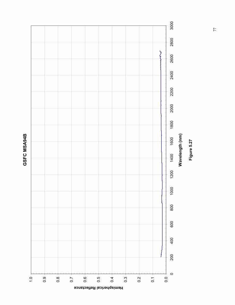
77
GSF
C M
SA94
B
0.0
0.1
0.2
0.3
0.4
0.5
0.6
0.7
0.8
0.9
1.0
020
040
060
080
010
0012
0014
0016
0018
0020
0022
0024
0026
0028
0030
00
Wav
elen
gth
(nm
)
Figu
re 5
.27
Hemispherical Reflectance
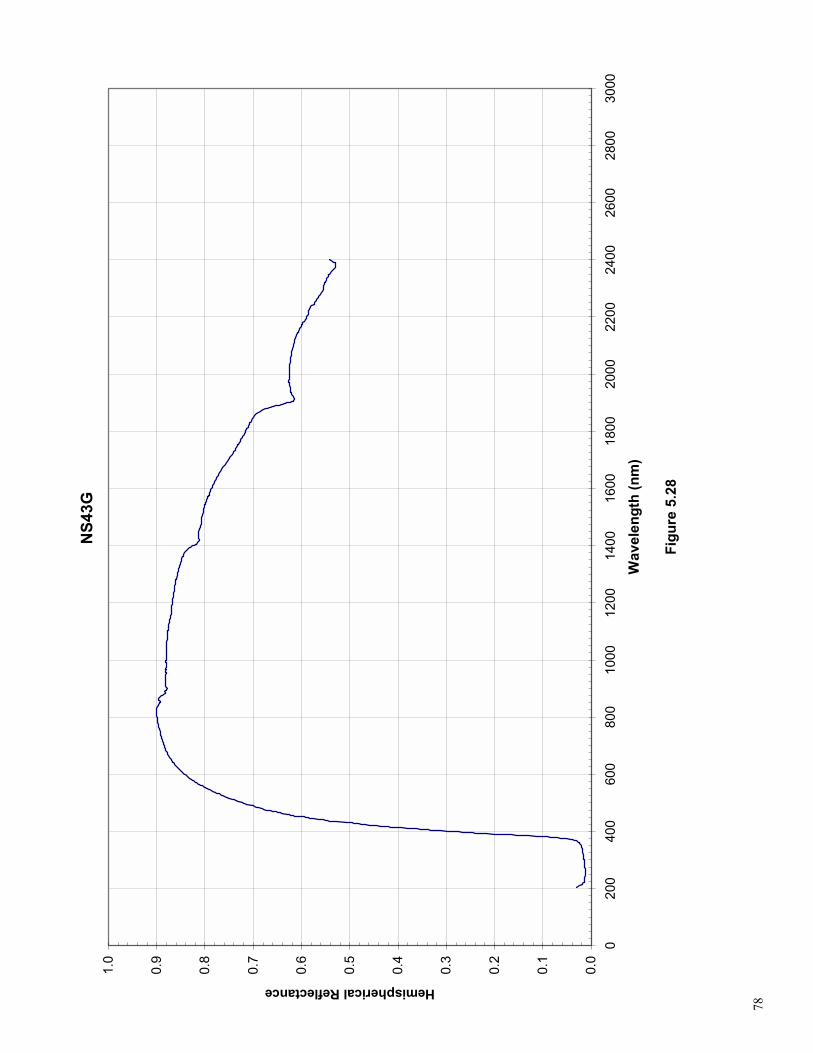
78
NS4
3G
0.0
0.1
0.2
0.3
0.4
0.5
0.6
0.7
0.8
0.9
1.0
020
040
060
080
010
0012
0014
0016
0018
0020
0022
0024
0026
0028
0030
00
Wav
elen
gth
(nm
)
Figu
re 5
.28
Hemispherical Reflectance
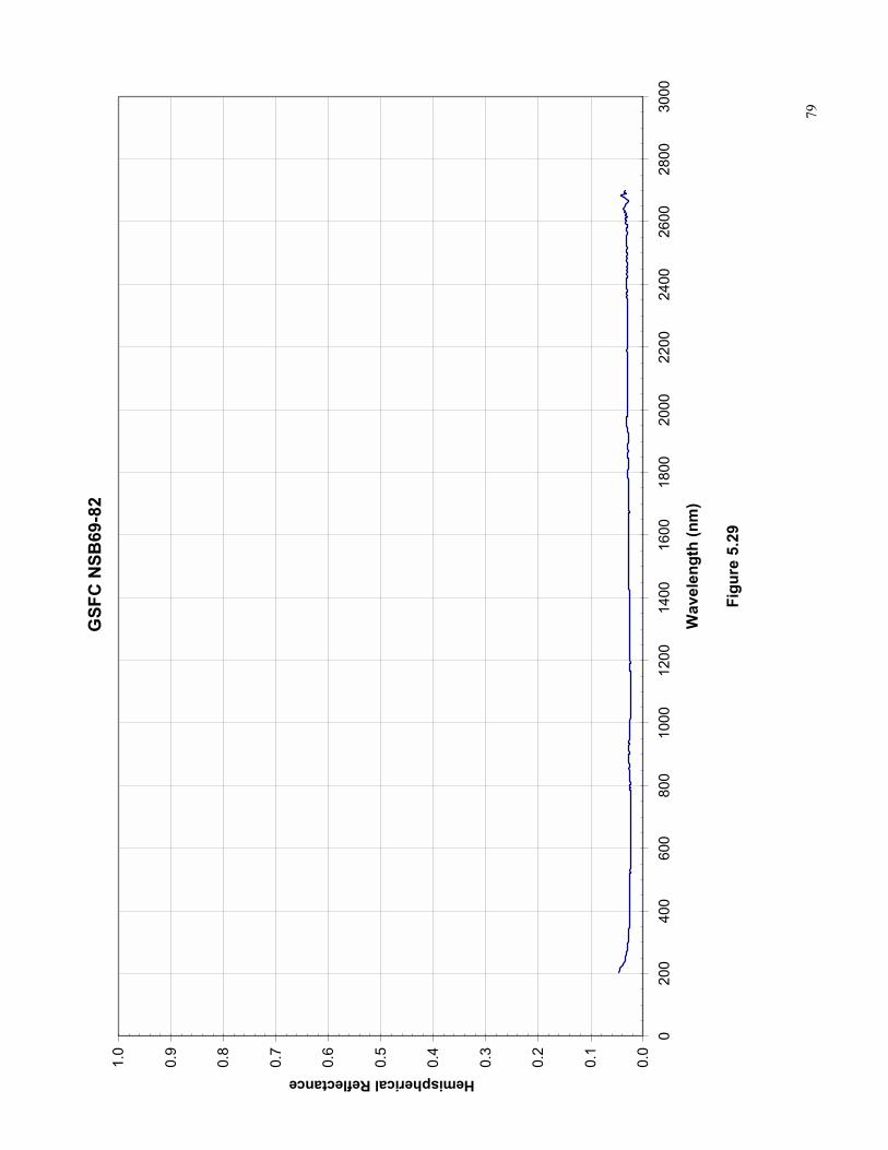
79
GSF
C N
SB69
-82
0.0
0.1
0.2
0.3
0.4
0.5
0.6
0.7
0.8
0.9
1.0
020
040
060
080
010
0012
0014
0016
0018
0020
0022
0024
0026
0028
0030
00
Wav
elen
gth
(nm
)
Figu
re 5
.29
Hemispherical Reflectance
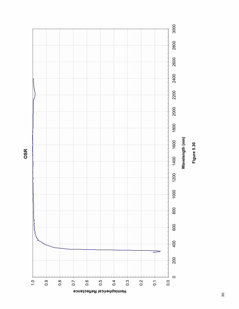
80
OSR
0.0
0.1
0.2
0.3
0.4
0.5
0.6
0.7
0.8
0.9
1.0
020
040
060
080
010
0012
0014
0016
0018
0020
0022
0024
0026
0028
0030
00
Wav
elen
gth
(nm
)
Figu
re 5
.30
Hemispherical Reflectance
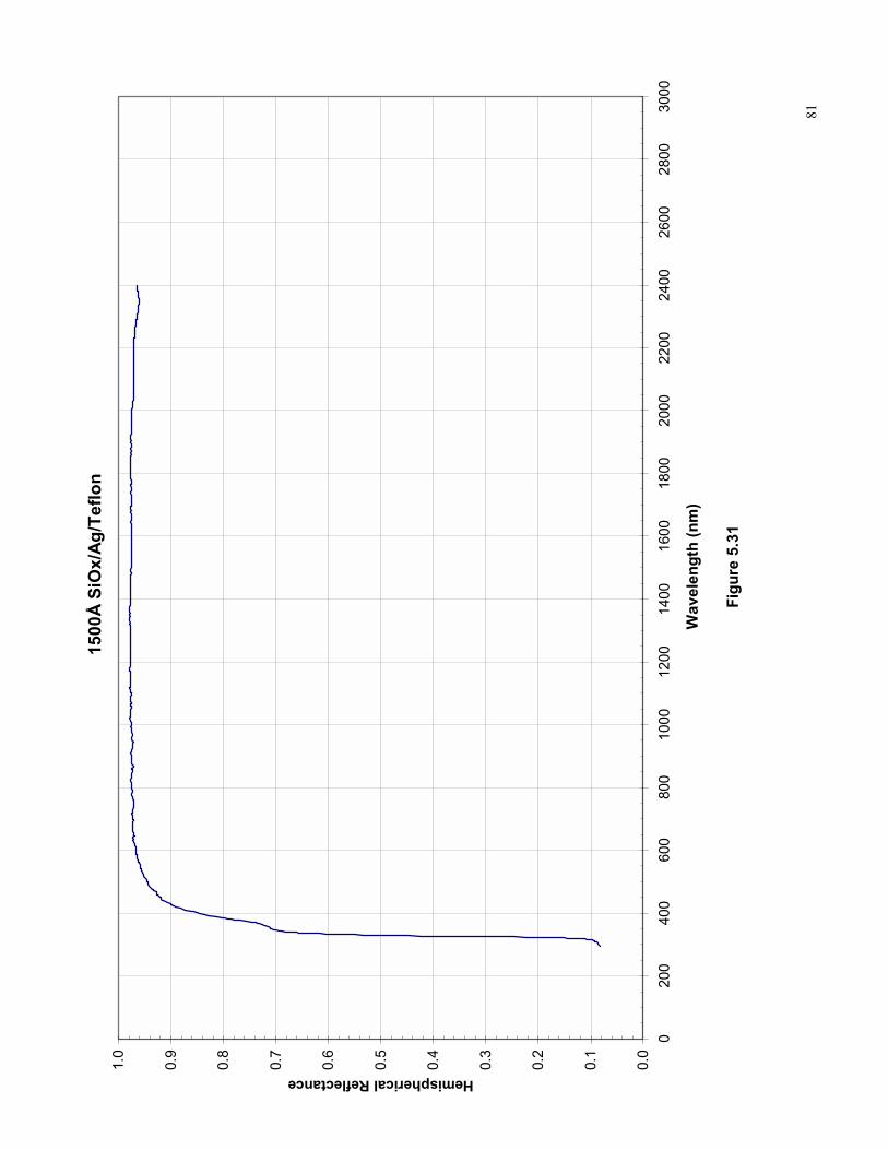
81
1500
Å S
iOx/
Ag/
Teflo
n
0.0
0.1
0.2
0.3
0.4
0.5
0.6
0.7
0.8
0.9
1.0
020
040
060
080
010
0012
0014
0016
0018
0020
0022
0024
0026
0028
0030
00
Wav
elen
gth
(nm
)
Figu
re 5
.31
Hemispherical Reflectance
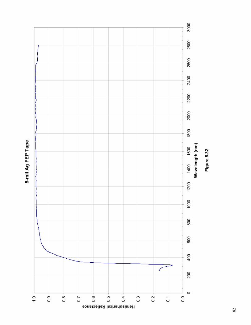
82
5-m
il A
g FE
P Ta
pe
0.0
0.1
0.2
0.3
0.4
0.5
0.6
0.7
0.8
0.9
1.0
020
040
060
080
010
0012
0014
0016
0018
0020
0022
0024
0026
0028
0030
00
Wav
elen
gth
(nm
)
Figu
re 5
.32
Hemispherical Reflectance
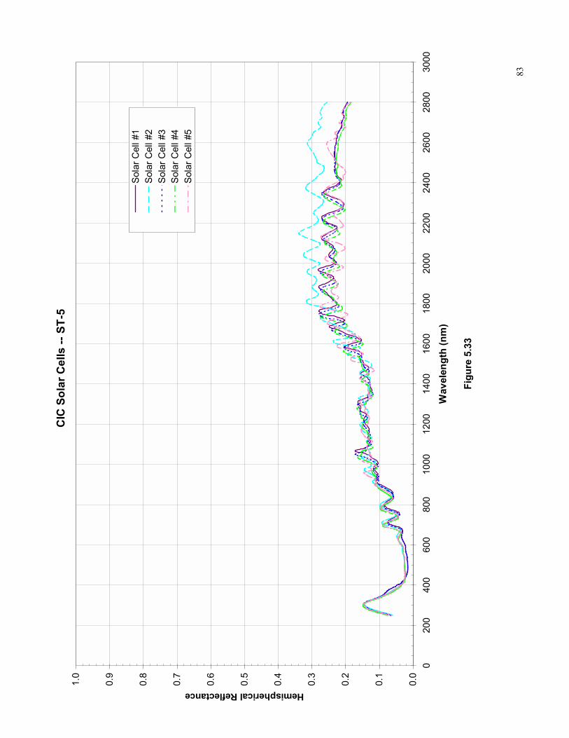
83
CIC
Sol
ar C
ells
-- S
T-5
0.0
0.1
0.2
0.3
0.4
0.5
0.6
0.7
0.8
0.9
1.0
020
040
060
080
010
0012
0014
0016
0018
0020
0022
0024
0026
0028
0030
00
Wav
elen
gth
(nm
)
Figu
re 5
.33
Hemispherical Reflectance
Sol
ar C
ell #
1S
olar
Cel
l #2
Sol
ar C
ell #
3S
olar
Cel
l #4
Sol
ar C
ell #
5
84
HST
SA
III S
olar
Cel
l
0.0
0.1
0.2
0.3
0.4
0.5
0.6
0.7
0.8
0.9
1.0
020
040
060
080
010
0012
0014
0016
0018
0020
0022
0024
0026
0028
0030
00
Wav
elen
gth
(nm
)
Figu
re 5
.34
Hemispherical Reflectance
85
Elec
trop
olis
hed
Stai
nles
s St
eel
0.0
0.1
0.2
0.3
0.4
0.5
0.6
0.7
0.8
0.9
1.0
020
040
060
080
010
0012
0014
0016
0018
0020
0022
0024
0026
0028
0030
00W
avel
engt
h (n
m)
Figu
re 5
.35
Hemispherical Reflectance
Sam
ple
#3
Sam
ple
#5
Sam
ple
#6
86
SiO
x/VD
A/S
tain
less
Ste
el F
oil
0.0
0.1
0.2
0.3
0.4
0.5
0.6
0.7
0.8
0.9
1.0
020
040
060
080
010
0012
0014
0016
0018
0020
0022
0024
0026
0028
0030
00
Wav
elen
gth
(nm
)
Figu
re 5
.36
Hemispherical Emittance
87
SiO
x/Te
dlar
1.5
mils
0.0
0.1
0.2
0.3
0.4
0.5
0.6
0.7
0.8
0.9
1.0
020
040
060
080
010
0012
0014
0016
0018
0020
0022
0024
0026
0028
0030
00
Wav
leng
th (n
m)
Figu
re 5
.37
Hemispherical Emittance
88
VDA
/Lac
quer
0.0
0.1
0.2
0.3
0.4
0.5
0.6
0.7
0.8
0.9
1.0
020
040
060
080
010
0012
0014
0016
0018
0020
0022
0024
0026
0028
0030
00W
avel
engt
h (n
m)
Figu
re 5
.38
Hemispherical Reflectance
VD
A/L
acqu
erV
DA
/Abr
aide
d La
cque
r
89
YB71
0.0
0.1
0.2
0.3
0.4
0.5
0.6
0.7
0.8
0.9
1.0
020
040
060
080
010
0012
0014
0016
0018
0020
0022
0024
0026
0028
0030
00
Wav
elen
gth
(nm
)
Figu
re 5
.39
Hemipherical Emittance

90
VI. Total Hemispherical Emittance as a Function of Temperature For Selected Thermal Control Coatings
The emittance measurements that follow were determined by a calorimetric technique as described in section 3.2.3. The thickness of each coating has been noted in parentheses on each chart and all coatings were on an Aluminum substrate unless otherwise noted. It is important to note that the emittance of each coating is a function of thickness, if a different coating thickness is used the resulting emittance as a function of temperature may be somewhat different. These tests represent data collected over a 10-year period by Lonny Kauder.
91
Aero
glaz
e A2
76 (3
.0 m
ils)
0.0
0.1
0.2
0.3
0.4
0.5
0.6
0.7
0.8
0.9
1.0
025
5075
100
125
150
175
200
225
250
275
300
325
350
375
400
Tem
pera
ture
(°K
)
Figu
re 6
.1
Hemispherical Emittance
92
Che
mgl
aze
Z202
(1.6
mils
)
0.0
0.1
0.2
0.3
0.4
0.5
0.6
0.7
0.8
0.9
1.0
025
5075
100
125
150
175
200
225
250
275
300
325
350
375
400
Tem
pera
ture
(°K
)
Figu
re 6
.2
Hemispherical Emittance
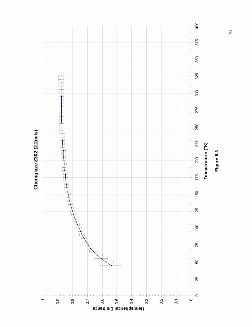
93
Che
mgl
aze
Z302
(2.2
mils
)
0
0.1
0.2
0.3
0.4
0.5
0.6
0.7
0.8
0.91
025
5075
100
125
150
175
200
225
250
275
300
325
350
375
400
Tem
pera
ture
(°K
)
Figu
re 6
.3
Hemispherical Emittance
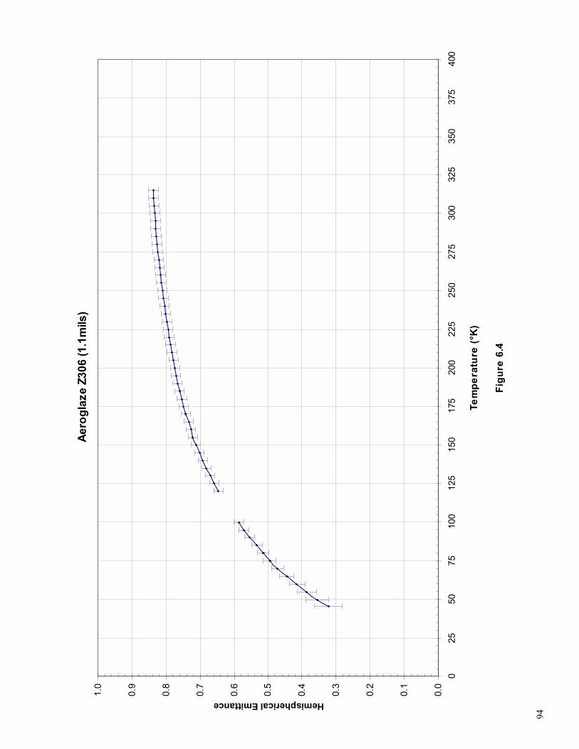
94
Aero
glaz
e Z3
06 (1
.1m
ils)
0.0
0.1
0.2
0.3
0.4
0.5
0.6
0.7
0.8
0.9
1.0
025
5075
100
125
150
175
200
225
250
275
300
325
350
375
400
Tem
pera
ture
(°K
)
Figu
re 6
.4
Hemispherical Emittance
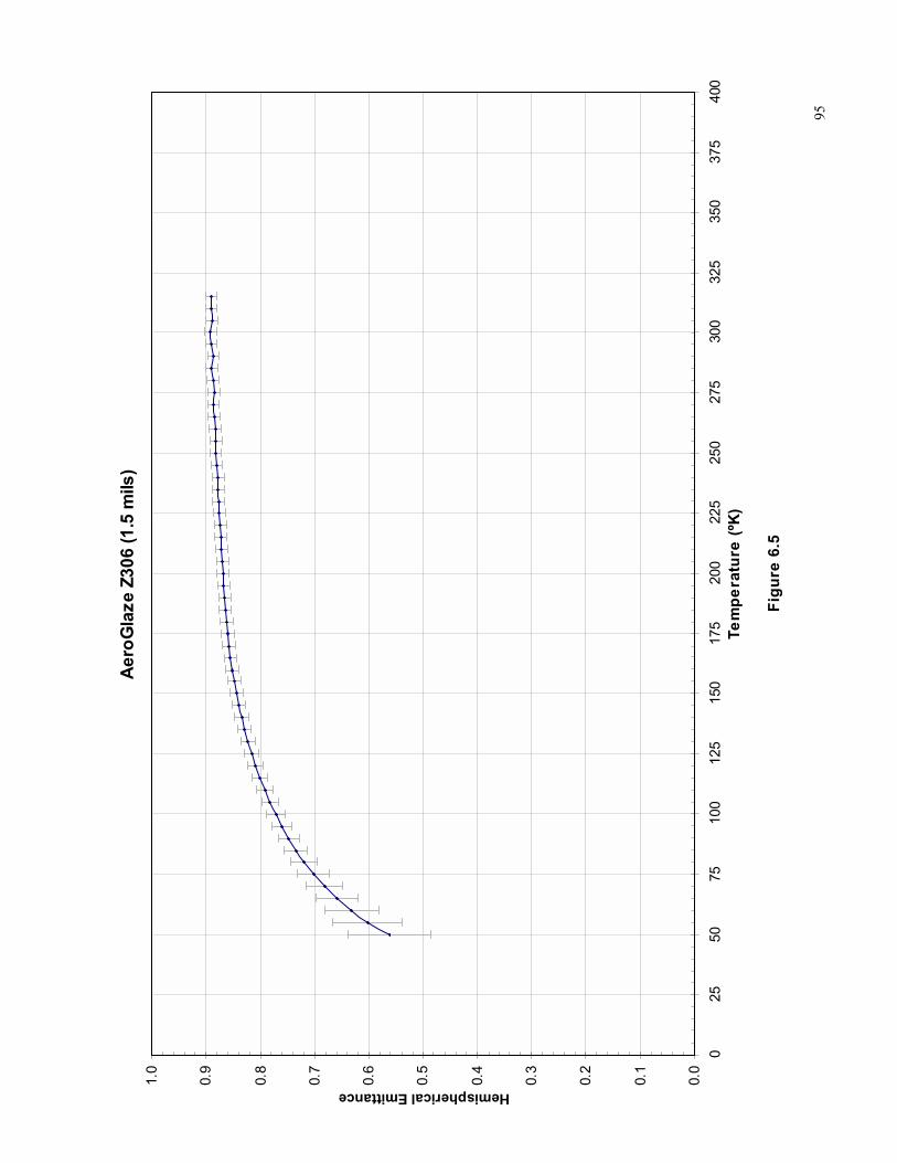
95
Aer
oGla
ze Z
306
(1.5
mils
)
0.0
0.1
0.2
0.3
0.4
0.5
0.6
0.7
0.8
0.9
1.0
025
5075
100
125
150
175
200
225
250
275
300
325
350
375
400
Tem
pera
ture
(ºK
)
Figu
re 6
.5
Hemispherical Emittance
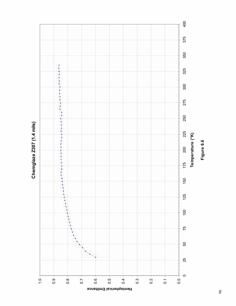
96
Che
mgl
aze
Z307
(1.4
mils
)
0.0
0.1
0.2
0.3
0.4
0.5
0.6
0.7
0.8
0.9
1.0
025
5075
100
125
150
175
200
225
250
275
300
325
350
375
400
Tem
pera
ture
(°K
)
Figu
re 6
.6
Hemispherical Emittance
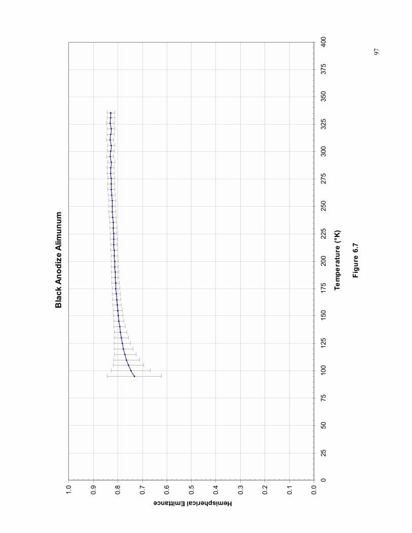
97
Bla
ck A
nodi
ze A
limun
um
0.0
0.1
0.2
0.3
0.4
0.5
0.6
0.7
0.8
0.9
1.0
025
5075
100
125
150
175
200
225
250
275
300
325
350
375
400
Tem
pera
ture
(°K
)
Figu
re 6
.7
Hemispherical Emittance
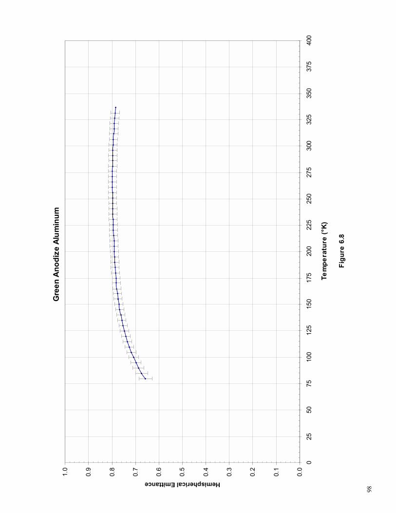
98
Gre
en A
nodi
ze A
lum
inum
0.0
0.1
0.2
0.3
0.4
0.5
0.6
0.7
0.8
0.9
1.0
025
5075
100
125
150
175
200
225
250
275
300
325
350
375
400
Tem
pera
ture
(°K
)
Figu
re 6
.8
Hemispherical Emittance
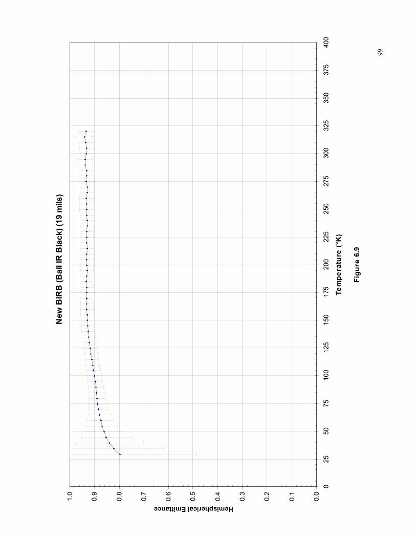
99
New
BIR
B (B
all I
R B
lack
) (19
mils
)
0.0
0.1
0.2
0.3
0.4
0.5
0.6
0.7
0.8
0.9
1.0
025
5075
100
125
150
175
200
225
250
275
300
325
350
375
400
Tem
pera
ture
(°K
)
Figu
re 6
.9
Hemispherical Emittance
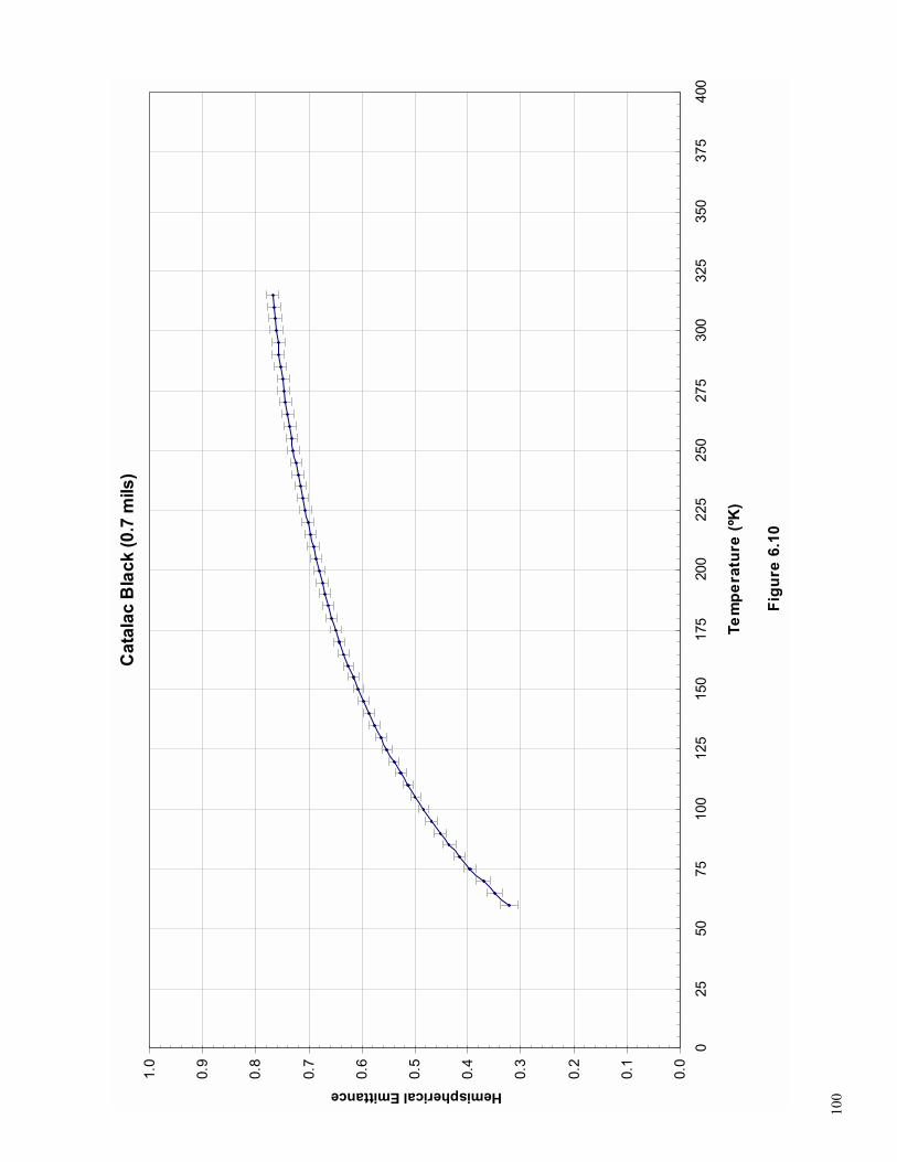
100
Cat
alac
Bla
ck (0
.7 m
ils)
0.0
0.1
0.2
0.3
0.4
0.5
0.6
0.7
0.8
0.9
1.0
025
5075
100
125
150
175
200
225
250
275
300
325
350
375
400
Tem
pera
ture
(ºK
)
Figu
re 6
.10
Hemispherical Emittance
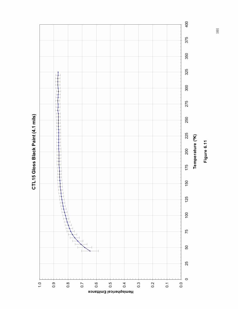
10
1
CTL
15 G
loss
Bla
ck P
aint
(4.1
mils
)
0.0
0.1
0.2
0.3
0.4
0.5
0.6
0.7
0.8
0.9
1.0
025
5075
100
125
150
175
200
225
250
275
300
325
350
375
400
Tem
pera
ture
(ºK
)
Figu
re 6
.11
Hemispherical Emittance
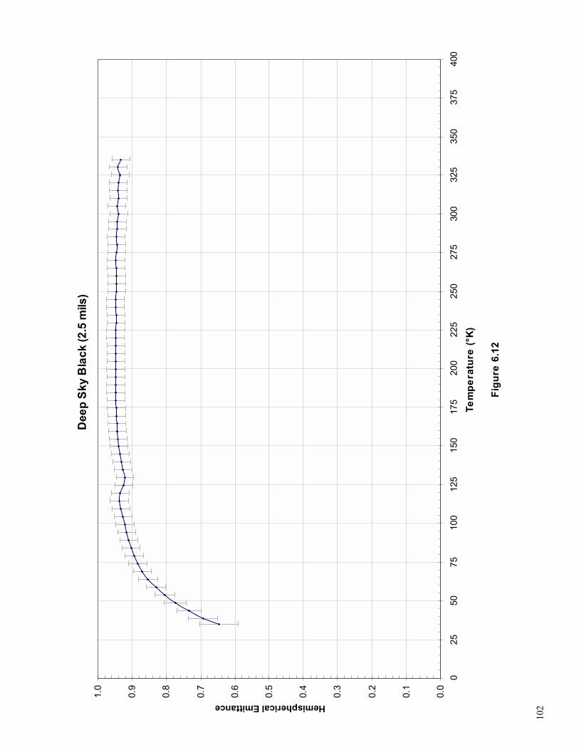
102
Dee
p S
ky B
lack
(2.5
mils
)
0.0
0.1
0.2
0.3
0.4
0.5
0.6
0.7
0.8
0.9
1.0
025
5075
100
125
150
175
200
225
250
275
300
325
350
375
400
Tem
pera
ture
(°K
)
Figu
re 6
.12
Hemispherical Emittance
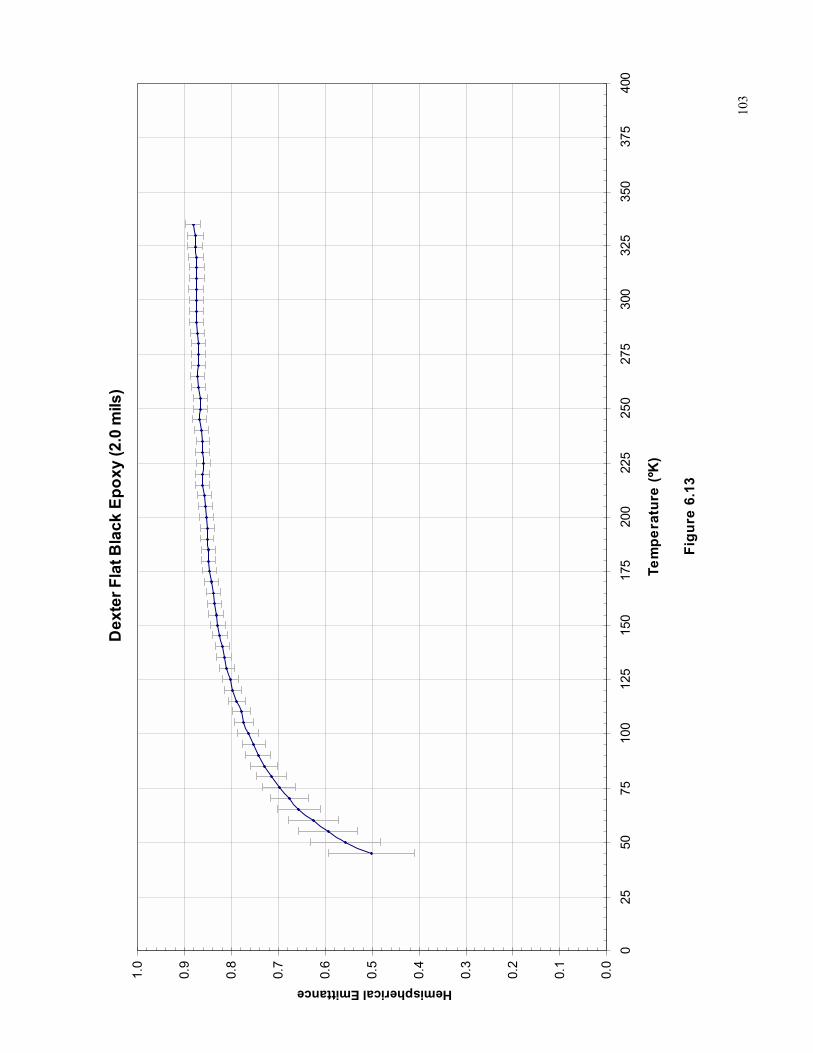
10
3
Dex
ter F
lat B
lack
Epo
xy (2
.0 m
ils)
0.0
0.1
0.2
0.3
0.4
0.5
0.6
0.7
0.8
0.9
1.0
025
5075
100
125
150
175
200
225
250
275
300
325
350
375
400
Tem
pera
ture
(ºK
)
Figu
re 6
.13
Hemispherical Emittance
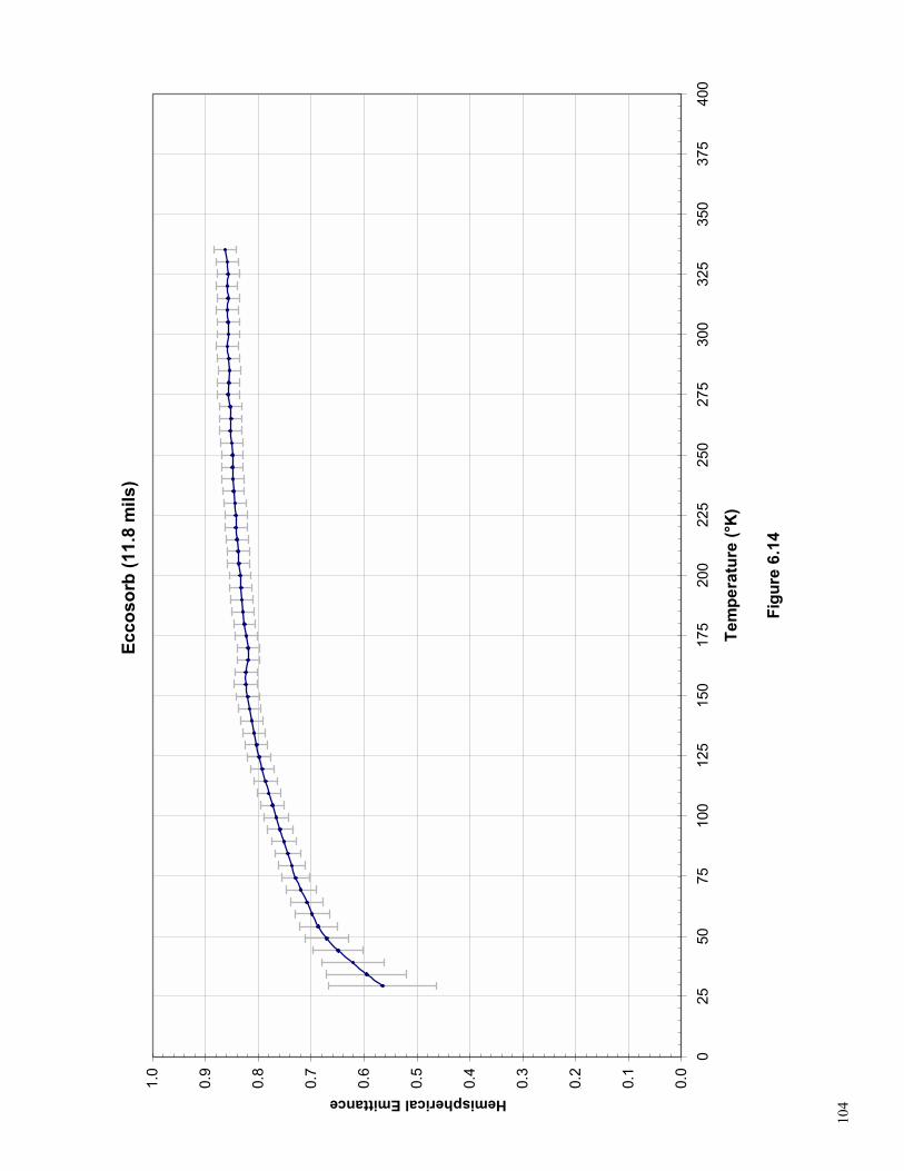
104
Ecco
sorb
(11.
8 m
ils)
0.0
0.1
0.2
0.3
0.4
0.5
0.6
0.7
0.8
0.9
1.0
025
5075
100
125
150
175
200
225
250
275
300
325
350
375
400
Tem
pera
ture
(°K
)
Figu
re 6
.14
Hemispherical Emittance
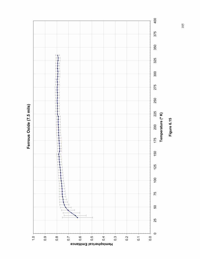
10
5
Ferr
ous
Oxi
de (7
.5 m
ils)
0.0
0.1
0.2
0.3
0.4
0.5
0.6
0.7
0.8
0.9
1.0
025
5075
100
125
150
175
200
225
250
275
300
325
350
375
400
Tem
pera
ture
(º K
)
Figu
re 6
.15
Hemispherical Emittance
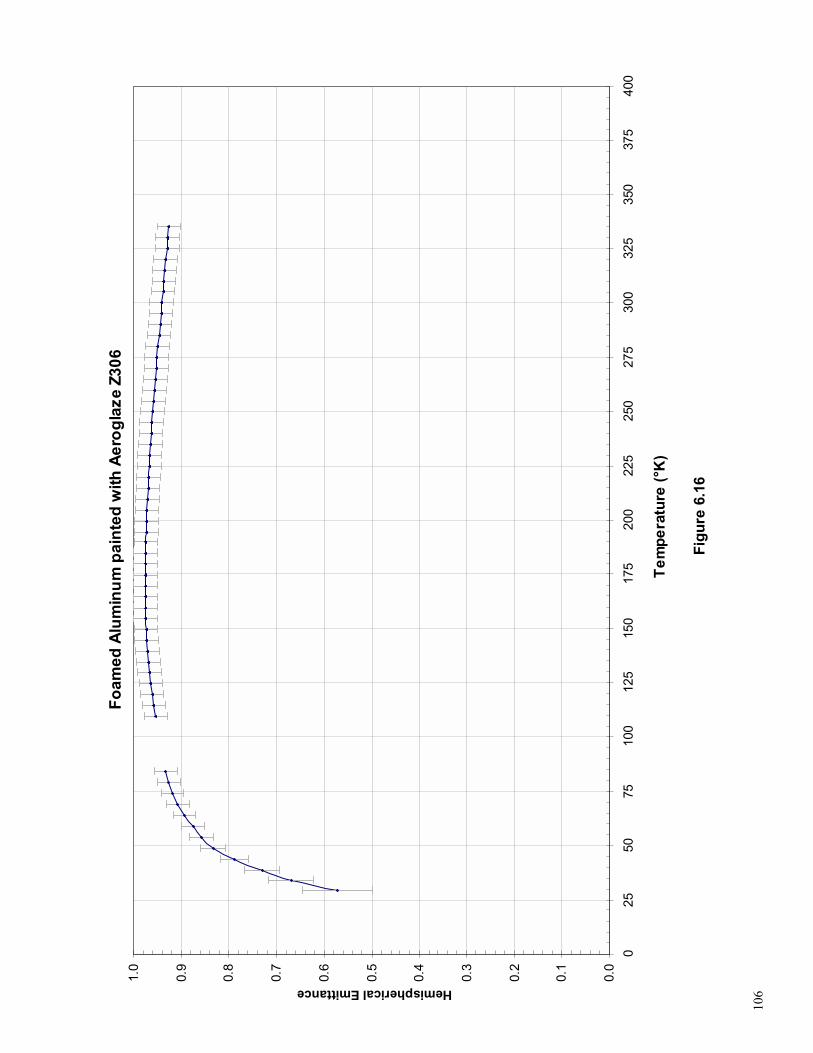
106
Foam
ed A
lum
inum
pai
nted
with
Aer
ogla
ze Z
306
0.0
0.1
0.2
0.3
0.4
0.5
0.6
0.7
0.8
0.9
1.0
025
5075
100
125
150
175
200
225
250
275
300
325
350
375
400
Tem
pera
ture
(°K
)
Figu
re 6
.16
Hemispherical Emittance
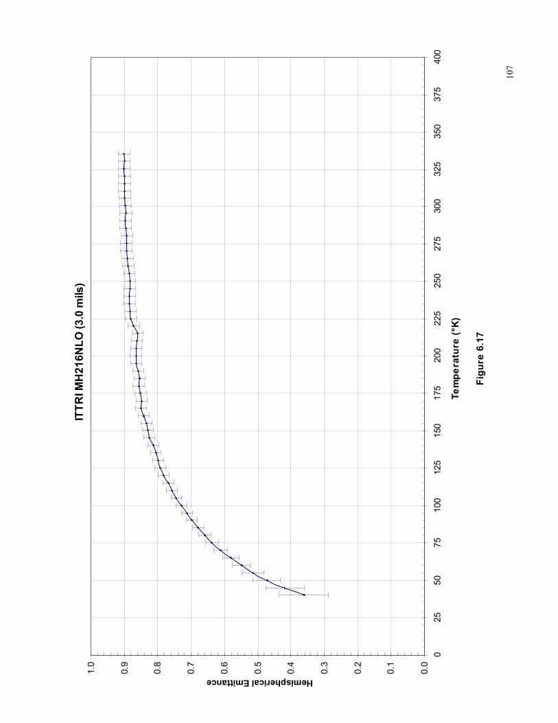
10
7
ITTR
I MH
216N
LO (3
.0 m
ils)
0.0
0.1
0.2
0.3
0.4
0.5
0.6
0.7
0.8
0.9
1.0
025
5075
100
125
150
175
200
225
250
275
300
325
350
375
400
Tem
pera
ture
(°K
)
Figu
re 6
.17
Hemispherical Emittance
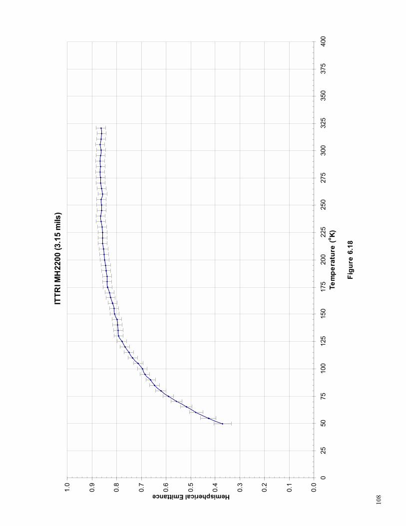
108
ITTR
I MH
2200
(3.1
5 m
ils)
0.0
0.1
0.2
0.3
0.4
0.5
0.6
0.7
0.8
0.9
1.0
025
5075
100
125
150
175
200
225
250
275
300
325
350
375
400
Tem
pera
ture
(o K)
Figu
re 6
.18
Hemispherical Emittance
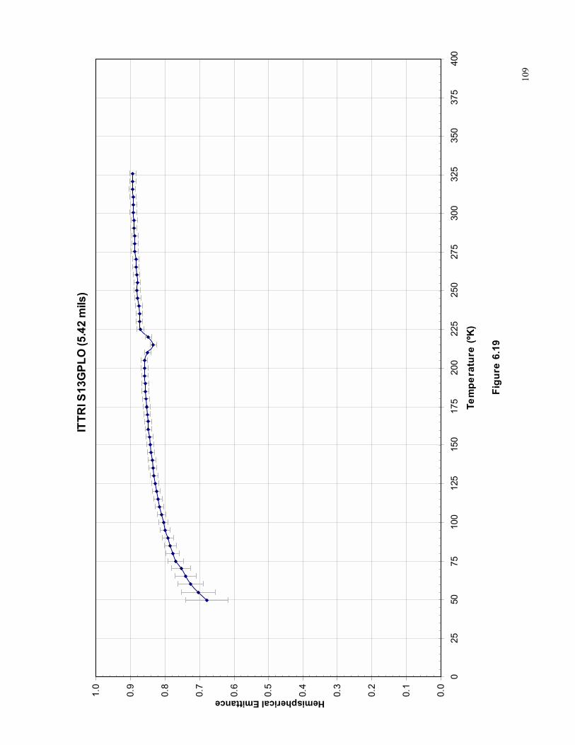
10
9
ITTR
I S13
GPL
O (5
.42
mils
)
0.0
0.1
0.2
0.3
0.4
0.5
0.6
0.7
0.8
0.9
1.0
025
5075
100
125
150
175
200
225
250
275
300
325
350
375
400
Tem
pera
ture
(ºK
)
Figu
re 6
.19
Hemispherical Emittance
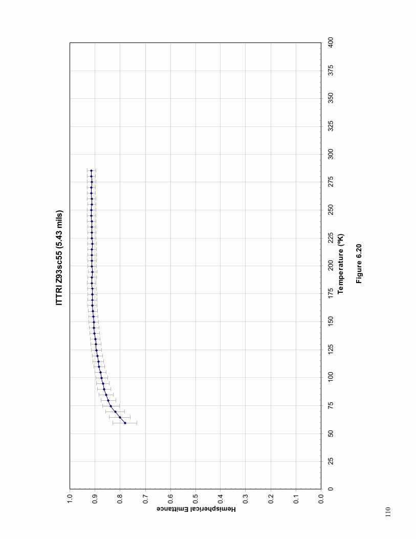
110
ITTR
I Z93
sc55
(5.4
3 m
ils)
0.0
0.1
0.2
0.3
0.4
0.5
0.6
0.7
0.8
0.9
1.0
025
5075
100
125
150
175
200
225
250
275
300
325
350
375
400
Tem
pera
ture
(ºK
)
Figu
re 6
.20
Hemispherical Emittance
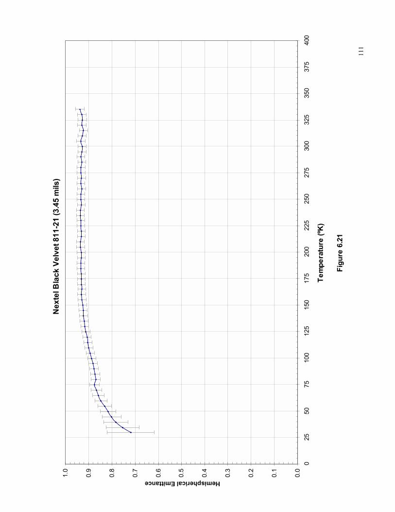
11
1
Nex
tel B
lack
Vel
vet 8
11-2
1 (3
.45
mils
)
0.0
0.1
0.2
0.3
0.4
0.5
0.6
0.7
0.8
0.9
1.0
025
5075
100
125
150
175
200
225
250
275
300
325
350
375
400
Tem
pera
ture
(ºK
)
Figu
re 6
.21
Hemispherical Emittance
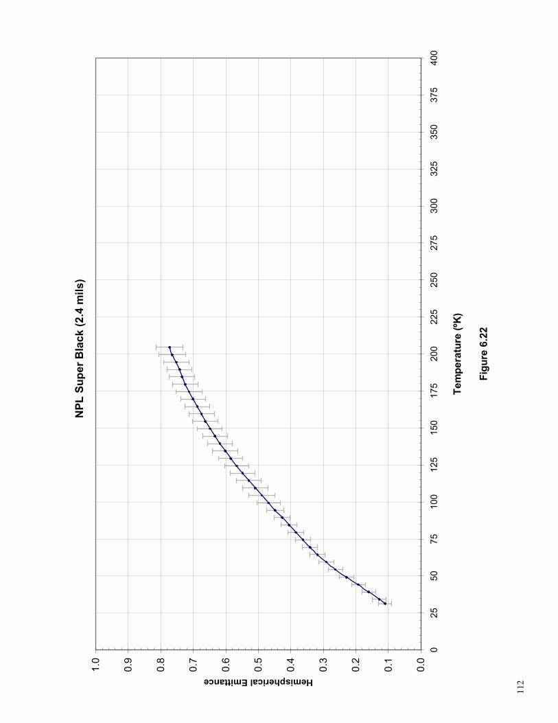
112
NPL
Sup
er B
lack
(2.4
mils
)
0.0
0.1
0.2
0.3
0.4
0.5
0.6
0.7
0.8
0.9
1.0
025
5075
100
125
150
175
200
225
250
275
300
325
350
375
400
Tem
pera
ture
(ºK
)
Figu
re 6
.22
Hemispherical Emittance
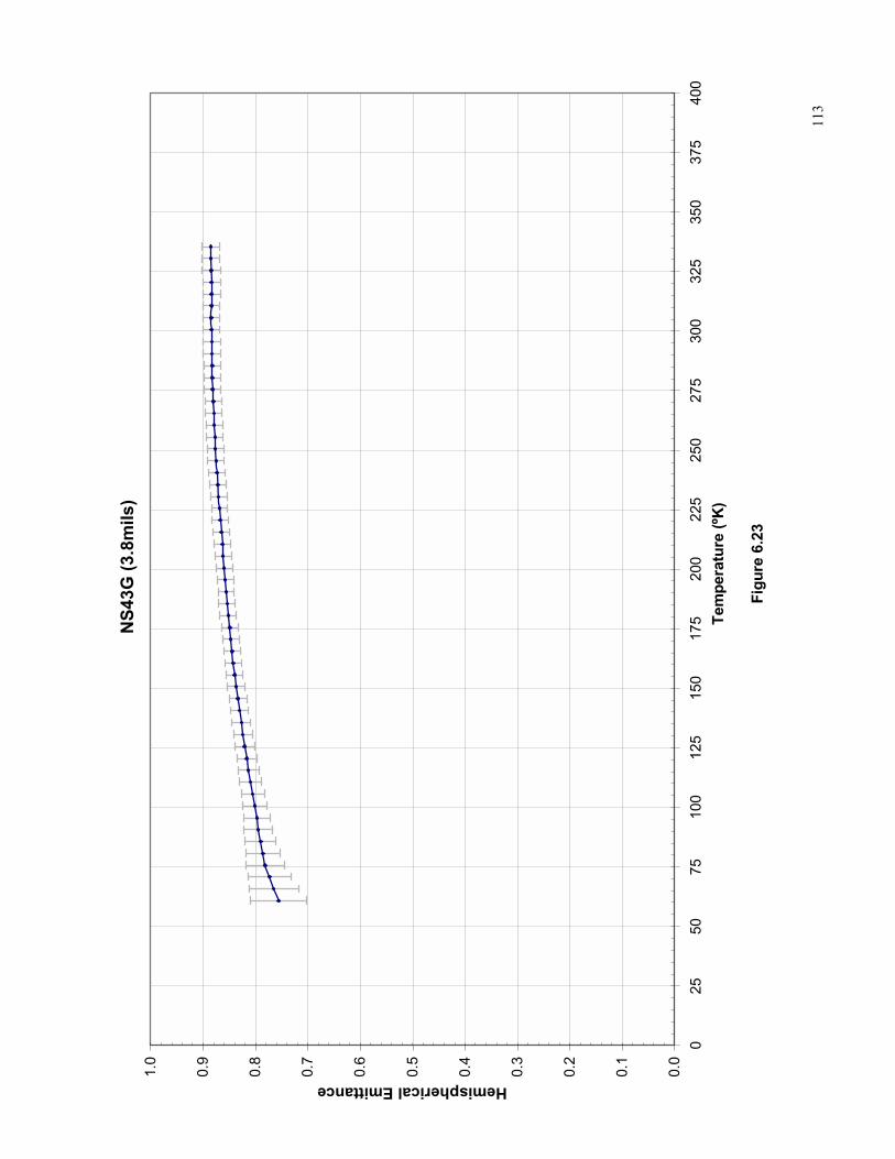
11
3
NS4
3G (3
.8m
ils)
0.0
0.1
0.2
0.3
0.4
0.5
0.6
0.7
0.8
0.9
1.0
025
5075
100
125
150
175
200
225
250
275
300
325
350
375
400
Tem
pera
ture
(ºK
)
Figu
re 6
.23
Hemispherical Emittance
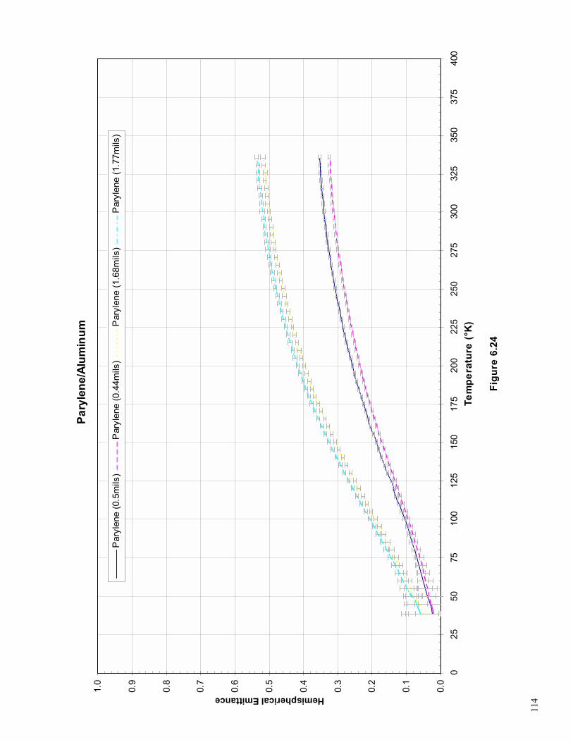
114
Par
ylen
e/Al
umin
um
0.0
0.1
0.2
0.3
0.4
0.5
0.6
0.7
0.8
0.9
1.0
025
5075
100
125
150
175
200
225
250
275
300
325
350
375
400
Tem
pera
ture
(°K
)
Figu
re 6
.24
Hemispherical Emittance
Par
ylen
e (0
.5m
ils)
Par
ylen
e (0
.44m
ils)
Par
ylen
e (1
.68m
ils)
Par
ylen
e (1
.77m
ils)
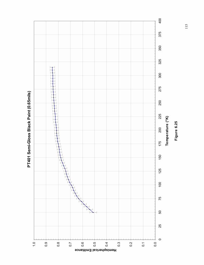
11
5
PT4
01 S
emi-G
loss
Bla
ck P
aint
(0.6
5mils
)
0.0
0.1
0.2
0.3
0.4
0.5
0.6
0.7
0.8
0.9
1.0
025
5075
100
125
150
175
200
225
250
275
300
325
350
375
400
Tem
pera
ture
(°K
)
Figu
re 6
.25
Hemispherical Emittance
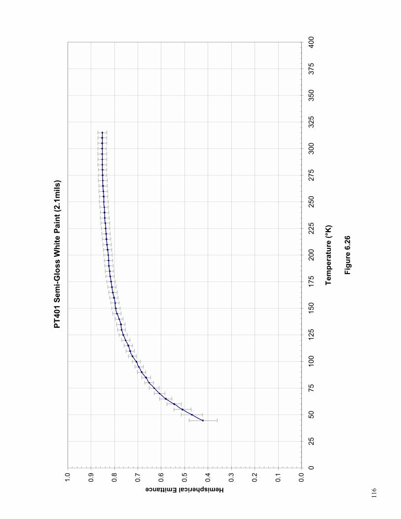
116
PT40
1 Se
mi-G
loss
Whi
te P
aint
(2.1
mils
)
0.0
0.1
0.2
0.3
0.4
0.5
0.6
0.7
0.8
0.9
1.0
025
5075
100
125
150
175
200
225
250
275
300
325
350
375
400
Tem
pera
ture
(°K
)
Figu
re 6
.26
Hemispherical Emittance
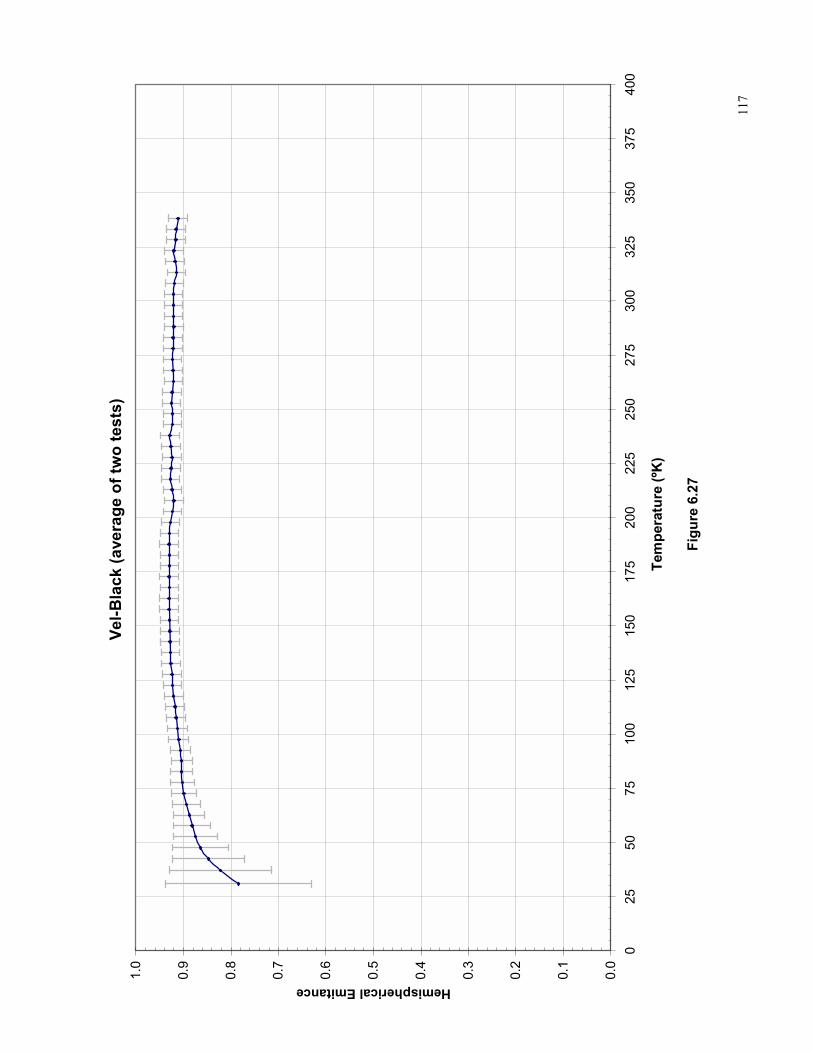
11
7
Vel-B
lack
(ave
rage
of t
wo
test
s)
0.0
0.1
0.2
0.3
0.4
0.5
0.6
0.7
0.8
0.9
1.0
025
5075
100
125
150
175
200
225
250
275
300
325
350
375
400
Tem
pera
ture
(ºK
)
Figu
re 6
.27
Hemispherical Emitance
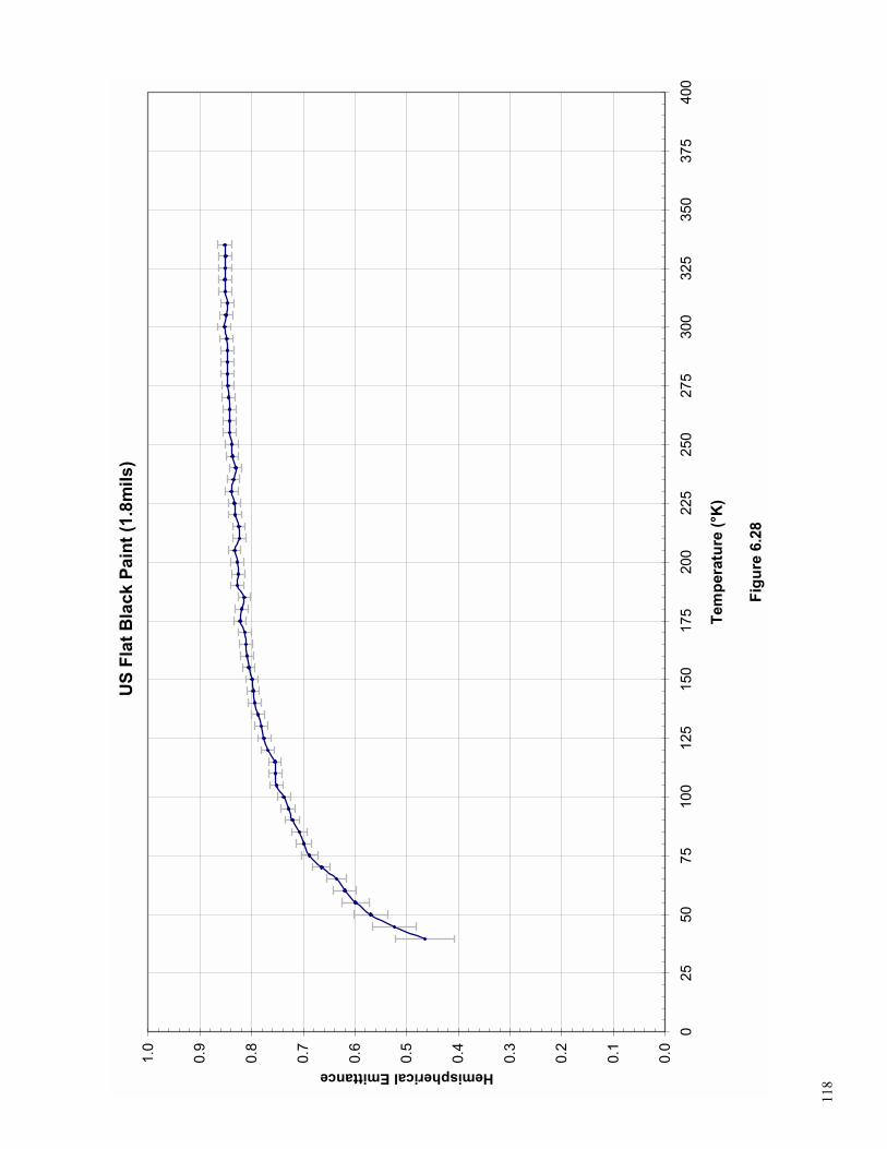
118
US
Flat
Bla
ck P
aint
(1.8
mils
)
0.0
0.1
0.2
0.3
0.4
0.5
0.6
0.7
0.8
0.9
1.0
025
5075
100
125
150
175
200
225
250
275
300
325
350
375
400
Tem
pera
ture
(°K
)
Figu
re 6
.28
Hemispherical Emittance
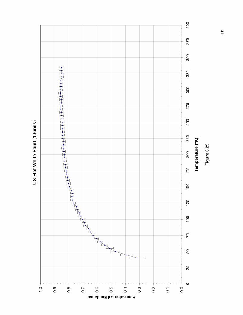
11
9
US
Flat
Whi
te P
aint
(1.6
mils
)
0.0
0.1
0.2
0.3
0.4
0.5
0.6
0.7
0.8
0.9
1.0
025
5075
100
125
150
175
200
225
250
275
300
325
350
375
400
Tem
pera
ture
(°K
)
Figu
re 6
.29
Hemispherical Emittance
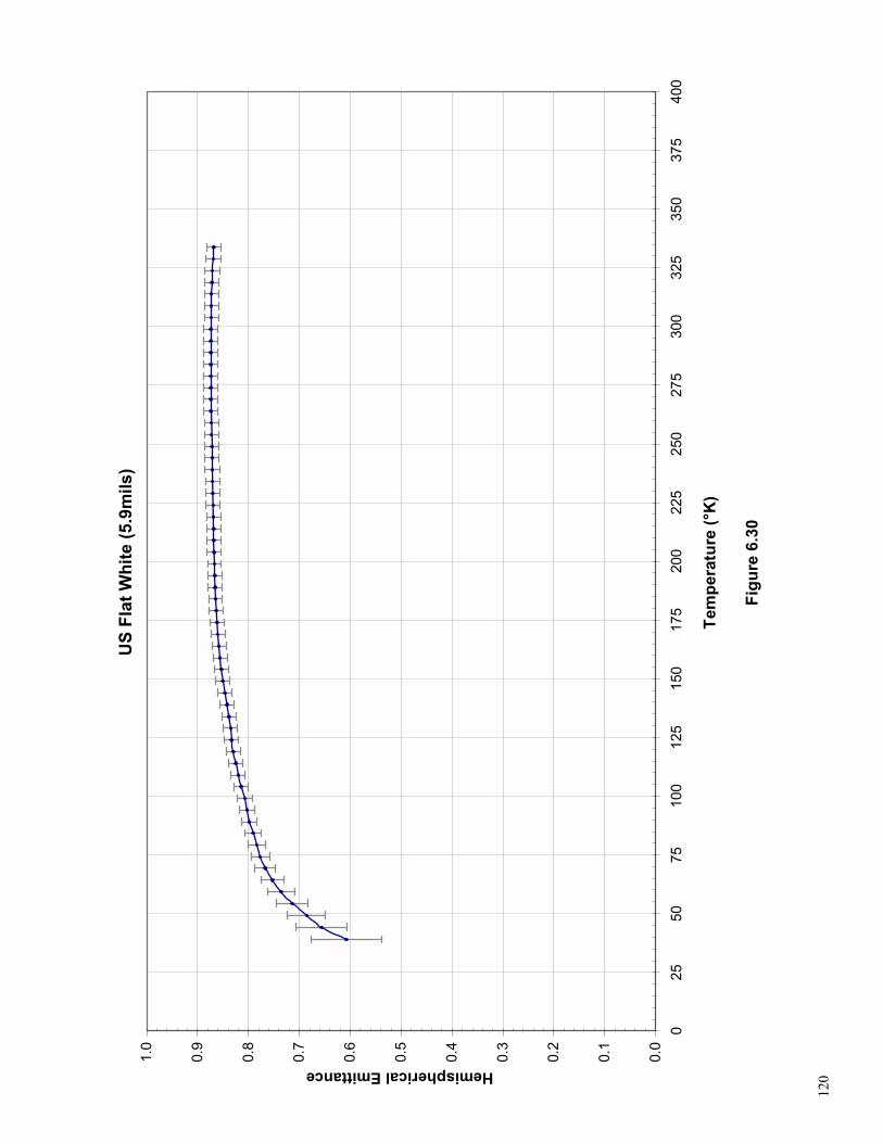
120
US
Flat
Whi
te (5
.9m
ils)
0.0
0.1
0.2
0.3
0.4
0.5
0.6
0.7
0.8
0.9
1.0
025
5075
100
125
150
175
200
225
250
275
300
325
350
375
400
Tem
pera
ture
(°K
)
Figu
re 6
.30
Hemispherical Emittance
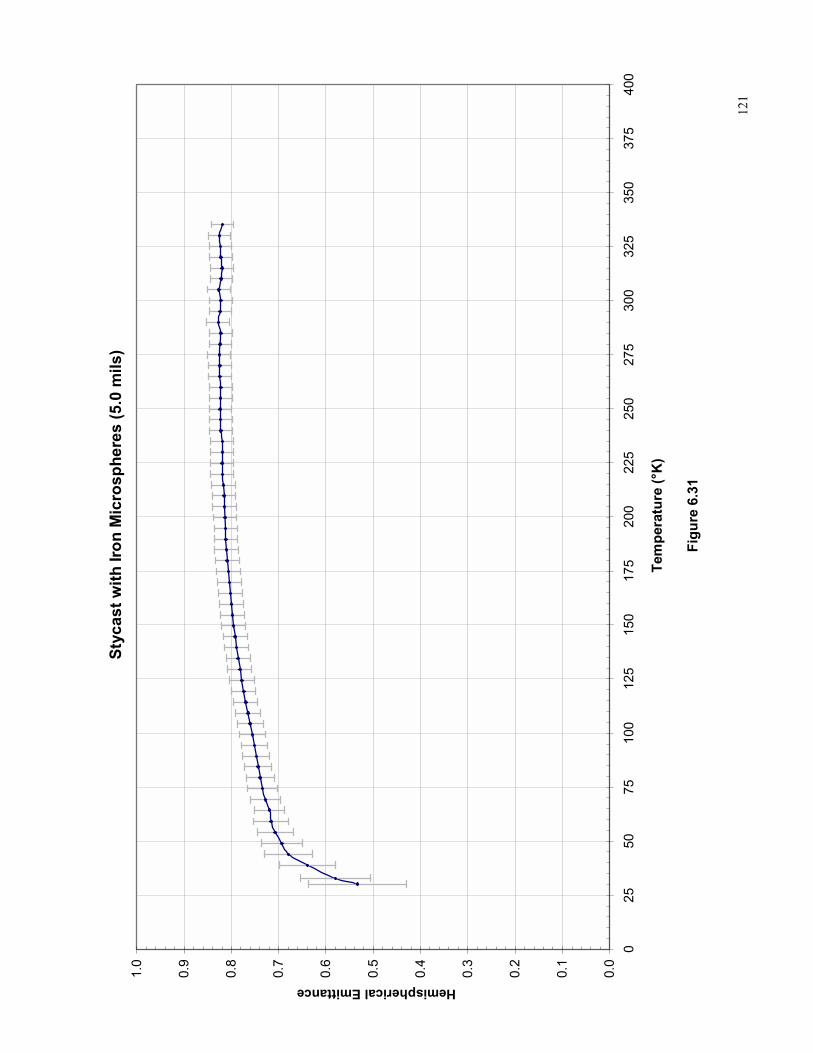
12
1
Styc
ast w
ith Ir
on M
icro
sphe
res
(5.0
mils
)
0.0
0.1
0.2
0.3
0.4
0.5
0.6
0.7
0.8
0.9
1.0
025
5075
100
125
150
175
200
225
250
275
300
325
350
375
400
Tem
pera
ture
(°K
)
Figu
re 6
.31
Hemispherical Emittance
REPORT DOCUMENTATION PAGE Form Approved OMB No. 0704-0188
The public reporting burden for this collection of information is estimated to average 1 hour per response, including the time for reviewing instructions, searching existingdata sources, gathering and maintaining the data needed, and completing and reviewing the collection of information. Send comments regarding this burden estimate or any other aspect of this collection of information, including suggestions for reducing this burden, to Department of Defense, Washington Headquarters Services, Directorate for Information Operations and Reports (0704-0188), 1215 Jefferson Davis Highway, Suite 1204, Arlington, VA 22202-4302. Respondents should be aware that notwithstanding any other provision of law, no person shall be subject to any penalty for failing to comply with a collection of information if it does not display a currently valid OMB control number. PLEASE DO NOT RETURN YOUR FORM TO THE ABOVE ADDRESS. 1. REPORT DATE (DD-MM-YYYY) 2. REPORT TYPE 3. DATES COVERED (From - To)
4. TITLE AND SUBTITLE 5a. CONTRACT NUMBER
5b. GRANT NUMBER
5c. PROGRAM ELEMENT NUMBER
6. AUTHOR(S) 5d. PROJECT NUMBER
5e. TASK NUMBER
5f. WORK UNIT NUMBER
7. PERFORMING ORGANIZATION NAME(S) AND ADDRESS(ES) 8. PERFORMING ORGANIZATION REPORT NUMBER
9. SPONSORING/MONITORING AGENCY NAME(S) AND ADDRESS(ES) 10. SPONSORING/MONITOR'S ACRONYM(S)
11. SPONSORING/MONITORINGREPORT NUMBER
12. DISTRIBUTION/AVAILABILITY STATEMENT
13. SUPPLEMENTARY NOTES
14. ABSTRACT
15. SUBJECT TERMS
16. SECURITY CLASSIFICATION OF: 17. LIMITATION OF ABSTRACT
18. NUMBER OF PAGES
19b. NAME OF RESPONSIBLE PERSON
a. REPORT b. ABSTRACT c. THIS PAGE 19b. TELEPHONE NUMBER (Include area code)
Standard Form 298 (Rev. 8-98)Prescribed by ANSI Std. Z39-18


![Spacecraft Simulation]](https://img.pdfslide.us/doc/110x75/544e0a73b1af9f33638b4bf0/spacecraft-simulation.jpg)
