Embed Size (px)
Citation preview
WP365 (v1.2) July 30, 2012 www.xilinx.com 1
© 2010–2012 Xilinx, Inc. Xilinx, the Xilinx logo, Artix, ISE, Kintex, Spartan, Virtex, Vivado, Zynq, and other designated brands included herein are trademarks of Xilinx in the United States and other countries. All other trademarks are the property of their respective owners.
While design security is often thought of in terms ofprotecting intellectual property (IP), the potentiallosses extend beyond just the financial. With theexpansion of the use of programmable logic beyondcommercial markets to avionic and militaryapplications, design security takes on the additionalaspects of safety and national security.
Solutions for protecting application data duringtransmission and storage are well known, but muchless attention has been paid to FPGA designsecurity—that is, protecting the FPGA configurationdata.
This white paper describes the various threats todesign security and the solutions offered by modernFPGAs.
White Paper: FPGAs
WP365 (v1.2) July 30, 2012
Solving Today's Design Security Concerns
By: Steven McNeil

2 www.xilinx.com WP365 (v1.2) July 30, 2012
Introduction
IntroductionToday's global marketplace has opened up not only new opportunities but new threats as well. These threats range from counterfeiting to espionage and are faced by corporations and governments alike. These threats can have far-reaching consequences well beyond the financial well-being of a corporation; they can also impact personal safety.
The goals of those making these threats can range from purely financial—a simple desire to reap profits without making the investment in the initial design effort—to more sinister aspects of governments attempting both to learn the capabilities of others’ systems and to use the knowledge gained to kick-start their own development projects. Given their growing sophistication, there is also the potential of terrorists attempting to exploit weaknesses in design security.
With our global market, commercial products can be obtained easily, either by legitimate means or simply by theft. Military devices can be obtained through espionage, by the capture of equipment on the battlefield, or even when smart ordinance fails to detonate. This ease of access means that everyone must take design security seriously.
Moreover, with the ever-expanding usage of FPGAs in products and systems of all kinds, FPGAs often form the core of any system. This rise in both the usage and importance of FPGAs in a system make protecting the IP contained in FPGAs as important as protecting the data processed by the FPGA.
Note: There is an additional aspect to design security that extends beyond protecting the IP contained in an FPGA: protecting the data being processed by the FPGA. This aspect of design security is beyond the scope of this white paper. For a discussion of secure design using Xilinx® FPGAs, see FPGA-Based Single Chip Cryptographic Solution. [Ref 1]
As awareness of security threats has grown, the security community in the U.S. has responded with a set of policies and standards that are often the driving force behind design security:
• DoD IA – The Department of Defense (DoD) information assurance (IA)—or, more properly, cyber, identity, and information assurance (CIIA)—is a set of policies, standards, and practices set forth to protect and defend defense information and information systems. One of the goals of the strategy is to protect “trusted data and platforms” and applies to hardware.
• DoD/DoDD 5200 – DoD Directive 5200.1-M, Acquisition Systems Protection Program, is a manual prescribing standards, criteria, and methodologies to protect against loss and unauthorized disclosure of essential program information, technologies, and/or systems (EPITS). It is this directive that drives the development of anti-tamper capabilities for DoD programs.
• FIPS – Federal Information Processing Standards (FIPS) are issued by the National Institute of Standards and Technology (NIST) for use by all non-defense government agencies and contractors. [Ref 2][Ref 3][Ref 4][Ref 5]
The methods and solutions covered by this white paper are critical for meeting the requirements of these initiatives.
The Threats
WP365 (v1.2) July 30, 2012 www.xilinx.com 3
The ThreatsThere are a range of threats to design security, each threat with its own implications. Some are threats to the financial interests of a company, while other can threaten personal or even national security.
Reverse EngineeringTaking an existing product, third parties can probe a design by looking at the layout, the devices used, downloading the firmware, and analyzing the interaction between devices. Using this information, the offenders hope to reconstruct the design, with the goal of using that information to produce their own competing products or assist their future product development. Governments can use this information to either develop effective countermeasures or to produce similar equipment.
CloningIn cloning, the actors (often a criminal enterprise) do not attempt to fully understand and deconstruct the design. The goal is simply to build copies of an existing product, essentially a counterfeit that can then be sold for a greater profit than had the actor gone through the time and expense of product development and marketing. Since the offender is less likely to spend money on quality components and quality assurance, the resulting products can harm the corporate image as well as its finances.
A more severe impact occurs when cloning is used to produce counterfeit products destined for high-reliability applications—for example, in aviation. The intent might not necessarily be sinister, but a low-quality product can impact flight safety.
OverbuildingThe easiest form of design theft is overbuilding. With the growth in outsourcing, an original equipment manufacturer (OEM) often relies on a network of off-shore contractors to manufacture its products. As a consequence, an unscrupulous subcontractor could build extra units beyond that ordered by the OEM. Although legally this is a form of counterfeiting, the units produced are identical to the originals, making discovery difficult.
TamperingWhen an outside agent attempts to gain unauthorized access to an electronic system, it is referred to as tampering. Tampering can either be part of a reverse engineering program, or it can have a goal that is malicious or criminal in nature. For example, an actor can try to extract operating data or firmware, or can try to modify firmware in a system in an attempt to compromise or shut down the system.
4 www.xilinx.com WP365 (v1.2) July 30, 2012
The Weaknesses
The WeaknessesThere are several ways that systems can be vulnerable to external attacks.
ComplacencyProbably the largest vulnerability is simple complacency on the part of design teams and companies. Companies can fail to consider design security due either to a lack of time or to the belief that legal protection should be sufficient. As a result, design security is not considered, and only minimal steps are taken to protect the company's valuable intellectual property.
Complacency can be fought through education and the recognition that, while legal protection exists, it is a long and expensive route, necessarily undertaken long after the damage has been done.
Incomplete Security MeasuresAnother area of vulnerability is incomplete security measures. For example, a company could implement an anti-tamper detection scheme in a system containing an FPGA to alert end customers to attempted tampering—but if the security measures do not extend to encrypting FPGA bitstreams, then the system is still vulnerable to reverse engineering threats.
Moreover, attention must be paid not just at the device or FPGA level, but at the board and system levels as well, considering potential threats at each level. Clearly, designs need to be thoroughly reviewed to ensure that all aspects of design security are covered.
Back DoorsStructures implemented in a design to aid in debug can leave security holes. Analogous to software systems that leave a back door to ease the access of system administrators, hardware design can have holes as well. For example, if left in the design, device debug modes/cores could be used to bypass the normal security and/or anti-tampering measures. While useful during the design phase, such back doors must be removed from the design before final production.
Design DefectsDefects in the customer design can leave security holes. For example, illegal/untested states that exist in the design can render it vulnerable. As a result, a design should be thoroughly tested with illegal states examined before releasing the final design.
Device DefectsSimilar to design defects, a device could have manufacturing defects that make it vulnerable to an attack. Selecting vendors with thorough testing schemes and advanced quality assurance procedures can greatly minimize this risk.
Single-Event UpsetsSingle-event upsets (SEUs) occur when device memory structures have their states altered due to the impact of high-energy neutrons. Although a remote possibility, an SEU can alter the functionality of a device, potentially compromising security structures incorporated into the device. Implementing SEU mitigation techniques not only neutralizes this possibility but increases system reliability.
Attacking an FPGA Design
WP365 (v1.2) July 30, 2012 www.xilinx.com 5
Attacking an FPGA DesignBitstream Decoding
Once an actor has recovered a bitstream, he can attempt to decode it to recover the original netlist as a part of a reverse-engineering effort. Although much of the format of a bitstream is public, the correlation between bitstream bits and logic is not. Details of how a bitstream is generated are proprietary. In fact, FPGA manufacturers have no tools that can be used to recover a netlist from a bitstream. Given the sheer size of modern FPGAs and the number of configuration bits involved, recovering an entire design from a bitstream is unlikely, probably requiring the resources of a state actor. In general, the bitstream generation process serves as a type of design obfuscation.
SpoofingA special case of tampering, spoofing occurs when an outside agent replaces all or part of an FPGA bitstream or microprocessor program with its own, either as a part of a reverse engineering program or as an attempt to compromise the system or the attached infrastructure.
Trojan HorseTo gain access into a system, an actor can attempt to insert its own logic into the design. The goal can be to access data stored in the FPGA, obtain more knowledge of the overall system, or even to hijack the system.
Potentially, malicious logic can be inserted into a production system, or the design itself can be compromised during the development process.
ReadbackReadback allows users to read out bitstream data from an FPGA. The readback bitstream can be used to verify programming and for debugging purposes. The readback bitstream differs from the configuration bitstream in two significant ways:
• It lacks header, footer, and other information needed for configuration.• It contains additional information on all user memory elements (for example,
LUT RAM, SRL16, and block RAM) and potentially the current state of all internal CLB and IOB registers.
While the readback bitstream can potentially be used to recreate the configuration bitstream, there are easier ways to capture the configuration bitstream. It is this latter characteristic that is of much greater concern from a security perspective, because operational data can be recovered.
Side-ChannelIn a side-channel attack, an actor attempts to use operational characteristics of the design—for example, timing or power—to retrieve keys, learn how to insert faults, or to gain insight into the design. See FPGA-Based Single Chip Cryptographic Solution for details. [Ref 1]

6 www.xilinx.com WP365 (v1.2) July 30, 2012
FPGAs as Secure Platforms
Fault InsertionThis type of attack attempts to cause a circuit to malfunction in an attempt to force the circuit into a test or debug mode, an invalid state, or to output secret data by introducing glitches (analogous to hitting a vending machine in just the right location to cause it to dispense a can of soda). The actor operates the system outside its normal design or environmental operating conditions by varying clock inputs, randomly forcing inputs, or varying voltage and temperature. With an FPGA, this type of attack can also include modifying bits within the configuration bitstream in an effort to affect functionality.
This type of attack might be successful against a microprocessor-based system because a glitch can cause steps in the code to be bypassed. Modern hardware design techniques, however, such as completely defining all states and doing a thorough glitch analysis, make this type of attack against FPGAs difficult to implement.
FPGAs as Secure PlatformsOne of the keys to security is compartmentalization—separating confidential data between various organizations to prevent any one person or entity from being able to access all the information. By their very nature, FPGAs are a secure platform for design because device manufacture is separated from end-application design by an original equipment manufacturer (OEM), and end-product manufacture is handled separately. This separation of paths is illustrated in Figure 1.

FPGAs as Secure Platforms
WP365 (v1.2) July 30, 2012 www.xilinx.com 7
With an FPGA, therefore, separation of knowledge bases is intrinsic to the nature of the device and its method of implementation:
• The device supplier handles the design and manufacture of the unprogrammed silicon but does not have access to the end application.
• Conversely, the end-application designer does not have access to the details of how the FPGA base device is designed, nor to its internal security structures. The application design engineer sees only a software-abstracted view of the device.
• Product manufacturing can be given only an encrypted bitstream and a bill of material (BOM), and therefore has knowledge neither of the end-application design nor the FPGA design.
• Programming of the bitstream decryption key can be handled in a secure facility separate from product manufacturing—for example, during final test by the OEM or other trusted third party.
X-Ref Target - Figure 1
Figure 1: Separation of FPGA and End Application Design Paths
FPGA Silicon Design
GDSII(to Fab)
AbstactedView
FPGA Vendor
PROM Programming
ProgrammedFPGA (In System)
Contract Manufacturing
Key and FPGAProgramming
KeyedFPGA (In System)
Secure Facilty
WP365_01_032910
FPGA Design
DesignDatabase
OEM
DDat
Bitstream(Encrypted)
BitstreamKey
8 www.xilinx.com WP365 (v1.2) July 30, 2012
Xilinx Security Solutions
In contrast, with a custom device, the end-application designer and the manufacturer (fab) have complete details of the device structure and function. Additionally, a custom device can be “de-lidded,” the process of chemically or mechanically removing one layer at a time. Using this method, the entire design database can be recovered. Performing the same process on an FPGA might recover the structure of the device, but in the unprogrammed state. No customer data is compromised.
Xilinx Security SolutionsXilinx programmable devices offer a spectrum of security solutions to designers, ranging from Device DNA and bitstream encryption to Hashed Message Authentication (HMAC) bitstream authentication and specialized security features.
Bitstream EncryptionBitstream encryption, first introduced by Xilinx on a production level with Virtex®-II FPGAs, serves both to prevent device cloning and to protect the confidentiality of the design data. Each Virtex-4, Virtex-5, and Virtex-6 device, as well as select Spartan®-6 devices, have an on-chip advanced encryption standard (AES) decryption engine to support encrypted bitstreams.
AES is a FIPS-approved cryptographic algorithm specified by the NIST publication Advanced Encryption Standard (FIPS-197). [Ref 3] AES specifies a symmetric block cipher using 128-, 192-, and 256-bit keys to encrypt and decrypt data in 128-bit blocks (AES-128, AES-192, and AES-256 respectively). For a 256-bit key, there are 1.1 × 1077 possible key combinations.
The Xilinx bitstream encryption system consists of two parts: software-based bitstream encryption and on-chip bitstream decryption with dedicated memory for storing the 256-bit encryption key. Using the Xilinx ISE® software, the user generates both the encryption key and the encrypted bitstream.
These devices store the encryption key internally in either dedicated RAM, backed up by a small externally connected battery, or in one-time-programmable (OTP) fuses (see eFUSE). The encryption key can only be programmed into the device via the JTAG port. During configuration, the device performs the reverse operation, decrypting the incoming bitstream using the FPGA AES decryption engine.
The on-chip AES decryption engine cannot be used for any purpose other than bitstream decryption—that is, the AES decryption logic is not available to the user design and cannot be used to decrypt any data other than the configuration bitstream.
As an added layer of security, an encrypted bitstream cannot be loaded to an FPGA previously loaded with an unencrypted bitstream without first initializing a complete programming cycle, which first clears the contents of the configuration memory. Similarly, loading an unencrypted bitstream to an FPGA previously configured with an encrypted bitstream requires a complete configuration. This requirement to clear the configuration memory before programming helps thwart reverse engineering attacks.
Xilinx Security Solutions
WP365 (v1.2) July 30, 2012 www.xilinx.com 9
Key StorageEssential to supporting encrypted bitstreams is a secure method of storing the key on-chip. Virtex-4, Virtex-5, and Virtex-6 devices, along with certain Spartan-6 devices, support storage of a 256-bit key in battery-backed RAM. Virtex-6 devices and certain Spartan-6 devices provide the additional option of non-volatile key storage in OTP fuses (eFUSEs).
Battery-Backed RAMThe 256-bit key is stored in volatile on-chip memory cells (battery-backed RAM). This special memory must receive continuous power from a separate battery supply to retain its contents. During normal operation, these memory cells are powered by an auxiliary voltage input to avoid draining this battery. An application can take advantage of this need for external power by cutting the power to both the FPGA and the key storage if tampering or other unauthorized access is attempted (see Keyclear).
Moreover, an additional powerful key storage security feature exists in Xilinx devices: Any attempted access or write to the battery-backed RAM causes its contents to be cleared and the entire configuration of the FPGA erased prior to access enable.
eFUSEVirtex-6 FPGAs and select Spartan-6(1) devices have the following eFUSE registers composed of OTP fuses:
• FUSE_KEY for storage of the 256-bit key for AES encryption• FUSE_USER for a 32-bit user-defined code (Virtex-6 devices only)• FUSE_ID for storage of the 57-bit Device DNA ID (All Virtex-6 and Spartan-6
devices)• FUSE_CNTL for storage of the 32 control bits
These fuses allow a user to securely store the bitstream decryption key without the need of battery-backed RAM and its associated battery. See Device DNA for further information.
The OTP eFUSE links are permanently programmed via an external voltage supply and can be used in applications where the use of battery-backed RAM is not desired. Moreover, all eFUSE cells are duplicated for enhanced key integrity.
AuthenticationVirtex-6 FPGAs are the first (and only) programmable devices to offer cryptographically strong bitstream authentication, preventing spoofing and Trojan-horse attacks. An on-chip bitstream keyed-HMAC algorithm implemented in hardware provides additional security beyond that of using AES bitstream encryption alone. Without knowledge of the AES and HMAC keys, the bitstream cannot be loaded, modified, or cloned.
A hashed message authentication code (HMAC), as defined in the NIST publication Keyed-Hash Message Authentication Code (FIPS-198) [Ref 5], is used for message authentication. Using the HMAC algorithm, a message sender produces a message authentication code (MAC) using the secret key and the message. The receiver computes the MAC on the received message using the same key and compares the
1. Spartan-6 LX75, LX75T, LX100, LX100T, LX150, and LX150T devices.
10 www.xilinx.com WP365 (v1.2) July 30, 2012
Xilinx Security Solutions
results. If the two values match, the message has been authenticated. AES provides strong design confidentiality to protect the design from copying or reverse engineering, while HMAC provides assurance that the bitstream provided for the configuration of the FPGA has not been altered. Any bitstream tampering, including single bit flips, are detected.
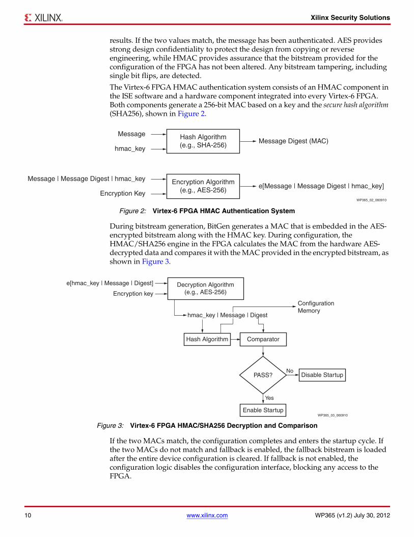
The Virtex-6 FPGA HMAC authentication system consists of an HMAC component in the ISE software and a hardware component integrated into every Virtex-6 FPGA. Both components generate a 256-bit MAC based on a key and the secure hash algorithm (SHA256), shown in Figure 2.
During bitstream generation, BitGen generates a MAC that is embedded in the AES-encrypted bitstream along with the HMAC key. During configuration, the HMAC/SHA256 engine in the FPGA calculates the MAC from the hardware AES-decrypted data and compares it with the MAC provided in the encrypted bitstream, as shown in Figure 3.
If the two MACs match, the configuration completes and enters the startup cycle. If the two MACs do not match and fallback is enabled, the fallback bitstream is loaded after the entire device configuration is cleared. If fallback is not enabled, the configuration logic disables the configuration interface, blocking any access to the FPGA.
X-Ref Target - Figure 2
Figure 2: Virtex-6 FPGA HMAC Authentication System
Hash Algorithm(e.g., SHA-256)
Message Digest (MAC)
WP365_02_060910
e[Message | Message Digest | hmac_key]Encryption Algorithm
(e.g., AES-256)
Message | Message Digest | hmac_key
Encryption Key
Message
hmac_key
X-Ref Target - Figure 3
Figure 3: Virtex-6 FPGA HMAC/SHA256 Decryption and Comparison
ConfigurationMemory
Hash Algorithm Comparator
hmac_key | Message | Digest
Decryption Algorithm(e.g., AES-256)Encryption key
e[hmac_key | Message | Digest]
WP365_03_060910
PASS? Disable StartupNo
Enable Startup
Yes
Xilinx Security Solutions
WP365 (v1.2) July 30, 2012 www.xilinx.com 11
Additional Security FeaturesXilinx FPGAs include additional security features and structures that are used in combination with the security methods described here.
Readback/JTAG DisableAll Xilinx devices with encryption (Virtex-4, Virtex-5, Virtex-6, and Spartan-6 devices) have an SEU-hardened readback disabling circuitry. When encrypted configuration is enabled, triple-redundant logic disables FPGA readback via all external interfaces after the device is loaded with an encrypted design. In addition, this feature blocks reads of the configuration memory via the JTAG interface to hinder reverse engineering efforts.
Readback CRCVirtex-5, Virtex-6, and Spartan-6 devices include a feature that performs continuous readback of configuration data in the background of a user design. This feature is aimed at simplifying the detection of changes in the configuration memory—for example, due to SEUs that can cause a configuration memory bit to flip. This capability can be used in conjunction with the FRAME ECC feature for advanced operations such as SEU corrections. This feature can also be used to detect tampering and side-channel attacks.
System MonitorThe draft standard FIPS 140-3 ([Ref 2] points to the published FIPS 140-2 revision) proposes temperature and voltage monitoring for the highest level of security (Security Level 5) as a means of detecting side-channel attacks.
Virtex-5 and Virtex-6 FPGAs contain a single System Monitor block, built around a 10-bit, 200 ks/s analog-to-digital converter (ADC). When combined with a number of on-chip sensors, the ADC is used to measure FPGA physical operating parameters such as on-chip power supply voltages and die temperatures.
KeyclearThe start-up block in Virtex-5, Virtex-6, and Spartan-6 devices provides users with an internal signal that, when asserted, clears the AES decryption key from the battery-backed RAM. This capability can be part of a response to a tamper event.
IPROGIPROG is an internal command sent through the ICAP interface in Virtex-6 and Spartan-6 devices that clears the FPGA configuration memory, all flip-flop contents, and key expansion memory—but not the key itself. This command effectively clears configuration memory and can be combined with the KEYCLEAR signal in response to tampering.
BSCANThe BSCAN primitive allows user logic to access the JTAG/boundary-scan signals in Virtex-4, Virtex-5, Virtex-6, and Spartan-6 devices. Through instantiations of this block, the designer can construct custom logic to monitor the activity on the JTAG port as a tamper-detection mechanism.
12 www.xilinx.com WP365 (v1.2) July 30, 2012
Conclusion
Device DNATo prevent device cloning, Virtex-6 and Spartan-6 FPGAs contain an embedded, unique device identifier (Device DNA). This unique 57-bit identifier (analogous to a serial number) is nonvolatile and permanently programmed into the FPGA in the FUSE_ID eFUSE register. Because this identifier is programmed into OTP eFUSEs at device final test, it is tamper resistant.
First introduced with the Spartan-3A FPGA, the Device DNA number is used with a customer-defined security algorithm in user logic to generate an active value/checksum. Typically, this value is compared to a pre-stored check value to determine whether design functionality can proceed.
While Device DNA prevents cloning, it does not protect against spoofing per se. However, the custom-designed security function can be constructed to include a dead-man switch output, which can be used elsewhere in the system either to prevent certain other functions from operating or to detect tampering.
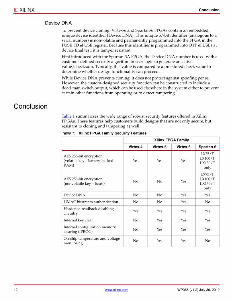
ConclusionTable 1 summarizes the wide range of robust security features offered in Xilinx FPGAs. These features help customers build designs that are not only secure, but resistant to cloning and tampering as well.
Table 1: Xilinx FPGA Family Security Features
Xilinx FPGA Family
Virtex-4 Virtex-5 Virtex-6 Spartan-6
AES 256-bit encryption (volatile key – battery-backed RAM)
Yes Yes Yes
LX75/T, LX100/T, LX150/T
only
AES 256-bit encryption (nonvolatile key – fuses) No No Yes
LX75/T, LX100/T, LX150/T
only
Device DNA No No Yes Yes
HMAC bitstream authentication No No Yes No
Hardened readback-disabling circuitry Yes Yes Yes Yes
Internal key clear No Yes Yes Yes
Internal configuration memory clearing (IPROG) No Yes Yes Yes
On-chip temperature and voltage monitoring No Yes Yes No
References
WP365 (v1.2) July 30, 2012 www.xilinx.com 13
These capabilities can be combined in response to various security needs:
• Confidentiality plus anti-cloning protection: AES• Confidentiality, authentication, plus anti-overbuilding/cloning protection: AES
plus HMAC authentication• Confidentiality, authentication, plus anti-overbuilding/cloning and anti-spoofing
protection: HMAC authentication eFUSE key storage• Confidentiality, anti-overbuilding/cloning protection, plus long shelf life: AES
with eFUSE key storage• Confidentiality and anti-cloning protection for devices without eFuse: Device
DNA
Working with an FPGA vendor who understands today's security threats and has experience in secure design is essential.
References1. M. McLean and J. Moore, FPGA-Based Single Chip Cryptographic Solution, Military
Embedded Systems, 2007.http://www.mil-embedded.com/articles/id/?2069
2. FIPS-140-2, Security Requirements for Cryptographic Modules, Federal Information Processing Standards, U.S. National Institute of Standards and Technology.http://www.nist.gov/itl/upload/fips1402.pdf
3. FIPS-197, Advanced Encryption Standard, Federal Information Processing Standards, U.S. National Institute of Standards and Technology.http://www.nist.gov/itl/upload/fips-197.pdf
4. FIPS-180-3, Secure Hash Signature Standard, Federal Information Processing Standards, U.S. National Institute of Standards and Technology.http://www.nist.gov/itl/upload/fips180-3_final.pdf
5. FIPS-198-1, Keyed-Hash Message Authentication Code, Federal Information Processing Standards, U.S. National Institute of Standards and Technology.http://www.nist.gov/itl/upload/FIPS-198-1_final.pdf
Further Related Information1. S. Trimberger, Trusted Design in FPGAs, Design Automation Conference, June 2007.
http://citeseerx.ist.psu.edu/viewdoc/download?doi=10.1.1.92.6684&rep=rep1&type=pdf
2. Soviet Union Impounds and Copies B-29, National Museum of the USAF. Retrieved: 31 January 2010.http://www.nationalmuseum.af.mil/factsheets/factsheet.asp?id=1852
3. Former Gaming Official Sent to Jail for Slot Scam, Las Vegas Review Journal, 10 January 1998. Retrieved: 31 January 2010. http://www.reviewjournal.com/lvrj_home/1998/Jan-10-Sat-1998/news/6745681.html
4. S. P. Skorobogatov, Low Temperature Data Remanence in Static RAM, Technical Report 536, University of Cambridge Computer Laboratory, June 2002. http://www.cl.cam.ac.uk/techreports/UCAM-CL-TR-536.pdf
5. Managing the Risks of Counterfeiting in the Information Technology Industry, KPMG International, 2005.http://www.agmaglobal.org/press_events/press_docs/Counterfeit_WhitePaper_Final.pdf
6. UG360, Virtex-6 FPGA Configuration, Xilinx user guide.http://www.xilinx.com/support/documentation/user_guides/ug360.pdf
14 www.xilinx.com WP365 (v1.2) July 30, 2012
Revision History
7. WP345, Slash Your Total Cost by up to 50% with Spartan-3 Generation FPGAs, Xilinx white paper.http://www.xilinx.com/support/documentation/white_papers/wp345.pdf
8. UG370, Virtex-6 FPGA System Monitor, Xilinx user guide.http://www.xilinx.com/support/documentation/user_guides/ug370.pdf
9. Saar Drimer, Volatile FPGA Design Security – A Survey, v0.96, April 2008.http://www.cl.cam.ac.uk/~sd410/papers/fpga_security.pdf
10. Saar Drimer, Security for Volatile FPGAs, University of Cambridge Computer Laboratory, November 2009. http://www.cl.cam.ac.uk/techreports/UCAM-CL-TR-763.pdf
11. WP267, Advanced Security Schemes for Spartan-3A/3AN/3A DSP FPGAs, Xilinx white paper.http://www.xilinx.com/support/documentation/white_papers/wp267.pdf
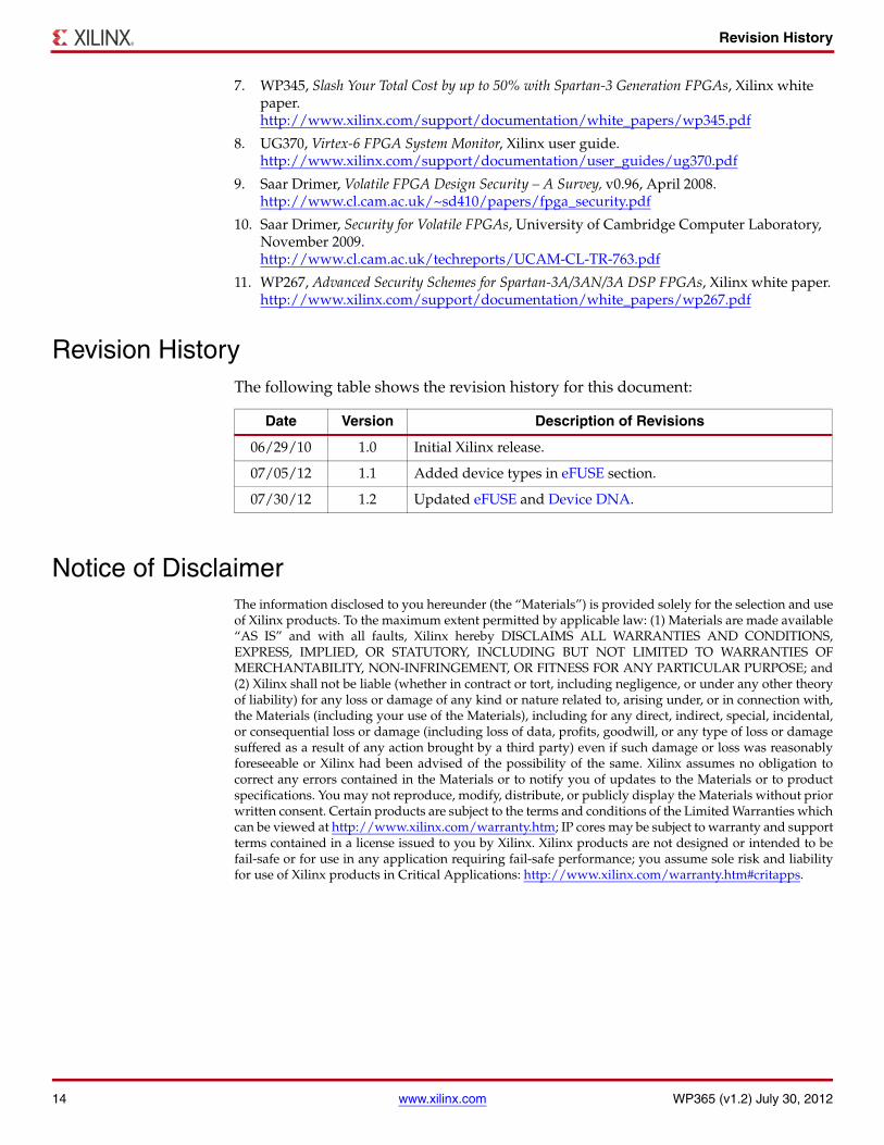
Revision HistoryThe following table shows the revision history for this document:
Notice of DisclaimerThe information disclosed to you hereunder (the “Materials”) is provided solely for the selection and useof Xilinx products. To the maximum extent permitted by applicable law: (1) Materials are made available“AS IS” and with all faults, Xilinx hereby DISCLAIMS ALL WARRANTIES AND CONDITIONS,EXPRESS, IMPLIED, OR STATUTORY, INCLUDING BUT NOT LIMITED TO WARRANTIES OFMERCHANTABILITY, NON-INFRINGEMENT, OR FITNESS FOR ANY PARTICULAR PURPOSE; and(2) Xilinx shall not be liable (whether in contract or tort, including negligence, or under any other theoryof liability) for any loss or damage of any kind or nature related to, arising under, or in connection with,the Materials (including your use of the Materials), including for any direct, indirect, special, incidental,or consequential loss or damage (including loss of data, profits, goodwill, or any type of loss or damagesuffered as a result of any action brought by a third party) even if such damage or loss was reasonablyforeseeable or Xilinx had been advised of the possibility of the same. Xilinx assumes no obligation tocorrect any errors contained in the Materials or to notify you of updates to the Materials or to productspecifications. You may not reproduce, modify, distribute, or publicly display the Materials without priorwritten consent. Certain products are subject to the terms and conditions of the Limited Warranties whichcan be viewed at http://www.xilinx.com/warranty.htm; IP cores may be subject to warranty and supportterms contained in a license issued to you by Xilinx. Xilinx products are not designed or intended to befail-safe or for use in any application requiring fail-safe performance; you assume sole risk and liabilityfor use of Xilinx products in Critical Applications: http://www.xilinx.com/warranty.htm#critapps.
Date Version Description of Revisions
06/29/10 1.0 Initial Xilinx release.
07/05/12 1.1 Added device types in eFUSE section.
07/30/12 1.2 Updated eFUSE and Device DNA.