Embed Size (px)
DESCRIPTION
Sokal - Class E-A New Class of High-efficiency Tuned Single-Ended Switching Power Amplifiers
Citation preview

168
Class E-A NewSingle-Ended
IEEE JOURNAL OF SOLID-STATE CIRCUITS, VOL. SC-10, NO. 3, JUNE 1975
Class of High-Efficiency TunedSwitching Power Amplifiers
NATHAN O. SOKAL, SENIOR MEMBER, IEEE, AND ALAN D. SOKAL
Abstract–The previous literature on tuned power amplifiers has notmade clear the fundamental differences between amplifiers in whichthe output device acts 1) as a current source, or 2) as a switch. Previouscircuits have often operated in contradiction to their design assump-tions, resulting in the need for “cut-and-try” design. The new class of
amplifiers deseribed here is based on a load network synthesized tohWe a transient response which maximizes power efficiency even if the
active device switching times are substantial fractions of the ac cycle.The new class of amplifiers, named “Class E; 1 is defined and is iflus-tnated by a detailed description and a set of design equations for onesimple member of the class. For that circuit the authors measured
96 percent transistor efficiency at 3.9 MHr at 26-W output from a pairof Motorola 2N3735 TO-5 transistors. Advantages of Class E areunusually high efficiency, a priori designability, large reduction insecond-breakdown stress, low sensitivityy to activedevice characteristics,and potential for high-efficiency operation at higher frequencies thanpI eviously published Class-D circuits. Harmonic output and power gain
are comparable to those of conventional amplifiers.
I. INTRODUCTION
1[N a high-efficiency power amplifier, increases of efficiency
which at first might appear to be minor can be very impor-
tant, e.g., increasing collector efficiency from 80 to 90 per-
cent halves the collector power dissipation (reduction from213percentof the input power to 10 percent). That allows
dmtbling the power output, or halving the number of output
t~ansistors and reducing the heat sink volume and weight by a
factor of about 2.8, or halving the junction temperature rise
and thereby decreasing the transistor failure rate.2 The recent
large increases of energy cost provide further incentive for
reducing power losses in high-power fixed installations, and
conservation of battery or generator power can be importantfor portable or remote equipment.
The major power loss is usually power dissipated in the out-
put active device(s), eg., transistors or vacuum tubes. To
minimize that dissipation, one attempts to minimize: 1) the
Manuscript received January 23, 1974; revised January 14, 1975. A
preliminary version of this paper was presented at the 1972 IEEE Inter-national Symposium on Circuit Theory, Los Angeles, Calif., April 1972.
N. O. Sokal is with Design Automation, Inc., Lexington, Mass. 02173.A. D. Sokal is with the Department of Physics, Harvard University,
Cambridge, Mass. 02138.I me new name CCClaSS~ is proposed because 1) the unique Prin-
ciples of load network operation for achieving high efficiency, whichare the basis of our circuit operation, are not embodied in any of the
previously defined Classes A through D and 2) although our amplifierw,es switchhtg active devices, in common with Class D, the definition ofClass D by its inventor [15] does not involve our type of load network,
and specifies operation of the switches at 50 percent duty ratio, whichis not required in our circuit.
‘For example, by a factor of =14 if the temperature rise is halved
from 130°C to 65°C above a 50”C ambient (i.e., T~ is reduced from180”C to 115”C). This factor is an average of values read from graphsfor numerous VHF, UHF, and microwave RF power transistors in “RFand microwave power transistors–MTF projections,” Communications
Transistor Corp., San Carlos, Calif., Bull. 2. O.8.lB, Nov. 1972.
voltage across the device when current flows through it; 2) the
current through the device when voltage exists across it; and
3) the duration of any unavoidable condition in which appre-
ciable current and voltage exist simultaneously. Clas8-C
amplifiers [1] - [8] apply 1) and 2). Class-D amplifiers [2],
[15] -[21] apply 1), 2), and 3). Previous approaches to 3)
have been only to reduce the device switching times. Our new
class of high-efficiency amplifiers is based on a load network
which is synthesized to give a transient response which
achieves 3) even if the device switching times are appreciable
fractions of the ac cycle. For lack of space, we discuss here
only briefly: 1) the largely-ignored fundamental differences
between amplifiers using active devices a) as switches and b) as
current sources, and the greatly different requirements placed
on load network design by those two different cases; 2) the
consequent invalidity of the assumptions upon which many
designs are based; 3). evaluation of previous published work in
tuned power amplifiers; and 4) design of the optimum tran-
sistor for use in this circuit. More details are available on
request from the authors.
II. PREVIOUS WORK
A. Amplifiers Using Current-Source Active Devices
In designing a tuned Class-C power amplifier [1] - [8], the
output active device is assumed to be a high-impedance current
source, i.e., its output current is 1) determined primarily
by the input drive and 2) substantially independent of the
output voltage which results from the flow of that current in
the load network. That network is designed so that its voltage
response to the periodic current pulses is a sinusoid at the
output frequency, with these properties: 1) the minimum of
the voltage across the current source occurs at the time of the
current pulse; and 2) at this minimum, the voltage is not less
than a certain minimum permissible voltage, determined by
the characteristics of the active device and required for the
device to function as a current source as assumed. This voltage
prevents “saturation” of a transistor or “bottoming” of a pen-
tode or triode4 vacuum tube, for example. If the active device
3The work reported here is the subject of patent applications by the
authors. Licenses and further technical information are available tointerested parties.
4 Despitethefact that the triode plate resistance (rp) maY be com-
parable with the tank parallel load resistance (RL), in most cases thetriode acts essentially as a current source unless the tube is “bottomed”
during the current pulse by incorrect circuit operation. Specifically, if
the tank loaded Q is greater than 2rrDRL/rp, where D is the fraction of
a cycle during which the current pulse flows, the current pulse magni-tude will be 80 percent or more of the value it would have if the triodewere a pure current source with infinite rp. For example, for the tYpi-
cal case of D = 0.1 and RL/rp = 4, the triode can be considered to be acurrent source if the tank loaded Q is 2..5 or more, which is almostalways the case.

SOKAL AND SOKAL: NEW CLASS OF POWER AMPLIFIERS 169
TABLE IUSE OF CURRENT SOURCE VERSUS TWO. STATE SWITCH
Characteristic Amplifier Using Current Source Amplifier Using Two-State Switch
Active-device output-port ac imped-
ance (av/az).
Is the active device attowed to
saturate?
Desired voltage across the active
device while conducting current.
What determines the voltage across
the active device while it is conduc-ting current ?
Does the voltage across the activedevice output port during current
conduction depend on the loadnetwork input-port impedance?
What determines the current whichflows through the active device
when it is conducting current?
To what criteria should the loadnetwork be designed?
Always high.
No.
Greater than a specified minimumvrdue.
The voltage response of the loadnetwork input-port impedance to
the current pukes delivered by thecurrent source.
Yes.
Only its input signal.
The input-port voltage wave-form produced in response to aspecified repetitive current-pulsetrain injected into its input port.
“on”: low“off”: high.
Often intentionally, when “on.”
As low as can be obtained.
The voltage approaches zero
because of the low-impedance
property of the “on” switch,independent of the propertiesof the load network.
No.
The load network to which itsoutput port is connected.
The input-port voltage waveformproduced by repetitive alterna-
tively connected short-circuitsand open-circuits at its input port.
(The full use of thk criterion isnovel; detaits are in Section III
of this paper.)
saturates, the basic design assumptions become invalid. This is
the reason why so much “cut and try” is needed in contem-
porary RF power amplifier design.
Harmonic resonators can be added to the load network to
improve the tradeoff between efficiency and conduction angle
[9] -[14]; this provides approximately a flat-bottomed voltage
waveform when the network is driven by the pulsed current
source, extending the duration of the low-voltage condition
and permitting a wider current pulse without severe loss of
efficiency. This circuit, also, requires the minimum voltage
across the current-source device.
All current-source amplifiers dissipate substantial power in
the active device because the voltage across that device during
the current pulse must be larger than the minimum permissible
value, typically of the order of 10 percent of the dc supply
voltage. Obtaining high efficiency requires that the current
pulse amplitude and the load network be adjusted carefully to
obtain an ac output voltage amplitude which is: 1) large
enough to bring the active-device voltage as close to zero as
allowable during the current pulse, but 2) not so large as to
cause the device voltage to become less than the minimum
permissible voltage, thereby causing the device to be no longer
a high-impedance current source and thus to invalidate the
design assumptions.
B. Amplifiers Using Active-Device Switches
Higher efficiency can be achieved by using the active device
as an on/off switch instead of a high-impedance current source;
the increased efficiency results from reducing the voltage
which exists across the device while current is flowing through
it. While a practical active-device current source requires at
least a certain minimum permissible voltage across itself, an
active-device switch may be operated at a much smaller “on”
voltage. Table I shows the fundamental differences between
the use of a current source to drive a load network and the use
of a switch to drive a differently designed load network. These
important distinctions have been missed by many previous
workers in this field; one exception is Rose [28] . Switching-
mode and current-source active devices are sharply distin-
guished from each other by their output-port ac impedances:
in a switching-mode device, the “on” state ac impedance (i.e.,
~V/iY) is low compared to the ac impedances in the surround-
ing circuit; in a current-source device, the ac impedance (exclu-
sive of incidental reactance which are absorbed into the tuned
circuit) is high compared to the surrounding circuit ac imped-
ances, throughout the ac cycle.
Push-pull Class-D current-switching and voltage-switching
circuits [2], [15] - [17] use parallel-tuned or series-tuned reso-
nant circuits, respectively, driven by two on-off switches (e.g.,
transistors). The inputs are so driven that one switch is “on”
while the other is “off,” each switch being “on” for half of
the ac cycle. These amplifiers are efficient, but suffer from
the possibility of both transistors conducting simultaneously
or being off simultaneously during the switching transient,
leading to loss of efficiency at high frequencies and to the
possibility of transistor destruction by second breakdown
[16]. A further limitation on efficiency at high frequency
and a potential cause of second breakdown for the voltage-
switching amplifier is not mentioned by previous authors: the
power dissipated and the simultaneous high voltage and high
current imposed on the transistors in charging the output-to-
ground capacitance plus the Cob of both of the two switching
transistors to almost the full supply voltage (Vcc), twice each
ac cycle, at the operating frequency (f), in a charging time of
a/f. The power dissipation is (2f)(~)(2C0~ + C’OUtpUt)(Vrx -
2 VCE(wt))2; the second-breakdown stress is a current typically

170 IEEE JOURNAL OF SOLID-STATE CIRCUITS, JUNE 1975
rising linearly from zero to 2(2C’0~ + Coutput)( ~CC - 2 ~Cl!7(sat))
~/a while the voltage falls parabolically from (VCC - VcE(Sat))
to vc~(sat) .
Timing problems of a pair of switches are avoided by using a
single switch in a “single-ended” amplifier. References [18] -
[21 ] describe single-ended circuits operated at up to 80 MHz,
using load networks similar to those of current-source tuned
power amplifiers. They do not consider the possibility of
increasing the collector efficiency through unconventional de-
sign of the load network.
Single-ended amplifiers (e.g., [22] - [27] ) typically are de-
signed as current-source amplifiers, but many allow the active
device to saturate during part of the time that it is conducting
current, invalidating the design assumptions. If this happens
(e.g., because excessive input drive is applied), the device may
then accidentally act as an “on” switch during the time that it
is saturated, but there are the undesirable possibilities of:
1) potentially destructive inverted-mode operation, 2) a mode
of oscillation which has not heretofore been described in
detail, or 3) a substantial increase in broad-band noise output.5
Such an amplifier comprises: 1) an active device which is an
“on” switch for part of the “on” time and a current source for
the remainder of the ac cycle, together with 2) a load network
designed on the assumption of a current-source active device.
A load network designed to provide a specific response to a
train of current pulses from a high-impedance current source
cannot be expected, a pi-ion”, to yield optimum performance
when driven by a cyclically-operated switch which provides an
excitation completely different from that for which the net-
work was designed. The widely acknowledged need for “cut-
and-try” in tuned power amplifier design, and the observed
sensitivity of circuit performance to individual variations in
transistor characteristics, give experimental confirmation of
this hypothesis that designing according to invalid assumptions
may not yield optimum performance. The circuit described
below operates as designed; it is not sensitive to variations in
transistor characteristics.
III. DESCRIPTION OF THE NEW CIRCUIT OPERATION
A. General Principles
Fig. 1 is a block diagram of a single-ended switching-mode
amplifier. The active device acts substantially as a switch
when appropriately driven by the driver.G The active device
output is represented as a nonideal single-pole single-throw
switch: the “on” resistance (dc and/or ac) may be nonzero,the “off” resistance (dc and/or ac) may be noninfinite, and
the turn-on and turn-off switching times may be nonzero. As
ACTIVE !
DEVICEINPUT SWITCH
—
DC POWER SUPPLY s~
Fig. 1. Block diagram of single-ended switching-mode amplifier.
the switch is cyclically operated at the desired ac output fre-
quency, dc energy from the power supply is converted to ac
energy at the swit thing frequency (and harmonics thereof).
To obtain maximum fundamental-frequency output, the switch
duty ratio is made approximately 50 percent, i.e., the switch is
“on” for approximately half of the ac period and “off” for the
remainder of the period. The load network may include a low-
pass or bandpass filter to suppress harmonics of the switching
frequency at the load, and may transform the load impedance
and/or accommodate load reactance.
A power amplifier which uses the active device as a switch is
potentially highly efficient because the “on” and “off” states
of the switch fulfill Conditions 1) and 2) of Section I. But in
practical high-efficiency switching-mode amplifiers, even with
proper driver design and choice of switching active device, the
switching time of the device may be a considerable fraction of
the ac cycle, and considerable power may be dissipated in the
active device during switching, in violation of Condition 3).
The novel principle of the tuned power amplifier described
here is to avoid by design the simultaneous imposition of sub-
stantial voltage and substantial current on the switch, even
during switching intervals of substantial duration, through the
use of a load network synthesized to yield an optimal tran-
sient response to the cyclic operation of the switch.
Fig. 2(a) and (b) shows the desired waveforms of voltage
across the switch and current through the switch, in a circuit
of the Fig. 1 class arranged for maximum power efficiency.
The following conditions are met by those waveforms.
1), 2) Conditions 1) and 2) of Section I: Those conditions
are well known, and require only that the active device be
chosen and the driver be designed so as to minimize the
switch “on” voltage and “off” leakage current, respectively.
Those conditions are substantially independent of the design
of the load network.
3) The switching time of the switch is minimized: This con-
dition is also well known, and may also be fulfilled by proper
choice of the active device and proper design of the driver.
This condition is somewhat dependent on the design of the
load network, although previous work has not taken cogni-
zance of this dependence. To the extent that the load network
design does af~ect the switching time, it will be seen below5fie potentially destructive operating conditions and the oscillation
are subjects of planned future papers by the authors. The noise effectthat our load network causes the switching time to be de-
has been observed in unpublished work on oscillators by M. Crandall of creased compared with that attained with prior-art load
Microwave Associates, Inc., and others. The reasons for it, and experi- networks.mentaJ data, are subjects of a planned future paper by the authors.
The mechanism believed to be responsible for this noise increase existsThe load network is arranged to have the input-port tran-
SJSOin volta~e-switchirw Class-D amplifiers, but does not exist in the sient response described in 4) through 8) below..authors’ switching-mode amplifier. 4) Voltaze delay at switch turnoffi In the time interval
6 ‘J’he drive waveform can be optimized on the criteria of efficiency,during whi~h the ‘switch makes its t~ansition from the “on”
power gain, and freedom from transistor second breakdown. The opti-mum drive and resulting power gain for transistor switches and for state to the “off” state, the voltage across the switch remains
vacuum-tube switches are subjects of planned future papers. low for a time long enough that the current through the

SOKAL AND SOKAL: NEW CLASS OF POWER AMPLIFIERS 171
(a)
(b)
Fig. 2. Optimum waveforms in circuit of Fig. 1 arranged for maximum
power efficiency. (a) Voltage across switch. (b) Current throughswitch.
switch has by then been reduced substantially to zero. Then
the voltage increases. This assures that high voltage does not
exist across the switch while the current through it is nonzero,
thereby avoiding the energy loss which would have existed if
the voltage had been allowed to start to increase before the
current decrease to zero had been substantially completed.
5) Voltage return to zero at switch turnon: During the
switch “off” state, the load network input-port transient re-
sponse carries the voltage across the switch first upwards, and
then downwards toward zero; this voltage reaches zero just
prior to the start of the switch “on” state, i.e., just before
current begins to flow in the switch. This avoids the energy
dissipation which would have occurred if the switch current
had begun flowing while the voltage across the switch was still
high, and had thereafter discharged to ground, through the
switch, the capacitance at the load network input port.7
6) Zero voltage slope at switch turnon: When the “off”
state transient response reaches zero voltage across the switch,
i.e., just before the beginning of the “on” state, it does so with
approximately zero slope (i.e., du/dt x O). This permits acci-
dental slight mistuning of the amplifier without severe loss of
efficiency, i.e., there is a time interval during which the
switch turnon can occur while still substantially meeting the
condition of u = O. Moreover, moderately slow turnon of the
switch does not cause the switch to experience high power
dissipation during turnon, because the voltage across the
switch is not increasing rapidly during the time that the switch
is turning on. Furthermore, the conditions v = O and dvldt = O
at the end of the “off” state together imply that the switch
7~is capacitance includes intrinsic switch capacitance and circuit
stray capacitance, as well as any capacitor purposely designed to be part
of the tuned circuit. Note that each time a capacitance C, initiallycharged to a voltage V, is discharged by a switch, an energy CV2/2 will
be dissipated, independent of the switch seriesresistance. This causesapower lossof C@f/2, reducing efficiency.
current at the start of the “on” state will be zero, and that
during the “on” state the switch current need increase from
zero only gradually. In view of the limited di/dt capabilities
of actual active-device switches, this zero starting current is
desirable because it helps to minimize the active device switch
turnon time, and hence further minimize dissipation during
the turnon transient. Avoiding a substantial negative value of
dv/dt at turnon time avoids imposing on the switch a require-
ment to conduct substantial current then in the reverse of the
usual direction.
7), 8) The voltage and current transient response waveforms
each have a jlat top: It can be shown (available from the
authors) that the optimum voltage and current waveforms are
flat topped with short rise and fall times, the peak values being
equal to or less than the maxima which the switch is able to
withstand reliably, for the usual case in which the switch peak
voltage and current capabilities define the allowable limits of
operation.
The waveforms of Fig. 2, while superficially resembling the
approximately square waves of a switching amplifier driving a
resistive load, differ from the latter in one absolutely crucial
respect: the delay of each waveform of Fig. 2 in increasing
from zero until the other waveform has completed decreasing
to zero. This is accomplished oral’ by appropriate design of a
nonresistive load network, and results in a considerable in-
crease in efficiency if the transition time of the switch is an
appreciable fraction of a half-cycle of the ac waveform. Note
that Conditions 4) through 8) above are entirely independertt,
except that Condition 6) presupposes Condition 5), and any or
All of them may be included in an amplifier incorporating
these general principles. The ideal network can be approxi-
mated to any desired degree, using lumped and/or distributed
elements. For example, the simple circuit described below
used lumped elements and does not have flat-topped voitage
and current waveforms [Conditions 7) and 8)]; the effect of

172 IEEE JOURNAL OF SOLID-STATE CIRCUITS, JUNE 1975
Fig. 3. Circuit diagram of simple member of the new class of high-efficiency amplifiers.
the flat-topped waveforms on efficiency is often smaller than
that of the delays.
B. Description of a Simple Member of the New Class of
Amplifiers
The above principles will now be illustrated by a simple
member of this new class of amplifiers, shown in Fig. 3, and
the modifications of it shown in Figs. 5,6, and 7. L 1 is a high-
reactance Vcc shunt-feed choke. The sum of its shunt capaci-
tance, the transistor output capacitance, and wiring capaci-
tance is absorbed into Cl and is hereafter called COUt. At high
enough frequencies, all of Cl may be supplied by COUt.8 R
may be the actual load, or may be the input-port resistance of
a low-pass or bandpass falter inserted between the C2-L2
branch and the load to suppress harmonics of the switching
frequency. Reactance of the load or of the input port of such
a filter is absorbed into L2 and/or C2, as described in Section
III-C below.
In the circuit of Fig. 3, the collector voltage is at VcE(,atj
while the transistor is on, meeting Condition, 1) of Section
III-A above. When the transistor is switched off, the load
network transient response is the response of a damped
second-order system, the series connection of L2, R, and
Cl “ C2/(Cl + C2), starting with a set of given initial energies
stored in Cl, C2, and L2. (L 1 is sufficiently large to act as a
source of substantially constant current.) Some of the energy
stored in Cl, C2, and L2 is delivered to R (the network damp-
ing, but also the, usefui load) during the ringing transient.
Cl insures that in the time interval during which the tran-
sistor is being turned off, VCE remains relatively low until
after the collector current has reduced to zero, approximating
(with a parabolic section) the delay of voltage rise shown in
Fig, 2 and discussed above as Condition 4). High VCE does
not occur until after lC has been cut off at low voltage and the
base has become reverse-biased. Thus the BVCEV rating
applies to the “off” condition, rather than the lower B VCEO
STo the extent that the susceptance of L 1 is not negligibly Small in
the frequency range of interest, Cl may be increased to provide theoperating characteristics which are described here for the case of theL 1 susceptance being negligibly smatl. In some cases it may be
desirable to choose a value for L 1 which yields appreciable susceptance,thereby increasing the required capacitance of Cl, as, for example, ifmore than the value required for Cl with negligibly small L 1 suscep-
tance is already supplied by Cout.
or B VCER ratings as in some conventional amplifiers. This
allows using a higher value of Vcc, thereby obtaining higher
power output and higher efficiency.
Three possible kinds of transient response voltages are shown
in Fig. 4, for three different values of damping corresponding
to three different values of network loaded Q(QL). With too
much damping (QL too low) shown in Fig. 4(a)-(c), the volt-
age across Cl never returns to zero. Therefore the transistor
must discharge Cl from some positive voltage V to a near-zero
voltage when it is next turned on, requiring the power dissipa-
tion described in footnote 7. In addition, the transistor is
subjected to simultaneous substantial collector-emitter voltage
and substantial collector current (the “on” collector current
which flows at that VCE according to the input drive provided
by the driver). This transient condition can cause second
breakdown, potentially destructive to the transistor. Previous
published circuits subjected the transistor to this power-
dissipating and potentially-destructive condition (e.g., [29] ;
see VCE waveform of Fig. 2 there). The circuit described here
is specifically designed to avoid this undesirable condition,
helping to assure reliability.
With too little damping (QL too high), shown in Fig. 4(d),
VCE swings below zero, placing the transistor in the inverted
mode. If this voltage is below the base “off” voltage provided
by the driver, the transistor is placed in the active inverted
mode with the base-collector junction forward-biased and the
base-emitter junction reverse-biased. The load will pull the
base further negative by an amount which depends on the
base signal source impedance and voltage, the load network
transient response, and the transistor inverted-mode gain and
cutoff frequency. Several outcomes are possible: 1) the
BVEBX rating may be exceeded and the transistor may be
damaged; 2) BVECX (never specified) may be exceeded and
the transistor may be damaged; 3) appreciable inverted col-
lector current may flow [observable in Fig. 4(d)] , dissipating
power (hence reducing efficiency) and possibly damaging the
transistor; or. 4) no damage will result. This underswing can
also occur in conventional Class-B and Class-C amplifiers.’
Both in conventional amplifiers and in amplifiers of the new
class described here, damage can be prevented by adding a
commutating diode between the collector and emitter as shown
in Fig. 5(a), or between the base and emitter as shown in Fig.
5(b), or by designing the base drive circuit properly.g
With correct damping (QL correct), shown in Fig. 4(e), the
peak negative-going VCE just reaches VcE(Sat)(~O), avoiding
the two above undesirable conditions. The correct damping
also gives zero slope to th-e VCE waveform as it reaches the
gA useful result of adding the diode at the base rather than at the
collector is that the resulting base current injects charge into the baseregion, preparing the transistor to conduct collector current in thenormal direction when the subsequent “on” state begins. Dependingon the design requirements and constraints of a particular application(including the turn-on drive available from the driver), it maybe advan-tageous to choose QL slightly higher than optimum, to allow the loadcurrent to aid in turning on the transistor. However, use of this possi-bility to an excessive extent can lead to a mode of oscillation which canoccur in conventional amplifiers with or without the base diode, and
which appears not to have been reported previously; that is the subject
of a planned future paper.

SOKAL AND SOKAL: NEW CLASS OF POWER AMPLIFIERS 173
..4 (a)
>,\ ,- (b)
~~fd)
(e)
Fig. 4. VCE (lower trace) and lC (upper trace) for circuit of Fig. 3
operating at 10.5 MHz. Incorrect element values can cause positivevoltage at transistor turnon, with zero-slope condition occurring
(a) too early, (b) at correct time, or (c) too late; or they can cause(d) negative voltage at turnon. Correct element values give (e) zero-
voltage, zero-slope condition at turnon. Vertical: 10 V or 0.5 A/div.;
horizontal: 10 ns/div. Ringing after turnon in (a)-(d) is due to induc-tance of current-measuring instrumentation.
rl’-’---
Fig. 5. Addition of commutating diode to transistor.(b) At base.
(a) At collector.
zero value at the end of the “off” half-cycle. This zero value
and zero slope realize Conditions 5) and 6) of Section III-A
above.
A nearly sinusoidal fundamental-frequency current flows iri
the branch L2-C2-R, (The harmonic content is primarily
second harmonic, of amplitude *0.50/QL relative to the fun-
damental, e.g., s5.0 percent (-26 dB) for QL = 10.) The
collector current waveform is approximately a section of a
sine wave, as shown in Fig. 4(e); D below gives numerical
details. Depending on the transistor storage time and the
technique used to accommodate it, the transistor is operated
in saturation or in the active region just outside of saturation. 10
C. Circuit Element Values
The element values for the circuit of Fig. 3 are obtained by
choosing the three variables Cl, C2, and L2 to meet simul-
taneously the three following mathematical conditions.
1) VCE = O at t= (1 - D)(l /-f) after switch turn-off time,
where f is the operating frequency and D is the switch duty
ratio, here taken as 50 percent.
10If it is in the active region, the transistor is made to have a low out-
put impedance while remaining active (i.e., to act as a switch as defined
here) by use of a Baker clamp [30]. We recommend allowing the tran-sistor to saturate (for higher efficiency) and coping with the storage
time by proper circuit design. Storage time in RF power transistors
appears not to have been discussed in the literature; that is the subjectof a planned future paper.

174 IEEE JOURNAL OF SOLID-STATE CIRCUITS, JUNE 1975
TABLE IIELEMENT VALUES FOR NEW DESIGN AND CONVENTIONAL DESIGN
Circuit Conventional RatioElement New Design Design New/Conventional
L2 1.72 pH 0.0403 /,tH 42.7(X 162 pF 6111 pF 0.033C2 200 PF -l/-R 18.0 ~ 0.0422 Q 42.7
2) dVcE/dt = O at t =(1 - D)(l/f) after switch turn-off made between efficiency and harmonic content of the power
time. delivered to the load. Then
3) QL is any chosen value, which may be chosen as dis-cussed immediately below. A specific C1/C2 ratio [see (4)]
makes that chosen QL provide the proper damping shown in
the “QL correct” curve of Fig. 4(e), yielding the zero-slope
zero-value VC~ at turn-on time.
The choice of QL involves a tradeoff among 1) low harmonic
content of the power delivered to R (high QL), 2) high effi-
ciency (low QL ), and 3) complexity of the filter (if any) used
for addition~ harmonic suppression. An optimal design mini-
mizes the total loss in the load network and the subsequent
filter (if any) while meeting a specified maximum limit for
harmonic output at the load. Equations will now be given for
the element values of the Fig. 3 member of the new class;
equations for the resulting performance are in Section III-D
below. The derivations are too long to give here; they are
available from the authors. 11 The equations here are for 50
percent duty ratio; modified ones hdd for other values of
duty ratio,
The values of R and P’cc are constrained by the requirement
to deliver a specified power output to the load from the Vcc
power supply; specifying either one dictates the other. For
highest efficiency, the highest possible Vcc should be used,
within the VCE limitation of the transistor, as will be seen in
(8) below. The maximum allowable Vcc can be found from
(7). The value ofl? is found as’z
()R = (VCC - VC..@t))2 2 = 0577 (Vcc - v@a*))2
P ?r’ “ P“7+1
(1)
Impedance transformation can be used if the load resistance is
not equal to this value of R; seeE below. The desired QL may
be chosen freely, according to the design compromise to be
11Equations (1)-(8) agree, in the limit case of {QL = -, VCE(sat ,/=0
tf = O}, with the results of an independent theoretical analysis o thatcase by F. H. Raab (unpublished). Equations (3), (5), (7), and (8) useRaab’s derivation of” Cl. The quantities 1.42(+ 0.10), 2.08(* 0.05),
0.82(t 0.10), and 0.50(+ 0.09) in (4)-(8) are derived from experimentalmeasurements by the authors and their colleague, M. Chessman.
lzHere R is the total resistive load presented to the transistor: the
sum of the input resistance of the load (or the filter, if used) and theseries ac resistances of L 2 and C2, plus an’ “equivalent” lumping of theac losses of L 1 and Cl. P is the total power delivered by the transistorto R as just defined. DC losses in L 1 are accounted for by using aneffective value of Vcc which is lower than the dc power supply voltage
by the value of the dc voltage drop in the dc resistance of L 1.
L2 = QLR/2rrf, from the definition of QL. (2)
To satisfy the conditions VCE = O and dVcE/dt = O at t= 0.5/f
after switch turnoff, given the chosen QL,
“=1’2nfR(:+’)(:)= ’’2nfR5447
and
c2=((2~i2L2)t+Q:~08)
( )(5,447— 1+
1.42
z C1 QL .)QL -2.08 “
(3)
(4)
Note that L2 is not resonant at f with C2 or with the series
combination of Cl and C2. Load reactance (if any) is accom-
modated by absorbing it into C2 and L 2: the inductance of
L2 is decreased if the load series reactance is inductive, the
capacitance of C2 is increased if the load reactance is capaci-
tive, or both are done if the load is a combination of induc-
tance and capacitance (e g., a radio transmitting antenna or an
ultrasonic transmitting transducer). 13
Table II shows the circuit element values for amplifiers with
the topology of Fig. 3 as realized with a conventional design
(e.g., [22] or [26]) and with our design; the element values
are seen to be greatly different. This example is for an ampli-
fier to deliver 20 W at 10 MHz, using QL =6, Vcc = 27 V dc,
L 1 = RF choke, and VcE(Sat) = 2V.
D. Performance Equations and Experimental Results
The dc collector current of the transistor Q, while delivering
ac power P, is
13The impedance of an actual load may be more complicated than
the series combination of a frequency-independent R and a frequency-independent L and/or C. Hence the effect of the load reactance maynot be precisely the same as an effective increase in L 2 and/or decrease
in C2. However, for reasonably well-behaved load impedances, the neteffect is only a small change in the voltage and current wave-shapesfrom those which would have existed if the output branch had con-sisted solely of frequency-independent elements C2, L2, and R. This isbecause by far the principal component of the current entering the loadfrom L2-C2 is of frequency I harmonic-frequency components aresmall. Therefore the impedances at ~ are the most influential ones; the
impedances at harmonic frequencies have correspondingly less influenceon the voltage waveforms.

SOKAL AND SOKAL: NEW CLASS OF POWER AMPLIFIERS 175
P[Dc . —
[
1- (2m4)2/12
v~~1- (2m4)2 /6 - 1‘;~(1 +A - (2nA)2/6)
(5)
where A ~ (1 + 0.82/QL ) ftf,and where ~ is the operating
frequency and tfis the collector current fall time (100 to O
percent of a linear ramp) during transistor turnoff. The collec-
tor current waveshape is determined by the load network and
is approximately a section of a sine wave (between -32.5° and
+147.5° in angle) centered at 1 = lBC. Current builds up
gradually from zero at the beginning of the “on” half-cycle to
a peak value of
=I~C [1 + 1.862(1 - 0.50/QL)]. (6)
It then decays gradually to 21DC (1 + 0.82/QL), at which time
the transistor is suddenly turned off by the drive signal applied
to its base-emitter junction. The peak collector-emitter volt-
age is
[ ~ (e+,)’’’-,]Vc~P~ = ,Vcc + 27rarcsm ~
0 [Vcc - VCE(,,t)] = 3.562 VCC -2.562 V&(,,~).
(7)
These peak and dc values must be within the safe operating
region of the transistor. The most stressful condition is turn-
off of X21DC linearly with time while VCE is rising para-
bolically. The collector efficiency is P/ VccI~c, from (5),
1- (2mi)2/6 - ‘;::t) (1 + A - (2m4)2/6)
T’c =1- (27rA)2/12
(8)
The authors measured 26-W output at 3.9 MHz from a paral-
leled pair of Motorola 2N3735 TO-5 transistors in the circuit
of Fig. 3, with only 4 percent of the dc input power dissipated
in the transistors. Inductor power losses were 3.5 percent in
L2 and 0.7 percent in L 1. All observations agreed with the
above equations to within instrument accuracies. Circuit
parameters were: L 1 = 63 turns AWG 24 on Indiana General
CF1l 1-Q2 ferrite toroid (x68 pH + 0.1$2 de), L2 = 3.45 pH +
0.4 !i2 ac, Cl = 713 pF, C2= 600 pF, R = 10.3 fl, and
23.1 V dc.
E. Further Remarks
Impedance Transformation and cob Neutralization:
Vcc =
Fig. 6
shows how additional windings change L 1 to a transformer
T1 which transforms the load impedance. Leakage inductance
between the T1 windings can be absorbed into L2; this in-
creases the efficiency by eliminating the losses of the portion
of L2 replaced by the leakage inductance. Fig. 7(a)-(c) shows
C2 L2
$Fig. 6. Impedance transformation between load and switch by adding
a winding to L 1.
(a)
(b)
CIA
2rrriz!13(c)
Fig. 7. Impedance transformation between load and switch by tapping
a capacitor. (a) and (b) Tapping C2. (c) Tapping Cl.
impedance transformation by effectively tapping Cl or C2; in
some cases C2A can be intinite. Neutralization of transistor
Cob (e.g., to reduce the current which must be supplied to
Cob by the driver) can be accomplished by capacitively cou-
pling the transistor base to an inverting winding on T1.
Tuning: To operate across a frequency band, 1) provision
may be made for varying Cl, C2, and/or L2, 2) fixed element
values can be used with some sacrifice of performance, or
3) more complex load networks can be used. The tradeoff
factors are the same as in conventional amplifiers, but the
design method is different; that is the subject of a planned
future paper. Using a load network slightly more complex
than that of Fig. 3, we achieved single-element tuning across a
1.6:1 frequency band, maintaining the turnon conditions
V = O and dV/dt = O across the entire band.
Optimum Transistor Design: This circuit uses the transistor
in a way quite different from that of conventional RF power
amplifiers. Both RF power transistors and switching transis-
tors (e.g., Motorola 2N3735, National Semiconductor 2N6376,
RCA 2N5262) work well in this circuit, but neither class is
176
optimized in design and construction for this application.
Changes in transistor design and packaging could yield a tran-
sistor which gives even better results in this type of circuit
than what we have obtained so far. Further information is
available from the authors.
Circuit Protection: As with other kinds of high-efficiency
equipment, protection should be provided against accidental
low-efficiency operation (i.e., accidental high power dissipa-
tion) if advantage is being taken of the normal high efficiency
by reducing the heat-dissipation capability. The higher the
operating efficiency, the more important this requirement
becomes.
[1]
[2]
[3]
[4]
[5]
[6]
[7]
[8]
[9]
[10]
[11]
[12]
[13]
[14]
[15]
[16]
[17]
[18]
[19]
[20]
REFERENCES
F. E. Terman, Radio Engineering, 3rd Ed. New York: McGraw-
Hill, 1947, pp. 374-393.M. R. Osborne, “Design of tuned transistor power amplifiers,”
Electron. Eng., pp. 436-443, Aug. 1968.
R. G. Harrison, “A nonlinear theory of Class C transistor amp-
lifiers and frequency multipliers,” IEEE J. Solid-State Circuits,vol. SC-2, pp. 93-102, Sept. 1967.
J. A. G. Slatter, “Au approach to the design of transistor tunedpower amplifiers,” IEEE TYans. Circuit Theory, vol. CT-12, pp.
206-211, June 1965.R. H. Johnston and A. R. Boothroyd, “High-frequency transistorfrequency multipliers and power amplifiers,” IEEE J. Solid-StateCircuits, vol. SC-7, pp. 81-89, Feb. 1972.R. D. Peden, “Charge-driven HF transistor-tuned power ampli-
fier,” IEEE J. Solid-State Circuits, VOL SC-5, pp. 55-63, Apr.
1970.M. A. H. El-Said, “Analysis of tuned junction-transistor circuits
under large sinusoidal voltages in the normal domain–Part 1: The
effective hybrid-n equivalent circuit,” IEEE Trans. CircuitTheory, vol. CT-17, pp. 8-12, Feb. 1970.— “Analysis of tuned junction-transistor circuits under largesinusoidal voltages in the normal domain–Part II: Tuned poweramplifiers and harmonic generators ,” IEEE Trans. Circuit Theory,vol. CT-17, pp. 13-18, Feb. 1970.V. J. Tyler, “A new high efficiency high power amplifier,”Marconi Rev., vol. 21, pp. 96-109, 1958.
N. S. Fuzik, “Biharmonic modes of a tuned RF power amplifier;’Radio Eng., vol. 25, no. 7, pp. 117-124, 1970.
N. S. Fuzik, E. A. Sadykov, and V. I. Serguchev, “Electricaldesign of the oscillatory circuits of the final stage of a radio
transmitter operating in the biharmonic mode~’ Radio Eng.,vol. 25, no. 1, pp. 141-145, 1970.
J. W. Wood, “High efficiency Class C amplifier,” U.S. Patent
3430157, NoV. 10, 1966.D. M. Snider, “A theoretical analysis and experimental confirma-
tion of the optimally loaded and overdriven RF power amplifier,”IEEE Trans. Electron Devices, VOL ED-14, pp. 851-857, Dec.1967.M. Kitazawa, F. Takahashi, M. Nagaoka, T. Arino, and K. Yama-moto, “Highly efficient 500 kW AM radio transmitter,” ToshibaRev., no. 80, pp. 22-27, Apr. 1973.P. J. Baxandall, “Transistor sine-wave LC oscillators, some gen-eral considerations and new development,” Proc. Insr. Elec. Eng.,vol. 106, part B, pp. 748-758, 1959.
W. J. Chudobiak and D. F. Page, “Frequency and power limita-tions of Class-D transistor amplifiers,” IEEE J. Solid-State Cir-cuits, vol. SC-4, pp. 25-37, Feb. 1969.
D. F. Page, W. D. Hindson, and W. J. Chudobiak, “On solid-state
Class-D systems,” Proc. IEEE (Corresp.), vol. 53, pp. 423-424,Apr. 1965.D. R. Lohrmann, “Amplifier has 85% efficiency while providingup to 10 watts power over a wide frequency band,” Electron.Des., vol. 14, pp. 38-43, Mar. 1, 1966.—“High-efficiency transistor cw rf power amplifier,” U.S. Army
Electronics Command, Fort Monmouth, N. J., Res. Devel. Tech.Rep. ECOM-2836, May 1967.
—“Boost Class-D rf amplifier efficiency,” Electron. Des., vol. 16,pp. 96-99, Jan. 4, 1968.
[21]
[22]
[23]
[24]
[25]
[26]
[27]
[28]
[29]
[30]
IEEE JOURNAL OF SOLID-STATE CIRCUITS, JUNE 1975
G. Oliva and D. R. Lohrmann, “High-efficiency vhf power ampli-fier;’ U.S. Army Electronics Command, Fort Monmouth, N. J.,Res. Devel. Tech. Rep. ECOM-3209, Dec. 1969.R. Hejhall, “Systemizing rf power amplifier design,” Motorola
Semiconductor Products, Inc., Phoenix, Ariz., Application NoteAN-282A, June 1972.D. L. Wollesen, “UHF transmission-line power-amplifier designed
with Smith chart techniques,” Motorola Semiconductor Products,Inc., Phoenix, Ariz., Application Note AN-217, Jan. 1967.F. Davis, “Matching network designs with computer solutions,”
Motorola Semiconductor Products, Inc., Phoenix, Ariz., Applica-
tion Note AN-267, Mar. 1968.C. Leuthauser and B. Maximow, “16- and 25-watt broadbandpower amplifiers using RCA-2N59 18, 2N59 19, and TA7706 uhf/microwave power transistors,” RCA Solid State Division, Somer-ville, N. J., Application Note AN-4421, Oct. 1970.
R. Minton, “Semiconductor high-frequency power-amplifier de-sign,” RCA Electronic Components and Devices, Somerville, N. J.,
PubL ST-3230, Aug. 1966.
T. M. Scott, “Tuned power amplifiers,” IEEE Trans. CircuitTheory, vol. CT-11, pp. 385-389, Sept. 1964.B. E. Rose, “Notes on Class-D transistor amplifiers,” IEEE J.Solid-State Circuits (Corresp.), vol. SC-4, pp. 178-179, June
1969.
R. L. Bailey, “Large-signal nonlinear analysis of a high-power
high-frequency junction transistor,” IEEE Trans. Electron De-vices, vol. ED-17, pp. 108-119, Feb. 1970.R. H. Baker, “Boosting transistor switching speed,” Electronics,vol. 30, pp. 190-193, Mar. 1957.
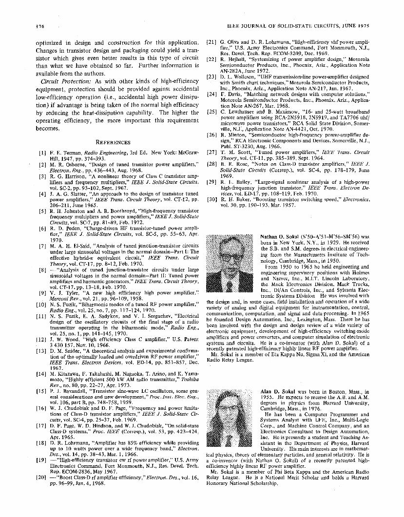
Nathan O. Sokal (S’50-A’51-M’56-SM’56) wasborn in New York, N.Y., in 1929. He receivedthe S.B. and S.M. degrees in electrical engineer-
ing from the Massachusetts Institute of Tech-
nology, Cambridge, Mass., in 1950.
From 1950 to 1965 he held engineering and
engineering supervisory positions with Holmes
and Narver, Inc., M.I.T. Lincoln Laboratory,the Mack Electronics Division, Mack Trucks,Inc.. Di/An Controls, Inc., and Sylvania Elec-tronic Systems Division. He was involved with
the design and, in some cases, field installation and operation of a widevariety of analog and digital equipment for instrumentation, control,
communication, computation, and signal and data processing. In 1965he founded Design Automation, Inc., Lexington, Mass. There he has
been involved with the design and design review of a wide variety ofelectronic equipment, development of high-efficiency switching-mode
amplifiers and power converters, and computer simulation of electronicsystems and circuits. He is a co-inventor (with Alan D. Sokal) of arecently patented high-efficiency highly linear RF power amplifler.
Mr. Sokal is a member of Eta Kappa Nu, Sigma Xi, and the AmericanRadio Relay League.
Alan D. Sokal was born in Boston, Mass., in1955. He expects to receive the A.B. and A.M.degrees in physics from Harvard University,Cambridge, Mass., in 1976.
He has been a Computer Programmer andSystems Analyst with LFE, Inc., Multi-Logic
Corp., and Machine Control Company, and anElectronics Consultant to Design Automation,Inc. He is presently a student and Teaching As-
sistant in the Department of Physics, HarvardUniversity. His main interests are in mathemat-
ical physics, theory of elementary particles, and general relativity. He isa co-inventor (with Nathan O. Sokal) of a recently patented high-efficiency highly linear RF power amplifier.
Mr. Sokal is a member of Phi Beta Kappa and the American RadioRelay League. He is a National Merit Scholar and holds a HarvardHonorary National Scholarship.


![Vibration suppression of cables using tuned inerter dampers · tuned viscous mass dampers [28,29], tuned mass-damper-inerter systems [30] and tuned inerter dampers (TID) [31]. Unlike](https://img.pdfslide.us/doc/110x75/5ebe7d97c8153850be39552a/vibration-suppression-of-cables-using-tuned-inerter-dampers-tuned-viscous-mass-dampers.jpg)