Embed Size (px)
Citation preview
Softbit Detector / Equalizer forGSM release 7
Xia Wu
Kongens Lyngby 2008IMM-MSc-2008-91
Technical University of DenmarkInformatics and Mathematical ModellingBuilding 321, DK-2800 Kongens Lyngby, DenmarkPhone +45 45253351, Fax +45 [email protected]

Abstract
This thesis deals with the implementation of a power/area optimal equalizeraccording to the recently updated GSM specification. The equalizer shouldsupport GMSK, QPSK, 8PSK, 16QAM and 32QAM modulation types. For thehigh order modulation types, the traditional Maximum Likehood Sequence Es-timation(MLSE) algorithm is not able to process the burst within the requiredtime. Therefore two different algorithms with reduced computation complexityare studied in the thesis: the Reduced-State Sequence Estimation with Set-partitioning(RSSE) algorithm and the Sphere Decoding(SD) algorithm. TheRSSE algorithm reduces the complexity by grouping the states into subsets inthe trellis structure, while the SD algorithm addresses the problem by constrain-ing the trellis search with a threshold. Since the two algorithms optimize theMLSE approach in different aspects, a hybrid algorithm (RSSE T) is proposed.The project implemented all three algorithms in RTL and compared their per-formance in area, power and delay. The SD algorithm is implemented in twodifferent approaches, named SD I and SD II. The performance evaluation showsthe area cost of the RSSE, the SD I, the SD II and the RSSE T equalizers is62102 µm2, 94050 µm2, 182965 µm2, and 78317µm2 respectively, for the given45nm CMOS technology. When clocked at 200MHz and given a normal oper-ating voltage between 1.0-1.3V, the power consumption of the four equalizersis typically less than 8.2mW, 6.8mW, 10.3mW and 7.8mW, respectively. TheSD I equalizer is unable to satisfy the timing requirements, thus is the leastinteresting candidate for physical implementation. The RSSE T equalizer con-sumes constantly 30% less power than the SD II equalizer, and in the best casereduces 50% of the power consumed by the RSSE equalizer, therefore it is themost efficient implementation among these four designs.
Keywords: GSM, trellis algorithm, channel equalization, modulation, ASIC

ii

Preface
This thesis was written in partial fulfillment of the requirements for acquiringthe Master of Science degree in engineering. The project has been carried outin 6 months’ duration from 1st March to 30th September, 2008 in Modem IP,Copenhagen, Nokia Denmark. The workload corresponds to 35 ECTS points.The supervisor of the project are Roy Hansen, Nokia Denmark, and AlbertoNannarelli, Informatics and Mathmatical Modelling, Technology University ofDenmark(DTU).
First of all, I would like to thank my supervisors, who have given me invaluablehelp and guidance throughout the project. Also I would like to thank AssociateProfessor Flemming Stassen, who has showed me a lot of support and goodsuggestions during my 2 years’ master study at DTU. A special thank to MortenHansen for several discussion of the subjects related to my thesis work. Also Iwould like to thank the manager of Modem IP, Peter Martensson, and the teamleader, Stig Rasmussen, who gave me the opportunity to work on the project intheir department. Finally, my husband Kehuai and my daughter Sophie, whoare the source of all my inspirations.
Copenhagen, September 2008
Xia Wu

iv

Contents
Abstract i
Preface iii
List of Abbreviation ix
1 Introduction 1
1.1 Project Outline . . . . . . . . . . . . . . . . . . . . . . . . . . . . 2
1.2 Thesis organization . . . . . . . . . . . . . . . . . . . . . . . . . . 3
2 Technology Overview 5
2.1 Modulation Schemes in GSM . . . . . . . . . . . . . . . . . . . . 5
2.2 Pulse shaping . . . . . . . . . . . . . . . . . . . . . . . . . . . . . 8
2.3 GSM frame format . . . . . . . . . . . . . . . . . . . . . . . . . . 8
2.4 Channel model . . . . . . . . . . . . . . . . . . . . . . . . . . . . 9
2.5 Equalizer . . . . . . . . . . . . . . . . . . . . . . . . . . . . . . . 11

vi CONTENTS
2.6 Maximum Likelihood Sequence Estimation (MLSE) . . . . . . . 12
2.7 Reduced-state sequence estimation with set partitioning and de-cision feedback (RSSE) . . . . . . . . . . . . . . . . . . . . . . . . 20
2.8 Sphere detection . . . . . . . . . . . . . . . . . . . . . . . . . . . 23
2.9 Using RSSE in combination with Sphere detection . . . . . . . . 26
3 Design Specification 27
3.1 Requirements . . . . . . . . . . . . . . . . . . . . . . . . . . . . . 27
3.2 Structure Overview . . . . . . . . . . . . . . . . . . . . . . . . . . 36
3.3 OCP interface controller . . . . . . . . . . . . . . . . . . . . . . . 37
3.4 RSSE Equalizer core . . . . . . . . . . . . . . . . . . . . . . . . . 41
3.5 SD Equalizer core . . . . . . . . . . . . . . . . . . . . . . . . . . 57
3.6 RSSE T Equalizer core . . . . . . . . . . . . . . . . . . . . . . . . 73
4 Test and Performance Evaluation 77
4.1 Test Environment . . . . . . . . . . . . . . . . . . . . . . . . . . . 77
4.2 Functional test . . . . . . . . . . . . . . . . . . . . . . . . . . . . 79
4.3 Timing analysis . . . . . . . . . . . . . . . . . . . . . . . . . . . . 79
4.4 Area analysis . . . . . . . . . . . . . . . . . . . . . . . . . . . . . 81
4.5 Power consumption analysis . . . . . . . . . . . . . . . . . . . . . 82
4.6 Energy consumption analysis . . . . . . . . . . . . . . . . . . . . 88
5 Conclusion 93
5.1 Future work . . . . . . . . . . . . . . . . . . . . . . . . . . . . . . 95

CONTENTS vii
A Tail bits definition 97
B Diagrams of the equalizer 99

viii CONTENTS

List of Abbreviation
AWGN Additive White Gaussian NoiseBER Bit Error RateBPSK Binary Phase Shift KeyingDF Decision FeedbackGMSK Gaussian Minimum Shift KeyingGSM Group Special Mobile (Global System for Mobile communication)HT Hilly TerrainI In-phaseISI Intersymbol InterferenceLMMSE Linear Minimum Mean Square ErrorMLSE Maximum Likelihood Sequence EstimationOCP Open Core ProtocolPSK Phase Shift KeyingQ QuadratureQAM Quadrature Amplipude ModulationQPSK Quadrature Phase Shift KeyingRAM Random Access MemoryROM Read Only MemoryRSSE Reduced-State Sequence Estimation with Set-partitioningRTL Register Transfer LevelSD Sphere DecodingSNR Signal-to-Noise RatioTCM Trellis Coded ModulationTU Typical UrbanVA Viterbi AlgorithmVCD Value Change DumpVHDL Very high speed integrated circuit Hardware Description Language

x
Chapter 1
Introduction
Global System for Mobile communications (GSM) has become the current main-stream standard for mobile phones. More future applications have been identi-fied by the mobile phone manufacturers. These applications have increasinglydemanding requirement for cell phone’s energy-efficiency and data processingcapability. The GSM specification has been updated regularly to meet the in-creasing demand of the mobile phone users and manufacturers.
For the release 7 of the GSM specification, it is proposed to add 16QAM,32QAM, and high-rate QPSK to the modulation types that are being usedtoday. These modulation types have larger alphabet size, which consequentiallyincrease data rate. E.g. for 32QAM, the data rate is 5 times as high as thedata rate of GMSK. Unfortunately, the computational complexity of high-ratemodulation types such as 32QAM increases significantly.
It has always been a concern in wireless communication that when transmit-ted through a noisy communication channel, linearly modulated uncoded datais subject to severe Inter-Symbol Interference(ISI). An optimal way for restor-ing signal in detection is to perform Maximum Likelihood Sequence Estima-tion(MLSE) proposed by [2], which estimates the most likely sequence by us-ing Viterbi Algorithm(VA) [3]. The VA is well known for its effectiveness butexponential growth of complexity, thus cannot be directly applied to higher-order modulation types. Considerable amount of research has been carried out

2 Introduction
to find a sub-optimal algorithm which can still reach the BER performanceof the MLSE at reduced computational complexity. One method is to use astructured reduced-state sequence estimator [4]. This method uses Viterbi Al-gorithm(VA) with decision feedback to search a reduced-state “subset trellis”.Another method for performing MLSE in a computational efficient way is theSphere detection(SD) algorithm [5] [6].
Since low area/power cost is a key element in the mobile phone design, it isof great importance to examine and compare the power consumption of thesenear-optimal algorithms. Also, the physical size of the equalizer should be keptas small as possible.
1.1 Project Outline
The main task of the project is to design the equalizer using RSSE algorithm andusing SD algorithm, to optimize both design for area and power, and to comparetheir performance. Furthermore, a hybrid algorithm, called RSSE T, whichcombines the characteristics of the two algorithms is proposed and evaluated.The algorithms used in the project are based on [4], [5], and [6], with somemodifications which make the algorithms feasible for hardware implementation.
To verify the function of the hardware model, a Matlab reference model of theequalizer has also been made. It can both generate test vectors of differentmodulation types, and provide the reference results of the equalizer. The refer-ence model supports the RSSE algorithm, the SD algorithm and the RSSE Talgorithm.
The RTL level hardware models have been made for all three algorithms usingVHDL-93. The functional tests have been carried out in ModelSim. The designhas been synthesized by Synopsys tool suite. The critical path latency and areacost of the gate-level model was checked by using Synopsys Design Compiler(DC). The power consumption of these equalizer models of different algorithmswas measured by PowerTheater 2008 at RTL level. The energy consumptionwas calculated based on the power consumption and the computation time. Thedesign is optimized for area and power at architecture and algorithm level.
The target is 45nm Low Power CMOS technology. In the hardware design,some RAM modules have been used. The RAM modules are simulation modelsprovided by Denali software PureView.
1.2 Thesis organization 3
1.2 Thesis organization
Chapter 1 gives a brief introduction of the project.
In chapter 2, the background knowledge of the project has been presented.These include the modulation schemes and frame format of GSM, frequencyselective channel properties and equalizer, and a short description of the MLSE,the RSSE, the SD and the RSSE T algorithms.
In chapter 3, the design of the equalizer using the RSSE algorithm, the SDalgorithm and the RSSE T algorithm has been described. The major differenceamong these algorithm have been explained in details. A comparison of thecomplexity of design has been made.
The simulation environment has been explained in chapter 4. The functionaltests are described and the simulation results are presented. The area, powerconsumption and energy consumption of the four implementations are measuredand compared.
Chapter 5 describes the future work of further optimization in power and areaand concludes the project.

4 Introduction
Chapter 2
Technology Overview
2.1 Modulation Schemes in GSM
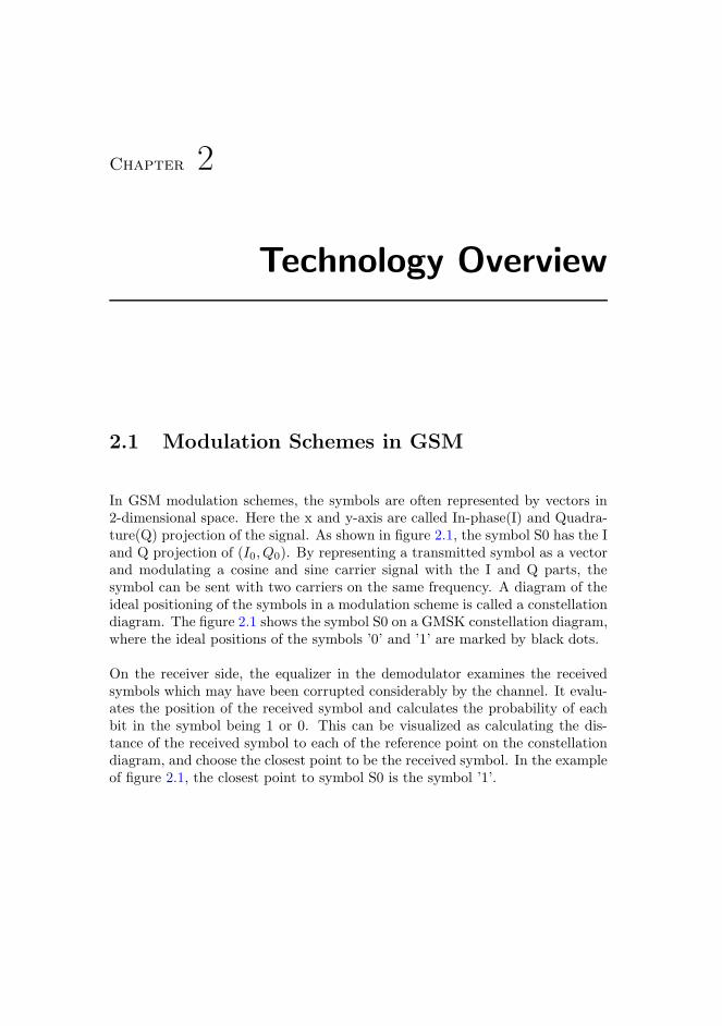
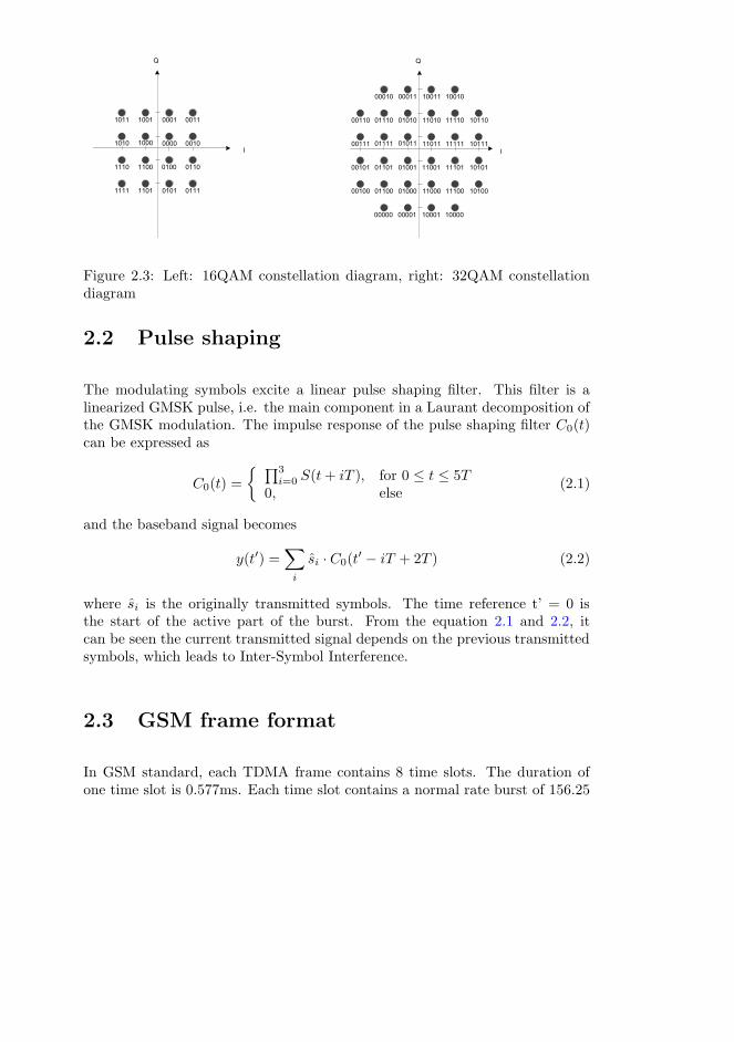
In GSM modulation schemes, the symbols are often represented by vectors in2-dimensional space. Here the x and y-axis are called In-phase(I) and Quadra-ture(Q) projection of the signal. As shown in figure 2.1, the symbol S0 has the Iand Q projection of (I0, Q0). By representing a transmitted symbol as a vectorand modulating a cosine and sine carrier signal with the I and Q parts, thesymbol can be sent with two carriers on the same frequency. A diagram of theideal positioning of the symbols in a modulation scheme is called a constellationdiagram. The figure 2.1 shows the symbol S0 on a GMSK constellation diagram,where the ideal positions of the symbols ’0’ and ’1’ are marked by black dots.
On the receiver side, the equalizer in the demodulator examines the receivedsymbols which may have been corrupted considerably by the channel. It evalu-ates the position of the received symbol and calculates the probability of eachbit in the symbol being 1 or 0. This can be visualized as calculating the dis-tance of the received symbol to each of the reference point on the constellationdiagram, and choose the closest point to be the received symbol. In the exampleof figure 2.1, the closest point to symbol S0 is the symbol ’1’.

6 Technology Overview
2.1.1 GMSK
One of the most commonly used modulation schemes in GSM is Gaussian min-imum shift keying(GMSK). In GMSK constellation diagrams shown in 2.1, thesymbols are (-1,0) and (1,0) marked by black dots, representing symbol ’0’ and’1’. The bits are mapped to symbols according to [7].GMSK has the advantageof having the largest distance between constellation points, and thus the bestimmunity to corruption among the modulation schemes. However, the GMSKcontains only one bit in the symbol and therefore requires more power to trans-mit the same amount of data than other modulation schemes.
��
�
�
��
��
��
Figure 2.1: The In phase and Quadrature projection of a symbol in a GMSKconstellation diagram
2.1.2 PSK
M-ary PSK is a phase shift keying modulation scheme used in GSM. In PSK,the constellation points are usually placed on a unit circle with equal spacesbetween the adjacent symbols, which gives maximum phase-separation. Thesame amplitude ensures the same energy to transmit the symbols.
Each symbol in 8PSK contains three bits. The symbols are Gray mapped intothe constellation diagram, of which the two successive symbols only differ in onebit. In the GSM standard, a modified 8PSK is used, of which the constellationdiagram is rotated by 3/8π. The constellation diagram of 8PSK, defined by [7],is shown in the left side of figure 2.2.
QPSK is one of the more recently supported modulation schemes proposed inGSM release 7. Similar to 8PSK, QPSK is a phase shift keying of four symbols,

2.1 Modulation Schemes in GSM 7
�����������
������������
���������������������
����������
�����������
����������� ����������
�
�
���������
����������
���������
��������
�
Figure 2.2: Left: 8PSK constellation diagram, right: QPSK constellation dia-gram
and each symbol contains two bits. Unlike the GSM and 8PSK modulation,QPSK modulation is only used at high symbol rate of 325k symbol/s, while theformer two operate at a normal symbol rate of 270.8k symbol/s. A 3/4π-rotatedQPSK is proposed by the GSM standard. The constellation diagram of QPSK,defined by [7] is shown in the right side of figure 2.2.
2.1.3 QAM
In the situation of more than eight constellation points, the Quadrature Ampli-tude Modulation(QAM) are used instead of Phase Shift Keying. In the GSMstandard, the constellation points in QAM are arranged in a rectangular latticewith odd-integer coordinated(±1,±3, · · · ). Compared to PSK, the constellationpoints in QAM are distributed more evenly on the constellation plane, whichgive less probability of error. But the inter-symbol difference in both amplitudeand phase makes the modulation more complicated. QAM usually containsmore than 4 bits in one symbol, thus it is used in application which requiredhigh transmission rate.
The GSM release 7 proposed 16QAM and 32QAM, at both the normal sym-bol rate and the higher symbol rate. The constellation diagram of these twomodulation schemes, according to [7], are shown in figure 2.3,
8 Technology Overview
����
�
�
����
����
����
���� ����
���� ����
����
��������
����
����
��������
����
�
�����
�����
�����
�����
����� �����
����� �����
�����
����������
�����
�����
����������
�����
����� ���������������
����� ���������������
�����
�����
�����
�����
�����
�����
�����
�����
�
Figure 2.3: Left: 16QAM constellation diagram, right: 32QAM constellationdiagram
2.2 Pulse shaping
The modulating symbols excite a linear pulse shaping filter. This filter is alinearized GMSK pulse, i.e. the main component in a Laurant decomposition ofthe GMSK modulation. The impulse response of the pulse shaping filter C0(t)can be expressed as
C0(t) =
{ ∏3i=0 S(t+ iT ), for 0 ≤ t ≤ 5T
0, else(2.1)
and the baseband signal becomes
y(t′) =∑
i
si · C0(t′ − iT + 2T ) (2.2)
where si is the originally transmitted symbols. The time reference t’ = 0 isthe start of the active part of the burst. From the equation 2.1 and 2.2, itcan be seen the current transmitted signal depends on the previous transmittedsymbols, which leads to Inter-Symbol Interference.
2.3 GSM frame format
In GSM standard, each TDMA frame contains 8 time slots. The duration ofone time slot is 0.577ms. Each time slot contains a normal rate burst of 156.25
2.4 Channel model 9
� ����� � �
��� ����������
��
�������������� �
����
����
��� ����������
��
��� ���!"��#��������� �"!�������"���$"���"� �!��� �"!�����������%����� �&
��� ����������
�'
�������������� �
����
����
��� ����������
�'
("� �!������%(&
)���� �����)"*����������� �"!�
+�� )�"��,���"�������%+&
%-����!�����.���-�����������"�&
��/01�$�� ��#����� ���!"���%������ �&
���� ���!"��#��������� �"!�������"���$"��)��)��� �"!�����������
�� ����������
�'
�������������� �
����
����
��� ����������
�'
�("� �!�����������)��)��)����� �"!�����
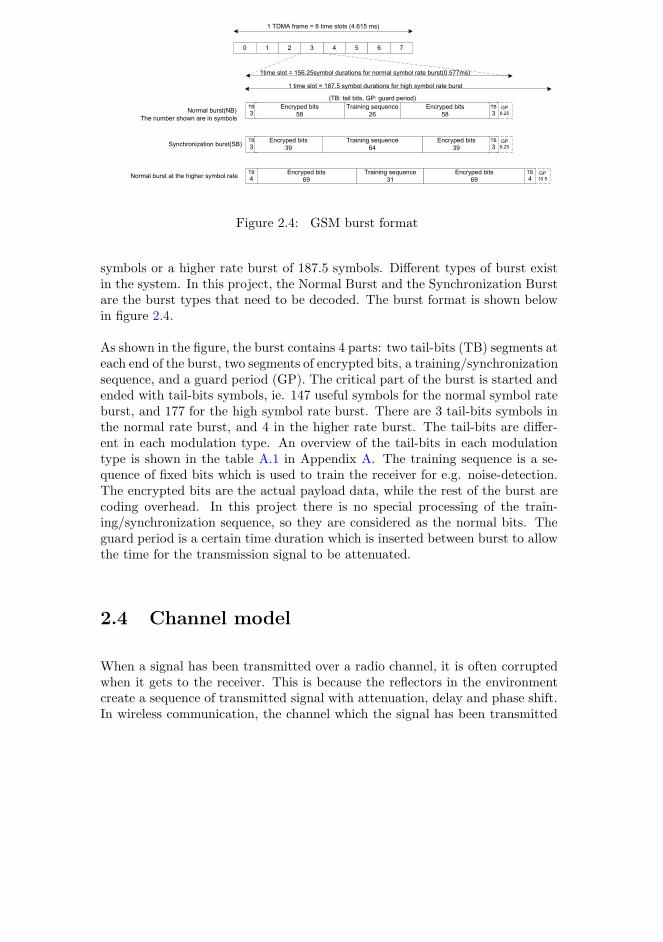
Figure 2.4: GSM burst format
symbols or a higher rate burst of 187.5 symbols. Different types of burst existin the system. In this project, the Normal Burst and the Synchronization Burstare the burst types that need to be decoded. The burst format is shown belowin figure 2.4.
As shown in the figure, the burst contains 4 parts: two tail-bits (TB) segments ateach end of the burst, two segments of encrypted bits, a training/synchronizationsequence, and a guard period (GP). The critical part of the burst is started andended with tail-bits symbols, ie. 147 useful symbols for the normal symbol rateburst, and 177 for the high symbol rate burst. There are 3 tail-bits symbols inthe normal rate burst, and 4 in the higher rate burst. The tail-bits are differ-ent in each modulation type. An overview of the tail-bits in each modulationtype is shown in the table A.1 in Appendix A. The training sequence is a se-quence of fixed bits which is used to train the receiver for e.g. noise-detection.The encrypted bits are the actual payload data, while the rest of the burst arecoding overhead. In this project there is no special processing of the train-ing/synchronization sequence, so they are considered as the normal bits. Theguard period is a certain time duration which is inserted between burst to allowthe time for the transmission signal to be attenuated.
2.4 Channel model
When a signal has been transmitted over a radio channel, it is often corruptedwhen it gets to the receiver. This is because the reflectors in the environmentcreate a sequence of transmitted signal with attenuation, delay and phase shift.In wireless communication, the channel which the signal has been transmitted

10 Technology Overview
over is often referred to as fading multipath channel. The noise presented in thechannel is often assumed as Additive White Gaussian Noise(AWGN). Such achannel can be modeled as a tapped delay line with weight coefficients h which
h = [h0, h1, ..., hL−1] (2.3)
and added with a noise term z, as shown in figure 2.5. The h, also called channelimpulse response, has finite length L. The length L is also known as the lengthof the channel memory. h0 is often assumed to be unity, but in this project tobe scaled to ensure the integer calculation.
�������
�
�����
� �
�
��
� ��
� ����
���
Figure 2.5: The model of a fading multipath channel
When a sequence of symbol sn is transmitted over the multipath channel shownas above, the received signal will be the inner product of the channel impulseresponse with the L most recent transmitted signal, added with a noise term.A discrete-time model of the received symbols can be expressed as
rn =L−1∑
n=0
hi · sn−i + zn, where n = 1, 2, .., NBL + L− 1 (2.4)
where rn is the received symbols, sn is the transmitted symbols, NBL is the burstlength, hn is the channel impulse response and zn is the complex Gaussian noisewith zero mean and variance σ2.
The GSM standard already specified several channel models, such as TypicalUrban(TUx) and Hilly Terrain(HTx). The channel impulse response used inthis project is HT0.
2.5 Equalizer 11
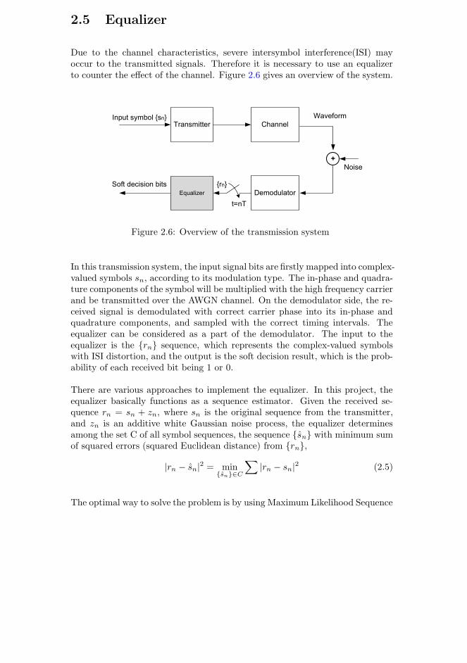
2.5 Equalizer
Due to the channel characteristics, severe intersymbol interference(ISI) mayoccur to the transmitted signals. Therefore it is necessary to use an equalizerto counter the effect of the channel. Figure 2.6 gives an overview of the system.
�������������� ������ ����
������������
���� ������� ����
� ������
����������
�
����
����
!����
Figure 2.6: Overview of the transmission system
In this transmission system, the input signal bits are firstly mapped into complex-valued symbols sn, according to its modulation type. The in-phase and quadra-ture components of the symbol will be multiplied with the high frequency carrierand be transmitted over the AWGN channel. On the demodulator side, the re-ceived signal is demodulated with correct carrier phase into its in-phase andquadrature components, and sampled with the correct timing intervals. Theequalizer can be considered as a part of the demodulator. The input to theequalizer is the {rn} sequence, which represents the complex-valued symbolswith ISI distortion, and the output is the soft decision result, which is the prob-ability of each received bit being 1 or 0.
There are various approaches to implement the equalizer. In this project, theequalizer basically functions as a sequence estimator. Given the received se-quence rn = sn + zn, where sn is the original sequence from the transmitter,and zn is an additive white Gaussian noise process, the equalizer determinesamong the set C of all symbol sequences, the sequence {sn} with minimum sumof squared errors (squared Euclidean distance) from {rn},
|rn − sn|2 = min{sn}∈C
∑|rn − sn|2 (2.5)
The optimal way to solve the problem is by using Maximum Likelihood Sequence
12 Technology Overview
Estimation (MLSE) implemented with the Viterbi Algorithm (VA), which willbe introduced in section 2.6. The computation complexity of this method in-creases exponentially with the size of the symbol in the modulation type. Manyresearches have been undertaken to find an algorithm with reduced complexityand without losing too much BER performance. In this thesis, three differ-ent algorithms have been implemented. These algorithms will be introduced insection 2.7, 2.8 and 2.9.
2.6 Maximum Likelihood Sequence Estimation
(MLSE)
2.6.1 Euclidean Distance and Hamming Distance
A straight line between every two constellation points is called a Euclideandistance. It is same as the concept of distance we use in our daily life. An-other distance term which appears often in the communication is the hammingdistance. Hamming distance stands for the distance between binary sequence.Taking two binary sequence: 011000 and 100001. The distance between thesetwo sequence is the number of bits these two sequence differ, which is 4 in thisexample. A zero hamming distance means the two sequence are the same, whichhas the same interpretation for the zero Euclidean distance.
When discussing the distance between sequences in the following sections, Eu-clidean distance are meant.
2.6.2 Trellis diagram
Trellis diagram is a method to present the state diagram with emphasis onthe time progress of the state transition. Figure 2.7 is an example of a trellisdiagram of a GMSK transmission.
In the trellis diagram, the time is expressed as the horizontal axis on the diagram.The four states S0-S3 in the left-most column are the states at time t=0. Thestates S0-S3 in the second left-most column are the states at t=1, etc. Thestates shown in the figure 2.7 are from t=0 to t=4, progressing from the leftside to the right side. The states which have the same value on the x-axis belongto the same stage.

2.6 Maximum Likelihood Sequence Estimation (MLSE) 13
��
��
��
��
��
��
��
��
�
�
�
�
�
�
��
��
��
��
�
�
�
�
�
�
��
��
��
��
�
�
�
�
�
�
��
��
��
��
�
�
�
�
�
�
�����
�����
�����
�����
�����
�����
�����
�����
�
�
�
�
�
�
�
�
� � � � �
Figure 2.7: Trellis diagram of GMSK
There are four states in each stage, which are marked as S0(0,0), S1(0,1), S2(1,0),S3(1,1). The two number in the bracket indicates the two most recent trans-mitted symbols, with the left item being the oldest and the right item being thenewest. The states representation in this GMSK modulation type example canbe generalized as
State rep : (symb1, symb2, ..., symbN) (2.6)
and symbi = (bi1, bi2, ..., biM ) (2.7)
where symbi is the ith symbol in the represented by the states, N is the numberof symbols in the state memory, bij is the jth bit in the ith symbol and M isthe total bits in one symbol. In this way, a total of 2N states are present ineach stage in the trellis diagram. For example, for an 8PSK 64 state trellis, thememory length N is 2, the bits per symbol M is 3. If one of the states represents(“001”,“100”), it means that two previous transmitted symbols of this state aresymbol “001” followed by symbol “100”.
Each state has 2M possible edges from the previous stage, and 2M possibleedges to the next stage, where M is the bits per symbol. These edges are calledbranches or transitions in the trellis diagram. Each branch is labeled with thecorresponding transmitted symbol. For the trellis diagram in this project, thetransmitted symbols from the same stage are always arranged in their numericalorder, e.g. in GMSK, the uppermost branch for symbol 0, the bottom branchfor symbol 1.
Trellis diagrams are originally used in the binary convolutional codes to visualizethe process of encoding and decoding. Here the trellis diagrams are modifiedsuch that the branch are labeled with modulation symbols instead of binarycode symbols.

14 Technology Overview
Path metric
With the time progresses, the branches are extended into path. The branchesmarked by red line in the figure 2.7 is a path. This path has the initial state ofS0 and the symbol sequence of [1,0,0,1].
Each time the state forks into branches, the weight of each branch is calculated.The weight is the squared Euclidean distance of the received symbol to theexpected symbol. The weight is also called a branch metric. The cumulativedistance(sum of squared error) along a path is called a path metric. In figure2.8 shows an example of the path metric. In this example, the initial state isassumed to be S0, the distance of the received symbol to symbol 0 is calculatedto be 20, and the distance to symbol 1 is 2. Then, at stage t=1, four branchesare calculated. And at stage t=2 and t=3, all eight branches are calculated forbranch metric. This process is called path extension.
��
��
��
��
��
��
��
��
��
�
��
��
��
��
�
��
��
��
��
��
��
�
��
��
�
��
�
��
��
��
��
��
�
�
��
�
��
����
����
����
����
����
����
����
����
�
��
�
�
��
�� �� �� �� �
��
�
��
��
�
��
�
��
��
��
��
�
��
�
Figure 2.8: Trellis diagram of GMSK, with path extension and path merge
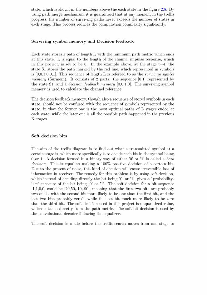
Path merge
In the example in figure 2.8, the eight branches from stage t=2 meets in pairs atstage t=3. When two or more paths meet at the same state, it is only necessaryto keep track of the one with the smallest path metric, because this “winning”path will always have smaller path metric in the following stages. The pathswith bigger path metric are rejected, which are shown as dashed lines in thefigure 2.8. This process is called path merge. The remaining transition from thepath merge process is called a surviving path. Only one path with the minimumpath metric survives among all the possible paths that end at the same state,and the path metric of this surviving path is called the state metric of this
2.6 Maximum Likelihood Sequence Estimation (MLSE) 15
state, which is shown in the numbers above the each state in the figure 2.8. Byusing path merge mechanism, it is guaranteed that at any moment in the trellisprogress, the number of surviving paths never exceeds the number of states ineach stage. This process reduces the computation complexity significantly.
Surviving symbol memory and Decision feedback
Each state stores a path of length L with the minimum path metric which endsat this state. L is equal to the length of the channel impulse response, whichin this project, is set to be 6. In the example above, at the stage t=4, thestate S1 stores the path marked by the red line, which represented in symbolsis [0,0,1,0,0,1]. This sequence of length L is refereed to as the surviving symbolmemory (Surmem). It consists of 2 parts: the sequence [0,1] represented bythe state S1, and a decision feedback memory [0,0,1,0]. The surviving symbolmemory is used to calculate the channel reference.
The decision feedback memory, though also a sequence of stored symbols in eachstate, should not be confused with the sequence of symbols represented by thestate, in that the former one is the most optimal paths of L stages ended ateach state, while the later one is all the possible path happened in the previousN stages.
Soft decision bits
The aim of the trellis diagram is to find out what a transmitted symbol at acertain stage is, which more specifically is to decide each bit in the symbol being0 or 1. A decision formed in a binary way of either ’0’ or ’1’ is called a harddecision. This is equal to making a 100% positive decision of a certain bit.Due to the present of noise, this kind of decision will cause irreversible loss ofinformation in receiver. The remedy for this problem is by using soft decision,which instead of deciding directly the bit being ’0’ or ’1’, gives a ”probability-like” measure of the bit being ’0’ or ’1’. The soft decision for a bit sequence[1,1,0,0] could be [20,50,-10,-90], meaning that the first two bits are probablytwo one’s, with the second bit more likely to be one than the first bit, and thelast two bits probably zero’s, while the last bit much more likely to be zerothan the third bit. The soft decision used in this project is unquantized value,which is taken directly from the path metric. The soft-bit decision is used bythe convolutional decoder following the equalizer.
The soft decision is made before the trellis search moves from one stage to

16 Technology Overview
another stage. A temporary soft decision is calculated at each state, and theminimum soft decision value for each bit is chosen after all the state are calcu-lated. The soft decision is made for the oldest symbol represented by the state,which is the transmitted symbol from the N th-previous stage. And temporarysoft decision is calculated by adding the state metric with the minimum branchmetric to the next stage.
Taking the same example from figure 2.8, at stage t=3 state S0, the soft decisionis made for oldest symbol represented by the state, which is symbol ’0’. Thetemporary soft decision is the state metric of state S0 of 3, added with thecurrent transition of the minimum error, which is 2, and the result is 5. So forthe first state S0, the temporary soft decision made for symbol ’0’ is 5. Similarly,at state S1, the temporary soft decision for symbol ’0’ is 45. At state S2, thesoft decision made for symbol ’1’ is 68. At state S3, the soft decision madefor symbol ’1’ is 89. Then, the smallest temporary soft decision for each bit ischosen, which is 5 for symbol ’0’ and 68 or symbol ’1’. Finally the result ofthe soft decision for symbol ’0’ minus the soft decision for symbol ’1’ is stored,which is -63 in this case. This number can be understood as: the transmittedsymbol from the second previous stage (t=1) is more likely to be 0, with theconfidence of the decision being -63. The more the number is to the negativeside, the larger the probability the symbol being 0 is, and vice versa.
When a state in the trellis diagram represents N recent transmitted symbols,the soft decision at stage T can be made for the symbol at the previous (T-N) stage. The bigger the N is, the more stages the decisions-making stage areaparted from the calculated symbol’s stage, and thus the more precise the resultis, because it allows the error to be cumulated during the past N stage. However,the increase in N will cause the number of total states to grow exponentially.
Summary
By using trellis diagram, the problem of finding the sequence with the min-imum error has become of finding the path with the minimum path metric.The recorded path has the finite length which is equal to the channel memorylength. And the soft decision for a previous transmitted symbol is made at eachstage. The trellis structure shown here is a full trellis structure, which coversall the possible situations of a sequence. This kind of trellis structure is alsocalled a Maximum Likelihood Sequence Estimation(MLSE) trellis. A detaileddescription of how to calculate the path metric, merge the path and find thesoft decision will be described below in the section 2.6.3.

2.6 Maximum Likelihood Sequence Estimation (MLSE) 17
2.6.3 The MLSE algorithm
The algorithm using the full trellis structure is described in this section. Mostcalculations in this section can also be applied to the algorithms described inthe following sections 2.7, 2.8, and 2.9.
It has been described in the section 2.6.2 that each state has a surviving symbolmemory Surmem which contains the best path of length L, with L equal tothe channel impulse response length. Assume that there are Q points in theconstellation diagram and each state represents r previous transitions, therewill be a total of P states in the trellis which P = Qr. The surviving symbolmemory for all the P states at stage x can be expressed as
Surmemx =
symb11 symb12 · · · symb1Lsymb21 symb22 · · · symb2L· · ·
symbP1 symbP2 · · · symbPL
(2.8)
Where each row is a surviving symbol sequence for a state. Taking the survivingsymbol memory of state n (the nth row in the Surmem), and rewriting thesymbol with their IQ coordinates, the estimated sequence of state n becomes:
S(n) = [sn1, sn2, · · · , snL] (2.9)
where sni is the complex representation of symbni. As described in equation2.3, the channel impulse response is h = [h0, h1, · · · , hL−1]. Assume the currentreceived symbol is rx, which is a also complex number indicating the IQ co-ordinates of the received symbol. To counter the channel ISI effect, the innerproduct of the channel impulse response and the estimated sequence is calcu-lated, and is subtracted from the received signal. The result is called a decisionvariable of the current state.
dec var(n) = rx −L−1∑
i=0
hi · sn(L−i) (2.10)
Then the distance (squared error) of the decision variable to each point on theconstellation diagram is calculated. Since there are a total of Q points, and thelist of the IQ coordinates of all these Q points are
Ref = [ref1, ref2, · · · , refQ] (2.11)
where refi is the vector indicating the location of the constellation point on thecomplex plane. The error to each point can then be calculated as
Error(n) = [errn1, errn2, · · · , errnQ] (2.12)

18 Technology Overview
where errnj = dec var(n) −Ref(j); j ∈ (1, Q) (2.13)
Then, the cumulative metric is calculated by adding each error with the statemetric of the current state state met(n),
Cumu met(n) = [cmn1, cmn1, · · · , cmnQ] (2.14)
where cmnj = errnj + state met(n); j ∈ (1, Q) (2.15)
Since there are Q possible new transitions at each state, a number of Q cu-mulative metrics are calculated. A P*Q matrix of cumulative metrics will beobtained for P states, with each row representing one state, and each columnrepresenting a transition to a certain reference point:
Cumu met =
cm11 cm12 · · · cm1Q
cm21 cm22 · · · cm2Q
· · ·cmP1 cmP2 · · · cmPQ
(2.16)
Now the metrics that end at the same state should be merged. As alreadydiscussed in section 2.6.2, for each state, there are Q transitions to the next stage,and Q transitions from the previous stage. For the convenience of explanation,the Cumu met matrix is first transposed into 1D array column by column:
Cumu met 1d = [cm′1, cm′2, · · · , cm′P∗Q]
= [cm11, cm21, · · · , cmP1, cm12, · · · , cmP2, · · · , cmPQ] (2.17)
Then the paths that need to be merged for state n’ in the stage x+1 can bewritten as:
Merging met(n′) = [cm′n′∗Q+1, cm′n′∗Q+2, · · · , cm′n′∗Q+Q] (2.18)
And the surviving metric can be found by selecting the minimum value in theMerging met array. It should be noted that the state metric of the state n’ instage x+1 is the same as the surviving metric of the state n’.
Surviving met(n′) = state met(n′) = mini∈(1,Q)
cm′n′∗Q+i (2.19)
And if there exists I for which
cmn′∗Q+I = mini∈(1,Q)
cmn′∗Q+i (2.20)

2.6 Maximum Likelihood Sequence Estimation (MLSE) 19
The surviving transition trn′ is assigned the value of I. The surviving transitionfor all P state in the state x+1 is
Surviving trans = [tr1, tr2, · · · , trP ] (2.21)
Combining with the matrix in 2.8, the new surviving symbol memory can beobtained for each state in the stage:
Surmemx+1 =
tr1 symb11 symb12 · · · symb1(L−1)
tr2 symb21 symb22 · · · symb2(L−1)
· · ·trP symbP1 symbP2 · · · symbP (L−1)
(2.22)
The initial value of the Surmem can be chosen randomly, as long as the valuematches the state representation. The initial value of the state metric shouldbe set in a way that the initial state has the state metric of zero, and all theother states have the state metric of a maximum value.
Finally, the soft decision should be calculated. Taking the minimum cumulativemetric of each state (row) of Cumu met from equation 2.16,
m cmn = minCumu met(n) = mini∈(1,Q)
cmni (2.23)
For all P state, the minimum cumulative metric is
M cm = [m cm1,m cm2, · · · ,m cmP ] (2.24)
The soft decision is made for each bit in the symbol. Supposing a total of Bbits in each symbol, and 2B = Q. The minimum cumulative metric is firstlyextended to B rows:
M cm 2d =
m cm11 m cm12 · · · m cm1P
m cm21 m cm22 · · · m cm2P
· · ·m cmB1 m cmB2 · · · m cmBP
(2.25)
where each row in the matrix is same as M cm. The soft decision is made forthe previous rth transition, which is stored in the symbnr of state n. If the bth
bit in symbnr is 0, we define m cmbn ∈ g0, otherwise m cmbn ∈ g1. The softdecision for the bth bit in the symbol can be expressed as:
SoftDecb = min (m cmbi ∈ g0)−min (m cmbj ∈ g1) (2.26)
The soft decision is made for all the bits in the symbol.
20 Technology Overview
2.7 Reduced-state sequence estimation with setpartitioning and decision feedback (RSSE)
2.7.1 Set-partitioning
Set-partitioning is proposed by Gottfried Ungerboeck in his publications [9] and[10]. The general idea of the set partitioning is to group constellation points intosubsets, so that the Euclidean distance among the points in the same subset ismaximal.
When the constellation points are set partitioned, the points in a same subsetare the points that are most unlikely to be mistaken with each other. Sincethe most errors are made by picking the neighboring points, rather than thefar-away points, it will be easier to make a decision among the points that arefar-away from each other first. It will be described in the following section thatwhen combining with the trellis diagram, the set partitioning helps to reducethe computation complexity.
As described in his publications, Ungerboeck applied the set-partitioning on theTrellis coded modulation(TCM), which is a combination of convolutional codingscheme and modulation, to achieve an improved coding gain. It should be notedthat in this project, although the set partitioning concept has also been appliedtogether with the trellis diagram, the algorithm has no relation with TCM.
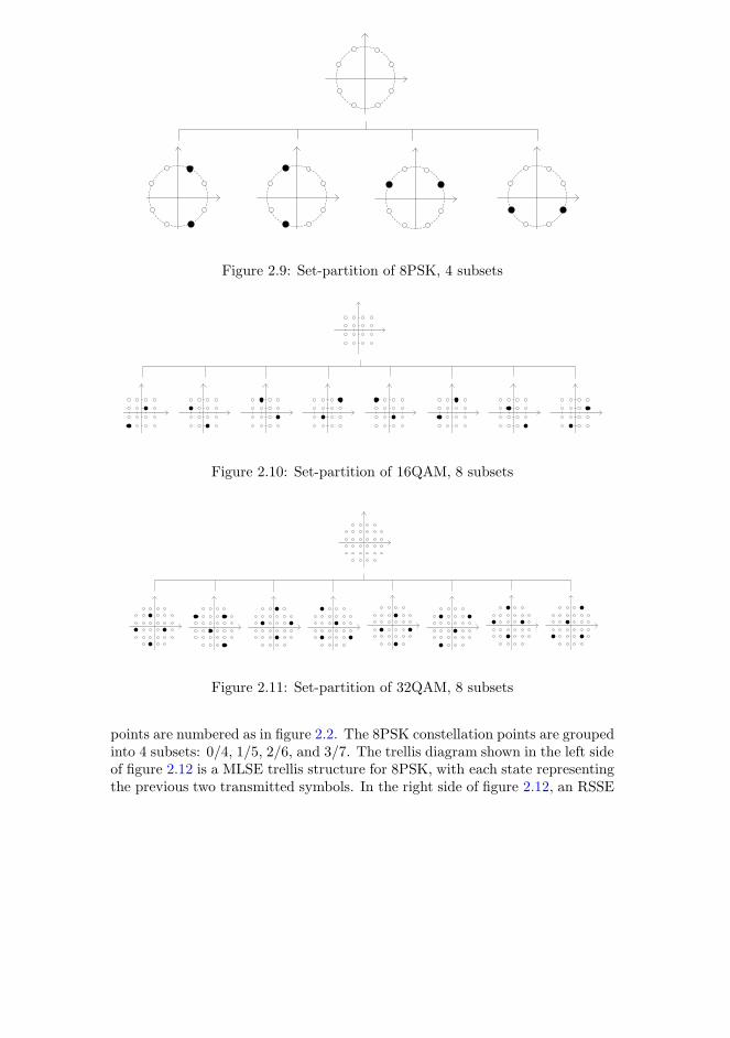
Below are the figures 2.9, 2.10, 2.11 showing how the set partitioning are appliedin the 8PSK, 16QAM, and 32QAM modulation schemes. In this project, theconstellation points are partitioned into 4, 8 and 8 subsets for the 8PSK, 16QAMand 32QAM respectively. It is possible to make further partitioning in 32QAM.
2.7.2 The RSSE algorithm
The algorithm of reduced-state sequence estimation with set partitioning anddecision feedback is proposed by Eyuboglu et.al. in [4]. This algorithm ap-plied set-partitioning on the trellis diagram to achieve reduced complexity incomputation.
The basic concept in this algorithm is that in the trellis structure, when usingthe state to represent the previous transmitted symbols, the state represents thesequence of the subsets instead of the sequence of the symbols. Taking 8PSK asan example. The 8PSK is set-partitioned as in figure 2.9, and the constellation
2.7 Reduced-state sequence estimation with set partitioning and decisionfeedback (RSSE) 21
Figure 2.9: Set-partition of 8PSK, 4 subsets
Figure 2.10: Set-partition of 16QAM, 8 subsets
Figure 2.11: Set-partition of 32QAM, 8 subsets
points are numbered as in figure 2.2. The 8PSK constellation points are groupedinto 4 subsets: 0/4, 1/5, 2/6, and 3/7. The trellis diagram shown in the left sideof figure 2.12 is a MLSE trellis structure for 8PSK, with each state representingthe previous two transmitted symbols. In the right side of figure 2.12, an RSSE

22 Technology Overview
trellis is shown. Here each state represents the previous two subsets which thetransmitted symbols belong to. S0 represents (0/4, 0/4), S1 represents (0/4,1/5), etc. This can be interpreted as S0 has the oldest transmitted symbolbeing 0(“111”) or 4(“101”), and the newest transmitted symbol being 0(“111”)or 4(“101”). S1 has the oldest transmitted symbol being 0(“111”) or 4(“101”),and the newest transmitted symbol being 1(“011”) or 5(“001”), and so on.
0
1
2
3
4
5
6
7
8
60
61
62
63
0
1
2
3
4
5
6
7
8
61
62
63
0 0
0 1
0 2
0 3
0 4
0 7
0 6
0 5
1 0
7 4
7 7
7 6
7 5
new old
7 7
7 6
new old
0 0
0 1
0 2
0 3
0 4
0 7
0 6
0 5
1 0
7 5
60
0
1
2
3
4
5
6
7
8
9
10
11
12
13
14
15
0
1
2
3
4
5
6
7
8
9
10
11
12
13
14
15
0/4 0/4
0/4 1/5
0/4 2/6
0/4 3/7
1/5 0/4
1/5 3/7
1/5 2/6
1/5 1/5
2/6 0/4
3/7 0/4
2/6 3/7
2/6 2/6
2/6 1/5
3/7 3/7
3/7 2/6
3/7 1/5
new old
0/4 0/4
0/4 1/5
0/4 2/6
0/4 3/7
1/5 0/4
1/5 3/7
1/5 2/6
1/5 1/5
2/6 0/4
3/7 0/4
2/6 3/7
2/6 2/6
2/6 1/5
3/7 3/7
3/7 2/6
3/7 1/5
new old
Figure 2.12: Left: full trellis for 8PSK, Right: RSSE trellis for 8PSK
In this example, the state S0(0/4, 0/4) is the combination of the four states inthe MLSE trellis: S0(0,0), S4(0,4), S32(4,0), and S36(4,4). In this way, the 64states in the MLSE trellis are reduced to 16 states. The effect of combiningthese four states into one is the same as merging the paths leading to thesefour states into one. This approach is feasible because point 0 and point 4 arealmost in the opposite direction, thus a received point can only be mistakenlydecided when the error power is high. Therefore the shortest path can be reliablydistinguished and preserved.

2.8 Sphere detection 23
Since the state represents more combination of symbols, more than one transi-tion have the same source state and destination state. In the example above,there are two transition from S0 to S0: symbol 0 and symbol 4. The transitionwhich has the same source and destination is called a parallel transition. Thetransitions shown in the RSSE trellis are also arranged in the numerical order:transition of a smaller symbol on the top and transition of a bigger symbol atthe bottom.
Since the number of states decreases in the RSSE trellis, the number of tran-sitions in the RSSE trellis decreases too. A total of 512 transitions exist ineach stage in MLSE trellis, while only 128 transitions exist in the RSSE trellis.This will reduce the calculation in the path extension and path merge processto approx. 25%. In this way, the algorithm can reduce the power consumptionsignificantly, at the cost of the loss of BER.
In the larger alphabet modulation schemes, the set-partitioning can reduced thecomputation complexity even further. For 16QAM, the MLSE trellis needs 256states to achieve a memory length of 2, and for 32QAM 1024 states. Whileusing set-partitioning, the constellation points are grouped into 8 subsets with2 points in each subsets for 16QAM, and 8 subsets with 4 points in each subsetsfor 32QAM. The RSSE trellis only needs 64 states to achieve the same memorylength for both modulation schemes.
Most of the calculation in section 2.6.3 still can apply on the RSSE algorithm.One of the most distinctive change is that since there are parallel transitions,a new variable should be used to store the minimum metric of the paralleltransitions. It will be used in the merge process.
2.8 Sphere detection
Sphere detection(SD) is another low power algorithm used to find the MLSEsolution. It is proposed by Hassibi et.al. in the publications [5] and [6].
Like the RSSE algorithm, the author of the SD algorithm also tries to reducethe number of paths by reducing the amount of states. One state in the trellissearch will lead to N calculation of error in the path extension process, and Ncomparisons in the path merge process, where N is the number of the symbolsin the constellation. When the state metric of a certain state gets to a certainbig value, it is almost apparent that the path towards this state can not be the“winning path”. If these state can be reliably detected and safely removed, thesystem can avoid much unnecessary calculation in the trellis search.

24 Technology Overview
The principle behind the Sphere detection is simple. The algorithm only searchesa limited number of points inside a circle around the received point in the IQsignal space. Since the algorithm can be used in the multi-dimensional searchspace, the circle will become a hyper-sphere in the multi dimensional space, thusit is named “sphere detection”.
When applied together with the trellis search, the algorithm corresponds tosetting a threshold on each transition. Only the transition with a branch metricsmaller than the threshold will survive, otherwise it will be removed. If nosurviving transition ends at a certain state, this state is pruned. Figure 2.13shows a trellis search using the SD algorithm in a GMSK transmission.
��
��
��
��
��
��
��
��
��
�
��
��
��
��
�
��
��
��
��
��
��
�
��
�
��
�
��
��
��
��
��
�
��
����
����
����
����
����
����
����
����
�
� �
��� ��� ��� ��� ��
��
�
��
�
��
�
��
�
�
Figure 2.13: Trellis search using Sphere detection algorithm in a GMSK trans-mission. Paths with metric over 28 are pruned.
In this example, the threshold is set to be 28, which means all the transitionswith error bigger than 28 will be removed. In the stage t=1, the transition fromstate S0 to state S1 in the next stage has an error of 35, and it is removed, ascrossed by red lines in the figure. Since there is no surviving transition to stateS1 in the stage t=2, the state is pruned, as marked by a red fill. When thetrellis search progresses to stage t=2, no path extension is made from state S1.Similarly, the states S1 and S3 at t=3, and S2 and S3 at t=4 are pruned.
It is apparent that the choice of the radius of the sphere, or the threshold, canhave a great impact on the complexity of the algorithm. If the threshold is toolow, there will be no surviving path. If too high, almost all states will survive,and the complexity will still be high. Since the comparison with the threshold isalso expensive in the power consumption, the threshold should be set in a waythat it should in the worst case counter the power spent on the comparison.
Furthermore, the threshold value also depends on the Signal-To-Noise ratio of

2.8 Sphere detection 25
the burst. And SNR can vary a lot from burst to burst. So a threshold valuedepending on the SNR of the current burst is more preferable than a constantvalue. There are several ways to find the threshold value, such as by analyzingthe pre-defined training sequence and find the SNR, or using one state trellissearch method to find the upper bound of the error. The later method is tocheck the burst through by a one-state trellis structure to find the maximumerror of the current burst, and use this error with a scale factor as the thresholdvalue. Since the simulation result shows that it is a simple and efficient way tofind the maximum error of the burst, this method is chosen to find the thresholdin this project.
Since the SD algorithm makes the trellis structure more flexible, it is also nec-essary to store the surviving elements in a dynamic way, as not to consume toomuch memory. The book-keeping mechanism is also a challenging part. If notcarefully designed, the module can easily consume more power than necessary.
The original SD algorithm also proposed some other interesting issues to improvethe trellis search, such as using sorting mechanism to find the best searchingsequence of the states, and limiting the total number of searching states etc.Due to the limitation of the hardware, this project only implements the simpleSD algorithm.
The SD algorithm uses a MLSE trellis structure. The algorithm in section 2.6.3should be modified in the following way:
• A new list should be created to store the surviving status of the state.
• The surviving transition from the merge process should be compared withthe threshold. And if the transition exceeds the threshold, the state thetransition goes to is pruned.
• If the state is pruned in the previous trellis stage, no calculation shouldbe performed for this state.
• In the merging process, the value of the transition from the pruned stateis set to be maximal value.
• Only the initial state is calculated in the first stage of the trellis.
26 Technology Overview
2.9 Using RSSE in combination with Sphere de-tection
As mentioned earlier, the RSSE algorithm reduces complexity by modifying thetrellis structure, while SD algorithm sets a constraint on the computation. Theyboth seem to be promising in making the trellis search more computational ef-ficient. Since these two algorithms focus on different aspects on improving theperformance, and their approaches do not conflict with each other, a hybrid al-gorithm which explores the RSSE trellis with an SD constraint might reduce thecomputation even further. However, by doing combining these two algorithms,it might not give the BER-optimal solution found by the MLSE trellis. Since theRSSE trellis has much fewer states and surviving paths than the MLSE trellis,it has bigger probability of pruning too many states and thus leads to no surviv-ing path in the trellis search. Although the system will resolve the situation byincreasing the threshold and restarting the search process from the beginningof the burst, the system becomes very inefficient and non-deterministic. Thusthis situation should be avoid to a feasible extent. Therefore the choice of thethreshold has even bigger influence on the performance. Furthmore, there aresome issues that need to be concerned:
1. Will this algorithm be more power efficient than the RSSE and the SDalgorithms?
2. How much more hardware will it take to implement the hybrid algorithm,compared with the RSSE and the SD algorithms?
3. How much BER will the algorithm lose?
The first two issues are the main questions that this project needs to answer.Since this project focuses on the hardware implementation, the BER perfor-mance of the algorithms is only shortly examined. Several matlab simulationsshow that the hybrid algorithm only loses very little BER performance com-paring to RSSE. However, the BER analysis doesn’t reach the maturity to bepresented in the thesis.
In the following chapters, this algorithm will be refereed to as RSSE T algo-rithm.

Chapter 3
Design Specification
In this chapter, the hardware implementation of the equalizer is described. Theequalizer is implemented using three algorithms: RSSE, SD and RSSE T, whichare described in section 3.4, 3.5 and 3.6 respectively. The basic MLSE algo-rithm has not been implemented, since the computation cost is too high. Whenimplementing the SD algorithm, two different approaches are used. Althoughhaving the same function and the same soft-bit output, the two approaches havesignificant difference in the area and power consumption. These two differentapproaches are described in section 3.5.1 and 3.5.2 in details.
3.1 Requirements
In this section, the functional requirements are specified. It should be noted thatalthough different algorithms are used to implement the equalizer, the functionalrequirements are the same for the design.

28 Design Specification
3.1.1 Top-level Overview
The equalizer should be able to process a total of five modulation schemes:GMSK, 8PSK, 16QAM, 32QAM and QPSK. The GMSK and 8PSK modulationschemes are of normal symbol rate, and the burst length is 143 symbols. Thislength does not include the two tail-bits symbols at the start of the burst, andthe three tail-bits symbols at the end of the burst. The two tail-bits symbols atthe start are used to determine the initial state of the trellis structure, and thethree tail-bits symbols at the end of the burst are unnecessary to be processed.For the 16QAM and 32QAM modulation types, the bursts are of either normalrate or high rate, which means the burst length can be either 143 for the normalrate burst or 171 for the high rate burst. For the QPSK, the burst is of 171symbols.
The state in the trellis structure should represent at least two transitions in eachmodulation schemes, as to make the results more immune to noise. The statein GMSK should represent 4 or 5 most recent transitions, the state in 8PSKshould represent 2 or 3 most recent transitions, in 16QAM and 32QAM 2 mostrecent transitions, and in QPSK 3 most recent transitions. Different algorithmswill have different numbers of total states in the trellis structure. According tothe requirements stated above, the table 3.1 shows the total states used in eachalgorithm.
Modulation RSSE SD RSSE Ttype
GMSK 16/32 16/32 16/32
8PSK 16/64 64 16/64
16QAM 64 256 64
32QAM 64 1024 64
QPSK 64 64 64
Table 3.1: Number of total states in three different algorithms by the modulationtypes
The modulation schemes, the burst type and the total state of the current burstis configured by the DSP unit, which acts as the master in the system. TheDSP unit configures the equalizer unit by setting a operation mode controlbyte(OpMode) stored at a specific address in the equalizer’s memory module.This is done before the DSP unit writes the burst data into the equalizer’smemory module. The operation mode control word OpMode is of 8-bit, and isencoded as in figure 3.1. The first three bits (MT) define the modulation type,the next three bits (TST) define the total state number, and the last two bits

3.1 Requirements 29
(TSB) define the total symbols in the burst. The encoding of the operationmode byte is shown in table 3.2, 3.3 and 3.4.
�� ��� ���
�������������������������������������������������������� ������
��������������
Figure 3.1: The operation mode control byte
OpMode[7:5] Modulation type
0 0 0 GMSK
0 0 1 QPSK
0 1 0 8PSK
0 1 1 16QAM
1 0 0 32QAM
Table 3.2: Encoding of the MT (modulation type), OpMode[7:5]
OpMode[4:2] Total number of state
0 0 0 16
0 0 1 32
0 1 0 64
0 1 1 256
1 0 0 1024
Table 3.3: Encoding of the TST (total number of state), OpMode[4:2]
OpMode[1:0] Total symbols in the burst
0 0 143
0 1 171
Table 3.4: Encoding of the TSB (total symbols in the burst), OpMode[1:0]
The equalizer unit processes one burst at a time. As mentioned above, the DSPunit first sets the operation mode control byte for the burst. Then the wholeburst is transmitted to the equalizer unit and stored in the memory of theequalizer unit. After the entire burst is placed into the memory, the equalizerstarts to perform sequence estimation according to the algorithm by the triggerof DSP unit. The output from the equalizer, which is the soft-bit decision resultfor each sample in the burst, will be stored into the memory first. When all thesamples in the burst are processed, the equalizer will send an interrupt signal toinform the DSP unit that the calculation is finished. After the DSP unit fetches
30 Design Specification
the soft-bit result, it will set the operation mode byte for the next burst andsend the next burst into the equalizer unit. The interface between DSP unit andthe equalizer unit is compatible with the Open core protocol (OCP) interfacestandard.
3.1.2 Equalizer core
IntroductionThis sub-unit is the core of the equalizer unit, which estimates the maximumlikelihood sequence by using one of the three different computational efficientalgorithms: RSSE, SD and RSSE T. The equalizer core processes data in burst,which means it will not process a new burst until the current burst is finished,even if the DSP unit sends a new burst to equalizer during the processing,which is considered as an error situation. The OpMode byte and some otherparameters, such as the threshold value for pruning the transitions, are read bythe equalizer core in the beginning of a burst. Any change of these parameterduring the process of a burst will not be read by the equalizer, thus will haveno effect on the result.
In the SD and RSSE T algorithms, the equalizer should also be able to functionas a one-state equalizer to calculate the threshold of the current burst.
InputThe data input to the equalizer is the I and Q projection of the symbols ina burst. The amplitude of the I and Q parts are scaled to ensure the integercomputation. The unit circle for the GMSK, QPSK, 8PSK is scaled by 512, andeach grid in the 16QAM and 32QAM is scaled by 128. Considering the channeleffect and a reasonable noise amplitude, the input data length is selected to be12 bits, which represents a range of [-2048,2047] in two’s compliment format.The data are stored in the memory by the DSP unit. For the same symbol, theI part is one address prior to the Q part in the memory. The operation modeand parameters of the burst are also stored in the memory, thus they are readby the equalizer as the data input.
The control input includes a pin to start the equalizer, and a pin to switch theequalizer to function as a one-state equalizer to calculate the threshold. Thesetwo input pins are controlled by the DSP unit via OCP interface.
ProcessingThe equalizer is started when the “start” pin is asserted by the DSP. For aRSSE equalizer, it reads the operation mode from the RAM, and decodes themodulation type, total number of states and total numbers of samples in the
3.1 Requirements 31
burst. The equalizer then sets the initial state and reads the initial survivingsymbol memory (Surmem) from a certain address in the ROM, according to themodulation type and the total states. Then the trellis search is performed oneach sample. This process includes the following steps for each sample:
1. Read the I and Q of a sample in the RAM and the Surmem of all thestates.
2. Extend and merge the path by performing the trellis calculation accordingto the algorithm used by the equalizer.
3. Calculate the soft-bit decision at the end of each stage and write the resultsto the memory.
4. Update the Surmem in the memory at the end of the stage.
The above actions are repeated for each sample in the burst until all the samplesare calculated.
The SD equalizer and the RSSE T equalizer differ slightly from the RSSE equal-izer. Firstly, the ROM is not used, since only the Surmem of one initial stateis stored. Secondly, after the path extension and merge process of item 2, thepath that has a path metric higher than the threshold is pruned.
When the entire burst has been processed, the equalizer core asserts a “done”pin to indicate the calculation is finished. And the registers in the equalizer coreis cleaned up.
OutputOutput data is soft bit decision in 16 bits. The soft-bit decision is made foreach bit in the symbol, which means there is one soft-bit result for each GMSKsymbol, two soft-bit results for each QPSK symbol, three for 8PSK symbol, fourfor 16QAM symbol and five for 32QAM symbol. The range of soft-bit result isof [-32768,32767]. The output data is stored in the RAM to be read by the DSPunit, with the soft-bit for the LSB of the symbol first, and MSB of the symbollast.
3.1.3 Data storage
As mentioned above, the input and output data is stored in the memory ofthe equalizer unit. The memory module is implemented as a RAM. The RAMhas the data port of 16 bits, which matches the burst data and the soft-bit
32 Design Specification
result’s width. The burst that needs the largest storage is a 32QAM burst inhigh symbol rate, which has a total of 2*171 = 342 input symbol and 5*171 =855 output soft-bit word. Although the input data is of 12-bit length, each ofthem is still placed into a RAM address of 16-bit word for the convenience ofmemory access, even though only the 12 least significant bits are used. Eachof the output data also occupies one address in the RAM, and that will makea total of 342+855 = 1197 addresses. The data RAM is also used to store thestate metric of each stage in the trellis search, of which the maximal numberof states is 1024. Each of the state metric also occupies one address. Thus theminimum required address is 1197+1024 = 2221. The RAM has therefore beengenerated by the PureView tool as a 12-bit address port RAM, as to be able tostore 4096 words of 16-bit. The memory allocation of the data RAM is shownin figure B.1 in appendix B.
Another RAM is used to store the surviving symbols(Surmem). This RAMis implemented as a 11-bit address and 32-bit data Dual port RAM. For eachstate in the trellis structure, the Surmem are six elements of 5-bit each, whichmakes a total width of 30 bits. Therefore the data port of this RAM is selectedas 32-bit, as to be able to place the Surmem of the same state at the sameRAM address. This allows the Surmem of the same state to be accessed in oneclock cycle. While computing the Surmem of a new stage, the Surmem of theprevious stage is required. And the access sequence is not in the numeric order.Therefore RAM contains both the Surmem of a previous stage and the Surmemof a new stage. The maximal number of Surmem is thus the maximal numberof states multiplied by 2, which is 1024*2=2048. This makes the address portof the RAM to be 11-bit. Furthermore, it is decided to use the Dual port RAM.This is because that calculation of the new Surmem can be very time consumingwhen there are many states, and it is preferable to have the read-modify-writeaction to be done in one clock cycle. This can be accomplished by using Dualport RAM and pipeline access.
The Surmem RAM is separate from the data RAM for two reasons:
• The width of the data port is different.
• The Dual port RAM is more expensive in area and power consumption,thus it should be kept as small as possible.
For RSSE equalizer, a ROM structure is also required to store the initial valueof the Surmem. This ROM has a data port of 32-bit width, which is the sameas the Surmem RAM. And the ROM contains the Surmem of following trellisstructures:
3.1 Requirements 33
• 16-state GMSK
• 32-state GMSK
• 16-state 8PSK
• 64-state 8PSK/QPSK
• 64-state 16QAM
• 64-state 32QAM
From the list above, a total of 256 states of Surmem are stored in the ROMstructure. Therefore the width of the address port should be defined as 8. Thememory allocation of the ROM is shown in figure B.1 in appendix B.
Other variables and buffers used in the trellis structure are stored either asconstant (such as the channel impulse response, set-partitioning), or as registerfiles.
3.1.4 Interface design
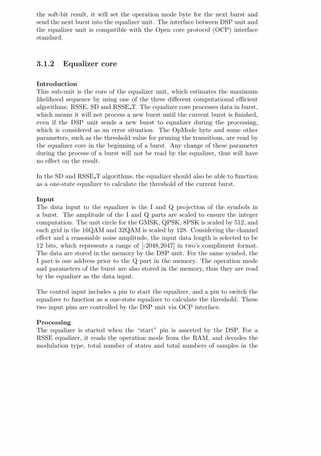
The equalizer unit interfaces with the DSP unit by Open Core Protocol (OCP)interface. The interface implements the basic OCP interface, and it is shown infigure 3.2. Below is a description of each signal in the interface. Most of thedefinition is taken from [13].
����������
������ ��
����������
��������
������� ��
���������
���������
��������������� �����
Figure 3.2: The interface between the DSP and the equalizer unit
MAddr: This is the transfer address set by the DSP unit. The width is config-ured to be 11 to be used according to the data RAM width.
34 Design Specification
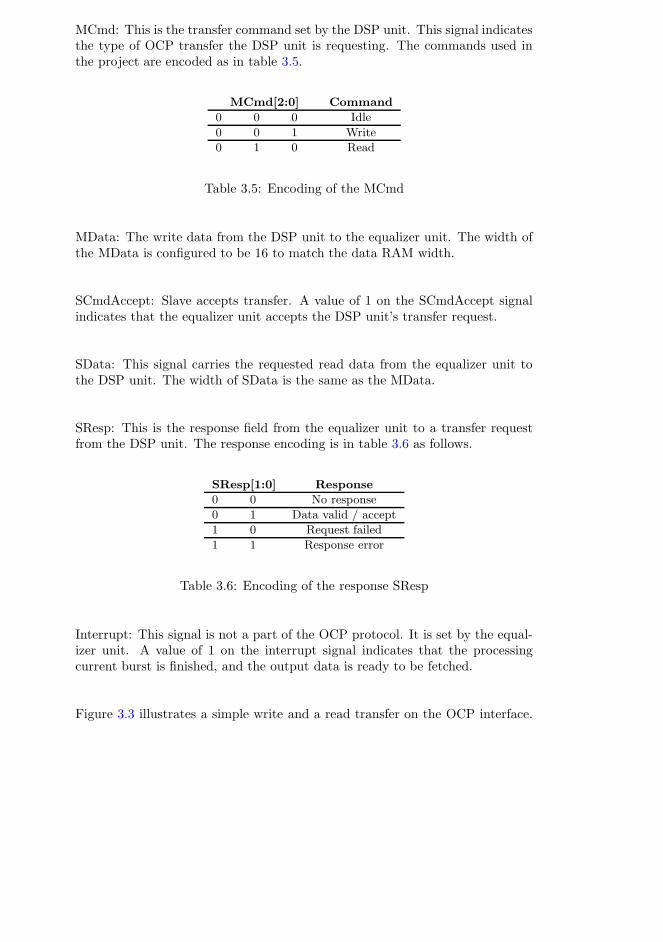
MCmd: This is the transfer command set by the DSP unit. This signal indicatesthe type of OCP transfer the DSP unit is requesting. The commands used inthe project are encoded as in table 3.5.
MCmd[2:0] Command
0 0 0 Idle
0 0 1 Write
0 1 0 Read
Table 3.5: Encoding of the MCmd
MData: The write data from the DSP unit to the equalizer unit. The width ofthe MData is configured to be 16 to match the data RAM width.
SCmdAccept: Slave accepts transfer. A value of 1 on the SCmdAccept signalindicates that the equalizer unit accepts the DSP unit’s transfer request.
SData: This signal carries the requested read data from the equalizer unit tothe DSP unit. The width of SData is the same as the MData.
SResp: This is the response field from the equalizer unit to a transfer requestfrom the DSP unit. The response encoding is in table 3.6 as follows.
SResp[1:0] Response
0 0 No response
0 1 Data valid / accept
1 0 Request failed
1 1 Response error
Table 3.6: Encoding of the response SResp
Interrupt: This signal is not a part of the OCP protocol. It is set by the equal-izer unit. A value of 1 on the interrupt signal indicates that the processingcurrent burst is finished, and the output data is ready to be fetched.
Figure 3.3 illustrates a simple write and a read transfer on the OCP interface.

3.1 Requirements 35
The sequence shown in the figure is described as follows:
1. On clock 1, the master (DSP) starts a request by set the MCmd fieldto Write (WR). At the same time, it presents a valid address (A1) onMAddr and valid data (D1) on MData. The slave (equalizer unit) assertsSCmdAccept in the same cycle.
2. On clock 2, the equalizer captures the values from MAddr and MData anduses them internally to perform the write.
3. On clock 4, the DSP starts a read request by set the MCmd to Read (RD).At the same time, it presents a valid address on MAddr. The equalizerunit asserts SCmdAccept in the same cycle.
4. On clock 5, the equalizer unit captures the value from MAddr and usesit internally to determine what data to present. The equalizer unit startsthe response by switching SResp from NULL to DVA (Data valid), andthen drives the selected data on SData.
5. On clock 6, the DSP recognizes that the SResp indicates data valid andcaptures the read data from SData. This transfer has a request-to-responselatency of 1.
� � � � � � �
�
���
�� �
�����
��� ������
�����
�����
���� �� ���� �� ����
�� ��
��
���� ��� ����
��
Figure 3.3: The waveform of the OCP interface signals
3.1.5 Timing requirements
The timing requirement is that the equalizer should be able to process a burst(at normal symbol rate or high symbol rate) in 1/2 GSM slot time, which is0.577/2 = 0.288 ms, with some margin. The maximum possible clock frequencyis 200MHz.

36 Design Specification
3.1.6 Evaluation Focus
The focus of the project is to compare the power consumption and area cost, aswell as the feasibility of the equalizer cores of various algorithms. The bit errorrate of those algorithms is not a concern in this project.
3.2 Structure Overview
In this section, the structure of the top level equalizer is described. As mentionedin section 3.1, the top level structures of the equalizer of the three algorithmsare very similar. The only difference is that the RSSE algorithm uses a ROMmodule, while the other two algorithms don’t. This section introduces the designof the OCP interface controller, which is used in all three algorithm. The RSSE,SD, and RSSE T main algorithms are implemented in the equalizer core unit,which will be described in the corresponding sections.
The structure of the equalizer unit is shown in figure 3.4.
As shown in the figure, the equalizer unit’s top level consists of a OCP interfacecontroller, a equalizer core, a data RAM, a Surviving symbol memory(Surmem)RAM, and a ROM.
The OCP interface controller allows the DSP unit to communicate with the restof the equalizer unit. The OCP interface controller has access to the data RAM,and it handles all the memory transactions between the DSP and RAM.
The controller interfaces with the equalizer core by three control signals start,done, and one state. When the start signal is asserted, the equalizer core startsto process the input data. When the equalizing process is finished, the equalizercore asserts the done signal. The one state signal is needed to switch the equal-izer core’s mode between normal equalizer (when ’0’) and one-state equalizer(when ’1’).
The equalizer core implements the algorithm to perform the sequence estima-tion. It also has access to the data RAM, since it reads the input burst datafrom the data RAM and writes the output soft-bit to the RAM again. Theequalizer core has also access to the Surmem RAM, which stores the survivingsymbols for the trellis search. A ROM structure is connected to the equalizercore. The ROM stores the initial Surmem elements.

3.3 OCP interface controller 37
�������������
����������
�����
���������
���������
����������
��������
���������
���������
��������
�������
� ��!"#��
����
�
�
�
�
�
�
�
�
�������
��
$�
����"�����
�����������
�����
���
�����
����������
����%������
����$ �
������
�����������
����������
����$ �
������
�����������
����%������
�����������
����������������
������%��
������%��$ �
������%����
������%����������
��������$�
����������
&���������
&���
&�'�
&�����"����
&��������
&��
&'�
&����������
����������
����(���
�%�
%�&("����)���
������!!��
���
���
�*(���
&
�
&
�������������
%�������
%�!+()��(����(�!,��"�-�
�����
Figure 3.4: The structure of the equalizer unit
The data RAM is a single port synchronous RAM of 64kb. The Surmem RAMis a dual port synchronous RAM of 64kb. These two RAMs are not physicalcells, but simulation models generated by Denali Software Pureview instead.The ROM is of 8kb, and is implemented as a constant array. The ROM is notneeded in the SD and RSSE T algorithms.
3.3 OCP interface controller
As mentioned in the section 3.2, the OCP interface controller is the interfacebetween the DSP and the data RAM, as well as the interface between the DSPand the equalizer core. It performs the arbitration of data RAM access betweenDSP and equalizer data path. Besides, the controller also controls the sequence
38 Design Specification
of processing a burst.
The OCP interface standard has been described in section 3.1.4. Besides theOCP interface, the controller should also interpret the request from the DSPinternally, and gives data RAM access to DSP.
The physical interface is implemented in the following way: The MData, SDataand MAddr is connected directly to the DataIn, DataOut and DataAddr of theRAM. And the controller controls the RAM access by switching the CE andWE signals.
The interpretation of the DSP request is stated below, and an example showingthe waveform of the interface between DSP and RAM is in figure 3.5.
• When the MAddr is 0x00, and MCmd is ”Write”, the MData containsan command word that will be written into a internal command registerin the controller (Cmd reg[7:0]). Only the two LSB’s of the command isused. A ’1’ of Cmd reg[0] sets the equalizer unit in slave mode and theDSP has full access to the data RAM. A ’0’ of Cmd reg[0] means theDSP releases the control of the data RAM. The equalizer then works inthe master mode and the equalizer core may access the data RAM. A ’0’of Cmd reg[1] bit switch the equalizer core to be the one-state equalizer,while a ’1’ sets the core to function as a normal equalizer. This commandfrom the DSP is stored in a register, and will not be changed until theDSP sends a new command at MAddr 0x00. This situation is shown infigure 3.5 clock 1 and 6.
• When the MAddr is other than 0x00, and the MCmd is ”Write”, thecontroller should write data to the RAM. It simply asserts both the CEand the WE signal of the RAM. Since the MAddr and MData is connecteddirectly to the address bus and data in bus of the RAM, the data on theMData bus will be written immediately to RAM at the address on theMAddr bus. This situation is shown in figure 3.5 clock 2 and 3.
• When the MAddr is other than 0x00, and MCmd is ”Read”, the MAddrcontains the address of the RAM the DSP unit tries to access. The con-troller should immediately perform an Read action of the RAM by assert-ing the CE signal. After the latency of the read action of RAM, the RAMdrives the required data on the data bus, which is connected directly tothe SData bus. This situation is shown in figure 3.5 clock 4 and 5.
The sequence of processing a burst is controller by the OCP interface controller.The controller should
3.3 OCP interface controller 39
� � � � � � �
�
���
�� �
�����
�����
���� �� �� �� ����
� ���
����
����
� � ���
���� ����
������ ����
��
�
�
����
���� ����
����
� ���� � ��� �
���� ���� ���� ����
���� ���������
����!"�
� �
��
��
� ���#�$�%�&%���
� ���#�$�%�&%��'
Figure 3.5: The waveform of the controller interfacing DSP to RAM
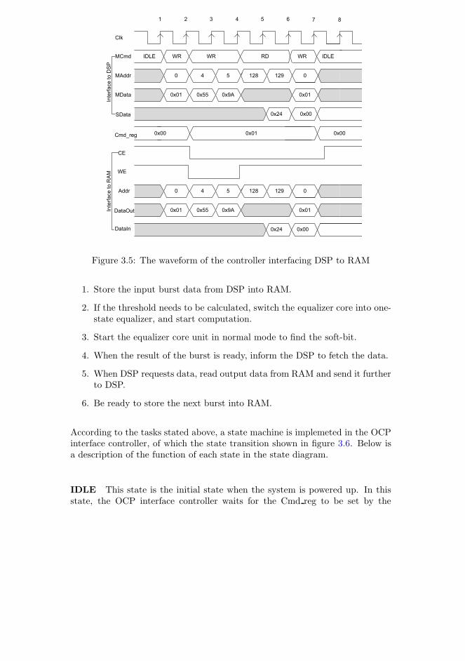
1. Store the input burst data from DSP into RAM.
2. If the threshold needs to be calculated, switch the equalizer core into one-state equalizer, and start computation.
3. Start the equalizer core unit in normal mode to find the soft-bit.
4. When the result of the burst is ready, inform the DSP to fetch the data.
5. When DSP requests data, read output data from RAM and send it furtherto DSP.
6. Be ready to store the next burst into RAM.
According to the tasks stated above, a state machine is implemeted in the OCPinterface controller, of which the state transition shown in figure 3.6. Below isa description of the function of each state in the state diagram.
IDLE This state is the initial state when the system is powered up. In thisstate, the OCP interface controller waits for the Cmd reg to be set by the

40 Design Specification
����
�����
�� ����
��
���������
������
���������� ��
���������� � �
���������� ��
�������� !�� ��"��#
��������
�������
���������� ��
���������� ���
$��������
�� ����
�������� !�� ��" �#
�������
��������
Figure 3.6: The state diagram of the OCP interface controller
DSP unit. When the DSP sets the Cmd reg(0) to ’1’, the control moves tothe RAM TRANSACTION state and starts the equalizing process. Duringequalizing process, the system will not enter this IDLE state again.
RAM TRANSACTION This state handles the Read/Write process by theDSP unit. In this state, the DSP unit has full access to the RAM, and theequalizer unit works in slave mode. The DSP first reads out the result of theprevious burst, and then writes a new burst to the RAM. When the DSP unitfinishes the read/write access to the RAM, it sets the Cmd reg[0] to ’0’. Thecontroller enters the NORMAL EQUALIZER state if the Cmd reg[1] is ’1’, orthe ONE STATE EQUALIZER state, if the Cmd reg[1] is ’0’.
NORMAL EQUALIZER In this state, the equalizer unit works in mastermode. The controller starts the equalizer core by asserting the start signal. Theequalizer core has the full access to the data RAM in this state. When thecore finishes processing one burst of data, it asserts the done signal, and thecontroller enters the WAIT END state.
3.4 RSSE Equalizer core 41
ONE STATE EQUALIZER This state is used for calculating the thresholdvalue of the trellis structure. The controller in state functions the same as inthe NORMAL EQUALIZER state. It asserts the start signal and the one statesignal to start the equalizer in one-state equalizer mode, and waits for the donesignal to be asserted by the equalizer core. When this state ends, the controllerassumes the threshold value has been calculated. Then it will always enterthe NORMAL EQUALIZER state. This state should always be skipped inthe RSSE equalizer by keeping the Cmd reg[1] to be ’1’, since no thresholdcalculation is needed.
WAIT END In this state, the controller asserts the interrupt signal to informthe DSP to fetch the soft-bit result. Then it waits for the DSP to request data.When DSP unit sets the Cmd reg[0] to ’1’, the controller leaves this state andenters the RAM TRANSACTION state.
3.4 RSSE Equalizer core
3.4.1 Structure overview
This equalizer core implements the RSSE algorithm (refered to as RSSE equal-izer below). The structure design of the RSSE equalizer is shown in figure 3.7.
A brief description of the submodules and their function is as followed:
Channel symbol LUT This module implements the inner product of thechannel impulse response with the Surmem elements. The Surmem elements,together with the input of the modulation type, select a value from the lookuptable which stores the multiplication result of the channel impulse responsewith the complex representation of the symbols. Six values from the LUT areselected, and the sum of these six value is the output of this module. Thismodule implements the summation part of equation 2.10.
Error Calculation This module takes the modulation type and the decisionvariables calculated as in equation 2.10 as input. Then it calculates the dis-tance(squared error) of the decision variable to each of the reference point onthe constellation diagram. The squared error to each point is the output of this
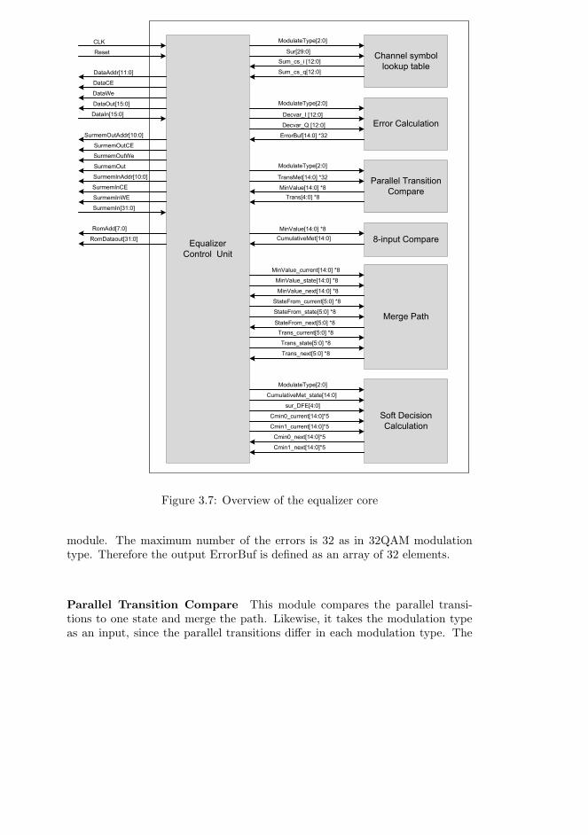
42 Design Specification
���
�����
���
����
� ����� �
� ����� ��
� ����� ���
� �������
� ��������
��������������
���� ������
���������
��������� �����
������� ���������
������
!"��� ��������
��#�����������
��� �����
�$ ��%��
���������&���
��' ��� ���()*+,
� �()-*+,
� �.��.��(/)*+,
� �.��.$(/)*+,
������ �(0/*+,
���1''(2*+,
����(/3*+,
��� �(/3*+,
��1''�(//*+,
� ������(0/*+,
� ������1''�(/+*+,
� ����� �1''�(/+*+,
��' ��� ���()*+,
���4�.��(/)*+,
���4�.5�(/)*+,
�����6 #(/7*+,�80)
��' ��� ���()*+,
������(/7*+,�80)
���9� �(/7*+,�8!
���(7*+,�8!
���9� �(/7*+,�8!
� � ���4����(/7*+,
���9� �.��:�(/7*+,�8!
���9� �.����(/7*+,�8!
���9� �.� �����(/7*+,�8!
����;���.� �����(3*+,�8!
����;���.����(3*+,�8!
����;���.��:�(3*+,�8!
���.� �����(3*+,�8!
���.����(3*+,�8!
���.��:�(3*+,�8!
� � ���4����.����(/7*+,
��' ��� ���()*+,
� �.�;�(7*+,
����+.� �����(/7*+,83
����/.� �����(/7*+,83
����+.��:�(/7*+,83
����/.��:�(/7*+,83
Figure 3.7: Overview of the equalizer core
module. The maximum number of the errors is 32 as in 32QAM modulationtype. Therefore the output ErrorBuf is defined as an array of 32 elements.
Parallel Transition Compare This module compares the parallel transi-tions to one state and merge the path. Likewise, it takes the modulation typeas an input, since the parallel transitions differ in each modulation type. The
3.4 RSSE Equalizer core 43
other input, TransMet, stores the path metric value, which is the sum of the reg-istered ErrorBuf value from the Error Calculation module and the state metricof the current state. The parallel transition are merged by choosing the mini-mum value of the path metric that have the same destination state, and storedin the output array: MinValue, and the transition associated to this minimumvalue is stored into another output array: Trans. Together they are the outputof this module. The maximum number of MinValue is 8, so the output arearrays of 8 elements.
Merge Path This module compares and merges the path of different trellisstates that needs to be merged. It compares the array which stores the currentminimum metric MinValue currrent, with the registered MinValue result (Min-Value state) from the Parallel Transition Compare, which is the metric of thecurrent state. The eight values in the array MinValue state represent the metricof the path going to eight destination states, and they should be compared withthe corresponding metric in the array MinValue current that has the same des-tination state. The minimum value after the comparison is stored into the arrayMinValue next, and the registered MinValue next is the new MinValue currentinput of the next clock cycle. Likewise, the transitions associated to the mini-mum value are stored into the Trans next array, and the source states associatedto the minimum value are stored into the StateFrom next array. When no morepaths need to be merged for these destination states, the MinValue next resultwill be stored as the state metric of the destination state in the next stage. TheTrans next and the StateFrom next will be saved into the register files and usedfor updating the Surmem of the next stage.
8-input Compare This module takes the registered MinValue output fromthe Parallel Transition Compare module as the input, and finds the minimumvalue among these MinValue. This value is called CumulativeMet and will beused as the input for the Soft Decision Calculation module.
Soft Decision Calculation This module calculates the soft-bit result accord-ing to the modulation type, the CumulativeMet from 8-input compare module,the surviving symbol memory element, and the registered temporary soft-bitresult. This module implements the equation 2.26, and calculates the soft-bitdecision from the input signals. The output signals are the temporary soft-bitresult Cmin0 next and Cmin1 next of the current state. The output will beregister and used as the input for the next clock cycle. When all the states inthe trellis structure have been calculated, the result will be saved as the soft-bitresult for the current stage.

44 Design Specification
3.4.2 State diagram
A state machine is implemented in the equalizer’s controller unit. The statemachine handles the memory read and write, and sends the control signal tothe data path according to the RSSE algorithm. The state diagram is shown infigure 3.8, and the operations the controller performs in each state are explainedbelow.
����
������
�� ����
�����
�� �
����
������ �
��������
��������
��������
� ��
����
�������
� �� ����
� �� ����
�� � ��� � �!"
�� � ��� � �!"
���
�� � ��� � �
�� � ��� � �!"
������ � �������
������� �#�!$��%&��'�
��(� �����)$��
�� � ��� � �!"
��(� �����)$��
�� � ��� � �
�� � ��� � �!"
������ � �������
������� �#�!$��%&��'�
��"
��"
Figure 3.8: The state diagram of the RSSE equalizer
IDLE The controller unit is in the state when the system is powered up, orwhen it finishes processing a burst of data. The controller waits in this stateuntil the top level controller asserts the start signal. And it will go to the stateREAD PARAMETER.
READ PARAMETER In this state, the controller reads the operation modecontrol byte stored in the data RAM and decodes the byte. The modulationtype, total number of states used in the trellis structure, and total number ofsamples in the burst are stored into the registers. Since the data RAM is a syn-chronous RAM, it will drive the data on the data bus in the next clock cycle.

3.4 RSSE Equalizer core 45
The input data from the RAM is stored in a register, so one more clock cycle isneed for the controller to get the data. A counter i is used to record the numberof the times the state is executed. After 3 clock cycles, the data is obtained anddecoded, the controller moves on to the LOAD ROM state. The controller onlyenters this state before it processes the first sample of each burst.
LOAD ROM The controller load the initial Surmem elements from the ROMaccording to the Modulation type and total states it decoded in the READPARAMETER state. If N states in the trellis are required, the state will loop
for N clock cycles. Each clock it reads out 6 elements for the same trellis state,and stores them into a certain address in the Surmem RAM. When all theinitial Surmem elements have been loaded into the RAM, the controller entersthe READ DATA state. Same as the READ PARAMETER state, this state isonly executed before the burst samples are processed.
READ DATA In this state, the controller reads the I and Q of the currentprocessed sample from the data RAM, and stores them into the registers. Thisstate starts the trellis calculation for each stage. Since two addresses in the RAMhave been read, the state will be executed for four times to get the required data.
READ SURMEM This is the state where most of the calculation is takingplace. Depending on the total trellis state N, the state will be executed for Nclock cycles. Each time it reads out six Surmem elements associated to onetrellis state and inputs them into the data path. The data path performs pathextension and merging for a new trellis state at each clock cycle. The trellisstates have further been grouped into blocks. The states in the same block havethe same sequence of destination state, therefore in-block merging is performed.When the controller finishes calculating one block, it sends out a control signalto store the path merging result into register files. After N clock cycles, thecontroller assumes that all the trellis state have been calculated, and it entersthe PIPELINE OVERHEAD state.
An overview of the number of block and block size in each modulation types areshown in the table 3.7.
PIPELINE OVERHEAD The data path of the equalizer core is pipelinedinto 7 stages to increase the throughput of the critical path. Due to the pipeline,the data path will have a latency of 6 clock cycles. When N trellis states arecalculated in the data path, a N+6 clock cycles are needed for pipe-cleaning.
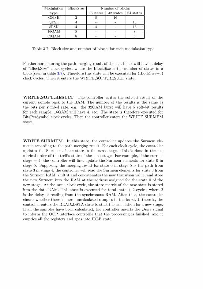
46 Design Specification
Modulation BlockSize Number of blockstype 16 states 32 states 64 states
GMSK 2 8 16 -
QPSK 4 - - 16
8PSK 4 4 - 16
16QAM 8 - - 8
32QAM 8 - - 8
Table 3.7: Block size and number of blocks for each modulation type
Furthermore, storing the path merging result of the last block will have a delayof “BlockSize” clock cycles, where the BlockSize is the number of states in ablock(seen in table 3.7). Therefore this state will be executed for (BlockSize+6)clock cycles. Then it enters the WRITE SOFT RESULT state.
WRITE SOFT RESULT The controller writes the soft-bit result of thecurrent sample back to the RAM. The number of the results is the same asthe bits per symbol rate, e.g. the 32QAM burst will have 5 soft-bit resultsfor each sample, 16QAM will have 4, etc. The state is therefore executed forBitsPerSymbol clock cycles. Then the controller enters the WRITE SURMEMstate.
WRITE SURMEM In this state, the controller updates the Surmem ele-ments according to the path merging result. For each clock cycle, the controllerupdates the Surmem of one state in the next stage. This is done in the nu-merical order of the trellis state of the next stage. For example, if the currentstage = 4, the controller will first update the Surmem elements for state 0 instage 5. Supposing the merging result for state 0 in stage 5 is the path fromstate 3 in stage 4, the controller will read the Surmem elements for state 3 fromthe Surmem RAM, shift it and concatenates the new transition value, and storethe new Surmem into the RAM at the address assigned for the state 0 of thenew stage. At the same clock cycle, the state metric of the new state is storedinto the data RAM. This state is executed for total state + 2 cycles, where 2is the delay of reading from the synchronous RAM. After that, the controllerchecks whether there is more uncalculated samples in the burst. If there is, thecontroller enters the READ DATA state to start the calculation for a new stage.If all the samples have been calculated, the controller asserts the Done signalto inform the OCP interface controller that the processing is finished, and itempties all the registers and goes into IDLE state.

3.4 RSSE Equalizer core 47
3.4.3 Timing analysis
���������������� �
���� ����
���
���
��������������������� �� ��
������� ������ ���� ��� �
�����
���
���������������� �
���������������� �
���������������� �
���������������� �
���������������� �
������ ��������
���������������� ��
������ ��������
������ ��������
���������������� ��
������ �������!
���
������
Figure 3.9: Pipelining the process of the RSSE controller
The figure 3.9 shows the pipeline organization at any trellis stage when process-ing a 32QAM burst. In the figure, each trellis state has a throughput of oneclock cycle, and the storage of the first block starts at BlockSize + PipelineStage- 1 clock cycle. The total clock cycles needed for processing a stage (exclusiveread/write from RAM) is 64 + 8 + 6 = 78 cc. The computation time of theentire burst can also be estimated. Here the worst case, a high symbol rate32QAM of 171 samples, is calculated. Adding the clock cycles for each state inthe state diagram.
3 + (64 + 2) + [4 + 78 + 5 + (64 + 2)] ∗ 171 = 26232cc
When using the clock with the maximum frequency = 200MHz, the clock periodis 5ns, and the computation time is
26232 ∗ (5 ∗ 10−9) = 131µs < required 577/2 µs
48 Design Specification
If comparing the computation time with the timing requirements, it can be seenthat the design holds the timing requirements. In fact the design only occupieshalf of the maximum allowed time, which makes it possible to optimize the areaby decreasing the use of the parallelism. However, this approach is not carriedout in this project.
3.4.4 Module design
The data path of the RSSE equalizer is shown in figure 3.10. The data path is7-stage pipelined, as to increase the throughput of the critical path.
The data path is designed according to the algorithm described in section 2.6.3.The pipeline stage 0 is store the input data and Surmem elements into registers.The pipeline stage 1 implements the summation part in equation 2.10. Thepipeline stage 2 implements the rest part of equation 2.10. The pipeline stage3 implements equations 2.12 to 2.15. The pipeline stage 4 merges the paralleltransition, and together with stage 5, they implement equations 2.18 to 2.21.Stage 6 implements equation 2.26.
It can be seen that the clock-gating is applied on the equalizer by propagating anenable signal along the data path. The pipeline register stalls when the enableis ’1’. In this way, the unwanted switching activities will not be performed bythe data path.
The modules shown in the data path are implemented as combinatorial logics.All the input and output signals of the modules are registered in the controller’spipeline registers. This approach makes it easy to modify the RSSE equalizerinto an equalizer using another algorithm, simply by replacing modules in thedata path.
Below is a description of the hardware implementation of each module in thedata path.
3.4.4.1 Channel symbol LUT
This module uses the Surmem memory elements as well as the modulation typeas the index to search for the required channel symbols, as shown in figure 3.11.
The look-up table is implemented as a pre-calculated constant array. Each

3.4
RS
SE
Eq
ua
lizerco
re4
9
���������
��������
������
����������
��������
��������
�
��������
�������
�����
������
�����
��������
��������
�������������
������������
�
�
�
�
�
���
��
!��
����������
�
�
�
�
�
������������
!����������"#$�%
!��������
!��������
�������������
&
'()�����
��������
��������������"#$�%
���* �*�
!������
�����
+�������
������������
��������������, ��������������& ��������������- ��������������. ��������������/
!������������
��
����01�
���������
�������
�2����34! �
������*������
'
&
���"�$.%
��������������
����
01�
���������������
' ,
'
'
/
&, '
155�
����
155�
&�
'
.
'
' .
.
'
.6(
'
/
'
'
.
.6 �
'
'
.6.
'
/
.6/-
'
.6(
'
.6(
'
'
.6(
/6(
'
.6(
'
.6/-
'
/6/-
'
����������������� ��������, ��������& ��������- ��������.
��������/
��������.
Fig
ure
3.1
0:
Th
ed
ata
path
of
the
RS
SE
equ
alizer

50 Design Specification
�����������
���
���
���
���
���
���
�
�
�
�
�
�
�
�
�
�
�
�
� �
�����������
�
������� �!
���"�� �!
��#$
�
��#$
�
��%����"
��%�����
��
�
��
�
Figure 3.11: Channel symbol LUT module
address contains 6 integer numbers of 11 bits each, representing a range of [-1024,1023]. The pre-calculation is to multiply the channel impulse responsewith the complex representation of the constellation point. The result is anarray of six complex numbers, called six channel symbols. The real part of thesix channel symbols are saved at one address of the look-up table, and imaginarypart are saved at the next address. Figure 3.12 illustrates the contents of thefirst few addresses in the LUT. From the figure, the real part of the channelsymbols of symbol 0 are saved at address 0, while the imag part are saved ataddress 1. The real part of the channel symbols of symbol 1 are saved at address2, while the imag part are saved at address 3. The GMSK channel symbol look-up table is followed by the QPSK channel symbol table etc., in the memoryspace.
����
����
��
��
� �� � � �� �
�
�
�
��� �� ��� ��� �� ��
������
��
����
����
����
� ���
Figure 3.12: The data organization in the look-up table
When the controller sends an array of Surmem elements of one trellis state, theelements are used to select in the look-up table. E.g. when the modulation type
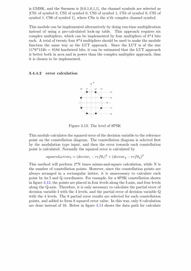
3.4 RSSE Equalizer core 51
is GMSK, and the Surmem is [0,0,1,0,1,1], the channel symbols are selected as[CS1 of symbol 0, CS2 of symbol 0, CS3 of symbol 1, CS4 of symbol 0, CS5 ofsymbol 1, CS6 of symbol 1], where CSn is the n’th complex channel symbol.
This module can be implemented alternatively by doing run-time multiplicationinstead of using a pre-calculated look-up table. This approach requires sixcomplex multipliers, which can be implemented by four multipliers of 8*4 bitseach. A total of twenty four 8*4 multipliers should be used to make the modulefunction the same way as the LUT approach. Since the LUT is of the size11*6*124b = 8184 hardwired bits, it can be estimated that the LUT approachis better both in area and in power than the complex multiplier approach, thusit is chosen to be implemented.
3.4.4.2 error calculation
�� �� �� ��
��
��
��
��
�
�
Figure 3.13: The level of 8PSK
This module calculates the squared error of the decision variable to the referencepoint on the constellation diagram. The constellation diagram is selected firstby the modulation type input, and then the error towards each constellationpoint is calculated. Normally the squared error is calculated by
squared error0 = (decvari − ref0i)2 + (decvarq − ref0q)
2
This method will perform 2*N times minus-and-square calculation, while N isthe number of constellation points. However, since the constellation points arealways arranged in a rectangular lattice, it is unnecessary to calculate eachpoint by its I and Q coordinates. For example, for a 8PSK constellation shownin figure 3.13, the points are placed in four levels along the I-axis, and four levelsalong the Q-axis. Therefore, it is only necessary to calculate the partial error ofdecision variable I with the 4 levels, and the partial error of decision variable Qwith the 4 levels. The 8 partial error results are selected for each constellationpoints, and added to form 8 squared error value. In this way, only 8 calculationare done instead of 16. Below in figure 3.14 shows the data path for calculate

52 Design Specification
the error of decision variable I with level L0, and decision variable Q with levelL0. In the Error Calculation module, 6 of these units shown in figure 3.14 areused, and they form a maximal of 32 squared error outputs.
����������
��
�
�
�
�
����
�
�
����������
��
�
�
�
�
����
�
���������
��������
Figure 3.14: The error calculation unit, one set of error
The diagram of the complete module is shown in Appendix B figure B.2.
3.4.4.3 Parallel Transition Compare
The output from the Error Calculation module is organized in a way thatthe error to the points of the same subset of set-partitioning is placed to-gether. For example, the constellation points of the 8PSK is set-partitionedas [(0,4),(1,5),(2,6),(3,7)], and the output array ErrorBuf from the Error Calcu-lation is ErrorBuf(0 : 7) = [Err0, Err4, Err1, Err5, Err2, Err6, Err3, Err7],and the rest the of the ErrorBuf is all 1’s (maximal value). Then the comparisonis carried out within the subset, which in this example is Err0 with Err4,Err1
with Err5, etc. The symbol is passed as the parameter of the comparison. Thesmaller one is kept as the output. The comparison unit for the subset (0,4) isshown in figure 3.15.
In 32QAM, the points are set-partitioned into 8 subsets with 4 points each.Therefore the 4 points are compared two and two by using two of the compar-ison units shown in figure 3.15, and the results are compared again using onecomparison unit. A total of 24 comparison units are required for the 32QAM,and the result is 8 path merging survivors, each to a different destination state.
While the burst of modulation types with smaller alphabet, like 16QAM and8PSK, is calculated, not all the comparison units are required. The input tothe unused logics remain unchanged during the processing to avoid switchingactivity by applying operand-isolation.

3.4 RSSE Equalizer core 53
�
�
����
�
�
�
�
�
�
��������
��
�
����������
������
��
���
Figure 3.15: The comparison unit with one parameter
For QPSK and GMSK, there is no set-partitioning performed on the symbolset, and thereby no parallel transition. The module should be passed through.
The diagram of this module is shown in Appendix B figure B.3.
3.4.4.4 Merge Path
The Merge Path module compares and merges the path of different trellis states.The input to the module is two arrays, MinValue state(0:7) and Trans state(0:7),containing the parallel transition merge result and the current trellis statenumber, respectively. They are compared with the current minimum met-ric array, MinValue current(0:7). The comparison is done in a way such thatMinValue state(0) is compared with MinValue current(0), MinValue state(1) iscompared with MinValue current(1),etc. The comparison for one path metricis shown in figure 3.16. Supposing the MinValue state(0) is smaller, it willbe stored in MinValue next(0). Its transition Trans state(0) will be stored inTrans next(0), and the current trellis state number will be stored in State-From next(0). Otherwise the MinValue current and its parameters are stored.One clock cycle later, the “ next” signals is stored into the registers “ current”,and used to compare with the metric of the next trellis state.
The controller sends a signal write en to indicate if the merge process is finished.And if the signal is asserted, the MinValue next, Trans next,and StateFrom nextare written in the register files MinValue buf, Trans buf, and StateFrom buf re-spectively. The register “ current” are cleared for next block of merging process.This will be introduced in details in the section 3.4.4.7 book-keeping mechanism.
A total of 8 units shown in figure 3.16 are used in the module. Only the logicsinside the box in the figure are the logics in the module. The logics outside the
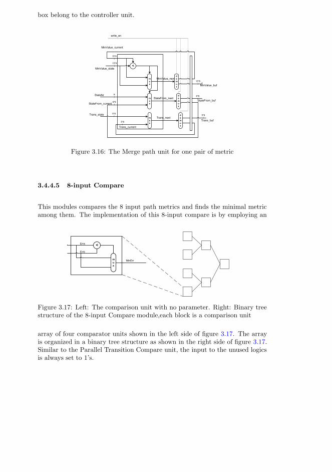
54 Design Specification
box belong to the controller unit.
�
�
�
�
�
�
�
��������������
��������������
�������������
������
�����������
�����������
�
�
�
�����������
����������
�
�
�
�
�
�
�
�
�
�
�
�
�
�
�
�������
��������
����
�
����
�
�
�
���
�
����
�
���
�
���
�
���
�
���
����������
������������
������������
Figure 3.16: The Merge path unit for one pair of metric
3.4.4.5 8-input Compare
This modules compares the 8 input path metrics and finds the minimal metricamong them. The implementation of this 8-input compare is by employing an
�����
����
�
�
�
������
Figure 3.17: Left: The comparison unit with no parameter. Right: Binary treestructure of the 8-input Compare module,each block is a comparison unit
array of four comparator units shown in the left side of figure 3.17. The arrayis organized in a binary tree structure as shown in the right side of figure 3.17.Similar to the Parallel Transition Compare unit, the input to the unused logicsis always set to 1’s.

3.4 RSSE Equalizer core 55
3.4.4.6 Soft Decision Calculation
This modules calculates the soft-bit decision. The input is taken from the 8-input compare module’s output. As described in the previous chapters, Thesoft decision is made for the transmitted symbol from the N th-previous stage,where N is decided by the modulation types and the total states. The controllersends this transmitted symbol SurDFE to the module, and the bit format ofthe symbol is found by using a bit format LUT. If symbol contains 5 bits, 5units shown in figure 3.18 are used in the module. The BitN indicates whichbit in the symbol is calculated. Each unit compares the input minimum metricwith Cmin0 current, if the bit is 0, or with Cmin1 current, if the bit is 1. Theminimum value of the comparison are stored, and used as the compare valueCmin0 current or Cmin1 current for the next state.
���������
����� ����
������
�� ���
������
�� ���
�
�
�
�
�
�
�
������������
�����
�
�
�
�
�
�� �������������
�
�� ����
�
��
�
��
�
��
�
��
�
���
��
������
����
������
����
Figure 3.18: The Soft Decision Calculation unit
3.4.4.7 Book-keeping Mechanism
The trellis structure used in the project has the characteristics that the states inthe same block have the same destination states. The example shown in figure3.19 is a 16-state 8PSK trellis structure, separated into 4 blocks. From thefigure, it can be seen that all the states in the first block have the destinationstates of the first state in four blocks.
This trellis structure requires an advanced book-keeping mechanism, since thepath metric, source state, etc, of the destination state are not calculated in thenumerical order. In the example in figure 3.19, the sequence of the calculation

56 Design Specification
of the destination states are: (0,4,8,12), (1,5,9,13),(2,6,10,14),(3,7,11,15), witheach set (shown in the bracket) computed at the end of the block.
Figure 3.19: The trellis structure of 8PSK 16 state modulation type in blocks
Basically two register files are used for the book-keeping mechanism: one usedfor the temporary path merging result inside a block (Block Registers), and oneto store the result of the stage(Stage Register Files). The Block Registers have8 entries, and are cleared when the calculation of a block finishes. The StageRegister Files have 64 entries, and are cleared at the end of each stage.
The book-keeping mechanism is closely related with the Merge Path mod-ule. The output from the Merge Path module are stored into the registers:Min metric current, Trans current, and StateFrom current, as shown in figure3.16. These are the actual content of the Block Registers’ entry. Each of themcontains a maximum of 8 elements going to 8 different destination states. Whenthe computation of a block is finished, the Block Registers are written into theState Register Files directly. A pre-calculated destination state value (StateTo)is added to each entry of the State Register Files. As shown in the example infigure 3.20, for the first block, the 4 entries in the Block Registers are writteninto the first four entries of the Stage Register Files. For the next block, theBlock Registers will be written into the next 4 entries of the Stage RegisterFiles.
When the calculation for a stage is finished, the data in the Stage Register Filesare written into the RAM. Since the data in RAM are placed according to theirstate number, the StateTo signals are used to calculate the destination state.
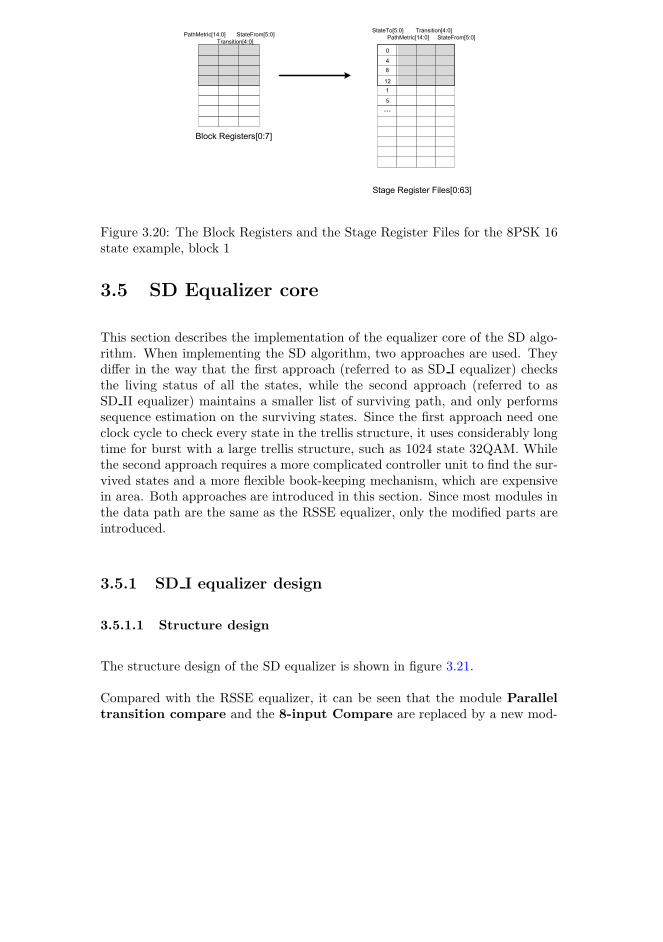
3.5 SD Equalizer core 57
����������� ������
������ �������
� �����������
������� �������
���������� ��������� �
������� �������
� �����������
������ �������
������������
�
�
!
�"
�
###�
Figure 3.20: The Block Registers and the Stage Register Files for the 8PSK 16state example, block 1
3.5 SD Equalizer core
This section describes the implementation of the equalizer core of the SD algo-rithm. When implementing the SD algorithm, two approaches are used. Theydiffer in the way that the first approach (referred to as SD I equalizer) checksthe living status of all the states, while the second approach (referred to asSD II equalizer) maintains a smaller list of surviving path, and only performssequence estimation on the surviving states. Since the first approach need oneclock cycle to check every state in the trellis structure, it uses considerably longtime for burst with a large trellis structure, such as 1024 state 32QAM. Whilethe second approach requires a more complicated controller unit to find the sur-vived states and a more flexible book-keeping mechanism, which are expensivein area. Both approaches are introduced in this section. Since most modules inthe data path are the same as the RSSE equalizer, only the modified parts areintroduced.
3.5.1 SD I equalizer design
3.5.1.1 Structure design
The structure design of the SD equalizer is shown in figure 3.21.
Compared with the RSSE equalizer, it can be seen that the module Paralleltransition compare and the 8-input Compare are replaced by a new mod-
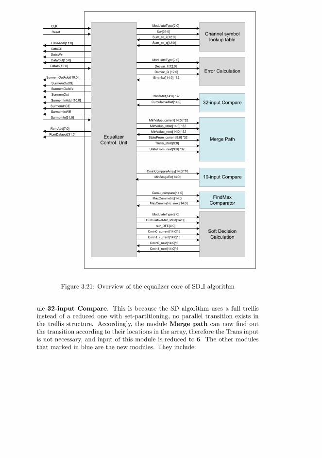
58 Design Specification
���
�����
���
����
� ����� �
� ����� ��
� ����� ���
� �������
� ��������
��������������
���� ������
���������
��������� �����
!"��� ��������
��#�����������
��� �����
�$ ��%��
���������&���
��' ���(���)!*+,
� �)!-*+,
� �.��.��)/!*+,
� �.��.$)/!*+,
������ �) /*+,
���0'')1*+,
����)/2*+,
��� �)/2*+,
��0''�)//*+,
� ������) /*+,
� ������0''�)/+*+,
� ����� �0''�)/+*+,
��' ���(���)!*+,
���3�.��)/!*+,
���3�.4�)/!*+,
�����5 #)/6*+,�7 !
(������)/6*+,�7 !
� � ���3����)/6*+,
���8� �.��9�)/6*+,�7 !
���8� �.����)/6*+,�7 !
���8� �.� �����)/6*+,�7 !
����:���.� �����)-*+,�7 !
(������.����)-*+,�
����:���.��9�)-*+,�7 !
����������0���)/6*+,7/+
� � .������)/6*+,
�9� �������)/6*+,
� � ���3����.����)/6*+,
��' ���(���)!*+,
� �.�:�)6*+,
����+.� �����)/6*+,72
����/.� �����)/6*+,72
����+.��9�)/6*+,72
����/.��9�)/6*+,72
:��'�9
��������
/+"��� ������������������)/6*+,
�9� �������.��9�)/6*+,
Figure 3.21: Overview of the equalizer core of SD I algorithm
ule 32-input Compare. This is because the SD algorithm uses a full trellisinstead of a reduced one with set-partitioning, no parallel transition exists inthe trellis structure. Accordingly, the module Merge path can now find outthe transition according to their locations in the array, therefore the Trans inputis not necessary, and input of this module is reduced to 6. The other modulesthat marked in blue are the new modules. They include:
3.5 SD Equalizer core 59
• 32-input Compare: This module is to replace the module Paralleltransition compare and 8-input compare. It simply combines the2-stage comparators in the module Parallel transition compare andthe 3 stage comparators in the module 8-input compare together, andmakes a 5-stage binary tree structure with comparators with 1 parameter,as shown in figure 3.15.
• 10-input Compare: This module is very similar to the module 32-inputCompare. It compares the ten elements in the input array in a paralleledway. It has a tree structure similar to the 8-input compare, of whicheach stage contains 5-2-1-1 comparators as shown in 3.17. This module isused to compare among the soft-bit decisions to find the cumulative errorof the stage.
• Findmax Compare: This is a single comparator similar as shown in 3.17with a opposite bigger-than operator. The module is used by the one-statetrellis to find out the maximal error of the stages.
The data path of the SD I equalizer is shown in figure 3.22. The difference withthe data path of RSSE equalizer is that there are 6 pipeline stages instead of 7,and new modules introduced above are plugged into the data path.
Although the structure and data path of the SD I equalizer are similar to theRSSE equalizer, the controller design is very different. One major difference isthat an one-state equalizer is designed to find the maximum stage error of theburst. The section below introduces the design of the one-state equalizer.
3.5.1.2 One-state equalizer
The SD equalizer should be able to function as a one-state equalizer. Sinceone-state equalizer can be taken as a special form of the normal equalizer, itshould be possible to reuse the data path with some different control signals.If the one-state equalizer is configured, the state machine goes into a differentsequence than the normal equalizer. The state diagram is shown in figure 3.23.
The IDLE state, the READ PARAMETER state, and the READ DATA stateare the same as in the RSSE state machine. The new states are:
ONE STATE EQUALIZER This state controls the most part of data pro-cessing. It captures the Surmem elements sent by the RAM, and feeds them

60
Desig
nS
pecifi
catio
n
�������
�������
� ����
���������� �
�������������
���
����������
�������
�������
�
��������
������
��!��
��� �����
�"��
�������
��#�"
�����������
�����"�����"
�
�
�
�
����$
���%
���
�������
�
�
�
�
�
�����"�������
���
�����������"
&
%'
&
%'
�($)*+
',-�����
�������
�
�����
����
������
�����
. �����
�����������
/����������!��% /����������!��, /����������!��' /����������!��0 /����������!��*
����������
��� ����
���
/����������!��$
�
�
�
%1�
�
�
�
�
�
2�3��4
��������
�������
�������
�����!�$ �����!�% �����!�, �����!�'�����!�0
�����!�0
�����!�*
�33
����
�33
����
& %,
%% &
&
%5
', &
& '$
%*6',
&
%0
&
&
%*
%*6',
&
%*6',
&
%*6',
&
%$
&
%$6',
&
&
%*
%*
&
&
%*
&
%*6%$
&
%*6*
��4��������
%0650
&
%$650
&
%$650
&
�
� �� ��3(7)$+
%$-����
������
��
&
%*6%$
�� ��!��
&
%*
Fig
ure
3.2
2:
Th
ed
ata
path
of
the
SD
equ
alizer
3.5 SD Equalizer core 61
����
�������
��� ���
�����
��������
����
��������
���������
�������
��� ������������� �!�
"������ ���"�����
������#
��$
��$
���
������������� �!�������������� �!�
"������ ���"�����
Figure 3.23: State diagram of the one-state equalizer
into the data path. Since for each stage, only one trellis state needs to be cal-culated, and the calculation for next stage cannot be started until the currentstage is finished, the pipeline structure cannot be used to optimize the through-put. Each stage will take 6 clock cycles to finish. Then the controller goes tothe READ DATA state, if there is more data in the burst. Otherwise it goes tothe WRITE THRESHOLD state.
WRITE THRESHOLD In this state, the controller takes the MaxCum-metric from the module Findmax Comparator, scaled it by 2 to make a“pessimistic” threshold and save the value at the address 0 in the data RAM.The controller also asserts the done signal to indicate the OCP interface con-troller that the calculation is finished.
3.5.1.3 SD I controller unit
One of the most significant difference in the SD algorithm is that not all the trel-lis states in the trellis structure need to be calculated. Therefore the additionaltasks in the SD I controller implementation are:
• A method to detect the surviving state, and perform calculation only forthe surviving state.
• A new book-keeping method to store the more flexible structure of pathmetric and other parameters of the surviving states.
62 Design Specification
Surviving state detection The first problem can be solved by using a bitarray surviving state list[0:N-1], of which each bit represents the surviving statusof a trellis state, and N is the total number of states in the trellis structure. Twolists of this are needed in each trellis stage. One for the states in the currentstage, and the other for the states in the next stage.
There are various ways to decode the surviving state list. In SD I equalizer,the controller scans through the list at the rate of one state per clock cycle,and checks if the state survives by reading the corresponding bit in the surviv-ing state list. At the same time, the controller reads the input I, Q data andthe Surmem elements from the RAM. But the pipeline registers are disabledby the controller, as not to invoke unnecessary switching activity. If the stateis a surviving state, the controller enables the pipeline registers to perform thecalculation. In this way, the equalizer only performs calculation of the survivingstates.
The Book-keeping mechanism Similar to the book-keeping mechanismused in RSSE equalizer, two register files are used for the book-keeping mech-anism: one used for the temporary path merging result inside a block (BlockRegisters), one to store the path-pruning result of the stage(Stage RegisterFiles).
As in the RSSE controller unit, the trellis structure is also divided into blocks.Since the full trellis structure is used in stead of the RSSE trellis structure, thenumber of states in a block (BlockSize) is equal to the number of the transitionsfrom each state, which is also the number of the symbol set. The BlockSize andthe total block number in a trellis stage is shown in table 3.8.
Modulation type BlockSize Number of blocks
GMSK 16 state 2 8
GMSK 32 state 2 16
QPSK 64 state 4 16
8PSK 64 state 8 8
16QAM 256 state 16 16
32QAM 1024 state 32 32
Table 3.8: Block size and number of blocks for each modulation type in SDequalizer
The path merging is performed at each clock cycle on the currently calculatedpath extended from the survived states. And at the end of each block, each entryof the Block Registers contains the minimum path metric of a path going to acertain destination state, together with the source state of the minimum path.
3.5 SD Equalizer core 63
The index of the entry indicates the transition. Some states don’t have anysurviving path due to the pruned source states, and they will have the defaultvalue of all ‘1’s in the Block Registers. The path metric in each entry of theBlock Register will then be compared with the threshold minus the cumulativeerror from previous stage. And only the entries with the path metric lower thanthe compared parameter survive, otherwise the state is pruned. The path metricof a pruned state will not be recorded, but instead an all 1’s value is written tothe path metric of this entry of the Block Register, and all 0’s value are writtento the source state (StateFrom) of this entry of the Block Register, as shown infigure 3.24.
�����������
�����������
�
�
�
����������
����������������������
����� ���������
���������
�����������
�������������!"#$%&�����
��������!'#"&
�������!(#"& ���������!(#"&
������������������
�
�
�
����"��
����� ��!�'#"&
�
�
�
����"��
����
)���
�
*���+��,�
�������
�
�
�
�
�
-��������
Figure 3.24: Book-keeping mechanism of the SD I equalizer
The controller then examines the Block Register that contains the path metric.And at each clock cycle, it scans the Block Registers with path metric, andwrites a path metric which is not the all 1’s to the Stage Register Files, togetherwith its source state, transition value and the destination states, as shown infigure 3.24. The surviving state list of the next stage is also updated. Since theBlock Registers have the number of entries of BlockSize, it will take “BlockSize”number of clock cycles to finish. This writing process is carried out in parallelwith the reading and calculating new state process, which takes BlockSize +pipelinestage -1 clock cycles to finish. The size of the Stage Register Files islimited: it only has 64 entries, which means that at each stage, only a maximalof 64 states are allowed to survive. This value is both based on the simulationof matlab reference model, and the fact that if the SD algorithm is expected tohave better performance than the RSSE algorithm, the number of the total state
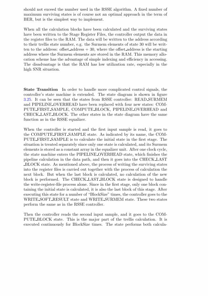
64 Design Specification
should not exceed the number used in the RSSE algorithm. A fixed number ofmaximum surviving states is of course not an optimal approach in the term ofBER, but is the simplest way to implement.
When all the calculation blocks have been calculated and the surviving stateshave been written to the Stage Register Files, the controller output the data inthe register files to the RAM. The data will be written to the address accordingto their trellis state number, e.g. the Surmem elements of state 30 will be writ-ten to the address: offset address + 30, where the offset address is the startingaddress where the Surmem elements are stored in the RAM. This memory allo-cation scheme has the advantage of simple indexing and efficiency in accessing.The disadvantage is that the RAM has low utilization rate, especially in thehigh SNR situation.
State Transition In order to handle more complicated control signals, thecontroller’s state machine is extended. The state diagram is shown in figure3.25. It can be seen that the states from RSSE controller: READ SURMEMand PIPELINE OVERHEAD have been replaced with four new states: COM-PUTE FIRST SAMPLE, COMPUTE BLOCK, PIPELINE OVERHEAD andCHECK LAST BLOCK. The other states in the state diagram have the samefunction as in the RSSE equalizer.
When the controller is started and the first input sample is read, it goes tothe COMPUTE FIRST SAMPLE state. As indicated by its name, the COM-PUTE FIRST SAMPLE is to calculate the initial state in the first stage. Thesituation is treated separately since only one state is calculated, and its Surmemelements is stored as a constant array in the equalizer unit. After one clock cycle,the state machine enters the PIPELINE OVERHEAD state, which finishes thepipeline calculation in the data path, and then it goes into the CHECK LASTBLOCK state. As mentioned above, the process of writing the surviving states
into the register files is carried out together with the process of calculation thenext block. But when the last block is calculated, no calculation of the newblock is performed. The CHECK LAST BLOCK state is designed to handlethe write-register-file process alone. Since in the first stage, only one block con-taining the initial state is calculated, it is also the last block of this stage. Afterexecuting this state for a number of “BlockSize” times, the controller goes to theWRITE SOFT RESULT state and WRITE SURMEM state. These two statesperform the same as in the RSSE controller.
Then the controller reads the second input sample, and it goes to the COM-PUTE BLOCK state. This is the major part of the trellis calculation. It isexecuted continuously for BlockSize times. The state performs both calcula-
3.5 SD Equalizer core 65
����
���������� ��
�����
���������
��������
��������
����
������
�����
������
������!
�"#
��#
��������!
�"����� �$�
������� �$�
��%����%�& �� ��
������'��� �����
�"���� �(�)
�"������ *�+��
������ �(�)
'���������"�'��� ��
������,�!
�"%����%�& �� ��
�������� *�+��
���
�����
����-'������������������
������������!.
��%����%�& �� ��
�����"'��� �����
������
��������
�������
/���
�����
������� �$�
��#
������,�!
�"����� �$�
�"0
��0
������ �(�)
Figure 3.25: State diagram of the SD I equalizer
tion for the new block, and storage of surviving states of the last block intoStage Register Files. After being executed for BlockSize times, it enters thePIPELINE OVERHEAD state. After the PIPELINE OVERHEAD state is fin-ished, the controller will go back to the COMPUTE BLOCK state to calculatethe next block, if there are more blocks in the trellis structure, or go to theCHECK LAST BLOCK state.
3.5.1.4 Timing analysis
Like the RSSE controller, the computation time to process a burst by SD Icontroller is examined. The pipeline structure of the controller is not as efficientas in the RSSE controller. Each state in RSSE takes one clock cycle, and eachsample is calculated in TotalState + PipelineStage - 1 + BlockSize clock cycles.The SD I controller will not start calculation for a new block until the previousblock is totally finished (including the pipeline overhead part). Therefore, ittakes BlockSize + PipelineStage -1 clock cycles to calculate a block, (BlockSize

66 Design Specification
�������� ��������� ������
�������������� ������ �������� ��������� ������
�������������� ������ �������� ��������� ������
������
������
������
���������������������
�����
����� ����
���
���
���������������������
�����
���������������������
�����
���������������������
�����
���������������������
������
�������������������������
������������ �����
�������������������������
������������ �����
����� ���������
�������������� �����������������
��������� ��������
�������������� �����������������
�������������� ������
��������
Figure 3.26: Pipelining the process of the SD I controller
+ PipelineStage -1)*BlockNum + BlockSize clock cycles to finish a stage, asshown in figure 3.26. The computation time of a 32QAM normal symbol rateburst will be
3 + [4 + (32 + 5) ∗ 32 + 32 + 5 + (64 + 2)] ∗ 143 = 184616cc
When using the clock with the maximum frequency = 200MHz, the clock periodis 5ns, and the computation time is
184616 ∗ (5 ∗ 10−9) = 923µs > required 577/2 µs
The 32QAM burst will have too long computation time which cannot hold thetiming requirements. The computation time for the high rate 16QAM burstis 365µs, which holds the timing requirements. The other smaller alphabetmodulation types also hold the timing requirements.
This timing analysis shows that the SD I equalizer cannot be used for equalizingthe 32QAM bursts within the required time. Only the modulation types with
3.5 SD Equalizer core 67
less complexity can be used. However, this approach has the advantage ofpower and area efficiency, therefore it is still implemented in the project. Itsperformance has also been evaluated.
3.5.2 SD II equalizer design
3.5.2.1 SD II Controller unit
This section introduces an alternative approach to implement the SD equalizer,which is referred to as the SD II equalizer. The SD II equalizer differs with theSD I equalizer in its controller unit. The rest part are the same. Therefore onlythe controller design is described here.
The timing analysis shows that the SD I approach failed to hold the timingrequirement of processing a burst in 585 ms. The problem of the SD I approachis that the controller checks one entry of the surviving state list at each clockedge, and decides if this state need to be calculated. Also on the storage side, ittakes 1 clock cycle to check if the new state survives. Since in the SD algorithm,the surviving rate is normally under 25%, which means the controller spends75% of the time checking pruned states. This makes the SD I approach veryinefficient. If the controller can skip all the pruned state and jump directly tothe next surviving state at each clock edge, the computation time to process aburst will be decreased significantly. It requires the controller to be able to:
• implement the efficient search mechanism, so that the time spent on eachstage is approximately equal to the number of surviving states.
• ensure the next block is not started until the previous block is finished withcalculation, since the Block Registers are shared. This is important be-cause the time spent in each block are different, depending on the numberof the surviving states in the block.
The first task is actually to find the index of the first non-zero element inthe array in a efficient way. For example, if the surviving state list [7:0] of an8PSK sample is [1,0,0,1,1,0,1,0], the SD I controller decodes the array in a waythat: ”state 0 pruned”, ”state 1 survives”, ”state 2 pruned”, ”state 3 survives”,”state 4 survives”, ”state 5 pruned”, ”state 6 pruned”, ”state 7 survives”, eachof which takes one clock cycle. The aim of the SD II controller is to ”leave thepruned states out” and decodes the array such that: ”state 1 survives”, ”state 3survives”, ”state 4 survives”, ”state 7 survives” in four consecutive clock cycles.
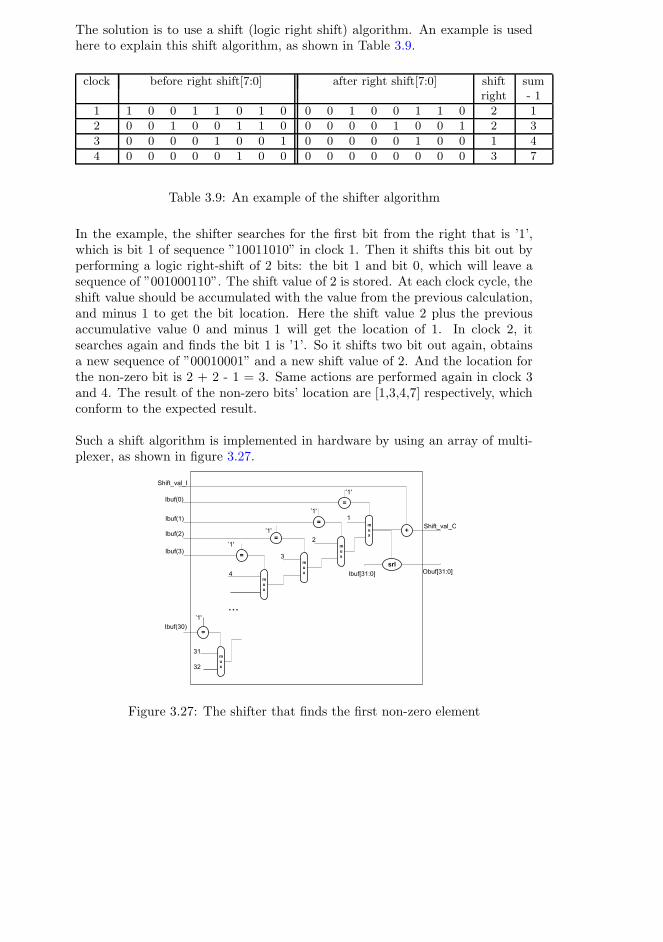
68 Design Specification
The solution is to use a shift (logic right shift) algorithm. An example is usedhere to explain this shift algorithm, as shown in Table 3.9.
clock before right shift[7:0] after right shift[7:0] shift sumright - 1
1 1 0 0 1 1 0 1 0 0 0 1 0 0 1 1 0 2 1
2 0 0 1 0 0 1 1 0 0 0 0 0 1 0 0 1 2 3
3 0 0 0 0 1 0 0 1 0 0 0 0 0 1 0 0 1 4
4 0 0 0 0 0 1 0 0 0 0 0 0 0 0 0 0 3 7
Table 3.9: An example of the shifter algorithm
In the example, the shifter searches for the first bit from the right that is ’1’,which is bit 1 of sequence ”10011010” in clock 1. Then it shifts this bit out byperforming a logic right-shift of 2 bits: the bit 1 and bit 0, which will leave asequence of ”001000110”. The shift value of 2 is stored. At each clock cycle, theshift value should be accumulated with the value from the previous calculation,and minus 1 to get the bit location. Here the shift value 2 plus the previousaccumulative value 0 and minus 1 will get the location of 1. In clock 2, itsearches again and finds the bit 1 is ’1’. So it shifts two bit out again, obtainsa new sequence of ”00010001” and a new shift value of 2. And the location forthe non-zero bit is 2 + 2 - 1 = 3. Same actions are performed again in clock 3and 4. The result of the non-zero bits’ location are [1,3,4,7] respectively, whichconform to the expected result.
Such a shift algorithm is implemented in hardware by using an array of multi-plexer, as shown in figure 3.27.
�
�
�
�
���
�
�����
�� ���������
�
�
�
���
��
�
�
�
���
��
�
�
�
���
������
������
������
�
���
�
�
�
�
������
��
��
�
�� ���������
���
���
��������� ���������
Figure 3.27: The shifter that finds the first non-zero element
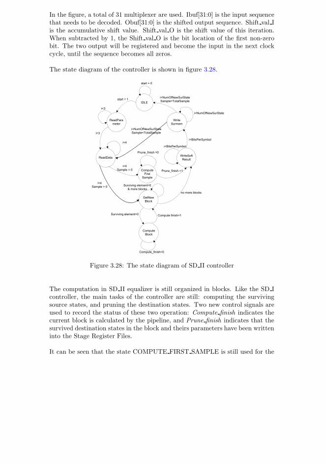
3.5 SD Equalizer core 69
In the figure, a total of 31 multiplexer are used. Ibuf[31:0] is the input sequencethat needs to be decoded. Obuf[31:0] is the shifted output sequence. Shift val Iis the accumulative shift value. Shift val O is the shift value of this iteration.When subtracted by 1, the Shift val O is the bit location of the first non-zerobit. The two output will be registered and become the input in the next clockcycle, until the sequence becomes all zeros.
The state diagram of the controller is shown in figure 3.28.
����
���������� ��
�����
������
�����
��������
����
������
����
�����
�������
�������
��
��
���������
���������!��"��
��#��$�#�% �� ��
������&��� �����
������'��!��"��
�������� (�)��
��*�*�!+������!,�
��#��$�#�% �� ��
�������� (�)��
���
�����
!�������)�����
��#��$�#�% �� ��
������&��� �����
-�#�%
�����
��
������,�� ��*�*�!+������!���
.������)�����
��/
��/
���!�'��!��"���
���!�'��!��"���
Figure 3.28: The state diagram of SD II controller
The computation in SD II equalizer is still organized in blocks. Like the SD Icontroller, the main tasks of the controller are still: computing the survivingsource states, and pruning the destination states. Two new control signals areused to record the status of these two operation: Compute finish indicates thecurrent block is calculated by the pipeline, and Prune finish indicates that thesurvived destination states in the block and theirs parameters have been writteninto the Stage Register Files.
It can be seen that the state COMPUTE FIRST SAMPLE is still used for the
70 Design Specification
first stage of the trellis search. Normally the computing process and the pruningprocess are carried out in parallel. But for the first stage, only one block iscomputed. The block must be computed first, then be pruned. When thePrune finish signal is asserted, the state machine goes to the WRITE SOFTRESULT state, which, same as in the other equalizer controllers, writes the
soft-bit result to the RAM.
From the second stage, after reading the input sample from the RAM, thestate machine goes to a GET NEW BLOCK state. This state checks if there isany surviving source state in the block by comparing the surviving list of thesource states of a block with a value of all 0’s. If all the states in the blockare pruned, the state machine will stay in the current state, and check the nextblock. Otherwise, the state machine goes to the COMPUTE BLOCK state,which handles the computing and pruning processes. Two special situationsmay occur in this state:
• No more new block is left. The controller will only perform pruning oper-ation in the next COMPUTE BLOCK state.
• After the controller finishes pruning operation mentioned above, the con-troller still goes back to the GET NEW BLOCK state. In this case thestate machine will go to the WRITE SOFT RESULT state in the nextclock cycle.
In the COMPUTE BLOCK state, the controller performs both the computationof the new path metric of the current block, and the pruning of the destinationstates of the last block. It decodes both the surviving list of the source states ofthe current block and the surviving list of the next block, by using the shiftershown in figure 3.27. Some more control signals are used for the decoding, whichinclude:
• shift en: This signal is the enable signal of the shifter. This signal is usedto prevent unwanted shift operations.
• index valid: This signal is output by the shifter to indicate the non-zeroindex found by the shifter is valid.
• mem valid: This signal is used to indicate the data from the RAM isvalid. Since there is a 2 clock-cycle delay between the address and data, itis easier to use such a signal to capture the valid data, instead of countingthe clock cycles between the address and data.
• mem valid advanced1: This signal is used to indicate the data from theRAM in the next clock cycle is valid.
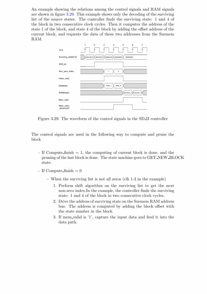
3.5 SD Equalizer core 71
An example showing the relations among the control signals and RAM signalsare shown in figure 3.29. This example shows only the decoding of the survivinglist of the source states. The controller finds the surviving state: 1 and 4 ofthe block in two consecutive clock cycles. Then it computes the address of thestate 1 of the block, and state 4 of the block by adding the offset address of thecurrent block, and requests the data of these two addresses from the SurmemRAM.
�������� �������� �������� ��������
� �
������ ������
����� �����
� �
�������������������
��������
��������������
�������!��
"�#����
"�#$��� �
#����!��
#����!���
�����%���
� & ' � ( ) �
��������
Figure 3.29: The waveform of the control signals in the SD II controller
The control signals are used in the following way to compute and prune theblock
- If Compute finish = 1, the computing of current block is done, and thepruning of the last block is done. The state machine goes to GET NEW BLOCKstate.
- If Compute finish = 0
– When the surviving list is not all zeros (clk 1-3 in the example)
1. Perform shift algorithm on the surviving list to get the nextnon-zero index.In the example, the controller finds the survivingstate: 1 and 4 of the block in two consecutive clock cycles.
2. Drive the address of surviving state on the Surmem RAM addressbus. The address is computed by adding the block offset withthe state number in the block.
3. If mem valid is ’1’, capture the input data and feed it into thedata path.
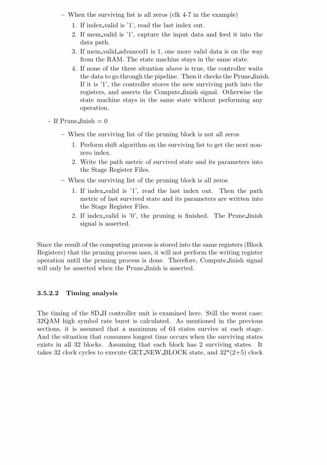
72 Design Specification
– When the surviving list is all zeros (clk 4-7 in the example)
1. If index valid is ’1’, read the last index out.
2. If mem valid is ’1’, capture the input data and feed it into thedata path.
3. If mem valid advanced1 is 1, one more valid data is on the wayfrom the RAM. The state machine stays in the same state.
4. If none of the three situation above is true, the controller waitsthe data to go through the pipeline. Then it checks the Prune finish.If it is ’1’, the controller stores the new surviving path into theregisters, and asserts the Compute finish signal. Otherwise thestate machine stays in the same state without performing anyoperation.
- If Prune finish = 0
– When the surviving list of the pruning block is not all zeros
1. Perform shift algorithm on the surviving list to get the next non-zero index.
2. Write the path metric of survived state and its parameters intothe Stage Register Files.
– When the surviving list of the pruning block is all zeros
1. If index valid is ’1’, read the last index out. Then the pathmetric of last survived state and its parameters are written intothe Stage Register Files.
2. If index valid is ’0’, the pruning is finished. The Prune finishsignal is asserted.
Since the result of the computing process is stored into the same registers (BlockRegisters) that the pruning process uses, it will not perform the writing registeroperation until the pruning process is done. Therefore, Compute finish signalwill only be asserted when the Prune finish is asserted.
3.5.2.2 Timing analysis
The timing of the SD II controller unit is examined here. Still the worst case:32QAM high symbol rate burst is calculated. As mentioned in the previoussections, it is assumed that a maximum of 64 states survive at each stage.And the situation that consumes longest time occurs when the surviving statesexists in all 32 blocks. Assuming that each block has 2 surviving states. Ittakes 32 clock cycles to execute GET NEW BLOCK state, and 32*(2+5) clock

3.6 RSSE T Equalizer core 73
cycles to execute COMPUTE BLOCK state, where 2+5 is the pipeline latencyof processing 2 states. Together, the computation time for process a burst is
3 + [4 + 32 + (2 + 5) ∗ 32 + 5 + (64 + 2)] ∗ 171 = 55604cc
When using the clock with the maximum frequency = 200MHz, the clock periodis 5ns, and the computation time is
55604 ∗ (5 ∗ 10−9) = 283µs < required 577/2µs
The calculation shows that the SD II controller holds the timing requirements.
3.6 RSSE T Equalizer core
3.6.1 Equalizer Design
The RSSE T Equalizer is a hybrid equalizer, which uses the reduced trellisstructure of the RSSE equalizer, and applies the threshold constraint in thepath metric computation. So it is apparent that the RSSE T equalizer shouldhave a data path which is a combination of both RSSE and SD equalizers, shownin figure 3.30. It can be seen that most of the data path in SD equalizer arekept. Only the 32-input equalizer is replaced by the Parallel comparator and8-input comparator. And the Merge path unit are changed back to the one usedin the RSSE equalizer. The controller unit of the RSSE T equalizer should bevery similar to the one in the SD equalizer. A decision should be made beforeimplementing the controller: is the SD I controller or the SD II controller amore suitable approach in this hybrid design?
From the description of the two SD equalizers, it can be seen that the SD Iequalizer is straightforward in implementation. The controller unit is muchsimpler than the SD II equalizer. The disadvantage is that it takes too longtime to calculate a trellis structure with many states. Since the RSSE trellisstructure has significantly reduced states compared to the full trellis structure,the computation time problem in SD I equalizer will not occur to the RSSE Tequalizer. Therefore the SD I approach is selected.
The controller design has the same state diagram as for the SD I controller.Minor modifications are applied on the SD I controller:
• Pipeline stages are changed from 6 to 7, thus the controller signals prop-agated by the pipeline registers should be modified.
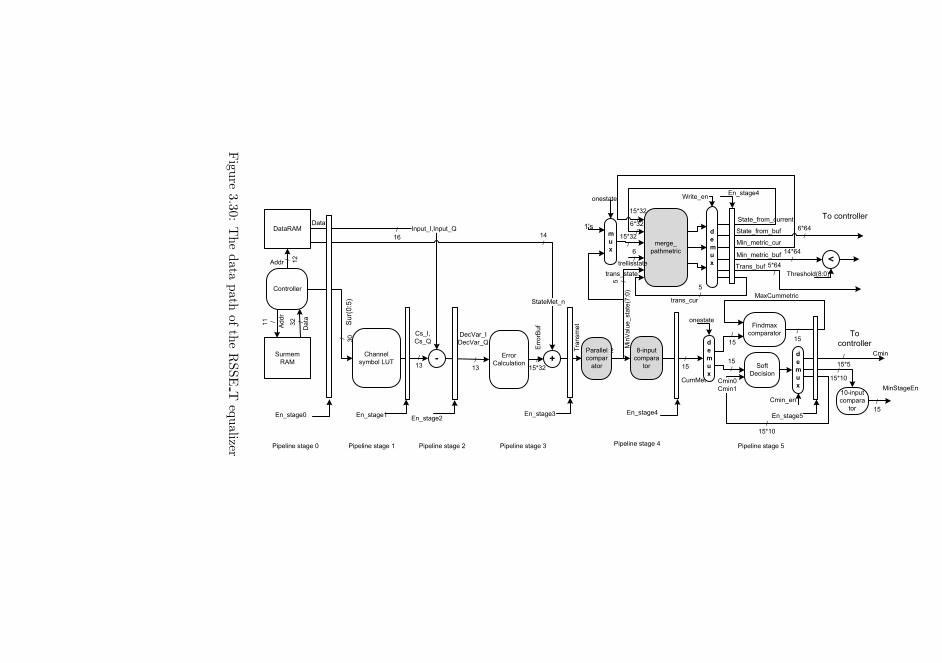
74
Desig
nS
pecifi
catio
n
�������
�������
� ����
���������� �
�������������
���
����������
�������
�������
�
��������
������
��!��
��� �����
�"��
�������
��#�"
�����������
�����"�����"
�
�
�
�
����$
���%
���
�������
�
�
�
�
�
�����"�������
������"
�����������"
&
%'&
%'
�($)*+
�����
����
������
�����
, �����
�����������
-����������!��% -����������!��. -����������!��' -����������!��/ -����������!��*
����������
��� ����
���
-����������!��$
�
�
�
%0�
�
�
�
�
�
1�2��3
��������
�������
�������
�����!�$ �����!�%�����!�.
�����!�' �����!�/
�����!�/
�����!�*
�22
����
�22
����
& %.
%% &
&
%4
'. &
& '$
&
%*5'.
%/
&
&
%*
%*5'.
&
%*5'.
&
%*5'.
&
4
&
45'.
&
&
%*
%*
&
&
%*
&
%*5%$
&
%*5*
��3��������
%/54/
&
454/
&
*54/
&
�
� �� ��2(6)$+
%$7����
������
��
&
%*5%$
�� ��!��
&
%*
-�������
�����
���
67�����
������
��
���������
�������������(8)$+
������
*
&
* &
Fig
ure
3.3
0:
Th
ed
ata
path
of
the
RS
SE
Teq
ualizer

3.6 RSSE T Equalizer core 75
• Some signals have different length, e.g. the Trellis state signal indicatingthe which state the controller is calculating is 10 bits in SD controller, andis 6 bits in RSSE T controller.
3.6.2 Timing Analysis
Since the RSSE T equalizer uses the SD I approach, it is expected that it takesa little longer time than the RSSE equalizer, due to the overhead in block cal-culation. The time needed for processing a high symbol rate 32QAM burstis: 3 + [4 + (BlockSize + PipelineStage − 1) ∗ TotalBlock + BlockSize +BitsperSymbol+ TotalState+ 2] ∗ TotalSample
= 3 + [4 + (8 + 6) ∗ 8 + 8 + 5 + (64 + 2)] ∗ 171 = 33348cc
When using the clock with the maximum frequency at 200MHz, the clock periodis 5ns, and the computation time is
33348 ∗ (5 ∗ 10−9) = 167µs < required 577/2 µs
For the RSSE T equalizer, the worse case is the 64 state 8PSK burst, since ithas 16 blocks in one stage. The computation time is 34180 clock cycles, whichstill holds the timing constraints when using 200MHz clock.

76 Design Specification
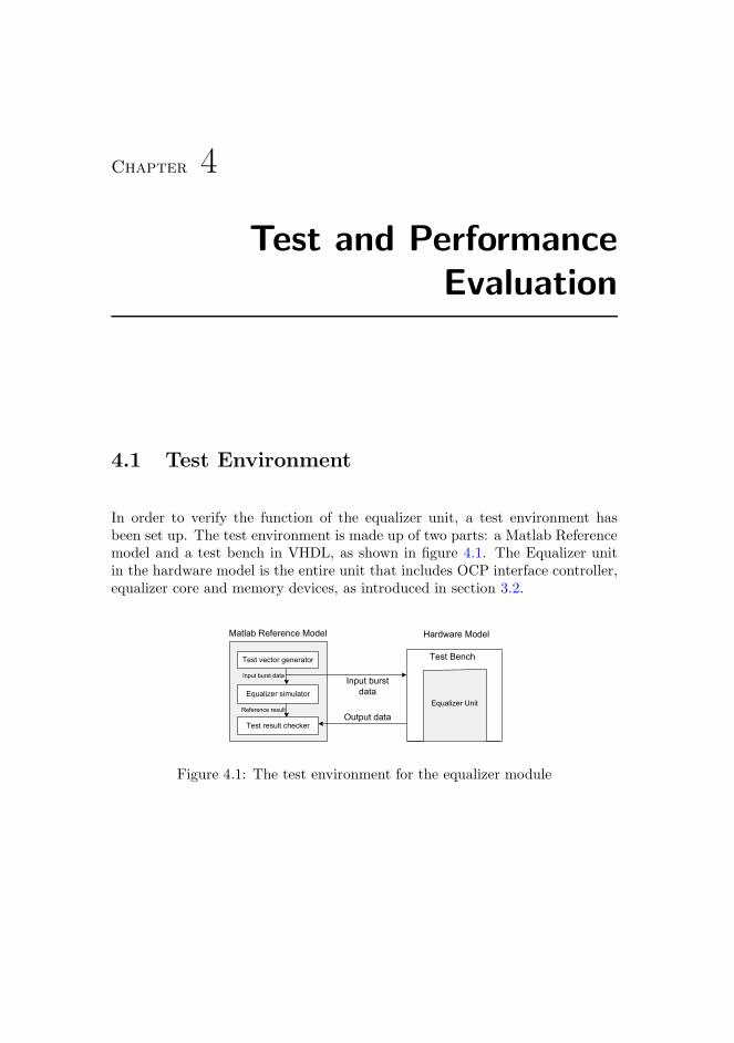
Chapter 4
Test and PerformanceEvaluation
4.1 Test Environment
In order to verify the function of the equalizer unit, a test environment hasbeen set up. The test environment is made up of two parts: a Matlab Referencemodel and a test bench in VHDL, as shown in figure 4.1. The Equalizer unitin the hardware model is the entire unit that includes OCP interface controller,equalizer core and memory devices, as introduced in section 3.2.
�����������
���� ���
�� �
�� �� �� �
�� ����������������
��� ��� ������ �
�������������� �
��� ���� ������
������������
���� ��� �� �
��� �������
��� !����
Figure 4.1: The test environment for the equalizer module
78 Test and Performance Evaluation
The Matlab Reference Model
As shown in the figure, the Matlab reference model has been implemented asa Test vector generator, an Equalizer simulator which simulates the behaviorof the equalizer, and a Test result checker which compares the output soft-bitresult from the hardware model with the reference result from the Equalizersimulator.
The Test vector generator can generates a burst of any required modulationtype. The burst is formed by the correspondent tail bits of the modulationtype, followed by an array of random data added with noise of a specified noiserange. The burst data is saved as an input.dat file, which will be read by boththe Equalizer simulator and the hardware model.
A separate Equalizer simulator is implemented for each of the algorithm imple-mented in the hardware model: RSSE, SD and RSSE T. The equalizer simula-tor can be configured into processing any of the required modulation type data.Besides, a one-state equalizer simulator is also implemented to calculate thethreshold used by the SD and RSSE T equalizer simulators. The equalizer sim-ulators function exactly the same as the corresponding hardware models. Whenthey read the test burst data generated by the Test vector generator, they pro-duce the reference soft-bit results. The results are stored into a ref out.dat file,and will be used by the Test result checker.
The input burst data is also read by the test bench in the hardware model. Thehardware model performs equalizing on the input data, and stores the soft-bitresults in an output.dat file. This file is also used by the Test result checker.The test bench will be described in details in the next section.
The Test result checker compares the data of the ref out.dat and the data ofthe output.dat file. If all the value are equal, the hardware model functions thesame as the reference model, which is the expected outcome of the test.
Test bench of the Hardware Model
The test bench is implemented to verify the function of the equalizer. Besides,the test bench is also used for power evaluation of the design. When the systemis powered up, it configures the equalizer unit according to the modulation typeof the current burst, streams in the data from the input.dat, and sends it to theRAM of the equalizer unit via OCP interface. Then it waits until the equalizerfinishes processing the burst, and asserts the interrupt signal. The test bench

4.2 Functional test 79
then fetches data from the RAM of the equalizer, and saves the data into theoutput.dat.
4.2 Functional test
The functional test has been carried out for all 4 hardware implementation ofthe equalizers. The test cases cover all the required modulation types in twopossible symbol rate. The test is made on both the RTL model and the gatelevel model with no annotated delay. The clock frequency is set at 200MHz. Alist of the test cases are shown below in the table 4.1.
Not all the test case can be applied on all the equalizers. The test cases thatdo not match the algorithm of the equalizer are crossed out in the table. The32QAM 1024 state case takes too long time for the SD I equalizer to performequalizing, which is known before the implementation. Other feasible test casespresented the correct results.
case Modulation Total Total RSSE SD I SD II RSSE Ttype State Sample result result result result
1 GMSK 16 143 correct correct correct correct
2 GMSK 32 143 correct correct correct correct
3 QPSK 64 171 correct correct correct correct
4 8PSK 16 143 correct - - correct
5 8PSK 64 143 correct correct correct correct
6 16QAM 64 143 correct - - correct
7 16QAM 64 171 correct - - correct
8 16QAM 256 143 - correct correct -
9 16QAM 256 171 - correct correct -
10 32QAM 64 143 correct - - correct
11 32QAM 64 171 correct - - correct
12 32QAM 1024 143 - violate timing correct -
13 32QAM 1024 171 - violate timing correct -
Table 4.1: The test cases and the results
4.3 Timing analysis
The timing of the design is checked by Synopsys’s report timing function. Beforesynthesizing the design with the Synopsys DC, a timing constraint of clock cycle
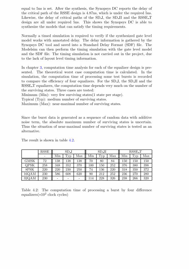
80 Test and Performance Evaluation
equal to 5ns is set. After the synthesis, the Synopsys DC reports the delay ofthe critical path of the RSSE design is 4.87ns, which is under the required 5ns.Likewise, the delay of critical paths of the SD I, the SD II and the RSSE Tdesign are all under required 5ns. This shows the Synopsys DC is able tosynthesize the models that can satisfy the timing requirements.
Normally a timed simulation is required to verify if the synthesized gate levelmodel works with annotated delay. The delay information is gathered by theSynopsys DC tool and saved into a Standard Delay Format (SDF) file. TheModelsim can then perform the timing simulation with the gate level modeland the SDF file. The timing simulation is not carried out in the project, dueto the lack of layout level timing information.
In chapter 3, computation time analysis for each of the equalizer design is pre-sented. The theoretical worst case computation time is calculated. In thesimulation, the computation time of processing some test bursts is recordedto compare the efficiency of four equalizers. For the SD I, the SD II and theRSSE T equalizers, the computation time depends very much on the number ofthe surviving states. Three cases are tested:Minimum (Min): very few surviving states(1 state per stage).Typical (Typ): medium number of surviving states.Maximum (Max): near-maximal number of surviving states.
Since the burst data is generated as a sequence of random data with additivenoise term, the absolute maximum number of surviving states is uncertain.Thus the situation of near-maximal number of surviving states is tested as analternative.
The result is shown in table 4.2.
RSSE SD I SD II RSSE T- Min Typ Max Min Typ Max Min Typ Max
GMSK 72 138 138 138 70 80 84 150 150 150
QPSK 258 348 352 370 100 150 252 376 380 398
8PSK 220 220 230 250 74 136 220 318 350 372
16QAM 230 586 608 620 90 212 252 236 270 280
32QAM 230 - - - 114 228 326 238 266 320
Table 4.2: The computation time of processing a burst by four differenceequalizers(∗102 clock cycles)

4.4 Area analysis 81
4.4 Area analysis
The area of the equalizer design is examined by the report area function of theSynopsys DC. As the equalizer core is the most interesting part to examine,the area measurements are made only on the equalizer core. The measurementbelow doesn’t include the OCP interface controller or the memory device. Thearea cost of the equalizer core of four different algorithms is shown in table 4.3.It is evident that AreaRSSE < AreaRSSE T < AreaSD I < AreaSD II . Thearea of the SD II equalizer is twice as much as the SD I equalizer, and almostthree times as much as the area of the RSSE equalizer.
The area of the sub-modules in the equalizer core are shown in table 4.4 and4.5. The controller unit in the equalizer core is the biggest part in the equalizerdesign, most of which is contributed by the register files, as discussed in 3.4.4.7.The Error Calculation module which contains ten multipliers also contributesmuch to the total area cost.
Overall, RSSE and RSSE T equalizers have lower area cost than the others.
RSSE SD I SD II RSSE T
Nets 13726 25374 56790 19758
Cells 10056 18321 45522 13902
Combinational 35902 49416 110678 42383
Non-Combinational 26199 44634 72287 35933
Total Cell Area 62102 94050 182965 78317
Table 4.3: The area cost for the four equalizers of different algorithms
RSSE RSSE Tarea(µm2) % area(µm2) %
Equalizer 62102 100 78317 100
ChannelSymbol LUT 2518 4.1 2542 3.2
Error Calculation 10703 17.2 10275 13
Merge Path 971 1.6 970 1.2
Soft Decision 1001 1.6 1001 1.3
Parallel Compare 4760 7.7 4756 6
8-input Compare 666 1.1 743 0.9
10-input Compare - - 1060 1.4
Controller unit 41422 66.7 57172 73
Table 4.4: The area cost of each module of the RSSE and the RSSE T equalizers.
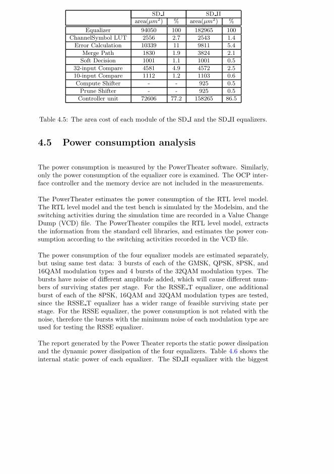
82 Test and Performance Evaluation
SD I SD IIarea(µm2) % area(µm2) %
Equalizer 94050 100 182965 100
ChannelSymbol LUT 2556 2.7 2543 1.4
Error Calculation 10339 11 9811 5.4
Merge Path 1830 1.9 3824 2.1
Soft Decision 1001 1.1 1001 0.5
32-input Compare 4581 4.9 4572 2.5
10-input Compare 1112 1.2 1103 0.6
Compute Shifter - - 925 0.5
Prune Shifter - - 925 0.5
Controller unit 72606 77.2 158265 86.5
Table 4.5: The area cost of each module of the SD I and the SD II equalizers.
4.5 Power consumption analysis
The power consumption is measured by the PowerTheater software. Similarly,only the power consumption of the equalizer core is examined. The OCP inter-face controller and the memory device are not included in the measurements.
The PowerTheater estimates the power consumption of the RTL level model.The RTL level model and the test bench is simulated by the Modelsim, and theswitching activities during the simulation time are recorded in a Value ChangeDump (VCD) file. The PowerTheater compiles the RTL level model, extractsthe information from the standard cell libraries, and estimates the power con-sumption according to the switching activities recorded in the VCD file.
The power consumption of the four equalizer models are estimated separately,but using same test data: 3 bursts of each of the GMSK, QPSK, 8PSK, and16QAM modulation types and 4 bursts of the 32QAM modulation types. Thebursts have noise of different amplitude added, which will cause different num-bers of surviving states per stage. For the RSSE T equalizer, one additionalburst of each of the 8PSK, 16QAM and 32QAM modulation types are tested,since the RSSE T equalizer has a wider range of feasible surviving state perstage. For the RSSE equalizer, the power consumption is not related with thenoise, therefore the bursts with the minimum noise of each modulation type areused for testing the RSSE equalizer.
The report generated by the Power Theater reports the static power dissipationand the dynamic power dissipation of the four equalizers. Table 4.6 shows theinternal static power of each equalizer. The SD II equalizer with the biggest

4.5 Power consumption analysis 83
area cost has also the biggest internal static power dissipation, and the RSSEequalizer has the smallest static power dissipation.
Pstatic(µW )
RSSE 49
SD I 50
SD II 114
RSSE T 59
Table 4.6: The static power dissipation of the four equalizers(µW )
The dynamic power dissipation of the RSSE equalizer is shown in table 4.7.From the table, it is seen that the 32QAM burst consumes the most power.This is the same as expected, as the 32QAM is the modulation type of thelargest alphabet the equalizer can handle, and it uses all the computationalresource. For the bursts of smaller alphabet modulation types, not all theregisters and logics are used. For example the Error Calculation module willuse all the 32 output registers for the 32QAM burst, while only 16 of themare used for the 16QAM burst. Therefore the power dissipation of the smalleralphabet modulation types is less than that of the larger alphabet modulationtypes. The QPSK 64-state consumes more power than the 16QAM and 8PSK,because the QPSK has a 20% more samples in the burst. Therefore the payloadvs. overhead is bigger than those two modulation types.
Pdynamic(mW )
GMSK 16-state 7.02
GMSK 32-state 7.3
QPSK 64-state 8.15
8PSK 16-state 7.63
8PSK 64-state 7.88
16QAM 64-state 7.85
32QAM 64-state 8.19
Table 4.7: The dynamic power consumption of processing a burst by RSSEequalizers(mW)
The dynamic power dissipation of the SD I and the SD II equalizers is shownin table 4.8 and 4.9, respectively. The results are presented as dynamic powerdissipation versus the average number of surviving states per stage. In bothequalizers, the 8PSK consumes more power than the larger alphabet modulationtypes. It is because in the full trellis structure, the 8PSK has much smaller

84 Test and Performance Evaluation
number of total states (64) than 16QAM (256) and 32QAM (1024). For the samelevel of average surviving states, the surviving states distribute more closely in8PSK trellis structure, and therefore the data path are enabled more frequentlywhen processing 8PSK burst than 16QAM and 32QAM burst.
The results in table 4.8 and 4.9 are plotted in the figure 4.2. From the figures, itcan be seen that the SD I equalizer consumes less power than the SD II equalizerin general.
Pdynamic(mW) / Surv. State Per Stage
GMSK 16-state 4.36 / 1 4.69 / 2 4.84 / 3
QPSK 64-state 4.07 / 1 4.77 / 4 5.73 / 13
8PSK 64-state 5.12 / 1 5.71 / 8 6.83 / 23
16QAM 256-state 3.48 / 1 5.07 / 17 5.43 / 25
Table 4.8: The dynamic power consumption of processing a burst by SD I equal-izers(mW)
Pdynamic (mW) / Surv. State Per Stage
GMSK 16-state 6.6 / 1 7.1 / 2 7.3 / 3 -
QPSK 64-state 7.52 / 1 8.42 / 4 9.48 / 13 -
8PSK 64-state 7.9 / 1 9.51/ 8 10.3 / 23 -
16QAM 256-state 7.5 / 1 9.7 / 17 10 / 25 -
32QAM 1024-state 7.2 / 1 9.15 / 14 9.5 / 20 9.9 / 33
Table 4.9: The dynamic power consumption of processing a burst by SD IIequalizers(mW)
0510152025303
4
5
6
7
8
9
10
11
Average surviving states per stage
Pow
er c
onsu
mpt
ion
(mW
)
Power consumption of the SD_I algorithm
16QAM8PSKQPSKGMSK
051015202530353
4
5
6
7
8
9
10
11
Average surviving states per stage
Pow
er c
onsu
mpt
ion
(mW
)
Power consumption of the SD_II algorithm
32QAM
16QAM
8PSK
QPSK
GMSK
Figure 4.2: The dynamic power consumption of SD I and SD II equalizer whenprocessing different types of burst
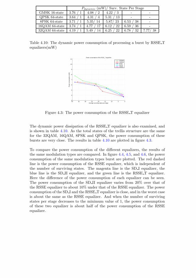
4.5 Power consumption analysis 85
Pdynamic (mW)/ Surv. State Per Stage
GMSK 16-state 3.76 / 1 4.08 / 2 4.22 / 3 - -
QPSK 64-state 3.64 / 1 4.31 / 4 5.31 / 13 - -
8PSK 64-state 3.71 / 1 5.35/ 14 5.87/ 23 6.53 / 38 -
16QAM 64-state 3.74 / 1 4.77 / 17 6.12 / 22 6.59 / 36 -
32QAM 64-state 4.19 / 1 5.49 / 14 6.25 / 22 6.78 / 32 7.77/ 38
Table 4.10: The dynamic power consumption of processing a burst by RSSE Tequalizers(mW)
05101520253035403
4
5
6
7
8
9
10
11Power consumption of the RSSE_T algorithm
Average surviving states per stage
Pow
er c
onsu
mpt
ion
(mW
)
32QAM16QAM8PSKQPSKGMSK
Figure 4.3: The power consumption of the RSSE T equalizer
The dynamic power dissipation of the RSSE T equalizer is also examined, andis shown in table 4.10. As the total states of the trellis structure are the samefor the 32QAM, 16QAM, 8PSK and QPSK, the power consumption of thesebursts are very close. The results in table 4.10 are plotted in figure 4.3.
To compare the power consumption of the different equalizers, the results ofthe same modulation types are compared. In figure 4.4, 4.5, and 4.6, the powerconsumption of the same modulation types burst are plotted. The red dashedline is the power consumption of the RSSE equalizer, which is independent ofthe number of surviving states. The magenta line is the SD I equalizer, theblue line is the SD II equalizer, and the green line is the RSSE T equalizer.Here the difference of the power consumption of each equalizer can be seen.The power consumption of the SD II equalizer varies from 20% over that ofthe RSSE equalizer to about 10% under that of the RSSE equalizer. The powerconsumption of the SD I and the RSSE T equalizer is close, and in the worst caseis about the same as the RSSE equalizer. And when the number of survivingstates per stage decreases to the minimum value of 1, the power consumptionof these two equalizer is about half of the power consumption of the RSSEequalizer.
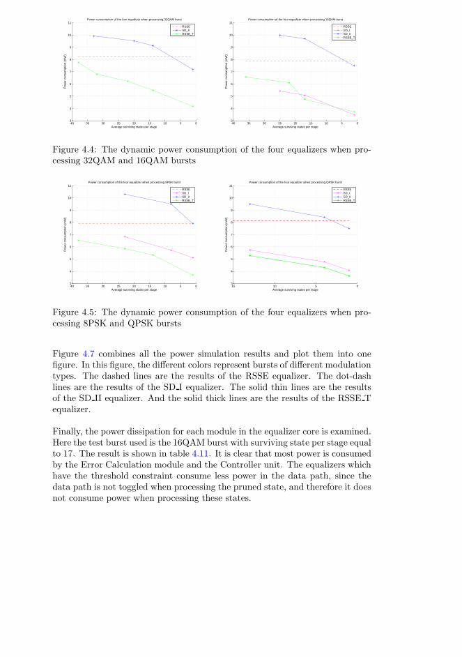
86 Test and Performance Evaluation
05101520253035403
4
5
6
7
8
9
10
11
Average surviving states per stage
Pow
er c
onsu
mpt
ion
(mW
)
Power consumption of the four equalizer when processing 32QAM burst
RSSESD_IIRSSE_T
05101520253035403
4
5
6
7
8
9
10
11
Average surviving states per stage
Pow
er c
onsu
mpt
ion
(mW
)
Power consumption of the four equalizer when processing 16QAM burst
RSSESD_ISD_IIRSSE_T
Figure 4.4: The dynamic power consumption of the four equalizers when pro-cessing 32QAM and 16QAM bursts
05101520253035403
4
5
6
7
8
9
10
11
Average surviving states per stage
Pow
er c
onsu
mpt
ion
(mW
)
Power consumption of the four equalizer when processing 8PSK burst
RSSESD_ISD_IIRSSE_T
0510153
4
5
6
7
8
9
10
11
Average surviving states per stage
Pow
er c
onsu
mpt
ion
(mW
)
Power consumption of the four equalizer when processing QPSK burst
RSSESD_ISD_IIRSSE_T
Figure 4.5: The dynamic power consumption of the four equalizers when pro-cessing 8PSK and QPSK bursts
Figure 4.7 combines all the power simulation results and plot them into onefigure. In this figure, the different colors represent bursts of different modulationtypes. The dashed lines are the results of the RSSE equalizer. The dot-dashlines are the results of the SD I equalizer. The solid thin lines are the resultsof the SD II equalizer. And the solid thick lines are the results of the RSSE Tequalizer.
Finally, the power dissipation for each module in the equalizer core is examined.Here the test burst used is the 16QAM burst with surviving state per stage equalto 17. The result is shown in table 4.11. It is clear that most power is consumedby the Error Calculation module and the Controller unit. The equalizers whichhave the threshold constraint consume less power in the data path, since thedata path is not toggled when processing the pruned state, and therefore it doesnot consume power when processing these states.
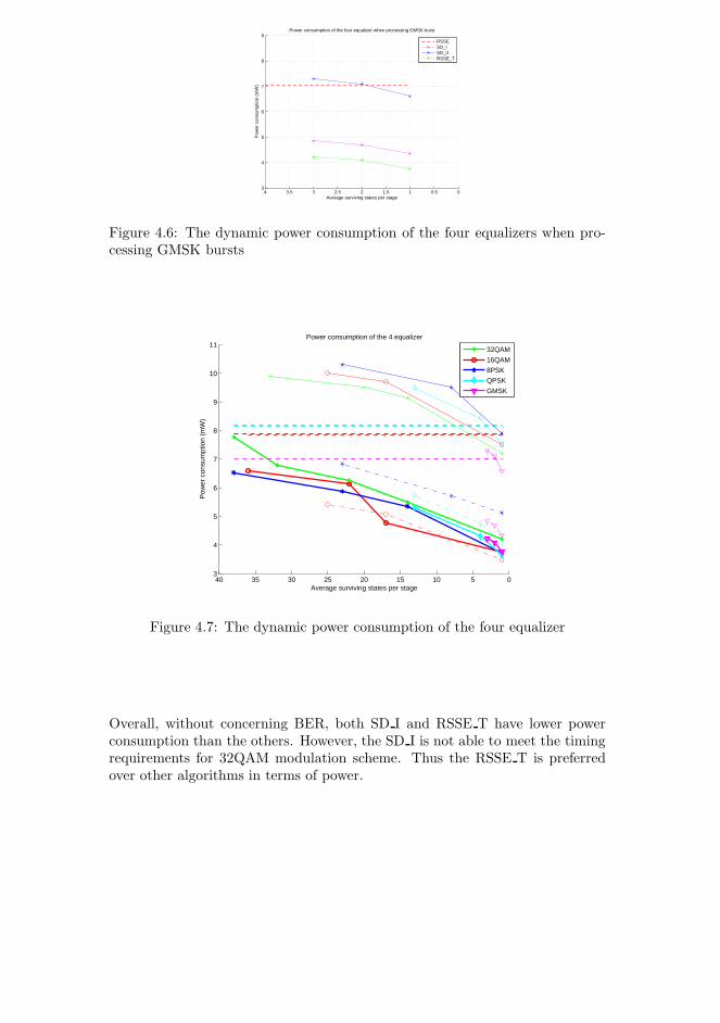
4.5 Power consumption analysis 87
00.511.522.533.543
4
5
6
7
8
9
Average surviving states per stage
Pow
er c
onsu
mpt
ion
(mW
)
Power consumption of the four equalizer when processing GMSK burst
RSSESD_ISD_IIRSSE_T
Figure 4.6: The dynamic power consumption of the four equalizers when pro-cessing GMSK bursts
05101520253035403
4
5
6
7
8
9
10
11Power consumption of the 4 equalizer
Average surviving states per stage
Pow
er c
onsu
mpt
ion
(mW
)
32QAM
16QAM
8PSK
QPSK
GMSK
Figure 4.7: The dynamic power consumption of the four equalizer
Overall, without concerning BER, both SD I and RSSE T have lower powerconsumption than the others. However, the SD I is not able to meet the timingrequirements for 32QAM modulation scheme. Thus the RSSE T is preferredover other algorithms in terms of power.

88 Test and Performance Evaluation
Pdyn RSSE Pdyn SD I 17 Pdyn SD II 17 Pdyn RSSE T 17
(µW ) (µW ) (µW ) (µW )
Equalizer 7850 5070 9700 4770
ChannelSymbol LUT 101 99.6 89.9 97.7
Error Calculation 3950 2010 2860 2170
Merge Path 32.8 45.3 91.9 8.68
Soft Decision 66 5.46 18 4.51
Parallel Compare 426 - - 275
8-input Compare 35.9 - - 1.68
32-input Compare - 85.9 225 -
10-input Compare - 2.44 0.869 0.629
Compute Shifter - - 26.8 -
Prune Shifter - - 23.6 -
Controller unit 3238.3 2821.3 6363.9 2211.8
Table 4.11: The dynamic power dissipation of each module(µW ), in 16QAMmodulation type, with average surviving states of 17 in each stage
4.6 Energy consumption analysis
For mobile devices, the energy consumption is a crucial performance factor. Theenergy consumption is generally the sum of the power dissipation over time. Theenergy for processing a TDMA frame can be described as:
E = Pdynamic ∗ tcomputation + Pstatic ∗ tidle (4.1)
Where E represents energy in Joule, P represents power in Watt, and t representstime in Second.
Two cases of energy consumption are calculated for evaluating the algorithms.The first case assumes that only one slot of a eight-slot frame carries data burst.The second case assumes that five slots in a frame carry data burst. In the firstcase, the computation time is only about 1/16 of the entire frame, since theburst is normally transmitted within 1/2 slot time, while the computation timein the second case is about 5/16 of the entire frame. Therefore the static powercan have a relatively bigger contribution for the total energy consumption inthe first case than in the second case.
As in the computation time measurement, three different levels of survivingstates are calculated for the SD I, the SD II and the RSSE T equalizers:Minimum (Min): very few surviving states(1 state per stage).Typical (Typ): medium number of surviving states.Maximum (Max): near-maximal number of surviving states.

4.6 Energy consumption analysis 89
The calculated results of 1 slot per frame are shown in table 4.12 and figure 4.8.The calculated results of 5 slots per frame are shown in table 4.13 and figure4.9.
ERSSE ESD I(µJ) ESD II (µJ) ERSSE T (µJ)(µJ) Min Typ Max Min Typ Max Min Typ Max
GMSK 0.47 0.52 0.55 0.56 0.75 0.81 0.83 0.53 0.56 0.57
QPSK 1.27 0.93 1.06 1.28 0.89 1.15 1.71 0.93 1.07 1.30
8PSK 1.08 0.78 0.88 1.08 0.81 1.16 1.65 0.84 1.27 1.46
16QAM 1.12 1.23 1.76 1.90 0.85 1.54 1.77 0.69 1.07 1.17
32QAM 1.16 - - - 0.93 1.56 2.12 0.75 1.08 1.49
Table 4.12: The energy consumption of processing 1 TDMA frame by fourdifferent equalizers(µJ), with duty cycle of 1 slot per frame
05101520253035400.4
0.6
0.8
1
1.2
1.4
1.6
1.8
2
2.2
Average surviving states per stage
Ene
rgy
cons
umpt
ion
(µJ)
Energy consumption of a TDMA frame, with duty cycle of 1 slot per frame, using the RSSE equalizer
32QAM16QAM8PSKQPSKGMSK
05101520253035400.4
0.6
0.8
1
1.2
1.4
1.6
1.8
2
2.2
Average surviving states per stage
Ene
rgy
cons
umpt
ion
(µJ)
Energy consumption of a TDMA frame, with duty cycle of 1 slot per frame, using the RSSE_T equalizer
32QAM16QAM8PSKQPSKGMSK
05101520253035400.4
0.6
0.8
1
1.2
1.4
1.6
1.8
2
2.2
Average surviving states per stage
Ene
rgy
cons
umpt
ion
(µJ)
Energy consumption of a TDMA frame, with duty cycle of 1 slot per frame, using the SD_I equalizer
16QAM8PSKQPSKGMSK
05101520253035400.4
0.6
0.8
1
1.2
1.4
1.6
1.8
2
2.2
Average surviving states per stage
Ene
rgy
cons
umpt
ion
(µJ)
Energy consumption of a TDMA frame, with duty cycle of 1 slot per frame, using the SD_II equalizer
32QAM16QAM8PSKQPSKGMSK
Figure 4.8: The energy consumption of processing 1 TDMA frame by fourequalizers, with duty cycle of 1 slot per frame. Top left: RSSE. Top right:RSSE T. Bottom left: SD I. Bottom right: SD II.
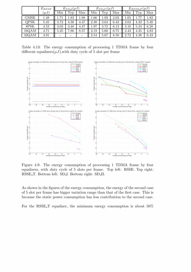
90 Test and Performance Evaluation
ERSSE ESD I(µJ) ESD II (µJ) ERSSE T (µJ)(µJ) Min Typ Max Min Typ Max Min Typ Max
GMSK 1.48 1.71 1.83 1.88 1.66 1.92 2.03 1.65 1.77 1.82
QPSK 5.45 3.72 4.38 4.47 2.38 3.64 6.43 3.63 4.32 5.48
8PSK 4.53 3.02 3.48 4.47 1.97 3.72 6.13 3.16 5.34 6.28
16QAM 4.71 5.25 7.86 8.57 2.19 5.60 6.75 2.43 4.35 4.83
32QAM 4.91 - - - 2.54 5.67 8.50 2.72 4.38 6.43
Table 4.13: The energy consumption of processing 1 TDMA frame by fourdifferent equalizers(µJ),with duty cycle of 5 slot per frame
05101520253035401
2
3
4
5
6
7
8
9
Average surviving states per stage
Ene
rgy
cons
umpt
ion
(µJ)
Energy consumption of a TDMA frame, with duty cycle of 5 slot per frame, using the RSSE equalizer
32QAM16QAM8PSKQPSKGMSK
05101520253035401
2
3
4
5
6
7
8
9
Average surviving states per stage
Ene
rgy
cons
umpt
ion
(µJ)
Energy consumption of a TDMA frame, with duty cycle of 5 slot per frame, using the RSSE_T equalizer
32QAM16QAM8PSKQPSKGMSK
05101520253035401
2
3
4
5
6
7
8
9
Average surviving states per stage
Ene
rgy
cons
umpt
ion
(µJ)
Energy consumption of a TDMA frame, with duty cycle of 5 slot per frame, using the SD_I equalizer
16QAM8PSKQPSKGMSK
05101520253035401
2
3
4
5
6
7
8
9
Average surviving states per stage
Ene
rgy
cons
umpt
ion
(µJ)
Energy consumption of a TDMA frame, with duty cycle of 5 slot per frame, using the SD_II equalizer
32QAM16QAM8PSKQPSKGMSK
Figure 4.9: The energy consumption of processing 1 TDMA frame by fourequalizers, with duty cycle of 5 slots per frame. Top left: RSSE. Top right:RSSE T. Bottom left: SD I. Bottom right: SD II.
As shown in the figures of the energy consumption, the energy of the second caseof 5 slot per frame has bigger variation range than that of the first case. This isbecause the static power consumption has less contribution to the second case.
For the RSSE T equalizer, the minimum energy consumption is about 50%

4.6 Energy consumption analysis 91
of the maximum energy consumption, and the typical energy consumption isalmost the same as the energy consumption of the RSSE equalizer. For the SDequalizers, the energy consumption varies significantly with the number of thesurviving states. Especially for the SD II equalizer in the case of 5 slots perframe, the minimum energy consumption is only about 30% of the maximumenergy consumption.
Comparing the energy consumption of the SD II and the RSSE T equalizers, itcan be seen that the SD II equalizer has better energy consumption when thenumber of the surviving states per stage is under 5. However, when the numberof the surviving states increases, the energy consumption of the SD II equalizerquickly exceeds that of the RSSE T equalizer, and can reach as much as 150%of that of the RSSE T equalizer. Since the optimal number of surviving statesper stage of the equalizer varies typically from 5 to 20, the RSSE T equalizer isa preferable choice in the terms of energy consumption.

92 Test and Performance Evaluation
Chapter 5
Conclusion
This thesis concentrates its effort on finding a power/area optimal algorithmto implement an equalizer which supports the GSM standard release 7. Twoalgorithms: RSSE and SD, are studied, and a hybrid algorithm: RSSE T is pro-posed. These algorithms are expected to achieve the performance of the MLSEsolution in a reduced computation complexity. Four hardware equalizer mod-els are implemented and compared: one for the RSSE algorithm, two differentmodels for SD algorithm, and one for the RSSE T algorithm.
The RSSE algorithm reduced the complexity of MLSE by exploiting a reduced-state trellis structure, which groups the states into subsets by Ungerboeck’sset-partitioning method. The simulation results show that the total cell area ofthe RSSE equalizer is 62102 µm2. The RSSE equalizer has a maximal powerconsumption of 8.2 mW when processing 32QAM burst, and a minimum powerconsumption of 7 mW, when processing GMSK burst. The computation timeof processing a burst is 23000 clock cycles in the worst case of the test.
The SD algorithm solves the problem by using a threshold constraint in thetrellis search. It only calculates the states in a MLSE trellis structure of whichthe state metric is beneath the threshold. Two different approaches are usedwhen implementing the SD algorithm. The first approach, SD I equalizer, checksthe status of each state in the trellis and performs calculation on the survivingstates. The second approach, SD II, searches for valid states, and does not
94 Conclusion
spend any clock cycle on the pruned states.
From the simulation, the SD I equalizer is more optimal in the area cost, whichis 94050 µm2 compared to 182965 µm2 for the SD II equalizer. For the powerconsumption, both have decreasing power consumption when the average sur-viving states per stage decreases. For the SD I equalizer, the worst case powerconsumption is 6.8 mW for an average surviving state of 23 per stage. And inthe situation of only one surviving state per stage, the power consumption canbe reduced to about 3.5 mW. For the SD II equalizer, the worst case is 10.3mWfor the same amount of the surviving state as in SD I, and can be reduced toabout 7.5 mW in the situation of only one surviving path. The result shows thatthe SD I equalizer is better than the SD II equalizer in both area and powerconsumption. The disadvantage of the SD I equalizer is that the computationtime of processing a burst is longer. In the worst case, the SD I equalizer takes62000 clock cycles to finish a 16QAM burst, while the SD II equalizer only needs25200 clock cycles to process the same burst. Besides, the calculation showedthat design of the SD I equalizer cannot process a 32QAM burst in a required1/2 GSM slot time of 288 µs.
Since it is feasible to combine the complexity-reducing methods of the RSSEalgorithm and the SD algorithm, a hybrid algorithm, RSSE T is proposed andimplemented in this work. This algorithm both exploits the reduced trellisstructure in the RSSE, and constrains the trellis search with a threshold. Thesimulation results show that the RSSE T equalizer has an area cost of 78317µm2,which is about 25% more expensive than the RSSE equalizer. But it is only 80%the area cost of SD I and 42% the area cost of the SD II equalizer. The powerconsumption of the RSSE T also decreases when the number of the survivingstates decreases. The worst case in the test is 7.7 mW for 38 surviving states,and for the most optimal case of 1 surviving path is about 3.6 mW, which isbelow 50% of the power consumption of the RSSE equalizer. Compared to theSD I equalizer, the RSSE T equalizer has very close power consumption to theSD I equalizer, but the computation time of processing a burst is shorter. It isable to process a burst of any required modulation type within the 1/2 GSMslot time.
A side-by-side comparison shows that the energy consumption of the SD I, theSD II and the RSSE T equalizers decrease when the number of surviving statesdecreases. The RSSE T equalizer has the advantage of having an overall lowerenergy consumption when the number of surviving states is within an optimaloperation range. Even though in extreme cases the SD II equalizer has lowestenergy consumption, the number of surviving states in those extreme cases istoo low to guarantee the path extension can continue with the presence of noise.
To summarize the performance of the four equalizer:

5.1 Future work 95
• All four equalizers have achieved the functional requirements described insection 3.1 of chapter 3.
• The RSSE equalizer has the minimum area cost among the four equalizers,while the SD II equalizer has the maximum area cost.
• The SD II equalizer has the biggest average power consumption. In themost optimal case, its power consumption is of the same level of that ofthe RSSE equalizer. In the worse case, it is 25% over that of the RSSEequalizer.
• The SD I and the RSSE T equalizers have very close power consumption,and in the worst case close to that of the RSSE equalizer. In the mostoptimal case, the power consumption is about 50% of that of the RSSEequalizer.
• The power consumption of the RSSE T equalizer is constantly 30% lowerthan the SD II equalizer.
• The RSSE, the SD II and the RSSE T equalizers meet the timing re-quirements, while the SD I equalizer only does in some of the modulationtypes.
• The energy consumption of the RSSE T equalizer is lower than the othersunder realistic operating conditions.
Based on the simulation result, it can be concluded that the hybrid design:RSSE T equalizer combined the beneficial factors of RSSE and SD algorithm.It has slightly higher cost in area than the RSSE algorithm, but in return itachieved the best performance in the power/energy consumption. Thereforethe RSSE T is an efficient hardware implementation of the equalizer that isable to perform equalization for the data of GMSK, QPSK, 8PSK, 16QAM and32QAM modulation types.
5.1 Future work
To further optimize the design described in this thesis, following tasks could becarried out:
• Register balancing. Most of the pipeline registers are set between twomodules, so the organizing of the pipeline stages is not very optimal. Thesynthesis result shows that latency of some pipeline stages are much longer
96 Conclusion
than the others. The pipeline should therefore be balanced according tothe synthesis result.
• Deeper pipelining. Both the area and the power cost suggest that theError Calculation module contributes a lot to the final results. The ErrorCalculation module contains several multipliers, and it is placed in a singlepipeline stage. More pipeline stages are suggested for this module, so asto reduce the delay.
• In the SD II design, a normal 32-bit shifter is used to detect the first non-zero element. Some area-optimal shifter algorithms can be used instead.For example, a 32-bit Barrel shifter which costs 160 multiplexer is moreoptimal, comparing to a normal shifter which costs 512 multiplexer.
• The shift algorithm in the SD II equalizer can be applied in RSSE T equal-izer to further reduce the computation time. The change in the energyconsumption is interesting to study.
• As described in chapter 3, the memory allocation of the SD equalizers isstraightforward, but not efficient in the case of low number of survivingstates per stage. It is possible to design an advanced memory indexingmechanism and store the data in the consecutive sequence. Thus thememory will become smaller. However, it is difficult to estimate whichapproach has the better performance, since it is a complexity-area trade-off.

Appendix A
Tail bits definition
Modulation Tail bits 0 Tail bits 1 Tail bits 2 Tail bits 3type
GMSK 0 0 0 -
8PSK 1,1,1 1,1,1 1,1,1 -
16QAM normal rate 0,0,0,1 0,1,1,0 0,1,1,0 -
32QAM normal rate 1,1,1,1,0 0,1,1,1,0 0,1,1,1,0 -
QPSK 0,0 0,1 1,1 1,0
16QAM higher rate 0,0,0,1 0,1,1,0 0,1,1,0 1,1,0,1
32QAM higher rate 1,1,1,1,0 1,1,1,1,0 0,1,1,1,0 0,1,1,1,0
Table A.1: Tail bits of each modulation type

98 Tail bits definition

Appendix B
Diagrams of the equalizer

100 Diagrams of the equalizer
�������
�����
�������
����
�������
�����
�������
��
������
��
������
�����
�
��
��
��
���
���
�
�������������������
�!�!"����
��#��
����
����
�����
� ������������������������ ���������
����� ���
!���� ���
�����
����"���� ���#�
$� �� ��
��%#
&'� �'��(�
Figure B.1: Left: The ROM module of the RSSE equalizer Right: The dataRAM module of the four equalizers
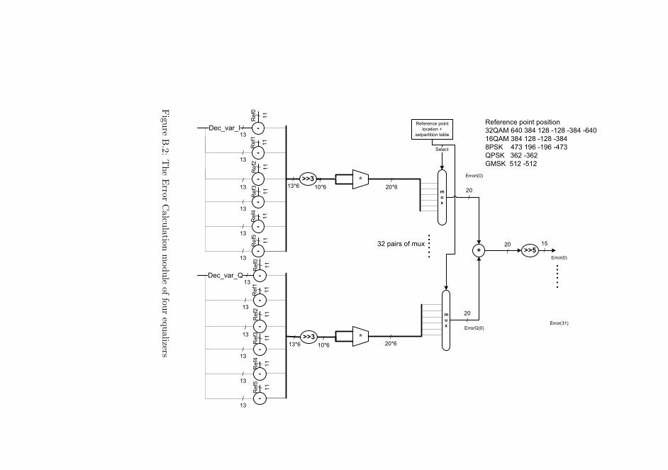
10
1
�
�
�
�
�
�
���������
��
������� �����
�������� �
������������ �����
������
���������
�
��
� �����
�
��
�
����
�
�
�
�
�
�
�
��
�
�
�
����
�� ����� � � !
"�����#�$
"�����#�$
"����#�$
����
"����#��$
������� ����� ��������
���%& '(� �)( ��) *��) *�)( *'(�
�'�%& �)( ��) *��) *�)(
)+�, (-� �.' *�.' *(-�
�+�, �'� *�'�
/&�, ��� *���
����
�
�
�
� ��
�
��
�
��
�
��
�
��
�
��
�
��
�
��
�
��
�
��
�
��
�� � ��
�� � ��
�� � ��
�( � ��
�� � ��
�� � ��
�� � ��
�� � ��
�� � ��
�( � ��
�� � ��
�
��0'
�
��0'
�
��0'
�
��0'
�
��0'
�
��0'
��
�
��
�
Fig
ure
B.2
:T
he
Erro
rC
alcu
latio
nm
od
ule
of
fou
req
ualizers
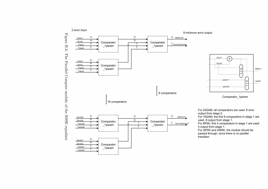
10
2D
iag
ram
so
fth
eeq
ua
lizer
�������
������
�
�
�
�
�
�������
������
������
�����
������
������
���� �
���� �
������
������
���� �
���� �
����������
�������
����������
�������
����������
�������
����
�������
�������
���� ��
���� ��
�������
�������
���� ��
���� ��
����������
�������
����������
�������
����������
�������
�������������
����
������������
�������
����������� �
�������
����������� �
�����������������
���������������������������������
������� !��""����������� ������ �#$���������
�������%���� ������$
������� !��&��%� �������������� ��� �����������
� �#$����������%���� ������$
�����'�(!�%� ��)����������� ��� ������������ �#$�
)��������%���� ������$
�����'�(���#�*�(!��&����#�"�� &��"#�+��
�� �#��&����&!� �����&���� ��������""�"�
���� ���
�,
-�,
-,
-,
-
�,
-�,
-,
-,
-
�,
-�,
-,
-,
-
�,
-�,
-,
-,
-
�,
-�,
- ,
-,
-
�,
-�,
-,
-,
-
�,
-
,
-
�,
-
,
-
Fig
ure
B.3
:T
he
Para
llelC
om
pare
mod
ule
of
the
RS
SE
equ
alizer
Bibliography
[1] J.G.Proakis, “Digital Communications”. McGraw Hill, 4th edition, 2001
[2] G.D.Forney.Jr.,“Maximum-likelihood sequence estimation of digital se-quence in the presence of intersymbol interference”. IEEE Transactions onInformation Theory,VOL.IT-18,pp.363-378,May 1972
[3] A.D.Viterbi, “Error Bounds for Convolutional Codes and Asymptoti-cally Optimum Decoding Algorithms”. IEEE Transactions on InformationTheory,pp.260-269,April 1967.
[4] M.V.Eyuboglu, S.U.H.Qureshi, “Reduced-State Sequence Estimation withSet Partitioning and Decision Feedback”. IEEE Transactions on communi-cations, VOL.36, No.1, January 1988
[5] B.Hassibi and H.Vikalo, “On the Sphere-Decoding Algorithm. I.ExpectedComplexity”. IEEE Transactions on Signal Processing, pp. 2806-2818, Au-gust 2005.
[6] B.Hassibi and H.Vikalo, “On the Sphere-Decoding Algorithm. II. Gener-alizations, Second-Order Statistics, and Application to Communications”.IEEE Transactions on Signal Processing, pp. 2819-2834, August 2005.
[7] 3rd Generation Partnership Project; Technical Specification GroupGSM/EDGE Radio Access Network; Modulation(Release 7) 3GPPTS45.004v7.2.0(2008-02)
[8] 3rd Generation Partnership Project; Technical Specification GroupGSM/EDGE Radio Access Network; Multiplexing and multiple access onthe radio path (Release 7) 3GPPTS45.002 v7.6.0(2007-11)
104 BIBLIOGRAPHY
[9] G Ungerboeck, “Trellis-Coded Modulation with redundant Signal Sets PartI: Introduction”. IEEE communications Magazine February 1987-Vol.25,no2
[10] G Ungerboeck, “Trellis-Coded Modulation with redundant Signal SetsPart II: State of the Art”. IEEE communications Magazine February 1987-Vol.25,no 2
[11] M Hansen, “Comparison of Optimal and Near-Optimal Detection inGSM/EDGE”. Master thesis, Infomatics and Mathematical Modelling,DTU, 2006
[12] K Wu, “Optimal Algorithms for GSM Viterbi Modules”. Master thesis,Infomatics and Mathematical Modelling, DTU, 2003
[13] “Open Core Protocol Specification 2.1” OCP-IP Association 2005
[14] C Langton “Intuitive Guide to Principles of Communications”. Availableon the internet at http://www.complextoreal.com
[15] R. Booth “A note on th application of the Laurent Decomposi-tion to the GSM GMSK signaling waveform”. Tropian, Inc Link:http://www.tropian.com/wps/wselaurent1.pdf
[16] P. J. Ashenden. “The designer’s guide to VHDL”. Morgan Kaufmann, 2ndedition, 2002.
[17] J. F. Wakerly. “Digital design principles and practices”. Prentice Hall, 3rdedition, 2000.
[18] N. H. E. Weste and K. Eshraghian. “Principles of CMOS VLSI design”.Addison Wesley, 2nd edition, 1993.
[19] B. Sklar. “Digital Communications - Fundamentals and Applications”.Prentice Hall ISBN 0-13-211939-0, 2nd edition, 1988.
[20] S. G. Wilson. “Digital Modulation and Coding”. Prentice Hall, 1st edition,10, 1998.