Embed Size (px)
Citation preview

Soft Magnetic Materials and
Devices on Energy Applications
Xing Xing
The Department of Electrical and Computer Engineering
Northeastern University
Boston, Massachusetts
A thesis submitted in partial fulfillment of the requirements for the degree of
Doctor of Philosophy in the field of Electrical Engineering
July, 2011

- 2 -

- 3 -
1 Abstract
The fast development of wireless communication system in recent years has been
driving the development of the power devices from different aspects, especially the
miniaturized volume and renewable power supply, and etc. In this work, we studied the
high frequency magnetic properties of the soft magnetic material -- FeCoB/Al2O3/FeCoB
structures with varied Al2O3 thickness (2nm to 15nm), which would be applied in to the
integrated inductors. Optimized Al2O3 thickness was found to achieve low coercive field
and high permeability while maintaining high saturation field and low magnetic loss.
Three types of on Si integrated solenoid inductors employing the FeCoB/Al2O3
multilayer structure were designed with the same area but different core configurations.
A maximum inductance of 60 nH was achieved on a two-sided core inductor. The
magnetic core was able to increase the inductance by a factor of 3.6 ~6.7, compared with
the air core structures.
Vibration energy harvesting technologies have been utilized to serve as the
renewable power supply for the wireless sensors. In this work, two generations of
vibration energy harvesting devices based on high permeability magnetic material were
designed and tested. The strong magnetic coupling between the magnetic material and the
bias magnetic field leads to magnetic flux reversal and maximized flux change in the
magnetic material during vibration. An output power of 74mW and a working bandwidth
of 10Hz were obtained at an acceleration of 0.57g (g=9.8m/s2) for the 1st generation
design, at 54Hz. An output voltage of 2.52 V and a power density of 20.84 mW/cm3 were

- 4 -
demonstrated by the 2nd generation design at 42 Hz, with a half peak working bandwidth
of 6 Hz.

- 5 -
2 Acknowledgement
I would like to take this opportunity to express my appreciation for my advisor Dr.
Nian Sun, who has provided me the opportunity to pursue research on magnetic material
and energy applications. He has been constantly guiding, supporting and encouraging me,
without which I could not have been writing this dissertation. I sincerely appreciate all of
his advice during my four-year PhD study, because it helped me master the techniques of
solving different kinds of engineering problems and also made me grow.
I would also like to thank my colleagues in the Sun Group at Northeastern
University. Dr. Guomin Yang and Dr. Ming Liu helped me a lot in my first year by
teaching me basic research techniques. Miss Ogheneyunume Obi has offered me help on
all kinds of issues, from paper review to preparing the graduation documents, and they
are so many that I could only recall a small part. These colleagues (Jing Lou, Ziyao Zhou,
Shawn Beguhn, Qi Wang, Zhijuan Su, Jing Wu, Xi Yang, Ming Li) always gave me their
hands when I mostly needed them and they made my four year graduate study an
enjoyable one.
Most importantly, I would like to cherish my gratitude for my parents, who have
always been supporting and loving me unconditionally, and they made me grown up as
an honest and happy person. I would also like to thank my love, Xiaoyu Guo, who has
been supporting me and tolerating everything of mine.
- 6 -
Contents
1 Abstract - 3 -
2 Acknowledgement - 5 -
3 List of Tables - 9 -
4 List of Figures - 10 -
1 Introduction - 19 -
1.1 BASIC MAGNETIC CHARACTERISTICS - 20 -
1.2 HYSTERESIS LOOP AND COERCIVITY - 20 -
1.3 ANISOTROPY - 21 -
1.4 SATURATION MAGNETIZATION - 21 -
1.5 PERMEABILITY - 22 -
1.6 SOFT MAGNETIC MATERIAL - 23 -
1.7 DEVICE APPLICATIONS OF SOFT MAGNETIC MATERIALS - 25 -
REFERENCES - 26 -
2 Experimental Methods - 27 -
2.1 PHYSICAL VAPOR DEPOSITION (PVD) - 27 -
2.2 VIBRATING SAMPLE MAGNETOMETER (VSM) - 29 -
2.3 FERROMAGNETIC RESONANCE (FMR) DETECTION - 32 -
2.4 HIGH FREQUENCY PERMEABILITY MEASUREMENT - 34 -
REFERENCES - 36 -
3 Soft Magnetic Thin Film: FeCoB/Al2O3/FeCoB Structure with Varied
Al 2O3 Thickness - 37 -

- 7 -
3.1 INTRODUCTION - 37 -
3.2 EXPERIMENTAL - 38 -
3.3 HYSTERESIS LOOPS - 39 -
3.4 FMR SIGNALS - 42 -
3.5 PERMEABILITY - 47 -
3.6 CONCLUSION - 50 -
REFERENCES - 51 -
4 Integrated inductors with FeCoB/Al2O3 Multilayer Films - 53 -
4.1 INTRODUCTION - 53 -
4.1.1 QUALITY FACTOR - 54 -
4.1.2 SELF-RESONANCE FREQUENCY - 56 -
4.1.3 DIFFERENT TYPES OF INTEGRATED INDUCTOR - 57 -
4.1.4 THE MAGNETIC CORE - 63 -
4.2 PROTOTYPE AND LAYOUT DESIGN - 65 -
4.3 THEORETICAL MODEL - 71 -
4.3.1 INDUCTANCE - 71 -
4.3.2 RESISTANCE AND SKIN EFFECT - 74 -
4.3.3 LAMINATION CORE LOSS - 76 -
4.3.4 PARASITIC EFFECTS - 77 -
4.3.5 QUALITY FACTOR OF THE SOLENOID TYPE INDUCTORS - 77 -
4.4 ON-CHIP FABRICATION - 78 -
4.5 ON WAFER MEASURING - 88 -
4.5.1 TESTING PLATFORM - 88 -
4.5.2 CALIBRATION - 90 -
4.5.3 PARAMETER EXTRACTION - 92 -
4.6 RESULT AND ANALYSIS - 95 -
4.6.1 NUMBER-OF-TURN DEPENDENCY - 97 -
4.6.2 CORE STRUCTURE DEPENDENCY - 101 -
4.6.3 CONCLUSION - 108 -
REFERENCES - 109 -

- 8 -
5 Soft Magnetic Material Applied Vibration Energy Harvesting - 113 -
5.1 INTRODUCTION - 113 -
5.1.1 AVAILABLE ENERGY SOURCES - 114 -
5.1.2 VIBRATION ENERGY HARVESTING MECHANISMS - 119 -
5.1.3 KEY MATERIALS OF VIBRATION ENERGY HARVESTING DEVICES - 124 -
5.2 WIDEBAND VIBRATION ENERGY HARVESTER WITH HIGH PERMEABILITY MATERIAL - 129 -
5.2.1 INTRODUCTION - 129 -
5.2.2 BASIC MECHANISM - 130 -
5.2.3 PROTOTYPE AND TESTING SYSTEM - 133 -
5.2.4 THEORETICAL MODEL - 134 -
5.2.5 RESULTS AND DISCUSSION - 138 -
5.2.6 NONLINEAR EFFECT - 141 -
5.2.7 ADVANTAGE OF HIGH PERMEABILITY VIBRATION ENERGY HARVESTING - 143 -
5.2.8 SUMMARY - 143 -
5.3 HIGH OUTPUT VIBRATION ENERGY HARVESTER WITH HIGH PERMEABILITY MATERIAL - 144 -
5.3.1 INTRODUCTION - 144 -
5.3.2 BASIC MECHANISM - 145 -
5.3.3 THEORETICAL ANALYSIS - 146 -
5.3.4 PROTOTYPE AND TESTING SYSTEM - 148 -
5.3.5 RESULTS AND DISCUSSION - 149 -
5.3.6 ADVANTAGES OF THE 2ND
GENERATION HIGH PERMEABILITY VIBRATION ENERGY HARVESTER AND
SUMMARY - 153 -
REFERENCES - 154 -
6 Conclusion and Future Work - 158 -

- 9 -
3 List of Tables
Table 1.1 Major families of soft magnetic materials with typical properties. ...... - 24 -
Table 1.2 Representative commercially available magnetic amorphous metals. . - 25 -
Table 3.1 FMR Resonance Field along Easy and Hard Axis at 9GHz, In-plance
Anisotropy, 4πMs and Exchange Coupling Coefficient for Each Sample ... - 46 -
Table 4.1 Performance summary of the various bulk/surface micromachined RF
inductors fabricated on silicon. ..................................................................... - 54 -
Table 4.2 The Design Matrix of the on-Chip Integrated Inductors ...................... - 96 -
Table 5.1 Comparison of different types of available ambient energy sources and
their performance ........................................................................................ - 114 -
Table 5.2 Comparison of several key figures of merit for different vibrating energy
harvesting mechanisms ............................................................................... - 119 -
Table 5.3 Comparison between different materials applied in vibration energy
harvesting system ........................................................................................ - 125 -
Table 5.4 The magnetostriction constants of different soft magnetic materials. - 127 -

- 10 -
4 List of Figures
Fig. 1.1 A typical magnetization hysteresis loop of magnetic materials. ............. - 20 -
Fig. 1.2 A typical hysteresis loop of the magnetic thin film ................................. - 22 -
Fig. 1.3 Chronological summary of major developments of soft magnetic materials. -
23 -
Fig. 2.1. Schematic of magnetron sputtering ........................................................ - 28 -
Fig. 2.2 A picture of the PVD system. .................................................................. - 29 -
Fig. 2.3 A schematic picture of VSM. .................................................................. - 30 -
Fig. 2.4 A picture of the VSM system. ................................................................. - 31 -
Fig. 2.5 The processional motion of the moment M around the static magnetic field
H, before and after the dynamic component h applied. ................................ - 32 -
Fig. 2.6 The FMR signal on (a) the absorbed power vs. static field plot and (b)
dP/dH vs. field plot. ...................................................................................... - 33 -
Fig. 2.7 The permeability measurement system insists of a network analyzer and a
coplanar waveguide. ..................................................................................... - 34 -
Fig. 3.1 (a) Sandwich structure schematic (b) Coercivity of non-annealed sandwich
structures decreases as the insulating alumina thickness increases, indicating
reduced exchange coupling between adjacent FeCoB layers. ...................... - 39 -

- 11 -
Fig. 3.2 (a) The saturation field as a function of the insulator layer thickness, (b) In-
plane hysteresis loop for sandwich with Al2O3 thickness of 2nm and (c) 15nm,
before magnet anneal applied. The saturation field decreases as Al2O3 layer
gets thicker. ................................................................................................... - 40 -
Fig. 3.3 Hysteresis loops of (a) sandwich structure with Al2O3 thickness of 3nm after
annealing, and (b) all samples in large field scale, after magnetic anneal. A
coercive field as low as 0.5Oe was obtained for the trilayer FeCoB(100nm)/
Al 2O3(3nm)/ FeCoB(100nm). High 4πMs value of over 1.5 Tesla was obtained
for all samples. .............................................................................................. - 41 -
Fig. 3.4 FMR signal along easy axis of annealed 200nm single layer FeCoB film and
sandwich layer with Al2O3 of 3nm, at 8.5GHz. ............................................ - 43 -
Fig. 3.5 FMR signals along the easy axis for all samples at (a) 7GHz, (b) 8GHz, (c)
9 GHz and (d) 10 GHz. Optical modes are marked with arrows. ................. - 44 -
Fig. 3.6 Permeability spectrum measured under zero fields for all samples. ....... - 48 -
Fig. 4.2 Equivalent energy model representing the energy storage and loss
mechanisms in a monolithic inductor. Note that Co=Cp+Cs. ....................... - 55 -
Fig. 4.3 The quality factor as a function of frequency. ......................................... - 56 -
Fig. 4.3 (a) Top view and (b) side view of a 3.5-turn square spiral inductor. ...... - 58 -
Fig. 4.4 The equivalent circuit of a spiral inductor. .............................................. - 58 -

- 12 -
Fig. 4.5 Optical microscope images of copper/polyimide based 4-turn elongated
spiral inductor with magnetic material fabricated in a 90 nm CMOS process. ... -
59 -
Fig. 4.6 3-D illustration of the on-chip integrated toroidal inductor. The circled
section represents a unit turn. ........................................................................ - 60 -
Fig. 4.7 Schematic diagrams of (a) the meander type integrated inductor with
multilevel magnetic core and (b) the more conventional solenoid-bar type
inductor. The structure of the two inductor schemes is analogous. .............. - 61 -
Fig. 4.8 Schematic design of an integrated solenoid inductor: (a) top view and (b)
cross-section view. ........................................................................................ - 63 -
Fig. 4.9 Cross sectional SEM image of inductors integrated on an 130 nm CMOS
process with 6 metal levels. Two levels of CoZrTa magnetic material were
deposited around the inductor wires using magnetic vias to complete the
magnetic circuit. ............................................................................................ - 64 -
Fig. 4.10 Inductor design type I. Left top is a schematic top view, where the blue
pads indicate the vias. Left bottom is the 3-D schematic. The red rectangular on
the top is the top layer metal consisting the top layer of the coil, while the blue
rectangular is the bottom layer. The top and bottom metal are connected by vias,
which are in green and yellow. The right picture is the 6-layer layout design
done with Cadence. ....................................................................................... - 65 -

- 13 -
Fig. 4.11 The cross sectional view of inductor type I, shown in Fig. 4.10, along (a)
the transverse direction and (b) longitudinal direction. The yellow parts indicate
the metal, the dark blue parts are the magnetic cores and the light blue area is
the polyimide. The grey part stands for the Si substrates. ............................ - 66 -
Fig. 4.12 The schematic drawn of inductor type II, the top view (left top), 3-D view
(left bottom) and a 6-layer layout of a 10-turn structure (right). .................. - 67 -
Fig. 4.14 The schematic pictures of inductor type III, the top view (left top), 3-D
view (left bottom), and a 6-layer layout of a 10-turn device. ....................... - 68 -
Fig. 5.14 The layout design of an 8-turn inductor Type I (upper) and its open
structure with only the contour ground structure and the testing pads (lower).
The cross arrays in the open area are the aligning marks. ............................ - 69 -
Fig. 4.16 Layout design of the testing structures, including the via resistance testing
bars, polyimide step monitor, precision monitor and sheet resistance testing
pads. .............................................................................................................. - 70 -
Fig. 4.16 Self inductance value for a rectangular conductor versus its length and
width (the thickness is fixed at 1µm). ........................................................... - 72 -
Fig. 4.17 Equivalent circuit of an integrated inductor. ......................................... - 78 -
Fig. 4.18 A 10µm thick polyimide layer was coated on the Si substrate. ............. - 79 -
Fig. 4.19 A seedlayer was deposited with PVD, for the bottom metal. ................ - 79 -
Fig. 4.20 A thick photoresist layer was patterned above the seedlayer. ............... - 80 -
- 14 -
Fig. 4.21 Electric plating of the bottom coils and the removal of PR................... - 80 -
Fig. 4.22 The schematic view of the wafer (upper) and a zoom-in picture of the real
wafer (lower) after the Cr/Cu seedlayer removed. ........................................ - 81 -
Fig. 4.23 Polyimide layer-2 coating and patterning. ............................................. - 82 -
Fig. 4.24 Photoresist layer coating and patterning for the magnetic lift-off process. .. -
82 -
Fig. 4.25 Schematic view of the lift-off process (upper), and pictures of the lift-off
patterned cores (lower). ................................................................................ - 83 -
Fig. 4.26 Polyimide layer-3 was spin coated above the magnetic layer, and patterned
to have the via openings. ............................................................................... - 84 -
Fig. 4.27 (a) A seedlayer (Cr/Cu) was deposited above PI3 layer. (b) The re-sputter
process is able to re-distribute the seedlayer in the via openings during the
deposition. ..................................................................................................... - 85 -
Fig. 4.28 An 8 µm thick photoresist layer was coated and patterned above the
seedlayer ....................................................................................................... - 86 -
Fig. 4.29 After the top metal layer plated, the photoresist was stripped with acetone.
The seedlayer was removed as discussed earlier. ......................................... - 86 -
Fig. 4.30 Picture of the on-chip inductors, Type I, type II and Type III respectively. -
87 -

- 15 -
Fig. 4.31 (a) The GSG probes are mounted on the arms of two micropositioners
which can be controlled by the (b) probe station. Meanwhile, they are
connected to the two ports of the vector network analyzer through the low loss
coaxial cables. ............................................................................................... - 89 -
Fig. 4.32 The SOLT calibration procedure includes four steps: Measuring the short,
open, load and through standard. .................................................................. - 91 -
Fig. 4.33 Three possible configurations for measuring a two-port device ZL with a
VNA. They are two-port measurement with the device placed in series with the
ports, two-port measurement with the device placed in parallel with the ports,
and one-port measurement, respectively from left to right. .......................... - 92 -
Fig. 4.34 Setup for the calculation of the scattering parameters of a two-port
measurement with the Π model. ................................................................... - 93 -
Fig. 4.35 The measured inductance and quality factor of inductor type I, for different
numbers of turns. .......................................................................................... - 98 -
Fig. 4.36 The measured inductance and quality factor of inductor type II, for
different numbers of turns. ............................................................................ - 99 -
Fig. 4.37 The measured inductance and quality factor of inductor type III, for
different numbers of turns. .......................................................................... - 100 -
Fig. 4.38 The inductance plots for different core types, with the same numbers of
turns. (a) N=6; (b) N=8: (c) N=10 (d) N=12; (e) N=14. ............................. - 104 -

- 16 -
Fig. 4.39 The quality factor plots for different core types, with the same numbers of
turns. (a) N=6; (b) N=8: (c) N=10 (d) N=12; (e) N=14. ............................. - 107 -
Table 5.1 Comparison of different types of available ambient energy sources and
their performance ........................................................................................ - 114 -
Fig. 5.1 Power-generation mode of thermoelectric material .............................. - 116 -
Fig. 5.2 Figure of merit ZT as a function of temperature for several bulk
thermoelectric materials. ............................................................................. - 117 -
Fig. 5.3 In-plane overlap varying. ....................................................................... - 122 -
Fig. 5.4 In-plane gap closing............................................................................... - 122 -
Fig. 5.5 Out-of-plane gap closing. ...................................................................... - 122 -
Fig. 5.6 Electromagnetic energy harvesting mechanism. ................................... - 123 -
Fig. 5.7 The section view of the schematic design of the vibration energy harvesting
device. Dimension of each part is: 4.4cm ×3.2cm×4cm for the solenoid,
1.25cm×2.2cm×1.5cm for the magnet pair including the gap in between,
1.3cm×1.5cm×2.5cm for the mounting frame on one side and
0.5cm×1.5cm×0.6cm on the other. ............................................................. - 130 -
Fig. 5.8 Magnet pair with antiparallel magnetic moment provides closed magnetic
field lines, making sure the maximum magnetic flux change, from Φ to –Φ
during the vibration. .................................................................................... - 131 -

- 17 -
Fig. 5.9 Magnet pair with parallel magnetic moment provides repelling magnetic
field lines, in which case the magnetic flux changes from Φ to 0 and back to Φ
during the vibration. .................................................................................... - 132 -
Fig. 5.10. Prototype of the wideband high permeability vibration energy harvester. .. -
133 -
Fig. 5.11. The Schematic of the calculation of induced voltage across the solenoid. . -
134 -
Fig. 5.12 Hysteresis loop of the MuShield beam with the dimension of 4.6cm ×
0.8cm × 0.0254cm. ..................................................................................... - 135 -
Fig. 5.13. Beam shape at its maximum deflection. ............................................. - 136 -
Fig. 5.14 Measured and calculated results of the open circuit voltage for the energy
harvesting device at the mechanical vibration frequency 54 Hz, acceleration
0.57 g (g=9.8 m/s2). .................................................................................... - 139 -
Fig. 5.15 Normalized magnetic flux as a function of time and free end amplitude, at
vibration frequency of 54 Hz, acceleration 0.57 g. ..................................... - 140 -
Fig. 5.16 Measured and calculated frequency response of the energy harvester.- 140
-
Fig. 5.17 Elastic potential energy, magnetic potential energy and total potential
energy of the oscillation system as functions of free end displancement of the
beam. ........................................................................................................... - 141 -

- 18 -
Fig. 5.18 The schematic design and working mechanism of the high power vibration
energy harvester. (a) The magnet pair moves to the top. (b) The magnet pair
moves to the bottom. ................................................................................... - 146 -
Fig. 5.19 Structure of the vibration energy harvester. Dimension of each component
is: 2 × 2.5 × 1 cm3 for the solenoids, 1.25 × 2.2 × 1.5 cm3 for the magnetic pair,
including the gap in between. ..................................................................... - 149 -
Fig. 5.20 Measured results of the open circuit voltage for the energy harvesting
device with three different springs at respective resonance frequencies: spring
#1 at 27 Hz; spring #2 at 33 Hz and spring #3 at 42 Hz. ............................ - 150 -
Fig. 5.21 Measured maximum output power of the harvester with three different
springs, at resonance frequency of each. .................................................... - 151 -
Fig. 5.22 Measured output power spectrum of the harvester with spring #3.
Maximum output is 610.62 mW, obtained at 42 Hz, corresponding to a volume
density of 20.84 mW/cm3. This curve shows a half-peak working bandwidth of
6 Hz. ............................................................................................................ - 152 -

- 19 -
1 Introduction
Magnetic materials are traditionally classified by their volume magnetic
susceptibility, χ which represents the relationship between the magnetization M and the
magnetic field H strength, M=χH. The first type is diamagnetic, for which χ is small and
negative χ≈ −10−5and its magnetic response opposes the applied magnetic field.
Examples of diamagnetics are copper, silver, gold, and etc. Superconductors form
another special group of diamagnetics whose χ≈−1. The second group has small and
positive susceptibility, χ≈10−3∼10−5 called paramagnets. It has w eak magnetization but
aligned parallel with the bias magnetic field. Typical paramagnetic materials are
aluminum, platinum and manganese. The most widely recognized magnetic materials are
the ferromagnetic materials, whose susceptibility is positive and much greater than 1,
χ≈50 to 10000. Examples of ferromagnetic material are iron, cobalt, nickel and several
rare earth metals. [1.1]
Based on the coercivity, ferromagnetic materials are divided in to two groups.
One is called “hard” magnetic material, with coercivity above 10 kA m-1; the other group
is call “soft” magnetic material, whose coercivity is below 1 kA m-1.
Ferromagnetic materials are widely applied in different aspects of everyday life
and work, such as permanent magnets, electrical motors, magnetic recording, power
generation, energy harvesting, and inductors.

- 20 -
1.1 Basic Magnetic Characteristics
The mostly desired essential characteristics for all soft magnetic materials are high
permeability, low coercivity, high saturation magnetization and low magnetic loss.
1.2 Hysteresis Loop and Coercivity
In an external magnetic field H, the magnetic material gets magnetized and shows a
finite spontaneous magnetization M. In the MKS unit, total magnetic flux B=µ0Η+M ,
Figure 1.1 shows a typical H vs. M magnetization hysteresis curve of a magnetic material.
For a
Fig. 1.1 A typical magnetization hysteresis loop of magnetic materials.

- 21 -
soft magnetic material, M follows H readily; with a high relative permeability µ=Β/µ0Η.
Soft magnetic materials differ from hard magnetic materials for their much smaller
coercivity values.
1.3 Anisotropy
The dependence of magnetic properties on a preferred direction is called magnetic
anisotropy. Different types of anisotropy include: magnetocrystalline anisotropy, shape
anisotropy and magnetoelastic anisotropy.
Magnetocrystalline anisotropy depends on the crystallographic orientation of the
sample in the magnetic field. The magnetization reaches saturation in different fields.
Shape anisotropy is due to the shape of a mineral grain. A magnetized body produces
demagnetizing field which acts in opposition to the applied magnetic field.
Magnetoelastic anisotropy arises from the strain dependence of the anisotropy
constants. A uniaxial stress can produce a unique uniaxial anisotropy.
The anisotropy constant K is defined as the volume density of anisotropy energy Ea.
The anisotropy field is the magnetic field needed to rotate the magnetization direction in
the hard direction. Hk of a magnetic film can be read on the hysteresis loop along the hard
axis, in Fig. 1.2.
1.4 Saturation Magnetization
The saturation magnetization is defined as the volume density of maximum induced
magnetic moment, which can be shown on the hysteresis loop. The saturation

- 22 -
magnetization 4πMs of the magnetic thin film can be read directly from the hysteresis
loop measured along the out-of-plane direction, shown in Fig. 1.2.
Fig. 1.2 A typical hysteresis loop of the magnetic thin film.
1.5 Permeability
The magnetic permeability describes the relation between magnetic field and flux,
B=µH, and µ=µ0µr, where µr is the relative magnetic permeability. Also, the relative
magnetic permeability is related to the susceptibility by χ=µr−1. With the values of Hk

- 23 -
and 4πMs, which can be read from the hysteresis loops, the permeability of a magnetic
thin film could be evaluated by =
+ 1.
1.6 Soft Magnetic Material
Fig. 1.3 Chronological summary of major developments of soft magnetic materials.

- 24 -
Soft magnetic materials are economically and technologically the most important
of all magnetic materials, and they have been used to perform a wide variety of magnetic
functions. Some applications demand high permeability; others emphasize low energy
loss at high frequencies. [1.2] Figure 1.3 shows a chronological summary of major
developments of soft magnetic materials. [1.3]
From the beginning of the 19th century, research has been focused on the developing
of higher permeability µ, saturation magnetization Ms and lower coercivity Hc. The
advent of rapid solidification technology (RST) in the 1970s and 1980s provided
metallurgists a route to novel compositions and microstructures.[1.4] Amorphous metals
(also called metallic glasses) produced by RST were arguably the most important
development in soft magnetic materials. Four major families of soft magnetic materials
are: electrical steels, FeNi and FeCo alloys, ferrites, amorphous metals, and the typical
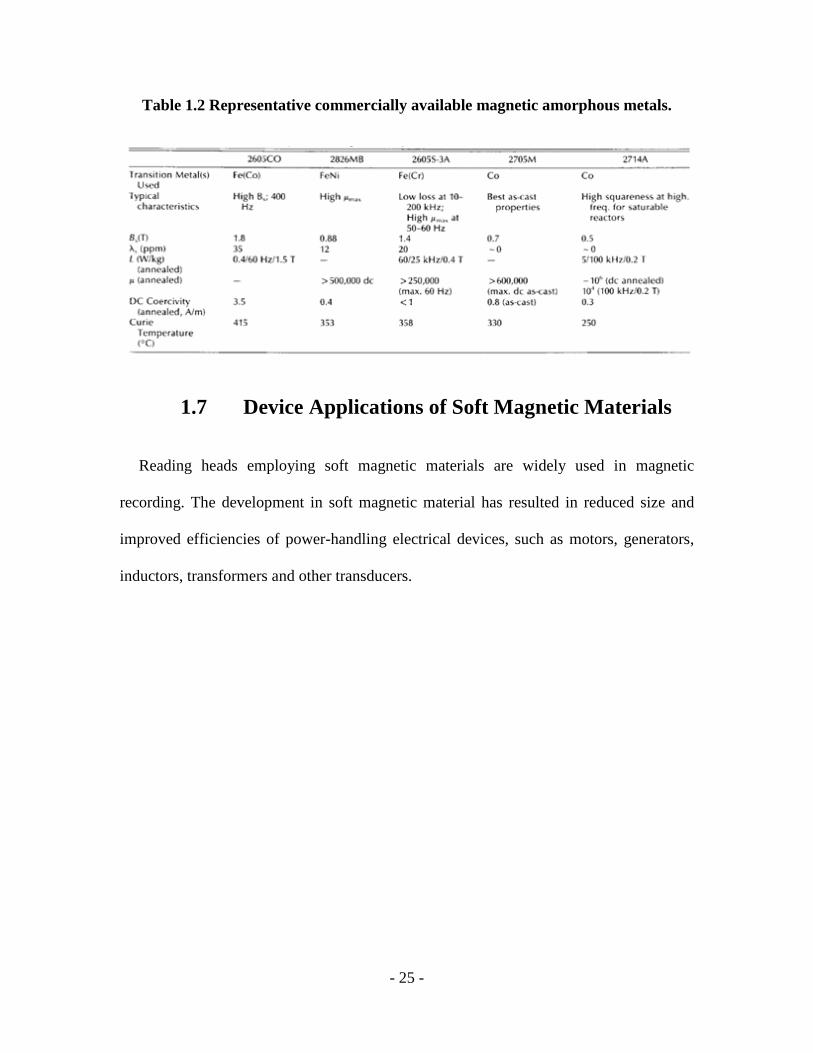
properties are shown in Table 1.1 and 1.2.[1.5]
Table 1.1 Major families of soft magnetic materials with typical properties.
- 25 -
Table 1.2 Representative commercially available magnetic amorphous metals.
1.7 Device Applications of Soft Magnetic Materials
Reading heads employing soft magnetic materials are widely used in magnetic
recording. The development in soft magnetic material has resulted in reduced size and
improved efficiencies of power-handling electrical devices, such as motors, generators,
inductors, transformers and other transducers.

- 26 -
REFERENCES
1.1 D. Jiles, “Introduction to Magnetism and Magnetic Materials”, 2nd Edition, (1998).
1.2 C. W. Chen, “Magnetism and Metallurgy of Soft Magnetic Materials”, (1986).
1.3 Bechtold and Wiener, (1965).
1.4 S. K. Das and L. A. Davis, Mater. Sci. Eng., VOL. 98, 1, (1988).
1.5 G. E. Fish, Soft Magnetic Material, Proceedings of the IEEE, VOL. 78, NO. 6, June
(1990).

- 27 -
2 Experimental Methods
The self-made soft magnetic films used in this research were deposited by DC or
RF magnetron sputtering, which is a physical vapor deposition (PVD) technique.
The magnetostatic properties of these magnetic films were measured with the
vibrating sample magnetometer (VSM).
2.1 Physical Vapor Deposition (PVD)
Physical vapor deposition denotes the vacuum deposition processes, such as
evaporation, sputtering, ion-plating, and ion-assisted sputtering. During the deposition,
the coating material switches into a vapor transport phase, which does not generally rely
on chemical reactions but by physical mechanism. In the current semiconductor industry,
PVD technology is entirely based on physical sputtering.
During the magnetron sputtering process, the substrate is placed between two
electrodes in a low-pressure, ~10-7 Torr, vacuum chamber. The electrodes are driven by
an RF power source, which generates plasma and ionized the rare gas (such as argon)
between the electrodes. A DC bias voltage is used to drive the gas ions towards the
surface of the cathode, which contains a target material, and knock off atoms from the
surface. The free atoms then condense on the substrate surface to form a thin film. A

- 28 -
strong magnetic field is applied to contain the plasma near the surface of the target to
increase the deposition rate. Figure 2.1 shows the schematic of magnetron sputtering.[2.1]
Figure 2.2 is the picture of the PVD system used to make all the self-made magnetic
materials in this work.
Fig. 2.1. Schematic of magnetron sputtering.

- 29 -
Fig. 2.2 A picture of the PVD system.
2.2 Vibrating Sample Magnetometer (VSM)
A vibrating sample magnetometer (VSM) is an instrument that is used to measure
the magnetostatic properties of magnetic films. As shown in Fig. 2.3 [2.2], a VSM pick-up
coil transducer, a lock-in amplifier, a gaussmeter and a controller. The electromagnet pair
provides the magnetizing DC field. The piezoelectric oscillator physically vibrates the
sample in the magnetic field at a fixed sinusoidal frequency. The motion of the sample

- 30 -
relative to the magnetic field modulates the magnetic flux, which is generally consists of
Fig. 2.3 A schematic picture of VSM.
an electromagnet pair, a piezoelectric mechanical oscillator, picked up by the detection
coil. The detection coil generates the signal voltage due to the changing flux emanating
from the vibrating sample. The lock-in amplifier is used to measure the voltage relative to
the piezoelectric oscillation. The gaussmeter measures the applied DC magnetic field.
The output is usually the magnetic moment M or flux B as a function of the field H. The
picture of a VSM system is shown in Fig. 2.4. The entire system also consists of the
power regulator and a computer interface.

- 31 -
Fig. 2.4 A picture of the VSM system.

- 32 -
2.3 Ferromagnetic Resonance (FMR) Detection
When a bias static magnetic field H is present, the magnetization vector M keeps
the damped precession motion around H due to the magnetic torque until it gets aligned
to the same direction because of the existence of the damping. The Gilbert form of
damping is used to describe the relaxation mechanism. This equation takes the form:
= − × +
×
, (2.1)
where γ is the gyromagnetic ratio and α represents the Gilbert damping parameter.
Fig. 2.5 The processional motion of the moment M around the static magnetic field H,
before and after the dynamic component h applied.

- 33 -
If the magnetic field contains a dynamic component h whose frequency equals the
intrinsic frequency of the damping, the energy provided by the dynamic h compensates
the damping loss during the precession. In this case, the magnetization vector M keeps
rotating around H, as shown in Fig. 2.5. [2.3]
In the FMR measurement, the microwave signal is usually used as the dynamic
magnetic field source. A complete testing system includes an electro-magnet pair, an AC
coil, a lock-in amplifier, a coplanar waveguide, a crystal signal detector and a computer.
The electro-magnet is able to generate large bias magnetic field, up to Tesla range. The
AC coil provides a small AC magnetic field, and it is usually controlled by the output end
of lock-in amplifier applying an AC current. The magnetic thin film is placed in the
center area of the coplanar waveguide, where the film interfaces with the microwave
signal. The output microwave signal at the other end is received by the detector. The
(a) (b)
Fig. 2.6 The FMR signal on (a) the absorbed power vs. static field plot and (b) dP/dH vs. field plot.
effect of the magnetic film could be seen by drawing the absorption curve of the
microwave, as shown in Fig. 2.6 (a). Also, by doing the derivative of the absorbed energy

- 34 -
over the magnitude of the magnetic field, the linewidth could be easily read from the plot,
shown in Fig. 2.6(b).
2.4 High Frequency Permeability Measurement
The complex permeability of magnetic materials, µ=µ'-jµ'', is a very important
magnetic characteristic under AC magnetic field. In order to meet the requirement of the
miniaturization of electronics, the working frequency of magnetic materials has been
increasing. At low frequency ranges, the permeability could be measurement by
Fig. 2.7 The permeability measurement system insists of a network analyzer and a coplanar
waveguide.

- 35 -
wrapping coils around the magnetic material. However, when it comes to MHz range, the
parasitic capacitor due to the coils and the increased loss in the wires make the old
method invalid.
New high-frequency permeameters have been developed to extract the frequency
profile of the complex permeability of thin films at high frequencies. The testing system
consists of a transmission line and a network analyzer, as shown in Fig. 2.7. Only the
reflection and transmission parameter can be used to extract the permeability in the
frequency domain. A pick-up coil working as a signal sensor is able to increase the
sensitivity in low-frequency ranges. Figure 2.3 shows a typical permeability testing
platform.
After getting the s-parameters from the network analyzer, the permeability can be
simply obtain by
, (2.2)
where l, t, µ0, ω0, and Zo are the sample length, sample thickness, permeability constant,
angular frequency, and characteristic impedance of the fixture respectively. A scaling
factor k (0.1 ≤ k ≤ 1) is determined from curve fitting and extrapolation of the relative
permeability back to =
+ 1 at zero bias and frequency ~ 0 Hz.

- 36 -
REFERENCES
2.1 M. Liu, “E-field Tuning of Magnetism in Multiferroic Heterostructures”, PhD thesis,
May (2010).
2.2 http://members.aol.com/RudyHeld/publications/unpublished/VSM/vsm.htm
2.3 J. A. Weil, J. R, Bolton, and J. E. Wertz, “Electron Paramagnetic Resonance:
Elementary Theory and Practical Applications”, Wiley-Interscience, New York, (2001).

- 37 -
3 Soft Magnetic Thin Film:
FeCoB/Al2O3/FeCoB Structure with
Varied Al 2O3 Thickness
In this work, we studied the effects of the Al2O3 layer thickness on the RF
magnetic properties of FeCoB(100nm)/Al2O3/FeCoB(100nm) sandwich structure, by
measuring the magnetization hysteresis loop, FMR linewidth and permeability spectrum
of each sample under different conditions.
3.1 Introduction
Magnetic/insulator multilayer films have attracted considerable interest. They
show significantly reduced eddy current loss, and reduced out of plane anisotropy
compared to single layer metallic magnetic films. A typical sandwich system is
composed of two ferromagnetic layers with a non-magnetic interlayer in between.
Numerous experiments have been done to understand the interlayer interaction of
ferromagnetic layers through intermediate non-magnetic insulating layers, which in many
instances determine various magnetic properties of the metallic magnetic films. The
magnetic/insulator multilayer structures provide great opportunities for RF magnetic
devices such as integrated magnetic inductors and transformers. Amorphous Fe70Co30B

- 38 -
films have been reported to have a high magnetization, low coercivity, high permeability
and low magnetic loss at high frequency. Laminated FeCoB/insulator multilayer
constitutes great core materials for integrated magnetic inductors. High magnetization [3.1,
3.2], low coercivity and large magnetic/insulator thickness ratio are preferred for achieving
high effective permeability in the magnetic/insulator multilayer core. However, the
thickness of the insulator layer is directly linked to the domain states of the multilayer [3.3]
and is limited by the interlayer exchange coupling [3.4, 3.5, 3.6], causing high coercivity and
large RF loss tangent. In addition, the insulator in metallic magnetic/insulator multilayer
need to be thick enough so that it is pin hole free.
3.2 Experimental
The samples were prepared using the PVD (Physical Vapor Deposition) system;
by DC sputtering the Fe70Co30 target and RF sputtering the B and Al2O3 targets at room
temperature onto Si substrates to make the sandwich structure
FeCoB(100nm)/Al2O3/FeCoB(100nm), and single layer FeCoB(200nm). The base
pressure of the sputter system was 10-8 Torr. The thickness of the alumina layer was
varied from 2nm to 15nm. Deposition rate of each layer was determined from the
sputtering time vs. film thickness plot, which was evaluated by Dektak profilometer and
NanoSpec optical spectrometer. A postannealing process was performed in a magnetic
field of about 200Oe at 300oC for 5 hours in the same PVD system vacuum chamber.
Magnetization curve of the samples before and after the magnetic anneal were measured
by a Vibrating Sample magnetometer (VSM). The ferromagnetic resonance absorption
signals were tested with a field-swept ferromagnetic resonance testing system.

- 39 -
Permeability spectrum was measured with a microwave network analyzer.
Fig. 3.1 (a) Sandwich structure schematic (b) Coercivity of non-annealed sandwich structures decreases as the insulating alumina thickness increases, indicating reduced
exchange coupling between adjacent FeCoB layers.
3.3 Hysteresis Loops
Figure 3.1(b) shows the coercivity of the FeCoB(100nm)/Al2O3/FeCoB(100nm)
trilayers as a function of Al2O3 thickness before magnetic annealing. The schematic of
the sandwich structure is shown in inset (a) of Fig. 3.1. The coercive fields drastically
decreased from 5Oe to 0.5Oe as the alumina thickness (dA) increased from 2nm to 6nm,
and remained below 0.5Oe up to a dA of 15nm. Higher coercive fields at lower
thicknesses (below 6nm) indicate the existence of interlayer coupling between the

- 40 -
ferromagnetic layers. As the Al2O3 thickness is increased from 2nm to 6nm, the interlayer
Fig. 3.2 (a) The saturation field as a function of the insulator layer thickness, (b) In-plane hysteresis loop for sandwich with Al2O3 thickness of 2nm and (c) 15nm, before magnet
anneal applied. The saturation field decreases as Al2O3 layer gets thicker.
coupling degrades, resulting in a significant decrease in the in-plane coercive field of the
sandwich structure.
Figure 3.2(a) displays the saturation field of magnetization curves as a function of
Al 2O3 thickness from 2nm to 15nm. Higher saturation fields at lower dA indicate a
stronger interlayer coupling for the trilayer structure. In the antiferromagnetic coupled
region, a typical magnetization hysteresis loop for dA=2nm is shown in inset (b) of Fig.
3.2. With further increase of dA, from 6nm to 15nm, the interlayer coupling transits to the

- 41 -
ferromagnetic coupled region, for which the magnetization curve is shown in inset (c) of
Fig. 3.2. The conclusion of antiferromagnetic coupling from Fig. 3.2 agrees with that
observed from Fig. 3.1.
After annealing, the coercive field along the easy axis still follows the same trend as
shown in Fig. 3.1(a). Somewhat differently, it drops below 0.5Oe in the case of dA=3nm
and the magnetization curve is shown in Fig. 3.3(a). Out of plane magnetic hysteresis
loops of all samples are nearly identical both before and after annealing, as shown in Fig.
3.3(b), indicating a large saturation magnetization, 4πMs, value over 1.5Tesla. It could be
Fig. 3.3 Hysteresis loops of (a) sandwich structure with Al 2O3 thickness of 3nm after
annealing, and (b) all samples in large field scale, after magnetic anneal. A coercive field as
low as 0.5Oe was obtained for the trilayer FeCoB(100nm)/ Al2O3(3nm)/ FeCoB(100nm).
High 4ππππMs value of over 1.5 Tesla was obtained for all samples.

- 42 -
concluded that the critical Al2O3 thickness at which the antiferromagnetic coupling
transfers to ferromagnetic coupling for annealed trilayer film is between 3nm to 6nm.
3.4 FMR Signals
The ferromagnetic resonance (FMR) reflects the dynamic process of
magnetization and the motion of magnetic dipoles can be described by the following
form of the Landau-Lifshitz equation:
dt
dMM
MHM
dt
dM ×−×= αγ )( , (3.1)
where M and H represent the magnetization and the magnetic field respectively, γ is the
gyromagnetic constant and α is the damping factor. The FMR linewidth of the annealed
single layer FeCoB(200nm) film and all sandwich structures were measured. The
sandwich structure of FeCoB(100nm)/Al2O3/FeCoB(100nm) is expected to solve two
significant problems which exist in single layer films [3.7]. One problem is the
complicated magnetic domain structure which appears typically in single layer films. In
order to form closure magnetic domain configuration, local magnetization in magnetic
domains in particular on the edge of the film orients along the edge, not always parallel to
the easy direction. The magnetic coupling between the neighboring FeCoB films can
eliminate this domain structure. Another problem with single layer films is the larger
magnetic loss due to the higher thickness. The inserted insulator spacer divides the
thicker single layer into two thinner ones, in which the eddy current loss is decreased.
FMR signal of the sample with dA=3nm is shown in Fig. 3.4, in which the linewidth is
29Oe, compared to 50Oe of a single FeCoB (200nm) layer, at 8.5GHz.

- 43 -
Fig. 3.4 FMR signal along easy axis of annealed 200nm single layer FeCoB film and sandwich layer with Al2O3 of 3nm, at 8.5GHz.
In order to further study the interlayer coupling and magnetic loss within the
sandwich structures, FMR signals were measured along the easy axis at 7GHz, 8GHz,
9GHz and 10GHz, respectively, as shown in Fig. 3.5. The acoustic mode appears at a
certain value of magnetic field H, which is determined by two equations
)4)((, saHAFMR MHHHf πγ +−=+(hard axis) (3.2)
)4)((, asaEAFMR HMHHHf +++=+ πγ (easy axis) (3.3)
where Ms is the saturation magnetization of each FeCoB layer. H is the applied magnetic
field. Ha is the in-plane uniaxial anisotropy field, induced by the magnetic annealing.
With equation (3.2) and (3.3), Ha and 4πMs were calculated from the FMR field along

- 44 -
Fig. 3.5 FMR signals along the easy axis for all samples at (a) 7GHz, (b) 8GHz, (c) 9 GHz and (d) 10 GHz. Optical modes are marked with arrows.

- 45 -
easy and hard axis for each sample at 9GHz, shown in Table 3.1. Equation (3.2) and (3.3)
also indicate that as frequency increases the resonance peak moves to higher magnetic
field. The main FMR peak is the acoustic resonance mode, referring to the in-phase
precession between the neighboring ferromagnetic layers. [3.8] Optical mode could also be
predicted by these two equations [3.9]
)4)((, effeffaHAFMR JMHJHHf −+−−=− πγ (hard axis) (3.4)
)4)((, effaeffaEAFMR JHMHJHHf −++−+=− πγ (easy axis) (3.5)
dMJJ ereff /2 int−= (3.6)
Where Jinter is the interlayer exchange coupling constant, and d is the thickness of a single
ferromagnetic layer. The optical modes were observed for sandwich structures with
Al 2O3 thickness below 6nm, and it represents out-of-phase precession. [3.10] Equation
(3.2) and (3.3) gave a straight forward relationship
effacousticoptical JHH += . (3.7)
The interlayer exchange coupling is determined by the term Jeff. A positive Jeff indicates a
antiferromagnetic coupling whereas a negative Jeff represents a ferromagnetic coupling.
[3.11] In Fig. 3.5, all optical modes are located at a higher field than their acoustic signals,
showing positive Jeff and antiferromagnetic coupling. The existence of optical modes in
sandwich structures with Al2O3 thickness below 6nm also indicates that the interlayer
antiferromagnetic coupling only happens in trilayers with thinner insulating layers. The
interlayer exchange coupling coefficient Jeff for each sample, and the distance between the

- 46 -
acoustic mode and the optical mode are shown in Table 3.1. All positive values
correspond to antiferromagnetic coupling, which agree with earlier conclusions. It is
interesting to notice that the optical mode is much weaker than its acoustic mode.
Although it does not decrease monotonically with the Al2O3 thickness, it tends to get
closer to the acoustic peak in thicker Al2O3 cases, indicating weaker coupling in samples
Table 3.1 FMR Resonance Field along Easy and Hard Axis at 9GHz, In-plance Anisotropy,
4ππππMs and Exchange Coupling Coefficient for Each Sample
Al 2O3
(nm) HEA(Oe)
HHA(Oe) Ha(Oe) 4πMs(Tesla) Jeff(Oe)
2 589.8 618.7 14 1.65 64.6
3 609 629.4 10.4 1.61 57.3
4 609.7 633.6 12.2 1.6 83.7
6 611.1 631.9 10.6 1.6 62.2
10 611.1 629.3 9.3 1.6 0
15 608.1 628.8 10.5 1.61 0

- 47 -
with thicker insulator layers. This also means that the ferromagnetic coupling switches to
antiferromagnetic coupling faster in field when the insulating layer gets thicker.
The measured FMR linewidth of each sample is pretty close, but slightly
increases as the Al2O3 thickness decreases. At 9GHz, the linewidth of the sandwich with
Al 2O3 of 15nm is 33.2Oe, while that with Al2O3 of 2nm is 34.8Oe.
As seen in all curves of Fig. 3.5, there is a 2nd FMR signal located on the lower field
side of the main peak, which is a standing spin wave. It also shifts to upper field positions
at higher frequency. The spin wave mode could be described as
)/(2 222 dMAnHH sn π−= , (3.8)
where nH is the required static field for exciting a particular spin-wave mode with order
number n. A is the exchange constant, related to the exchange coupling [3.12]. The uniform
processing mode corresponds to the case of n=0. The standing spin wave modes observed
in Fig. 3.5 are most likely the case of n=1, which are the fist modes to the lower field side
of the main peaks. d is the thickness of the film. From equation (3.8), it is clear that the
standing spin wave moves to higher field location with the uniform mode when the
frequency increases. The standing spin wave is due to the coupling of the surface spin-
wave modes of two adjacent magnetic layers, when the degeneracy of the FMR signals is
lifted [3.13].
3.5 Permeability
Figure 3.6 exhibits the change of permeability of the trilayers as a function of
frequency. The real part of permeability is maintained above 600 for all samples, up to
about 1GHz. The imaginary part indicate a zero field resonance frequency around
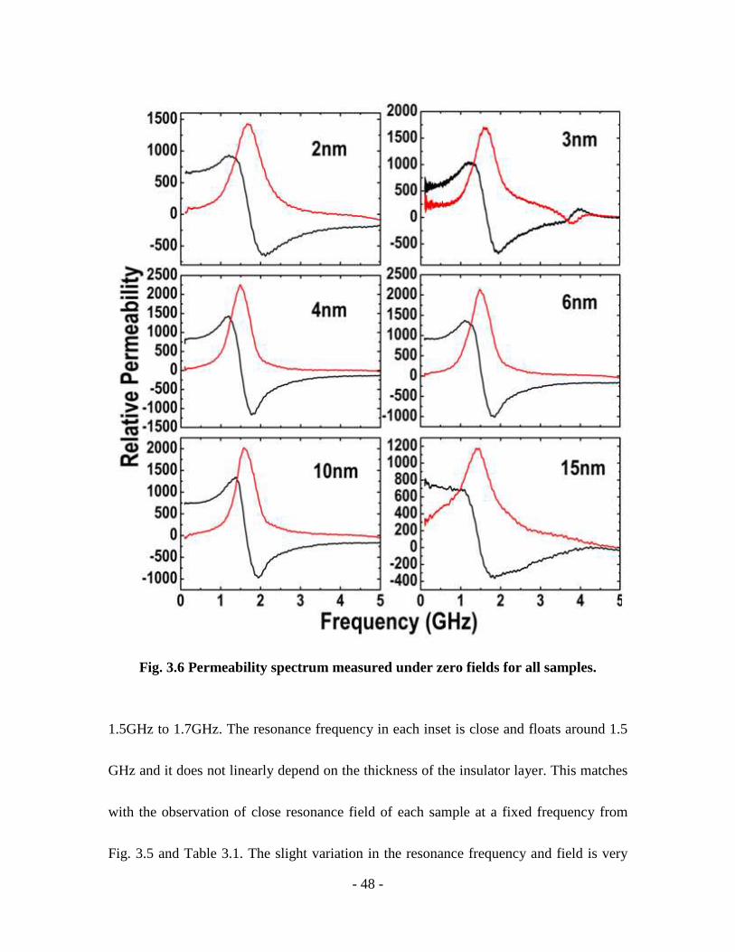
- 48 -
Fig. 3.6 Permeability spectrum measured under zero fields for all samples.
1.5GHz to 1.7GHz. The resonance frequency in each inset is close and floats around 1.5
GHz and it does not linearly depend on the thickness of the insulator layer. This matches
with the observation of close resonance field of each sample at a fixed frequency from
Fig. 3.5 and Table 3.1. The slight variation in the resonance frequency and field is very

- 49 -
likely related to the perturbation on the deposition environment of each sample, such as
the temperature and pressure. Also, it is interesting to notice a higher order mode in the
3nm case, which is due to spin wave resonance along the thickness direction [3.14]. This
means that the spin wave resonance is observed in both frequency-swept and field-swept
FMR measurements, therefore mutually confirmed.

- 50 -
3.6 Conclusion
Magnetization hysteresis loops, FMR curves and permeability spectrum were
measured for a series of FeCoB(100nm)/Al2O3/FeCoB(100nm) sandwich structures with
varied Al2O3 thickness. The coercive force dropped below 0.5Oe when the Al2O3
thickness increases above 3nm, indicating the transition of interlayer antiferromagnetic
coupling to ferromagnetic coupling. The appearance of the optical modes in the FMR
curves for the samples with thin Al2O3 layers also identified the antiferromagnetic
coupling. The FMR linewidth of the sandwich structure was found to be much lower than
that of a 200nm single layer FeCoB film. The permeability spectrums were tested to
show high permeability of above 600 up to from 1.5GHz to 1.7GHz. The low coercive
force, high 4πMs, narrow FMR linewidth and high permeability at high frequency region,
make FeCoB(100nm)/Al2O3/FeCoB(100nm) structure a good candidate of RF device
applications, which require soft magnetic films with high saturation magnetization and
low magnetic loss.

- 51 -
REFERENCES
3.1 S. X. Wang, N. X. Sun, M. Yamaguchi and S. Yabukami, “Sandwich Films: Properties
of a New Soft Magnetic Material,” Nature, VOL. 407, pp. 150 (2000).
3.2 N. X. Sun and S. X. Wang, “Soft High Saturation Magnetization (Fe0.7Co0.3)1-xNx
Thin Films for Inductive Write Heads”, IEEE Trans. Magn, VOL. 36, pp. 2506 (2000).
3.3 J. C. Slonczewski, B. Petek and B. E. Argyle, “Micromagnetics of Laminated
Permalloy Films”, IEEE Trans. Magn, VOL. 24, pp. 2045 (1988).
3.4 A. Hashimoto, S. Saito, K. Omori, H. Takashima, T. Ueno and M. Takahashi,
“Marked Enhancement of Synthetic-Antiferromagnetic Coupling in
Subnanocrystalline FeCoB/Ru/FeCoB Sputtered Films”, Appl. Phys. Lett., VOL. 89,
pp. 032511 (2006).
3.5 J. C. A. Huang, C. Y. Hsu, S. F. Chen, C. P. Liu, Y. F. Liao, M. Z. Lin and C. H. Lee,
“Enhanced Antiferromagnetic Saturation in Amorphous CoFeB-Ru-CoFeB Synthetic
Antiferromagnets by Ionbeam Assisted Deposition,” J. Appl. Phys., VOL. 101, pp.
123923 (2007).
3.6 L. X. Jiang, H. Naganuma, M. Oogane, K. Fujiwara, T. Miyazaki, K. Sato, T. J. Konno,
S. Mizukami and Y. Ando, “Magnetotransport Properties of
CoFeB/MgO/CoFe/MgO/CoFeB Double Barrier Magnetic Tunnel Junctions with
Large Negative Magnetoresistance at Room Temperature,” J. Phys.: Conf. Ser., VOL.
200, Section 5 (2009).

- 52 -
3.7 A. Hashimoto, S. Nakagawa and M. Yamaguchi, “Improvement of Soft Magnetic
Properties of Si/NiFe/FeCoB Thin Films at Gigahertz Band Frequency Range by
Multilayer Configuration,” IEEE Trans. Mag., VOL. 43, pp. 2627 (2007).
3.8 J. J. Krebs, P. Lubitz, A. Chaiken, and G. A. Prinz, “Magnetic Resonance
Determination of the Antiferromagnetic Coupling of Fe Layers Through Cr,” Phys.
Rev. Lett., VOL. 63, pp. 1645 (1989).
3.9 Y. Gong, Z. Cevher, M. Ebrahim, J. Lou, C. Pettiford, N. X. Sun and Y. H. Ren,
“Determination of Magnetic Anisotropies, Interlayer Coupling, and Magnetization
Relaxation in FeCoB/Cr/FeCoB,” J. Appl.Phys., VOL. 106, pp. 063916 (2009).
3.10 J. J. Krebs, P. Lubitz, A. Chaiken, and G. A. Prinz, “Observation of Magnetic
Resonance Modes of Fe Layers Coupled via Intervening Cr,” J. Appl. Phys., VOL. 67,
pp. 5920 (1990).
3.11 J. Lindner and Kbaberschke, “Ferromagnetic Resonance in Coupled Ultrathin Films,”
J. Phys.: Condens. Matter, VOL. 15, S465 (2003).
3.12 K. Rook and J. O. Artman, “Spin Wave Resonance in FeAlN Films,” IEEE Trans.
Magn., VOL. 27, pp. 5450 (1991).
3.13 B. Hillebrands, “Spin-Wave Calculations for Multilayered Structures,” Phys. Rev. B,
VOL. 41, pp. 530 (1990).
3.14 Y. Ding, T. J. Klemmer and T. M. Crawford, “A Coplanar Waveguide Permeameter
for Studying High-Frequency Properties of Soft Magnetic Materials,” J. Appl. Phys.,
VOL. 96, pp. 2969 (2004).

- 53 -
4 Integrated Inductors with
FeCoB/Al 2O3 Multilayer Films
In this work, three different types of inductors were theoretically studied,
fabricated and tested. A mathematical model was set up to calculate the inductance,
resistance and quality factor. IC micro-machining technologies such as lithography,
electrical plating, and lift-off were used to perform the fabrication. The FeCoB multilayer
structure with optimized Al2O3 insulator thickness, which was discussed in Chapter 3,
was deposited as the inductor core material. Vector network analyzer based RF probing
system was used to implement the testing.
4.1 Introduction
Passive elements such as inductors, capacitors and transformers play a critical role
in today’s wireless communication applications. They have been applied in areas such as
oscillators, low-power converters and filters. [4.1] The miniaturization and reliability of IC
fabrication technology encourage the embedding of these passive components directly
into the Si substrate. One challenge comes from the magnetic components that suffer
from rapidly increased eddy current and magnetic loss at high frequencies. However, the
micromachining technology is able to improve the control over the thickness and
dimensions of the magnetic cores that optimize the magnetic properties at high frequency.
[4.2] Table 4.1 shows the performance summary of the on-Si integrated RF inductors. [4.3]
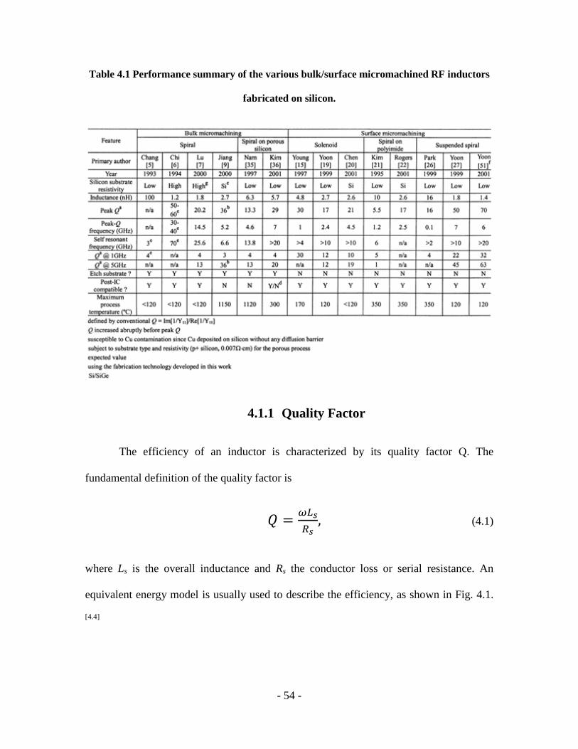
- 54 -
Table 4.1 Performance summary of the various bulk/surface micromachined RF inductors
fabricated on silicon.
4.1.1 Quality Factor
The efficiency of an inductor is characterized by its quality factor Q. The
fundamental definition of the quality factor is
=
, (4.1)
where Ls is the overall inductance and Rs the conductor loss or serial resistance. An
equivalent energy model is usually used to describe the efficiency, as shown in Fig. 4.1.
[4.4]

- 55 -
Fig. 4.1 Equivalent energy model representing the energy storage and loss mechanisms in a
monolithic inductor. Note that Co=Cp+Cs.
As a result, we have
= 2 | − |
= ×
+ [
+ 1] ⋅ × 1 −
− ,
(4.2)
where ωLs/Rs accounts for the magnetic energy stored and the ohmic loss in
the conductor. The second term stands for the loss factor due to the silicon
substrate. The last term is the self –resonance factor due to the increase in
the peak electric energy with frequency and the vanishing of Q at the self-
resonance frequency.

- 56 -
4.1.2 Self-resonance Frequency
The impedance of an inductor is a complex function of the frequency, which
consists of the real part (resistance) and the imaginary part (reactance). Because of the
parasitic capacitance between neighboring turns, the reactance of an inductor is
determined by the combined effect of the capacitance and the inductance. As frequency
increases, the reactance becomes zero at some frequency point, and remains negative
afterwards. This critical frequency value where the reactance is zero is defined as the
self-resonance frequency fSR. As shown in Fig. 4.2, the quality factor drops below zero
when the reactance of the inductor becomes capacitive.
Fig. 4.2 The quality factor as a function of frequency.

- 57 -
4.1.3 Different Types of Integrated Inductor
The discrete inductors are usually made by wrapped coils, and soldered onto PCB
board, while an on-chip integrated inductor is fabricated on Si substrate by IC micro-
fabrication technologies. For a magnetically enhanced on-chip inductor, the numbers of
coil and winding geometries have been investigated including spiral, toroidal, solenoid
and meander structures. [4.5]
Spiral Structure
One of the earlier applications of the spiral-type inductive components was
integrated magnetic recording heads, which have been investigated since the 1970s.
[4.6][4.7]
Figure 4.3 shows a top view and a side view of the spiral inductors. Figure 4.4
shows the equivalent circuit. The quality factor could be calculated as
(4.3)
A spiral inductor fabricated on top of a 90nm CMOS process is shown in Fig 4.5. [4.3] A
converter serving spiral structure based inductor was simulated to demonstrate a high
inductance of 1.2µH, which consists of copper windings sandwiched between two
laminated NiFe layers shielding the magnetic flux induced from the inductor windings.
[4. 8 ] A planar micromachined spiral inductor at low (Hz – kHz) frequencies with a
LCsubloss
electricpmagneticpff
R
L
E
EEQ ⋅⋅=
−⋅= .
0
0__2
ωπ

- 58 -
magnetic core was claimed to have an inductance of 2.2 µH/mm2, four to five times
greater than its air-core reference. [4.9]
Fig. 4.3 (a) Top view and (b) side view of a 3.5-turn square spiral inductor.
Fig. 4.4 The equivalent circuit of a spiral inductor.

- 59 -
Fig. 4.5 Optical microscope images of copper/polyimide based 4-turn elongated spiral
inductor with magnetic material fabricated in a 90 nm CMOS process.
The magnetically sandwiched spiral inductors suffer from high copper loss,
because the magnetic field generated by the top and bottom magnetic layers crosses the
coils. Due to the large air gap between the neighbor turns, the number of turns needs to
be very large in order to obtain high inductance, as a result, leading to large dimension.
However, it does have high bulk energy ( =
⋅ ⋅
) and does not have via
problems, which is brought in by the fabrication process.

- 60 -
Toroidal Structure
An integrated toroidal inductor is fabricated on a silicon wafer by using a
multilevel metallization technique to realize the coils, as shown in Fig. 4.6.[4.10] In one
reported toroidal structure, a wrapped coil was wound around a 30 µm thick micro-
machined NiFe bar, which can produce a closed magnetic circuit as well as minimized
leakage flux. A 4mm by 1mm by 130 µm dimension is able to achieve 0.4 to 0.1 µH at 1
kHz to 1 MHz.[4.11]
The drawbacks of toroidal inductors include the complexity of via process, the
high serial resistance, fast saturation, low bulk energy.
Fig. 4.6 3-D illustration of the on-chip integrated toroidal inductor. The circled section
represents a unit turn.

- 61 -
Meander Structure
A meander inductor is shown in Fig. 4.7. The three-dimensional meander
magnetic core (NiFe) is wrapped by the planner meander shape coil to form flux loop. An
inductance of 30 nH/mm2 was achieved at 5 MHz with 30 turns and a dimension of 4mm
by 1mm. [4.12] The quality factor of a meander inductor could be expressed as
=()
, (4.4)
Where Aw is the cross section area of conductor, 2(W+L) is the length of one meander
coil turn, and ρ is the resistivity of conductor material.
Fig. 4.7 Schematic diagrams of (a) the meander type integrated inductor with multilevel
magnetic core and (b) the more conventional solenoid-bar type inductor. The structure of
the two inductor schemes is analogous.

- 62 -
The meander inductor also has three layers. As a result, the via process of the
magnetic material adds to the complexity, which also introduces the parasitic air gaps.
Besides, it suffers from the low bulk energy, too. However, because of the single
electrical layer, it does not have high serial resistance problem.
Solenoid Structure
The electroplated solenoid integrated inductor has several advantages over its
counterparts. It is more compact because only the bottom conductor lines occupy areas on
the substrate. A relatively small increase in the area or number of turns leads to high
inductance. A typical layout is shown in Fig. 4.8.[4.13] An electrically tunable integrated
radio frequency inductor based on a planar solenoid with a thin-film NiFe core was
reported to achieve 85%, 35% and 20% at 0.1, 1 and 2 GHz, respectively, for inductances
in the range of 1 to 150 nH. [4.14] The calculation of an ideal solenoid inductor can be
written as
=
, (4.5)
where Ac is the cross-sectional area, lc is the length of the closed magnetic core. The
quality factor is
=
=
, (4.6)
where Aw is the cross-sectional area of the conductor, 2W is the length of the coil per turn
and r is the resistivity of the metal conductor.

- 63 -
Fig. 4.8 Schematic design of an integrated solenoid inductor: (a) top view and (b) cross-
section view.
4.1.4 The Magnetic Core
From the material point of view, the magnetic core materials need to exhibit low
coercivity, high magnetization, and low magnetic loss. The magnetic loss can be defined
as the ratio of the imaginary and real part of the permeability, = " ′⁄ . The
magnetic thin films are often patterned to reduce eddy current, and the shape-induced
magnetic anisotropy would also increase the resonance frequency. [4.15] [4.16] Other than
that, reducing the thickness of the films or using laminations are also able to increase the
resonance frequency of the inductors while reducing the magnetic loss. A 15% tuning
range and a quality factor between 5 and 11 up to 5 GHz were reported of an on-chip
inductor that used a NiFe film. The eddy currents and ferromagnetic resonance are
suppressed in the permalloy film using patterning and lamination in order to enable
operation in the RF range. [4.17]

- 64 -
From the fabrication point of view, the magnetic material should be fully
compatible with CMOS processing. As a result, they need to come with matured
deposition and etching techniques and high-temperature stability. To develop a technique
to prepare magnetic films that is fully compatible with standard CMOS technology
processing is challenging. Besides FeCoB, two commonly used soft magnetic materials
are Co-4.5%Ta4.0%Zr and Ni-20%Fe. They could be prepared using magnetron
sputtering deposition. Fig. 4.9 shows a cross-section view of an integrated inductor.[4.18]
Fig. 4.9 Cross sectional SEM image of inductors integrated on an 130 nm CMOS process
with 6 metal levels. Two levels of CoZrTa magnetic material were deposited around the
inductor wires using magnetic vias to complete the magnetic circuit.

- 65 -
4.2 Prototype and Layout Design
As discussed earlier, the solenoid type inductors have the advantages of
compactness and high magnetic energy density. In order to study the effect of the number
of turns and the magnetic core shape on the inductance and quality factor, three types of
inductors were designed, fabricated and tested.
Type I design is shown in Fig. 4.10. This is a very conventional structure, in
which coils are wrapped around a rectangular magnetic core. The picture on the right is
Fig. 4.10 Inductor design type I. Left top is a schematic top view, where the blue pads
indicate the vias. Left bottom is the 3-D schematic. The red rectangular on the top is the top
layer metal consisting the top layer of the coil, while the blue rectangular is the bottom layer.
The top and bottom metal are connected by vias, which are in green and yellow. The right
picture is the 6-layer layout design done with Cadence.

- 66 -
(a)
(b)
Fig. 4.11 The cross sectional view of inductor type I, shown in Fig. 4.10, along (a) the
transverse direction and (b) longitudinal direction. The yellow parts indicate the metal, the
dark blue parts are the magnetic cores and the light blue area is the polyimide. The grey
part stands for the Si substrates.
the 6-layer layout design of a 10-turn type I inductor for the mask fabrication, and it was
drawn with the Cadence layout tool. The big rectangular loop along the contour is
- 67 -
designed for the ground signal connection purpose during testing. It also serves as the
shield for each single device, so that the testing signal is not affect by the devices around
it. The cross sectional views are shown in Fig. 4.11.
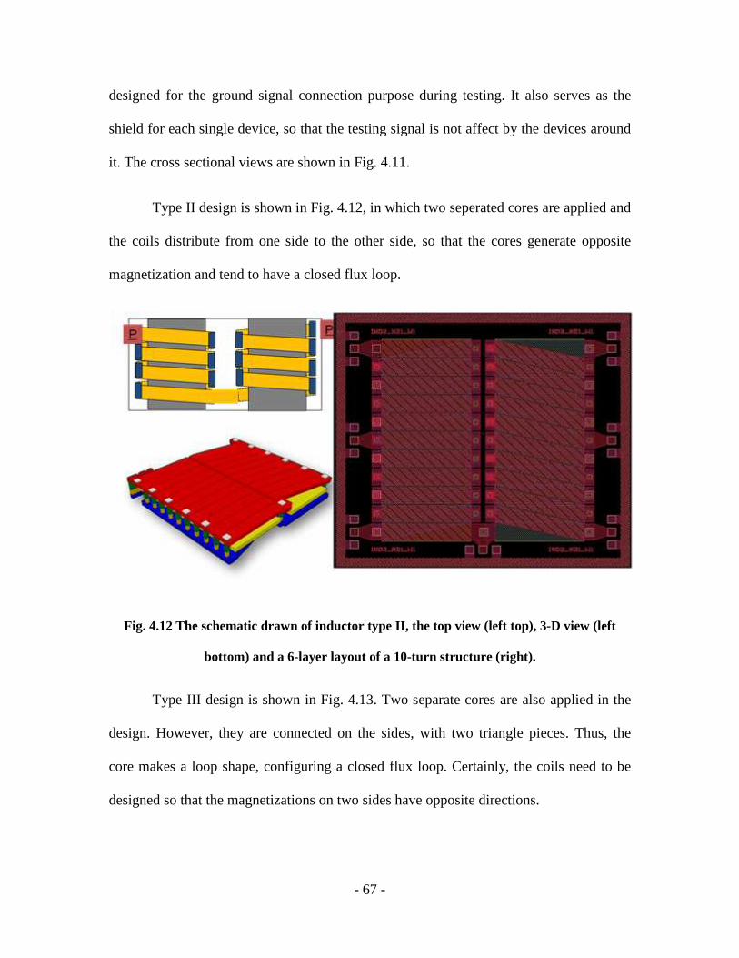
Type II design is shown in Fig. 4.12, in which two seperated cores are applied and
the coils distribute from one side to the other side, so that the cores generate opposite
magnetization and tend to have a closed flux loop.
Fig. 4.12 The schematic drawn of inductor type II, the top view (left top), 3-D view (left
bottom) and a 6-layer layout of a 10-turn structure (right).
Type III design is shown in Fig. 4.13. Two separate cores are also applied in the
design. However, they are connected on the sides, with two triangle pieces. Thus, the
core makes a loop shape, configuring a closed flux loop. Certainly, the coils need to be
designed so that the magnetizations on two sides have opposite directions.

- 68 -
Fig. 4.11 The schematic pictures of inductor type III, the top view (left top), 3-D view (left
bottom), and a 6-layer layout of a 10-turn device.
Five different numbers of turns were designed for each inductor type -- 6, 8, 10,
12, 14, respectively. Air core structures were also included into the layout, in order to
study the core effect. Parameters like the core dimensions, coil width and gaps are shown
in Table 4.2. The core dimension for Type I is 2 mm by 2.4 mm; That for Type II and III
is 1mm by 2.4mm for each side. Open structures, like the one shown in Fig. 4.14 are
especially designed for the testing purpose, which will be discussed in the following
sections. Some testing structures were designed on the layout to monitor the fabrication
quality, as shown in Fig. 4.15.

- 69 -
Fig. 2.14 The layout design of an 8-turn inductor Type I (upper) and its open structure with
only the contour ground structure and the testing pads (lower). The cross arrays in the open
area are the aligning marks.

- 70 -
Fig. 4.13 Layout design of the testing structures, including the via resistance testing bars,
polyimide step monitor, precision monitor and sheet resistance testing pads.

- 71 -
4.3 Theoretical Model
4.3.1 Inductance
The inductance of an inductor has two components, self Lself and mutual
inductance M.
L=Lself+M . (4.7)
Self Inductance
An alternating magnetic field can be induced when an alternating current is
flowing along a conductor, according to Ampere’s law. The self inductance of a
rectangular conductor is written as [4.19]
= 2 ⋅ ⋅ ⋅
+ 0.5 +⋅, (4.8)
where Lself denotes the conductor inductance in nH, l, w and t represent the length, width
and thickness of the conductor in cm, respectively.
By following equation 4.8, the self inductance of a rectangular conductor could be
calculated. Figure 4.16 shows the calculated results for 1 µm thick rectangular conductors
with different length and width. [4.20] The dimension of the conductor does have effects on
the self inductance, because the inductance is mainly determined by the outer magnetic
flux generated by the conductor. The inductance of a single loop in nanohenries is given
by [4.21]

- 72 -
Fig. 4.16 Self inductance value for a rectangular conductor versus its length and width (the
thickness is fixed at 1µµµµm).
= 4 ln − 2, (4.9)
where a is the radius and w is the width of the strip, both in centimeters.
The AC self inductance of a solenoid type inductor is given by [4.25]
() = ()
, (4.10)
where s the thickness of a single lamination of the core and δc is the skin depth of the
core, and

- 73 -
() = /, (4.11)
which is the DC self inductance, with N the number of turns, µc and lc the equivalent
permeability and length of the core, respectively.
Mutual Inductance
Mutual inductance M12 may be defined as the inductive influence of one coil or
circuit upon another, defined by
=
, (4.12)
where Ψis the flux generated by circuit 1, I1 is the current flows in circuit 1. The mutual
inductance in nanohenry between two parallel conductors is
= 2 ⋅ ⋅ , (4.13)
where l is the length of the conductor in centimeter and Q is a geometry coefficient,
defined by [4.22]
= ln !
+ 1 +
!−1 +
!
+ !, (4.14)
where GMD is approximately the average length of the conductors

- 74 -
One inductor could always be considered as two half parts. Each half has mutual
inductance with respect to the other half. The total mutual inductance is the sum of them
if they are connected in series along the same direction. Otherwise, the mutual inductance
due to the two halves tends to cancel each other. [4.23]
The AC mutual inductance of a solenoid type inductor was derived as [4.24]
() = ()
⋅
+ 2
⋅
,
(4.15)
where Rw(dc) is the AC winding resistance and A is a dimensionless quantity, which
depends on the winding conductor geometry. For a strip wire of width a and height b, the
quantity A is written as [4.25]
="#, (4.16)
where δ is the skin depth of the winding metal, p is the winding pitch or the distance
between the centers of two adjacent conductor lines.
The total AC inductance of a solenoid type inductor is Lac=Lself(ac)+M (ac).
4.3.2 Resistance and Skin Effect
The frequency dependence of the resistance of a conductor results from the non-
uniform distribution of the current density through the cross section. As the frequency

- 75 -
increases from DC to higher range, the current density tends to be higher near the skin,
which is so called skin effect. Eddy current could be generated when a conductor is
placed in an alternating magnetic field. According to Lenz’s law, conductors tend to
generate eddy current in order to resist the external magnetic field. The effective
distribution depth of the current from the skin, defined as skin depth or depth of
penetration, could be written as
=
$%, (4.17)
where f is the frequency, is the permeability of the core material, is the conductivity
of the conductor. Generally, the skin depth decreases as the frequency increases, and the
resistance increases accordingly. The resistance due to the skin effect is
=⋅
⋅(& ⁄ ), (4.18)
where ρ and l represent the resistivity and length of the conductor.
The AC winding resistance of a solenoid type inductor was derived to be
[4.26][4.27][4.28]
= () ⋅ [ & '()*+
&,-'*++ 2
&
⋅ & '()*+
&,-'*+],
(4.19)

- 76 -
where A is a dimensionless quantity, which depends on the winding conductor geometry.
The first and second terms in equation 4.15 represent the skin effect and the proximity
effect contributions to the winding AC resistance, respectively.
4.3.3 Lamination Core Loss
For a given magnetic material and frequency, the skin depth of the core can be
calculated with equation 4.13, and the effective resistance Re from eddy current loss can
be approximated as [4.29]
≈
. for
< 0.5, (4.20)
where L0 is the DC inductance, and t is the thickness of the lamination. The skin depth of
the FeCoB at 45 MHz is around 1.1 µm, calculated by equation 4.13. Generally, 1.1 µm
thick laminations should be sufficient to prevent the substantial eddy current losses in the
20 MHz to 50 MHz range. However, from equation 4.14, the effective resistance is
proportional to the square of the lamination thickness when it is smaller than 550 nm.
Hence, the loss can be significantly reduced by further reducing the lamination thickness.
[4.30]
The equivalent AC resistance of the core inside a solenoid type inductor is given
by [4.25]
= ()
&
, (4.21)

- 77 -
The total AC resistance Rac of an integrated inductor is the sum of the winding resistance
Rw and core equivalent series resistance Rc, Rac=Rw+Rc.
4.3.4 Parasitic Effects
Substrate Parasitics
The electromagnetic field generated by the on-chip integrated inductors interfaces
with the Si substrate, and induces substrate parasitic loss. For the solenoid type integrated
inductors, the substrate parasitic capacitor is formed between the bottom coils and the Si
substrate, with the dialectical layer in between.
Parasitic Capacitance between Lines
The parasitic capacitance also exists between each neighboring coil lines, both on
the top layer and bottom layer. The capacitance between two top conductor lines Ct and
that between two bottom lines Cb are described as [4.31]
= " = /=/(⋅")
, (4.22)
where ε is the dielectric constant of air, b is the thickness and w is the length of the
conductor line.
4.3.5 Quality Factor of the Solenoid type Inductors
An inductor could be equivalent to a circuit, shown in Fig. 4.17. The equivalent series
resistance Rs and reactance Xs are [4.27]

- 78 -
= (&0)(0)
, (4.23)
= (&0&
)
(&0)(0). (4.24)
Fig. 4.17 Equivalent circuit of an integrated inductor.
Hence, the equivalent series inductance Ls is =
. The quality factor could be
=1
. (4.25)
4.4 On-chip Fabrication
Step 1: PI1 formation
Polyimide layer-1 formation on the silicon substrate, shown in Fig.4.18. The
adhesion promoter VM-652 was pre-coated on the silicon surface. The polyimide PI2611
was spin coated with a Laurel WS-400 Lite series spin processor. Because the polyimide
is usually very thick, a multi-step spin speed is usually used to form a uniform coating.
The 3-step spin speeds were set to be 500 rpm for 30 seconds, 1000 rpm for 10 seconds

- 79 -
and 2000 rpm for 30 seconds. 20 minutes of softbake on the hot plate was taken
Fig. 4.18 A 10µµµµm thick polyimide layer was coated on the Si substrate.
afterwards at 150o. The curing process of PI2600 was performed in a nitrogen gas
flowing furnace tube. A slow heating up process is very important, so that the polyimide
surface does not crack. The cured polyimide layer was measured to be 10 µm.
Step 2: Deposit bottom coil seedlayer
A seedlayer of the bottom metal was deposited with PVD, shown in Fig.4.19. The
seedlayer consists of a 20nm Cr layer followed by a 100nm Cu layer. The Cr layer is able
to improve the adhesion between the Cu and polyimide surfaces.
Fig. 4.19 A seedlayer was deposited with PVD, for the bottom metal.
Step 3: Photo bottom coil
A thick layer of photoresist AZ P4620 was spin coated and patterned above the
seedlayer, as shown in Fig.4.20. The exposure time is 60 seconds, and the developing
took 2 minutes with the diluted developer AZ400K (1:4 DI water).

- 80 -
Fig. 4.20 A thick photoresist layer was patterned above the seedlayer.
Step 4: Electrical plating of the bottom coil
A commercialized electrolyte was used for the electrical plating process. The
current density was set to be 0.14 mA/mm2. The coil thickness was measured with the
Dektek profilometer, which was around 6 µm. Acetone was then applied on the wafer to
strip the photoresist layer. This step is shown in Fig.4.21.
Fig. 4.21 Electric plating of the bottom coils and the removal of PR.

- 81 -
Step 5: Etch coil seedlayer
The wet etching of the seedlayer requires two different solutions. In order to
remove the Cu seedlayer on the top, the diluted Ammonium hydroxide with a drop of
hydrogen peroxide (50:1:300 DI water) was used. To remove the Cr seedlayer, an
alkaline solution was made, so that the Cu layer was not affected. This alkaline solution
had 3 units of potassium ferricynide, 2 units of sodium hydroxide and 100 units of DI
water. After the removal of the seedlayer, the wafer looks like that shown in Fig.4.22.
Fig. 4.22 The schematic view of the wafer (upper) and a zoom-in picture of the real wafer
(lower) after the Cr/Cu seedlayer removed.
Step 6: Polymide layer-2 patterning
A second layer of polyimide (PI4100) was spin coated and patterned above the
bottom coil to form a 10µm thick dielectric layer, as shown in Fig.4.23. A lithography

- 82 -
process was performed in order to open the via openings. Because of the thickness of the
polyimide, the developing process might need to be repeated for two to three times.
Fig. 4.23 Polyimide layer-2 coating and patterning.
Step 7: PR patterning for magnetic core
As discussed in Chapter 3, the multilayer structure of FeCoB/Al2O3 serves as a
good magnetic core with high permeability and low loss. Due to the difficulty of the wet
etching of this multilayer structure, a lift-off patterning method was used for the magnetic
core. As a result, a thick photoresist layer was spin coated and patterned above PI2 layer,
as shown in Fig.4.24.
Fig. 4.24 Photoresist layer coating and patterning for the magnetic lift-off process.

- 83 -
Step 8: Magnetic deposition and lift- off
According the study in Chapter 3, the critical thickness of Al2O3 is 6 nm, above
which the anti-ferromagnetic coupling disappears. A 4 µm thick multi-layer was
deposited with PVD, which is almost the limit of the PVD deposition. The film starts to
peel off above this thickness due to the high induced stress. The composition of the core
is Cr (20nm) / [FeCoB (500nm)+Al2O3 (6nm)] × 8. The lift-off was done with acetone
and ultrasound applied. This step and the zoom-in pictures on the wafer are shown in
Fig.4.25.
Fig. 4.25 Schematic view of the lift-off process (upper), and pictures of the lift-off patterned
cores (lower).

- 84 -
Step 9: PI3 coating and patterning
A 10 µm layer of polyimide HD 4100 was coated and pattern above the magnetic
layer. Thus, a dielectric layer was formed underneath the top metal layer, while leaving
the vias openings, as shown in Fig.4.26.
Fig. 4.26 Polyimide layer-3 was spin coated above the magnetic layer, and patterned to have
the via openings.
Step 10: Deposit top coil seedlayer
Similar with step 2, the seedlayer of top metal was deposited with PVD, as shown
in Fig. 4.27(a). The only difference was that a low power re-sputtering step was taken
after the regular Cu deposition. This process could make a continuous seedlayer formed
on the side wall of the via openings. The N2 plasma hit on the Cu atoms at the via bottom,
which then get reflected and re-deposited on the side wall, as shown in Fig. 4.27(b).

- 85 -
(a)
(b)
Fig. 4.27 (a) A seedlayer (Cr/Cu) was deposited above PI3 layer. (b) The re-sputter process
is able to re-distribute the seedlayer in the via openings during the deposition.
Step 11: Photo top metal
In this step two different masks were used to pattern the thick photoresis. Because
the via openings are around 30µm deep and 30 µm to 50 µm wide, the high aspect ratio
added to the difficulty of cleaning the photoresist inside the openings. As a result, one
mask that only patterns the via openings were used for lithography before applying the
top coil mask. Thus, photoresist inside the via openings was exposed for a longer time an
d pre-developed before the coil structure got exposed. This step is shown in Fig.4.28.
Step 12: Plate top coil and etch top coil seedlayer
This step is exactly the same with the electrical plating and seedlayer removing
process of the bottom coil, as shown in Fig.4.29. Some pictures of the fabricated devices
are shown in Fig.4.30.
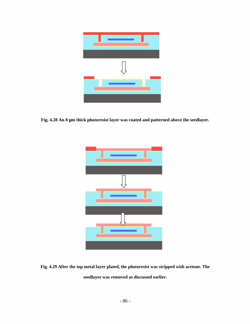
- 86 -
Fig. 4.28 An 8 µµµµm thick photoresist layer was coated and patterned above the seedlayer.
Fig. 4.29 After the top metal layer plated, the photoresist was stripped with acetone. The
seedlayer was removed as discussed earlier.

- 87 -
Fig. 4.30 Picture of the on-chip inductors, Type I, type II and Type III respectively.
- 88 -
4.5 On Wafer Measuring
The testing frequency range of the inductors located between 300 kHz and 500
MHz. At the high frequency range, the signal wavelength is comparable with the
dimension of the IC component. As a result, the current and voltage do not remain
unchanged everywhere on the chip and they need to be treated as propagating
microwaves. The characterization of the on-chip integrated inductors requires the
microwave testing system.
4.5.1 Testing Platform
The testing system used in the work consists of a vector network analyzer, a probe
station, and two RF GSG probes. The parasitic effects induced by the connection cables
could be minimized with this on-chip testing method.
Vector network analyzer
The vector network analyzer performs measurements based on the reflection
method. The measured scattering matrix (S- parameters) provides a complete description
of the networks. It relates the voltage waves incident on the ports to those reflected from
the ports. Once the scattering parameters of the network are know, conversion to other
matrix parameters can be performed if necessary. The scattering matrix is defined as
&& = , (4.26)

- 89 -
where Vn- represents the amplitude of the voltage wave reflected from port n and Vn
+
represents the amplitude of the one incident on port n. A specific element the scattering
matrix can be determined as
2 = 3
3 |3
4.6782. (4.27)
Probes and probe stations
The RF probes perform the physical contact to the device under test, as shown in
Fig. 4.31(a). In order to control the position of the probe tips, they are mounted on to a
probe station by screwed on to the arms of two micropositioners, as shown in Fig.4.31 (b).
(a) (b)
Fig. 4.31 (a) The GSG probes are mounted on the arms of two micropositioners which can
be controlled by the (b) probe station. Meanwhile, they are connected to the two ports of the
vector network analyzer through the low loss coaxial cables.

- 90 -
The station enables a high accuracy alignment as well as a tight control of the pressure
applied to the probes. Meanwhile, the GSG probes are connected to the two port of the
network analyzer through the low loss coaxial cables, also shown in Fig. 4.13(a).
4.5.2 Calibration
The commercialized on-chip calibration substrate was used in order to calibrate
the VNA directly at the probe tip interface. Different calibration sets could be used, such
as SOLT (Short-Open-Load-Through), LRL (Line-Reflection-Line), and LRM (Line-
Reflection-Match). The SOLT calibration method was applied in this work.
SOLT calibration
The SOLT calibration procedure goes through a few steps.
Step 1: Select the Right Option on the VNA
Select the two-port calibration option under the calibration menu of the VNA.
Step 2: Measuring the Short Standard
This step is shown on the left top of Fig. 4.32. After the probe tips touching the
pad of the standard, simply click the “short” soft button on the screen, confirming the
executing of the short calibration.
Step 3~5: Measuring the Open and Load Standard
Similar with step 2, these steps are done by contacting the probe tips to the
standards and confirming it in the VNA.

- 91 -
Fig. 4.32 The SOLT calibration procedure includes four steps: Measuring the short, open,
load and through standard.
After the calibration, the testing system is ready to be used for on-chip inductor testing.

- 92 -
4.5.3 Parameter Extraction
In order to extract the scattering parameters got form the VNA, an equivalent
circuit model needs to be set up. There are three possible setups for measuring an
inductor with a VNA, as shown in Fig. 4.33. [4.20]
Fig. 4.33 Three possible configurations for measuring a two-port device ZL with a VNA.
They are two-port measurement with the device placed in series with the ports, two-port
measurement with the device placed in parallel with the ports, and one-port measurement,
respectively from left to right.
ΠΠΠΠ Model of Two-port Measurement with the Device Placed in Series
The Π model shown in Fig. 4.34 is the electric circuit most often used to calculate
the scattering parameters of a two-port measurement of integrated inductors for RF
application.

- 93 -
Fig. 4.34 Setup for the calculation of the scattering parameters of a two-port measurement
with the ΠΠΠΠ model.
De-embedding Technique
Because the probe tips are not able to be built small enough to directly contact the
on-chip device, the contact pads are usually designed to fit the probe tip dimensions, as
shown in Fig. 4.14. In order to eliminate the parasitic impedance that brought by the
testing pads, the de-embedding technique was developed.
First, the complex scattering parameters got with the device under testing (DUT)
need to be converted into the admittance matrix [Y], using the following equations:
= 9
*&:+*:+::*:+*:+&::
, (4.28)

- 94 -
= 9
&:*:+*:+&::
, (4.29)
= 9
&:*:+*:+&::
, (4.30)
= 9
*:+*&:+::*:+*:+&::
, (4.31)
where Z0 is 50 Ohm. Second, measure the S parameters of the open structure with only
the testing pads but not the DUT, as shown in the lower picture of Fig. 4.14. Thus, the
accurate admittance matrix is
[Yde-embed]= [YDUT]-[YPAD]. (4.32)
The de-embedded S-parameters could be calculated by
= *;&;+*;;+;;*;;+*;;+&;;
, (4.33)
= &;;*;;+*;;+&;;
, (4.34)
= &;;*;;+*;;+&;;
, (4.35)
= *;;+*;&;+;;*;;+*;;+&;;
, (4.36)
where Y0=1/Z0.

- 95 -
Inductor Parameters
The inductance, resistance and quality factor of the inductor could be calculated
with the de-embedded admittance matrix, as the following
=⋅ !" &
;, (4.37)
= #(&;
), (4.38)
= −<(;) (;)
. (4.39)
4.6 Result and Analysis
Measurement was done on 25 sets of on-chip integrated inductors. The
dimensions are shown in Table 4.2. As the number of turns gets increased, the width of
coil decreases in order to maintain a constant value of the gap. After the on-chip testing
with the testing platform discussed earlier, the de-embedding was done and the measured
inductance and quality factors were extracted from the admittance parameters. These
results were plotted and going to be discussed in this section.

- 96 -
Table 4.2 The Design Matrix of the on-Chip Integrated Inductors
# of turns on single core
width of single
magnetic core
length of single
magnetic film
width of Cu wire
gap between each two Cu
wire turns
N Wm(um) Lm(um) W(um) gap(um)
Type I (including air-core structure)
6 2000 2400 322 20
8 2000 2400 246 20
10 2000 2400 198 20
12 2000 2400 164 20
14 2000 2400 140 20
Type II&III (including air-core structure)
6 1000 2400 322 20
8 1000 2400 246 20
10 1000 2400 198 20
12 1000 2400 164 20
14 1000 2400 140 20

- 97 -
4.6.1 Number-of-Turn Dependency
Figure 4.35 ~ 4.37 show the frequency dependence of inductance and quality
factor for three different designs, with five different numbers of turns, from 6 to 14. For
inductors of Type I, as the number of turns N increases, the inductance value was
measured to range from 13 nH to 53 nH, around 35MHz. It can be seen that the
inductance is proportional to N2, as described in equation (4.5). The inductance of Type II
increases from 14 nH to 57 nH as N increases and that of Type III ranges from 15 nH to
60 nH. It could be concluded that the design of Type III generally provides the highest
inductance, with the indistinct advantage.
Inductors with lower number of turns show higher quality factors, and it is related
to the lower resistance loss and lower winding capacitance. The measured peak quality
factor of Type I is around 8 for 6 turns of winding; the peak quality factor of Type II is
6.7 and that of Type III is 6.3. At low frequencies, the quality factor of each type is very
close for different N values, which indicates that the N dependency of the quality factor is
not very obvious at frequency range much lower than the peak region. As frequency goes
up, the quality factor curves start to spread, indicating the high frequency loss of the
inductors, resulting from the core and parasitic effects.
Certainly, by magnetically annealing the cores at high temperature, the magnetic
property could be dramatically improved, and so does the inductance and quality factor.

- 98 -
Fig. 4.35 The measured inductance and quality factor of inductor type I, for different
numbers of turns.

- 99 -
Fig. 4.36 The measured inductance and quality factor of inductor type II, for different
numbers of turns.

- 100 -
Fig. 4.37 The measured inductance and quality factor of inductor type III, for different
numbers of turns.

- 101 -
4.6.2 Core Structure Dependency
For a solenoid type inductor with the magnetic core of 2mm ×2.4mm in area, the
inductance is close when the number of turns is the same for the three types of cores,
shown in Fig. 4.38. Type III does not show a very obvious advantage on it. The only
difference between Type II and Type II is the connection between the two-sided magnetic
bars. Theoretically, Type III with a closed core loop tends to keep the magnetic flux
inside the magnetic material, generating less leakage. However, the magnetic material
was not annealed before performing this measurement. The magnetic domains inside the
magnetic material are very likely with disordered magnetization directions. Compared
with the rectangular cores, the triangle shape magnetic pieces connecting the two-sided
bars do not have a high permeability, due to the lower shape anisotropy. Hence, they do
little effect on keeping a condensed magnetic loop. This lousy magnetic property could
be improved by doing the magnetic high temperature annealing of the devices. However,
the above discussion about the shape anisotropy does explain the fact that the Type I
inductor shows lower inductance than Type II and III. The rectangular core of Type I has
a lower length to width ratio (2.4/2) than that of Type II and III (2.4/1), which means a
smaller shape anisotropy, thus a lower permeability along the axial direction. As a result,
for a fixed number of turns, inductor Type I shows lower inductance than the other two
types.
The comparison of the inductance between the magnetic core and air core devices
can be seen very clearly from each plot of Fig. 4.38. As the number of turns increases, the
inductance of Type I is increased with a magnetic core by a factor of 3 ~ 6.75, compared

- 102 -
with that of an air core structure. The inductance of Type II and III is increased by a
factor of 3.75 ~ 6.35.
(b)
(a)

- 103 -
(c)
(d)

- 104 -
Fig. 4.38 The inductance plots for different core types, with the same numbers of turns. (a)
N=6; (b) N=8: (c) N=10 (d) N=12; (e) N=14.
The effect of the magnetic core on the quality factor could be seen from Fig. 4.39.
Inductor Type I with a magnetic core of shows higher quality factor for cases of N=6, 8,
10, 12, respectively, but the advantage gets eliminated as the number of turns increases. It
even gets lower than that of Type III with a magnetic core when N equals 14. Hence, the
magnetic core in Type I design tends to have higher loss for large number of turns. It
could be related to the eddy current that is generated inside the core due to the alternative
magnetic field. For a certain type of magnetic material, a larger cross section usually
shows higher eddy current induced loss, as discussed in Chapter 3.
(e)

- 105 -
The loss generated purely from the winding coil and the substrate could be seen
from the quality factor plots of the air core inductors. The inductors of Type I design
have a much higher quality factor over the other two types without the magnetic core.
Although the total area, the wire width and gap are the same for the same number of turns,
the two-sided solenoid structure for Type II and III has a double winding turns, leading to
higher electrical loss.
(a)

- 106 -
(b)
(c)

- 107 -
Fig. 4.39 The quality factor plots for different core types, with the same numbers of turns.
(a) N=6; (b) N=8: (c) N=10 (d) N=12; (e) N=14.
(d)
(e)

- 108 -
4.6.3 Conclusion
For a solenoid type inductor, the performance could be optimized by improving
the core structure and adding winding turns. Add more winding turns is the most straight
forward way of increasing the inductance. However, the thinner conductor line dimension
would probably add to the difficulty of fabrication process. By dividing the magnetic core
into halves and winding the coils on two sides and in series, the inductance could be
increased. Joining the separated halves at two ends is able to improve the inductance
further due to a closed magnetic loop inside the core material.
The influence on the quality factor was also discussed. The loss comes from the
magnetic core, the inductor winding and the substrate. For large number of turns, the
two-sided magnetic core shows lower loss than the single piece design, due to the
reduced eddy current loss.
Moreover, a magnetic annealing is very likely able to improve the magnetic
properties of the magnetic core, hence, reducing the overall loss.

- 109 -
REFERENCES
4.1 C. H. Ahn and M. G. Allen, “A Planar Micromachined Spiral Inductor for Integrated
Magnetic Microactuator Applications”, J. Micromech. Microeng. 3, 37-44 (1993).
4.2 V. K. Varadan, K. J. Vinoy and K. A. Jose, “RF MEMS and Their Applications”,
(John Wiley & Sons, Ltd.), 2003.
4.3 J. B. Yoon, B. Kim, Y. S. Choi, and E. Yoon, “3-D Construction of Monolithic Passive
Components for RF and Microwave ICs Using Thick-metal Surface Micromachining
Technology”, IEEE Transactions on Microwave Theory and Techniques, VOL., 51, NO.
1 (2003).
4.4 http://holst.stanford.edu/~CPYue
4.5 D. S. Gardner, G. Schrom, F. Paillet, B. Jamieson, T. Karnik and S. Borkar, “Review
of On-Chip Inductor Structures With Magnetic Films”, IEEE Trans. Mag., VOL. 45, NO.
10 (2009).
4.6 B. Wagner, M. Kreutzer and W. Benecke, “Linear and rotational magnetic
micromotors fabricated using silicon technology”, Proc. IEEE Micro. Electro. Mech. Sys.
Workshop, pp 183-9, (1992).
4.7 K. Yanagisawa, A. Tago, T. Ohkubo and H. Kuwano, “Magnetic Microactuator”, 4th
IEEE Workshop on Micro Electro Mech. Sys., pp 120-4, (1991).
4.8 J. M. Boggetto, Y. Lembeye, J. P. Ferrieux, Y. Avenas, “Micro Fabricated Power
Inductors on Silicon”, IEEE Power Electronics Specialist Conference, pesc 02, (2002).
4.9 C. H. Ahn and M. G. Allen, “A Planar Micromachined Spiral Inductor for Integrated
Magnetic Microactuator Applications”, J. Micromech, Microeng., 3, 37-44 (1993).

- 110 -
4.10 W. Y. Liu, J. Suryanarayanan, J. Nath, S. Mohammadi, L. P. B. Katehi, and M. B.
Steer, “Toroidal Inductors for Radio-frequency Integrated Circuits”, IEEE Trans.
Microwave Theory and Techniques, VOL. 52, NO. 2 (2004).
4.11 C. H. Ahn, Y. J. Kim and M. G. Allen, “A Fully Integrated Planar Toroidal Inductor
with a Micromachined Nickel-Iron Magnetic Bar”, IEEE Trans. Components, Packaging,
and Manufacturing Technology – Part A, VOL. 17, NO. 3 (1994).
4.12 C. H. Ahn, and M. G. Allen, “A New Toroidal-meander Type Integrated Inductor
with a Multilevel Meander Magnetic Core”, IEEE Trans. Magnetic, VOL. 30, NO. 1
(1994).
4.13 D. W. Lee, K. P. Hwang, and S. X. Wang, “Fabrication and Analysis of High-
performance Integrated Solenoid Inductor with Magnetic Core”, IEEE Trans. Magnetic,
VOL. 44, NO. 11 (2008).
4.14 M. Vrouble, Y. Zhuang, B. Rejaei, and J. N. Burghartz, “Integrated Tunable Magnetic
RF Inductor”, IEEE Electron Device Letters, VOL. 25, NO. 12 (2004).
4.15 D. S. Gardner, G. Schrom, P. Hazucha, F. Paillet, T. Karnik, S. Borkar, J. Saulters, J.
Owens, and J.Wetzel, “Integrated on-chip Inductors with Magnetic Films,” Int. Electron
Devices Meeting, pp. 1–4 (2006).
4.16 Y. Zhuang, M. Vroubel, B. Rejaei, J. N. Burghartz, and K. Attenborough, “Shape-
induced Ultrahigh Magnetic Anisotropy and Ferromagnetic Resonance Frequency of
Micropatterned Thin Permalloy Films,” J.Appl. Phys., VOL. 99, pp. 08C705–3 (2006).
4.17 J. Salvia, J. Bain, and C. P. Yue, “Tunable on-chip Inductors up to 5 GHz Using
Patterned Permalloy Laminations”, IEEE International Electron Devices Meeting, IEDM
Technical Digest, pp. 943 – 946, (2005).

- 111 -
4.18 D. S. Gardner, G. Schrom, P. Hazucha, F. Paillet, T. Karnik, S. Borkar, “Integrated
on-chip Inductors with Magnetic Films”, International Electron Device Meeting, 8P5,
(2006).
4.19 F. W. Grover, “Inductance Calculations”, Dover Publications, Inc., (2004).
4.20 J. Aguilera and R. Berenguer, “Design and Test of Integrated Inductors for RF
Applications”, Kluwer Academic Publishers, (2003).
4.21 L. Bahl and P. Bhartia, “Microwave Solid State Circuit Design”, John Wiley & Sons,
New York, (1988).
4.22 A. L. L. Pun, “On-chip Planar Spiral Inductor Induced Substrate Effects on Radio
Frequency Integrated Circuits in CMOS Technology”, The Hong Kong University of
Science & Technology, Ph. D work, (1998).
4.23 M. Brooks, H. M. Turner, “Inductance of Coils”, University of Illinois Bulletin,
(1912).
4.24 M. K. Kazimierczuk, G. Sancineto, G. Grandi, U. Reggiani, and A. Massarini, “High-
Frequency Small-Signal Model of Ferrite Core Inductors,” IEEE Trans. Magn., VOL. 35,
pp. 4185–4191 (1999).
4.25 G. Grandi, M. K. Kazimierczuk, A. Massarini, U. Reggiani, and G. Sancineto, “Model
of Laminated Iron-Core Inductors for High Frequencies,” IEEE Transactions on
Magnetics, VOL. 40, NO. 4 (2004).
4.26 P. J. Dowell, “Effects of Eddy Currents in Transformer Windings,” Proc. Inst. Elect.
Eng., VOL. 113, pp. 1387-1394 (1996).

- 112 -
4.27 M. Bartoli, A. Reatti, and M. K. Kazimierczuk, “High-Frequency Models of Ferrite
Core Inductors,” in Proc. IEEE Int. Conf. Industrial Electronics,Control, Instrumentation,
and Automation (IECON’94), Bologna, Italy, Sept. 5–9, pp. 1670–1675, (1994).
4.28 M. Bartoli, A. Reatti, M. K. Kazimierczuk, “Modeling Iron-Powder Inductors at
High-Frequencies,” in Proc. IEEE Industry Applications Soc. Annu. Meeting, Denver,
CO, Oct. 2–7, pp. 1225–1232 (1994).
4.29 J. Lammeraner and M. Stafl, “Eddy Current”, Lodon, U. K.: Iliffe (1966).
4.30 J. W. Park and M. G. Allen, “Ultralow-Profile Micromachined Power Inductors with
Highly Laminated Ni/Fe Cores: Application to Low-Megahertz DC-DC Converters”,
IEEE Transactions on Magnetic, VOL. 39, NO. 5 (2003).
4.31 Y. J. Kim and M. G. Allen, “Surface Micromachined Solenoid Inductors for High
Frequency Applications”, IEEE Transactions on Components, Packaging, and
Manufacturing Technology-Part C, VOL. 21, NO. 1 (1998).

- 113 -
5 Soft Magnetic Material Applied
Vibration Energy Harvesting
5.1 Introduction
Recent years, the application of mobile electronics and wireless sensors have been
developing rapidly in several fields, including environmental, industrial and medical. The
traditional power supply system, including batteries and wired sources, are suffering from
several drawbacks. Batteries need frequent recharging or replacement, which is costly
and impossible especially for the wireless networks with thousands of physically
embedded nodes [5.1]. And the power supply cable seriously limits the flexibility. As a
result, self-renewable power supply is becoming a critical issue in the applications of
mobile electronics and wireless sensors.
Energy harvesting, sometimes defined as “power scavenging” or “energy
extraction”, is the way to convert the ambient to usable electrical energy. The critical part
might be smart materials or structures. And the collected energy is generally to drive the
wireless electric devices or charge the embedded batteries.

- 114 -
5.1.1 Available Energy Sources
There are different types of available ambient energy, such as solar, wind,
vibration, thermal and RF wave, etc. Table 5.1shows most of the available ambient
energy sources and their performance. [5.2]
Table 5.1 Comparison of different types of available ambient energy sources and their performance
Solar Energy
Solar energy is the most well known and widely applied source, since the solar
cells are able to generate excellent power density with high efficiency. During peak hours,
the power density of solar radiation on the Earth’s surface is approximately
100mW/cm2.[5.3] And the silicon solar cells are a relatively mature technology with
efficiencies ranging from 12% to 25%. However, the advantage could be easily limited
when no sunlight present because the device is deeply embedded or when the panel is
obscured by rain, dirt or snow.

- 115 -
Vibration Energy
Vibration energy harvesting has great potential simply because the vibration
energy source is easily accessible. The available vibrating source is almost everywhere
from vibrating equipment, machinery and structures like bridge, working microwave,
running automobile, aircraft wing, etc. Hence, the vibration energy might be the most
available energy source for the wireless sensors compared with the other choices. The
current technology is focusing on conversion of the vibration energy from the vibrating
surface into electric energy. And the output power could be as high as 63 mW from a
device with a total volume of 75cm3. Vibration energy harvesting is not only able to
provide high output electric power with high efficiency, but also reduce the unnecessary
noise or mechanical vibration which might potentially cause structure damage.
Thermal Energy
Power generation based on thermoelectric effects has been known since the
Seebeck effect was discovered in the 1800s.[5.4] The Seebeck effect is defined as, a
temperature difference across a conductor generates an electrical potential. It converts
thermal energy into electrical energy. Figure 5.1 illuminates the power generation mode
of thermoelectric material[5.5].

- 116 -
Fig. 5.1 Power-generation mode of thermoelectric material.
Generally, a number of thermoelectric elements can be connected electrically in
parallel and/or in series shaping a thermoelectric generator (TEG) device.[5.6] Identifying
materials with a high thermoelectric figure of merit Z(=S2σ/k) has been proven an
extremely challenging task. The solid state energy calls for materials with high electrical
conductivity σ, high Seebeck coefficient S and low thermal conductivity k.[5.7]
Development of new concepts and theories about electron and phonon transport speeded
up the research on thermoelectric material after 30 years of slow progress. The Z value of
AgPbmSbTe2+m is over 1.5 around 700K. Figure 5.2 shows the figure of merit ZT as a
function of temperature for several bulk thermoelectric materials [5.5].

- 117 -
Fig. 5.2 Figure of merit ZT as a function of temperature for several bulk thermoelectric materials.
RF Energy
Radio frequency (RF) radiation has been applied in the information exchange of
ID and credit cards. It seems like only very small amount of electromagnetic radiation
energy was involved in this process. However, most of the electrical equipments,
including the cell phones, GPS, broadcast radio, TV and microwave ovens, are generating
the RF energy everywhere all the time, which makes the RF energy a very ample and
accessible source. The problem is collecting all these disparate sources and converting
them in useful energy. The conversion is based on a rectifying antenna (rectenna),
constructed with a Schottky diode located between the antenna dipoles.[5.8] It was

- 118 -
reported that 2.5mW power from X-band source horn antenna with 1W 10GHz radiation
to a receiver horn antenna for driving piezo-sensor nodes over a distance of 0.61m.[5.9]
However, the energy provided by the RF energy generator is still very low and with a low
efficiency.

- 119 -
5.1.2 Vibration Energy Harvesting Mechanisms
Table 5.2 Comparison of several key figures of merit for different vibrating energy
harvesting mechanisms
Mechanisms/Products fcenter
(Hz)
a
(g)
Pmax
(mW)
Routput
(Ω)
Vtotal
(cm3)
Power
Density
(mW/cm3)
HPBW*
(Hz)
Magnetoelectric micro-
cantilever[5.10] 52 0.06 0.046 4k 0.15 0.31 0.5
Electrostatic[5.11] 50 0.91 1.052 - 1.8 0.58 -
Magnetoelectric composite
beam[5.12] 40 1 - 3M - 0.4 -
Volture Piezo Energy
Harvester-V25W[5.13] 30 1.1 6.5 - 0.98 6.63 -
Magnetoelectric sensor
based system[5.14] 60 0.1 10.8 - 113 0.096 2.1
Magnetostrictive
cantilever[5.15] 58.1 1 0.2 ~80 - - -
Perpetuum PMG37[5.16] 21.9 1 92 - 130.67 0.7 12.9
KCF technologies
VPH300[5.17] 360 0.239 4.1 - 208.86 0.0196 5
This work: High-µ beam
with bias fields 54 0.57 74 1 68.96 1.07 10
*Power density, in unit of mW/g cm3.

- 120 -
There are three main transduction mechanisms employed to harvest vibration
energy. They are electromagnetic (inductive), piezoelectric and electrostatic
(capacitive).[5.18] Table 2 shows the comparison of several key figures of merit for
different vibrating energy harvesting mechanisms.
Piezoelectric generators
The piezoelectric effect was discovered in 1880. If certain crystals were subjected
to mechanical strain, they became electrically polarized and the degree of polarization
was proportional to the applied strain. Conversely, these materials deform when exposed
to an electric field. [5.18] Moreover, this effect is anisotropic. The piezoelectric generators
converts the vibration induced deforming in the piezoelectric material into electrical
energy.
The first US patent on energy harvesting was issued to a piezoelectric generator
whose output was rectified and stored into a capacitor. [5.19] Studies have shown that an
average gait walking human of weight 68kg, produces 67 W of energy at the heel of the
shoe[5.20]. A shoe heel mounted piezoelectric energy harvester was claimed to generate an
average power of 8mW. [5.21] The cantilever model based structure is used to harvest the
vibration energy at a particular frequency by forming a resonator, since the resonator
absorbs the maximum energy from the source when the system reaches sympathetic
vibration. An electromagnetic micro-cantilever device with a volume of 0.15cm3 was
reported to generate a maximum power 46µW at 52Hz and an acceleration of
0.59m/s2.[5.22] The piezoelectric mechanism is well combined with MEMS technology.

- 121 -
One MEMS power generator with transverse mode thin piezoelectric film is proved to
provide[5.23] A micro-generator was demonstrated to[5.24] A piezoelectric cantilever
harvesters were reported to achieve a maximum output power of 790µW with a tip mass
weighing 10g at the acceleration 9m/s2 and frequency 72Hz, without a coil or magnet.
[5.25]
Electrostatic generators
A capacitor is initially charged with a voltage source V, creating equal but opposite
charge Q on the plates, so that it is charged with a certain amount of energy
E=0.5QV=0.5CV2=0.5Q2/C. When the source is disconnected, the energy remains. If the
two plates have moved relatively to each other, the capacitance is changed, simply
because C=εA/d, where ε is permittivity of the medium in between the plates and d is the
distance. As a result, the relative movement of the plates results in the change in the
stored energy. The electrostatic generators could be easily classified into three types
based on the relative movement of the plates: [5.26] In-plane overlap varying, shown in Fig.
5.3, in-plane gap closing, shown in Fig. 5.4, and out-of plane gap closing, shown in Fig.
5.5 [5.27]. It was found that in-plane gap closing mode generates the highest power with an
optimized design producing 100µW/cm3 and the in-plane overlap varying mode
generates the lowest power. The MEMS technology is well integrated in the capacitive
generator. Optimized electrostatic energy harvesting devices showed an output power
1mW under vibration amplitude of 90µm at 50Hz. [5.11]
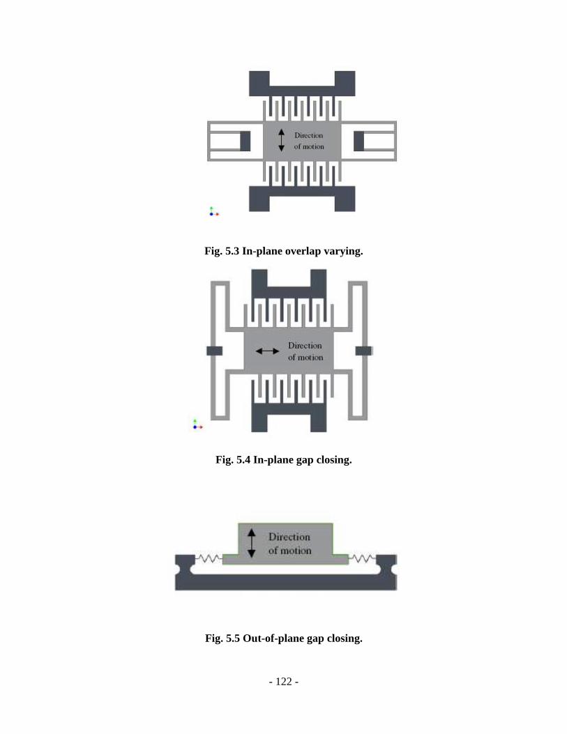
- 122 -
Fig. 5.3 In-plane overlap varying.
Fig. 5.4 In-plane gap closing.
Fig. 5.5 Out-of-plane gap closing.

- 123 -
Electromagnetic generators
The Faraday effects tells us that the electric current can be induced if the magnetic
flux is changing inside the conducting loop. In the real case, a conducting coil is usually
used, and the relative movement between the coil and the permanent magnet provides the
flux change. The open circuit voltage depends on the change rate of the flux and the
number of the loops in the coil. A micro-electromagnetic energy harvester was proved to
generate an output power of 400 µW, shown in Fig. 5.6[5.28]. Another electromagnetic
Fig. 5.6 Electromagnetic energy harvesting mechanism.
generator based on four moving magnets and a fixed coil demonstrated a peak output
power of 3.9 mW and an average power of 157 µW. [5.29] An electromagnetic micro-

- 124 -
cantilever device with a volume of 0.15cm3 was reported to generate a maximum power
46µW at 52Hz and an acceleration of 0.59m/s2.[5.10] A planar coil based structure was
investigated, with a polyimide film as the spring, a NdFeB magnet. The coil was made
from a 1.5 µm thick aluminum layer. [5.30]
5.1.3 Key Materials of Vibration Energy Harvesting Devices
Most of the vibration energy harvesters have applied smart materials, except for
those based on the relative movement between the magnets and the coil. Generally, smart
materials employed by vibration energy harvesters insist three types: piezoelectric,
magnetostrictive and high permeability material. The first two are traditional and widely
applied. They could not only work independently as the key material in the device, but
also combined to make a double layer or sandwich structure. The last was proved lately
to provide a high magnetic flux change rate with a fixed magnet pair, so as to generate
very high output power and provide very broad working bandwidth. Table 5.3 shows a
comparison between the energy harvesting behaviors of these materials.

- 125 -
Table 5.3 Comparison between different materials applied in vibration energy
harvesting system
Type Advantages Disadvantages
Piezoelectric
Direct conversion between
mechanical and electrical
energy, combine with
MEMS technology, small
size
Brittle, eddy current, suffer
from degraded polarization
after a certain time of
service, narrow bandwidth
Magnetostrictive Mechanically reliable
Bias magnetic field and coil
required, low efficient,
narrow bandwidth, narrow
bandwidth
Piezoelectric +
magnetostrictive
Able to harvest both
vibration and AC magnetic
energy, strong coupling,
high output
Two phases part from the
adhesive after a certain time
of deforming, large bias
magnetic field generally
required, narrow bandwidth
High Permeability Mechanically reliable,
broadband, very high output Magnets and coil required

- 126 -
Piezoelectric Material
Piezoelectric material has advantages like easy operation and direct conversion
between mechanical energy and electric energy. As a result it is the most widely used
material in the vibration energy harvesting application. And it is widely available in many
forms including single crystal (e. g. quarts), piezoceramic (e. g. lead zirconate titanate or
PZT), thin film (e. g. sputtered zinc oxide), screen printable thick-films based upon
piezoceramic powders and polymeric materials such as polyvinylidenefluoride (PVDF).
[5.18] The piezoelectric strain constant, d, is defined as =
m/V , or =
C/N . The piezoelectric effect has two working modes:
transverse mode d31 and longitudinal mode d33. A power density of 70 µW/cm3 has been
demonstrated with the PZT bimorph. [5.31]
Magnetostrictive Material
Magnetostriction is defined as the change of the physical dimension of a material in
response to the bias magnetic field or its magnetization change. The magnetostriction
coefficient λ is to describe this effect and it saturates with λs. Typical magnetostrictive
materials applied in vibration energy harvesting systems are Terfenol-D
(Tb0.3Dy0.7Fe1.9-2), crystalline alloy (ETREMA Products) and Metglas 2605
(Fe81B13.5Si3.5C2) metallic amorphous. Table 5.4 shows the magnetostriction constants
of different soft magnetic materials.

- 127 -
Table 5.4 The magnetostriction constants of different soft magnetic materials.
Conversely, inverse-magnetostriction also known as Villari Effect is defined as the
change in permeability subject to the mechanical stress on the material. This effect is
often applied in some vibration energy harvesters only with the existence of a bias DC
magnetic field to make sure the net magnetization in the material in one direction. The
Teffnol bar based harvester is able to generate an induced voltage of 150 V at 1 kHz, with
0.25 Ω resistances and a bias field of 200 Oe. [5.32] A cantilever of adhesive bonded six
layers of magnetostrictive Metglas 2605SC ribbon in a solenoid was claimed to generate
a maximum output power of 900µW at 1g. [5.15]
Composite of Piezoelectric and Magnetostrictive Material
The combination of piezoelectric and magnetostrictive material basically lay off the
picking coil for the magnetostrictive phase, since the mechanical deform transfers from

- 128 -
one phase to the other.[5.33] An electromagnetic micro-cantilever device with a volume of
0.15cm3 was reported to generate a maximum power 46µW at 52Hz and an acceleration
of 0.59m/s2. [5.12] A sandwich structure consisting of two piezoelectric layers and one
magnetostrictive layer, or name as magnetoelectric (ME) sensor structure, was able to the
maximum power 10.8mW at 60Hz and 0.1g acceleration with a total device volume
113cm3, due to the vibration induced magnetization change in the magnetostrictive layer.
[5.14] A magnetoelectric energy harvester with a beam consisting of both magnetostrictive
and piezoelectric phases was demonstrated to generate an output voltage of 4V under a
vibration acceleration of 0.05g at 20Hz and an AC magnetic field amplitude of 2Oe.[5.12]
High permeability material
High permeability material also known as soft magnetic material is easily magnetized
by a bias magnetic field. The magnetic flux density could be fairly high compared with
the other magnetic materials, when external magnetic field is applied. The
electromagnetic harvesting mechanism basically requires high flux change inside the
solenoid according to Faraday’s law, described as
! = "
= " ⋅ #
, (5.1)
where N is the number of coil turns, Φ is the magnetic flux of each turn, t is time, µ is the
effective permeability of the core. High permeability material applied as the core can
dramatically increase the induced voltage.
Some commercially available high permeability materials are Metglas 2605 S3A with
µr=35000 and saturation induction 1.41T, Metglas 2714A with µr=1,000,000 after

- 129 -
annealing and saturation induction 0.57T and MuShield with a maximum permeability of
300,000 and a saturation magnetization of 7500 Gauss.
5.2 Wideband Vibration Energy Harvester with High
Permeability Material
5.2.1 Introduction
The conventional vibration energy harvesters are designed as linear resonant
structures with narrow operating bandwidths, making them impractical when applied in a
real world environment which provides vibration sources with a wide frequency spectrum.
As a result, efforts have been made to explore non-linear mechanism that leads to wide
working bandwidth of vibration energy harvesters.
In this section, a schematic model of a novel wideband vibration energy harvester
would be discussed. The employing of the high permeability material generates a strong
magnetic coupling, leading to non-linear effect.

- 130 -
5.2.2 Basic Mechanism
Fig. 5.7 The section view of the schematic design of the vibration energy harvesting device.
Dimension of each part is: 4.4cm ×3.2cm×4cm for the solenoid, 1.25cm×2.2cm×1.5cm for
the magnet pair including the gap in between, 1.3cm×1.5cm×2.5cm for the mounting frame
on one side and 0.5cm×1.5cm×0.6cm on the other.
In this work, an alternative vibration energy harvesting model is set up and
experimentally verified, which is based on the strong magnetostatic coupling between the
cantilever beam and a bias magnet pair. The inhomogeneous bias magnetic field enables
the highly permeable beam to experience complete magnetic flux reversal twice in one
vibration period, which leads to maximized magnetic flux change rate in the solenoid. At
the same time, the magnetic potential energy makes the cantilever vibrate in a wider
potential well than in the simple harmonic case, which allows a wide working bandwidth
of the harvester. Schematic design of the vibration energy harvester is shown in Fig. 5.7.

- 131 -
The key component of this energy harvester is a high permeability (high-µ) single layer
beam, with one end fixed and the other end vibrating inside a solenoid. Two identical
rectangular hard magnets are placed in close proximity to the free end of the high-µ beam
Fig. 5.8 Magnet pair with antiparallel magnetic moment provides closed magnetic field lines,
making sure the maximum magnetic flux change, from Φ to –Φ during the vibration.
outside the solenoid to induce a non-homogeneous bias field which acts to induce
magnetization reversal. The bias magnets are aligned in parallel with each other, and
parallel to the beam. As shown in Fig. 5.8, magnets form a closed flux with the
magnetizations antiparallel to each other. When the free end of the cantilever passes
through the spatially inhomogeneous fringing magnetic field generated by the bias
magnet pair, the magnetization of the magnetic cantilever would be reversed by the

- 132 -
antiparallel bias magnetic field by 180°. The magnetization reversal in the magnetic
Fig. 5.9 Magnet pair with parallel magnetic moment provides repelling magnetic field lines,
in which case the magnetic flux changes from Φ to 0 and back to Φ during the vibration.
cantilever leads to maximized flux change in the solenoid, resulting in an induced voltage
which varies at the same frequency of the mechanical vibrating source. However, when
the magnetization of the two bias magnets in parallel, as shown in Fig. 5.9, the repulsing
magnetic field would keep the beam magnetized towards the same direction all the time.
As a result, the magnetic flux change will be smaller in this case compared to that in the
antiparallel case in Fig. 5.8, leading to a lower output voltage and an induced AC voltage
with a frequency that is double of that of the mechanical vibration frequency.

- 133 -
5.2.3 Prototype and Testing System
The harvester, including the MµShield® cantilever, the solenoid and a SmCo
magnet pair, is seated on a vibrating stage, as shown in Fig. 5.10. The stage is driven by
an audio power amplifier connecting to a lock-in amplifier. The mechanical movement of
Fig. 5.10. Prototype of the wideband high permeability vibration energy harvester.
the stage is monitored by an accelerometer. Voltage output of the harvester in time
domain is monitored by a digital oscilloscope. Total volume of the energy harvester is
68.96cm3, including the solenoid with the beam inside, the magnet pair with the gap in
between and the mounting structure. The coil resistance of the solenoid is 1 Ohm, the

- 134 -
inductive impedance is 2.86 Ohm at 54 Hz, which is obtained by measurement. A lead tip
mass is attached on the free end to adjust the vibration amplitude and the intrinsic
frequency, which weighs 0.5 g.
5.2.4 Theoretical Model
The total induced voltage across the coil could be predicted by doing integral
along the solenoid, shown in 5.11, because the magnetic field magnitude varies along the
Fig. 5.11. The Schematic of the calculation of induced voltage across the solenoid.
beam. According to Faraday’s law the open circuit voltage can be expressed by:
0 0[ , ( )] [ , ( , )] [ , ( , )]( )open
d H x y x M x y x t A dN d M x y x t A dNd tV
dt dt dt
µ µφ + ⋅ ⋅ ⋅ ⋅= = =∫ ∫ ,
(5.2)

- 135 -
where M is the magnetization in the beam , A is the cross section area of the beam and
dN the number of loops in the infinitesimal length unit of the solenoid dx, shown in Fig.
5.11, and
L
w
NdN dx
d= . (5.3)
NL is the number of coil loop layers in the solenoid and dw is the copper wire diameter of
Fig. 5.12 Hysteresis loop of the MuShield beam with the dimension of 4.6cm × 0.8cm × 0.0254cm.
the coil. The dimension of the beam is 4.6cm × 0.8cm × 0.0254cm, with a length: width:
thickness ratio 181:31.5:1, which makes sure that the length direction is the magnetic
easy axis. It has a maximum permeability of 300,000 and a saturation magnetization of
7500 Gauss. The magnetic hysteresis loop M(H) along the length direction of the beam

- 136 -
was measured, shown in Fig. 5.12, in order to calculate the magnetization M[x,y] at an
arbitrary point on the beam in the non-uniform magnetic field. Vibration amplitude of an
arbitrary point on the beam y(x,t) is got by combining solutions of Euler–Bernoulli beam
equation y(x) and the equation of motion for the cantilever y(t). According to the Euler-
Bernoulli equation and boundary conditions, the maximum deflection of the cantilever is
$%& = !" "
! [5.34], as shown in Fig. 5.13. By combing the time dependent term a(t),
Fig. 5.13. Beam shape at its maximum deflection.
the beam shape function at time t is
2 3
3
3( , ) ( )( )
2
Lx xy x t a t
L
−= , (5.4)

- 137 -
where L is the length of the beam and a(t) is the amplitude at free end, which is
determined by the following equation of motion,
'
= −
#
− () $&+ *$% , (5.5)
meff is the effective mass of the beam plus tip mass at the free end, which is 0.74g. The
first term on the right hand side dU
da− is the total force due to the total potential energy,
( )magnetic elasticd U UdU
da da
+= , (5.6)
where the elastic potential energy 2
2elastic
kU a= , with k the elasticity coefficient which is
experimentally determined to be 77N/m, and magneticU the magnetic potential due to the
bias magnet pair
+&'( , −-./0%,$&1 ∙ 2'../,!
(5.7)
in which is the magnetic moment in the beam. Size of the identical SmCo hard magnet
is 2.2cm × 1.3cm × 0.2cm, providing a fringing magnetic field ~500Oe at the free end of
cantilever and ~10Oe in the middle of the solenoid. The distribution of magnetic field is
obtained with discrete spatial magnetic field measurements and fitted with simulation.
The second term − in equation (5.5) is the mechanical damping term, with b the
damping constant which is experimentally determined to be 0.0024Ns/m. The third term
Fdrive stands for the vibration driving force applied on the fixed end, which is a sine wave
input.
When a load resistance is connected across the coil, the vector voltage across
each element has the relationship = + + . The solenoid is

- 138 -
equivalent to a resistance in series with an inductance. The output power is optimized
when the impedance is matched, 1
22L CX fL X
fCπ
π= = = and load coilR R= , which
could be done by inserting a capacitance and adjusting the load resistance. In this way,
the maximum output power is
[ ]2
22
max 0
0
2 , ( , )1
4
openL
L
load load w
VdM x y x tN
P A dxR R d dt
µ
= =
∫ . (5.8)
Equation (5.8) indicates that at a particular frequency, the output power depends
on the change rate of magnetization in the beam.
5.2.5 Results and Discussion
Figure 5.14 shows calculated and measured results of the open circuit voltage in
two cases. When the magnet pair is set to have antiparallel magnetization, the energy
harvester shows a high open circuit voltage with a peak value 544mV at a vibration
frequency of 54Hz and acceleration of 0.57g. As expected, the output voltage with a
doubled frequency 108Hz with a significantly lowered peak value of 8mV was observed
for the case when the two bias magnets are arranged with parallel magnetization. It is
interesting to note that the mechanical vibration source is a sine wave signal, while the
output voltage is not, but with narrow peaks with a full width at half maximum of 1ms.
This is related to the nonuniform magnetic field spatial distribution, leading to the
approximate square wave time varying magnetic flux, shown in Fig. 5.15. The free end
amplitude dependent flux is also plotted. It is clear that the flux in the beam is reversed
immediately while passing the nonstable equilibrium position in the middle. The sharp

- 139 -
Fig. 5.14 Measured and calculated results of the open circuit voltage for the energy
harvesting device at the mechanical vibration frequency 54 Hz, acceleration 0.57 g (g=9.8
m/s2).
drop and rise in flux is the reason for large induced voltage.
Figure 5.16 shows the frequency response of the harvester. The maximum
measured output power is 74mW on a 1Ω load and with a time average value 5mW at an
acceleration 0.57g corresponding to a maximum power density of 1.07 mW/cm3 or 1.88
mW/g cm3.

- 140 -
Fig. 5.15 Normalized magnetic flux as a function of time and free end amplitude, at
vibration frequency of 54 Hz, acceleration 0.57 g.
Fig. 5.16 Measured and calculated frequency response of the energy harvester.

- 141 -
5.2.6 Nonlinear Effect
From Fig. 5.16, we can see that the working bandwidth is about 10Hz, 18.5% of
the central frequency, compared with 2.1Hz [5.14] or 3.5% of the central frequency, for a
typical linear oscillator harvester. The major reason for the large bandwidth is that the
magnetic coupling is not linear to the displacement of the oscillator, so that the nonlinear
effect provides the system a wider working bandwidth. [5.35] As shown in Fig. 5.17,
Fig. 5.17 Elastic potential energy, magnetic potential energy and total potential energy of
the oscillation system as functions of free end displacement of the beam.
compared with the elastic potential energy, the magnetic potential energy curve has
double potential wells closely connected, resulting in a wider well. As long as the

- 142 -
acceleration is larger than its threshold value, or when the cantilever is supplied with
enough energy to get over the barrier in the middle, it can vibrate between two shallow
potential wells, realizing a relatively wide oscillation region at a particular driving
frequency. However, if the oscillator is not supplied with enough energy or the damping
is so strong that it is not able to get over the potential barrier, the oscillation is limited in
one well, instead of two. In this case, the behavior of the oscillator is more like that of a
linear one, with narrow working bandwidth.
Both the calculated and measured curves in Fig. 5.16 exhibit unsymmetrical peaks
about the central frequency. This is because the performance of the oscillator at lower
band differs from that at higher band. At lower band, the oscillation behavior is
dominated by nonlinear effect. The output power decreases slowly as the frequency
reduced, simply due to the mismatch between the intrinsic and driving source frequency.
Even if at a frequency as low as 30 Hz, oscillation between two potential wells was still
observed. However, in higher frequency range than 54 Hz, the performance is dominated
by linear effect and oscillator was observed trapped in one well, leading to one sided
narrow peaks in the voltage signal. This is because in higher frequency range, larger
dynamic speed results in larger damping force, so that the cantilever does not have
enough energy to climb over the potential barrier in the middle. This single well
oscillation dramatically decreases the harvesting efficiency because the cantilever beam
can hardly reach flux reversal.

- 143 -
5.2.7 Advantage of High Permeability Vibration Energy
Harvesting
Table 5.2 shows the figures of merit for vibrating energy harvesters with different
types of working mechanisms and materials, including magnetoelectric, electrostatic,
piezoelectric, magnetoelectric sensor based, magnetostrictive and high permeability
material based devices. Among all these different mechanisms and products, this high-µ
energy harvester, which is based on the magnetic interaction between the vibrating high-
µ beam and the bias hard magnets, generates relatively high power density and wide
working bandwidth. Besides, the single layer metallic high-µ beam does have advantages
from the material point of view. First of all, it is mechanically more robust compared
with most of the piezoelectric materials or glue bonded multilayer materials. Secondly,
the single layer metallic high-µ beam does not have problems of degraded performance
after a certain working time.
5.2.8 Summary
In summary, an energy harvesting platform was theoretically studied and tested,
which incorporated a vibrating high permeability cantilever, a solenoid and a bias magnet
pair. Interaction between the high permeability magnetic beam and the bias magnets
leads to complete flux reversal of the high permeability beam, which generates a
maximum power of 74 mW and a high power density of 1.07 mW/cm3at 54 Hz at an
acceleration of 0.57g. The inhomogeneous magnetic field leads to a non-linear magnetic
force on the high permeability beam, resulting in a nonlinear oscillator with a wide
working bandwidth of 10 Hz or 18.5% of the operating frequency. This alternative

- 144 -
energy harvesting platform using high permeability magnetic materials provides great
opportunities for energy harvesters that have high power output and wide working
bandwidth.
5.3 High Output Vibration Energy Harvester with High
Permeability Material
5.3.1 Introduction
Vibration energy harvesting technologies have been developing rapidly, and have
shown great potential in many different applications. However, these applications have
been severely limited by the amount of energy that can be harvested. Achieving high
power and high power density vibration energy harvesters, which has attracted a lot of
recent interests, will enable a much wider range of applications for vibration energy
harvesters [5.36, 5.37]. So far, piezoelectrics based vibration energy harvesters which have
received the most amount attention, have demonstrated much higher power density than
their magnetic based counterparts, even though most piezoelectric based energy
harvesters show a narrow bandwidth or a limited operating frequency range of 2~5% of
the center operating frequency. For example, a piezoelectric bare beam based vibration
energy harvester can generate a power of 6.63 mW/cm3 [5.13]. Nevertheless, theoretically,
the magnetostatic energy density 1/2µH2 in high permeability magnetic materials is
105~106 times that of the electrostatic energy density 1/2εE2 in piezoelectrics [5.38].
Vibration energy harvesters with hard or soft magnetic materials have been studied and
tested [5.39, 5.40, 5.41]. However, the full potential of achieving high power density in

- 145 -
vibration energy harvesters with high permeability magnetic materials has not yet been
realized.
This section discusses about an alternative design of a vibration energy harvester,
which was demonstrated to significantly increase the output power density, by utilizing
the strong magnetostatic interaction between solenoids with high permeability magnetic
materials and vibrating hard magnet pair. There are two main reasons for improved
output power density. First, more layers of high permeability materials served as the
induction core than the first generation design, discussed in section 5.2. Besides, the
magnetostatic energy on both sides of the magnets was utilized by placing one solenoid
on each side.
5.3.2 Basic Mechanism
The schematic design of the energy harvester is shown in Fig. 5.18. Two identical
solenoids with high permeability/insulator multilayer cores were placed at two sides of a
vibrating hard magnet pair with anti-parallel magnetization. The key components of this
energy harvester are the two identical solenoids with a high permeability (high-µ)
MuShield® core inside which are placed at two sides of the magnet pair and fixed on a
vibrating stage. The magnet pair is placed with the two magnets having anti-parallel
magnetization and supported by a regular circular cross-section spring with its bottom
fixed on the surface. When the magnet pair moves up and down with respect to the
vibrating stage, the magnetic field inside each solenoid changes the direction periodically.
The magnetostatic coupling between the solenoids and the time varying inhomogeneous
bias magnetic field results in a non-linear oscillation and a complete magnetic flux

- 146 -
Fig. 5.18 The schematic design and working mechanism of the high power vibration energy
harvester. (a) The magnet pair moves to the top. (b) The magnet pair moves to the bottom.
reversal in the solenoids. The presence of highly permeable cores dramatically increases
the magnitude of magnetic flux inside the coils. Thus, a large induced voltage is
generated on both sides of the solenoid, and the output voltage can be doubled with serial
connection of the two solenoids.
5.3.3 Theoretical Analysis
The mass of the hard magnet pair, the stiffness of the supporting spring and the
magnetostatic coupling between the solenoids and hard magnet pair together determine
- 147 -
the resonance vibration frequency and the output voltage of the energy harvester. The
equivalent spring-mass system becomes a non-linear oscillation system due to the
magnetostatic coupling between the solenoids and the hard magnet pair. This non-linear
effect can be explained from the potential energy point of view, as explained in section
5.2. The elastic potential energy of a spring-mass system is a well-know linear one, with
only one minimum value, which happens when the mass passes the equilibrium position
in the middle. In contrast, the magnetostatic potential energy has two identical minimum
values due to the coupling between the magnets and solenoids, which appear when the
magnets move a short distance up or down from the equilibrium position in the middle.
As a result, the superposition of two different types of potential energy make a non-linear
one, leading to a wider oscillation frequency range, as has been shown in Fig. 5.17.
The total induced voltage equals the integral over the whole solenoid, because the
magnetic field varies along the axis. The open circuit voltage can be expressed by:
dt
dNAtxyxMtyxHd
dt
tdV ∫ ⋅⋅+== )],(,[4)](,[
2)(
2πφ
dt
dNAtxyxMd∫ ⋅⋅=
)],(,[42
π, (5.9)
where A is the total cross section area of the multilayer cores, dN is the number of loops
in the infinitesimal length unit of the solenoid, and
wddx
LNdN ⋅= . (5.10)

- 148 -
NL is the number of loop layers and dw is the copper wire diameter. Hence, the maximum
output power, which happens when the load impedance equals the conjugate of the output
impedance of the solenoid coil, is
( ) 2
0
22
max )],(,['162
== ∫
L
w
L
coilcoil
dxdttxyxdM
d
NA
R
S
R
VP π , (5.11)
where S is the number of layers in each core and A' is the cross section area of one layer.
Equation (5.11) indicates that the output power increases as the resonance frequency
increases, if all other parameters are kept constant. Certainly, for the same source power,
amplitude would be reduced if the frequency gets higher. Moreover, at a particular
frequency, the output power depends on the total magnetic flux change in the solenoid in
one oscillation period, which is directly related to the permeability of the magnetic cores.
The solenoid with soft magnetic MuShield® core, which has a high permeability, has a
great potential for generating a high voltage output. Meanwhile, the multilayer structure
of MuShield® material is expected to generate a much larger flux change than a single
layer. The application of a single layer was discussed in the earlier section.
5.3.4 Prototype and Testing System
The entire device is powered by a vibrating stage, which is driven by an audio
power amplifier. Voltage output of the harvester in time domain is monitored by a digital
oscilloscope. The device picture is shown in Fig. 5.19. The SmCo hard magnet has a
dimension of 2.2cm × 1.3cm × 0.2cm. Each solenoid core is a 28-layer high permeability
MuShield material, with a dimension of 2cm × 2cm × .002 inches. Total volume of the
energy harvester is 6.44cm × 3.25cm ×1.4cm = 29.3 cm3, including the solenoids, the

- 149 -
magnet pair and the gap in between. The coil resistance of each solenoid is 1.3 Ohm.
Fig. 5.19 Structure of the vibration energy harvester. Dimension of each component is: 2 ×
2.5 × 1 cm3 for the solenoids, 1.25 × 2.2 × 1.5 cm3 for the magnetic pair, including the gap in
between.
5.3.5 Results and Discussion
Figure 5.20 indicates the measured open circuit voltage of the energy harvester
with different springs at resonance frequencies of each. For spring #1, with resonance
frequency 27 Hz, the peak voltage is 1.18 V for acceleration of 2g (g=9.8 m/s2); spring
#2, with resonance frequency 33 Hz generated maximum voltage of 1.64 V for
acceleration of 3g; spring #3, brought up peak voltage 2.52 V, with intrinsic frequency
42 Hz and acceleration of 5 g. Increasing acceleration values were applied to maintain
the same source vibration amplitude. The maximum output power on a 2.6 Ohm load is
133.88 mW, 258.62 mW and 610.62 mW, respectively, as shown in Fig. 5.21.

- 150 -
Considering the total practical volume of the device 29.3 cm3, this device has good
performance with the maximum power density, 20.84mW/ cm3 at 42 Hz with spring #3.
Q factor of the harvester at 42 Hz was 16, which was obtained from the decay curve of
output voltage when turning off the source [5.10]. Almost the entire device damping is
generated from the mechanical collision between the spring supported magnets and the
solenoid holder. That means a much lower input force or acceleration is needed and
Fig. 5.20 Measured results of the open circuit voltage for the energy harvesting device with
three different springs at respective resonance frequencies: spring #1 at 27 Hz; spring #2 at
33 Hz and spring #3 at 42 Hz.
much higher Q factor could be reached by using better crafting technique. A simple
relation between frequency and power can be derived from Eq. (5.11), Pmax ~ 2
∆∆
T
M ~

- 151 -
f 2, if all other parameters kept constant, where ∆M is the flux change per period and ∆T
Fig. 5.21 Measured maximum output power of the harvester with three different springs, at
resonance frequency of each.
the period. In fact, the measured results agree with the parabolic curve fitting, as shown
in Fig. 5.21. Clearly this vibration energy harvester design can accommodate different
vibrating frequencies of the environment by changing the spring that is connected to the
hard magnet pair. If the vibration amplitude of the testing stage kept the same, the output
power and power density are proportional to the second power of the vibration frequency.
Hence, if this Pmax~f2 can be extrapolated to higher frequencies, much higher output
power density can be achieved on condition of constant amplitude. It is noticeable that
large working bandwidth could still be obtained at high frequency due to the non-linear
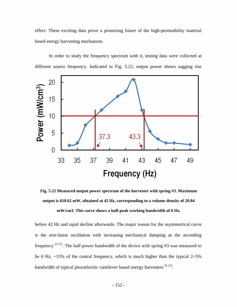
- 152 -
effect. These exciting data prove a promising future of the high-permeability material
based energy harvesting mechanism.
In order to study the frequency spectrum with it, testing data were collected at
different source frequency. Indicated in Fig. 5.22, output power shows sagging rise
Fig. 5.22 Measured output power spectrum of the harvester with spring #3. Maximum
output is 610.62 mW, obtained at 42 Hz, corresponding to a volume density of 20.84
mW/cm3. This curve shows a half-peak working bandwidth of 6 Hz.
before 42 Hz and rapid decline afterwards. The major reason for the asymmetrical curve
is the non-linear oscillation with increasing mechanical damping as the ascending
frequency [5.37]. The half-power bandwidth of the device with spring #3 was measured to
be 6 Hz, ~15% of the central frequency, which is much higher than the typical 2~5%
bandwidth of typical piezoelectric cantilever based energy harvesters [5.13].

- 153 -
5.3.6 Advantages of the 2nd Generation High Permeability Vibration
Energy Harvester and Summary
Compared to the previous vibration energy harvester design based on a vibrating
high-µ beam and a stationary bias hard magnet pair, this new generation device has a new
structure that utilizes a vibrating hard magnet pair and a stationary solenoid pair with
thick multilayer high-µ core materials. The multilayer high permeability solenoids core
leads to significantly increased flux change in the solenoid within one period without
increasing the total volume of the device. In addition, the two solenoids at both sides of
the vibrating magnets make full use of the spatially inhomogeneous bias magnetic fields
at both sides of the magnets, leading to doubled power output, and a dramatically
enhanced power density by ~ 20X over the previous energy harvester design with high-µ
materials.
In summary, we investigated a 2nd generation of magnetic based vibration energy
harvesters, achieving a high power density larger than 20mW/cm3 with acceleration of 5
g, which is over 3 times of the best power density data reported for vibration energy
harvesters [5.13]. Unlike the piezoelectric cantilever based vibration energy harvesters that
suffer from narrow bandwidth and brittle cantilever and degraded polarization after a
certain time of service, the new generation vibration energy harvester design based on
multilayer high permeability magnetic material exhibits giant power density, high output
power and large bandwidth, which provides great opportunities for practical compact
energy harvesters.

- 154 -
REFERENCES
5.1 V. Raghunathan, C. Schurgers, S. Park and M. B. Skrivastava, Energy-Aware Wireless
Microsensor Networks IEEE Signal Process. Mag. 19 40-50, (2002).
5.2 G. Park, T. Rosing, M. Todd, C. Farrar and W. Hodgkiss, “Energy Harvesting for
Structural Health Monitoring Sensor Networks”, Journal of Infrastructure Systems,
March, (2008).
5.3 S. J. Roundy, “Energy Scavenging for Wireless Sensor Nodes with a Focus on
Vibration to Electricity Conversion”, Ph.D. Dissertation, University of California,
Berkeley, (2003).
5.4 H. J. Goldsmid, “Thermoelectric Refrigeration”, New York, Plenum Press, (1964).
5.5 T. M. Tritt and M. A. Subramanian, “Thermoelectric Materials, Phenomena, and
Application: a Bird’s Eye View”, MRS Bulletin VOL. 31, Mar (2006).
5.6 K. Zorbas, E. Hand, K. M. Paraskevopoulos, “Power and Efficiency Calculation and
Evaluation of Material Properties in Thermoelectric Power Generators”, Mater. Res. Soc.
Symp. Proc. VOL. 1044, MRS, 1044-U09-15 (2008).
5.7 G. Chen, M. S. Dresselhaus, G. Dresselhaus, J. P. Fleurial and T. Caillat, “Recent
developments in thermoelectric materials, International Materials Reviews”, VOL. 48,
NO. 1, 45 (2003).
5.8 L. Mateu and F. Moll, “Review of Energy Harvesting Techniques and Applications for
Microelectronics”, Proceedings of the SPIE Microtechnologies for the New Millenium,
(2005).

- 155 -
5.9 D. Mascarenas, “Development of an Impedance Method Based Wireless Sensor Node
for Monitoring of Bolted Joint Preload”, (2006)
5.10 S. P. Beeby, R. N. Torah, M. J. Tudor, P. Glynne-Jones, T. O’Donnell, C. R. Saha and
S. Roy, J. Micromech. Microeng. 17, 1257 (2007).
5.11 G. Despesse, T. Jager, J. Chaillout, J. Leger, and S. Basrour, Ph.D. Research in
Microelectronics and Electronics, 1, 225 (2005).
5.12 S. X. Dong, J. Zhai, J. F. Li, D. Viehland, and S. Priya, Appl. Phys. Lett. 93, 103511
(2008).
5.13 http://www.mide.com/products/volture/v25w/v25w.php
5.14 http://www.ferrosi.com/files/VEH360_datasheet.pdf
5.15 L. Wang, F. G. Yuan, Smart Material and Structures 17, 045009 (2008).
5.16 http://www.perpetuum.co.uk/resource/PMG37%20-%20Technical%20Flyer%20Iss%
20C.pdf
5.17 http://www.kcftech.com/products/documents/WSKdatasheet.pdf
5.18 S. P. Beeby, M. J. Tudor and N. M. White, “Energy Harvesting Vibration Sources for
Microsystems Applications”, Meas. Sci. Technol. 17, R175-R195 (2006).
5.19 M. Kimura, “Piezo-Electricity Generation Device”, US Patent (1998).
5.20 T. Starner, “Human-Powered Wearable Computing”, IBM syst. J. 35 618-29, 1996.
5.21 N. S. Shenck and J. Paradiso, “Energy Scavenging with Shoe-Mounted
Piezoelectrics”, IEEE Micro, may-June, P. 30, 2001.
5.22 S. P. Beeby, R. N. Torah, M. J. Tudor, T. O’Donnell, C. R. Saha, S. Roy, Power
MEMS, Nov. 29th – Dec. 1st (2006).

- 156 -
5.23 Y. B. Jeon, R. Sood, J. Jeong and S. G. Kim, “MEMS Power Generator with
Transverse Mode Thin Film PZT”, Sensors Actuators A 122 16-22 (2005).
5.24 K. Dogheche, B. Cavallier, P. Delobelle, L. Hirsinger, E. Cattan, D. Remiens, M.
Marzencki, B. Charlot, S. Basrour and S. Ballandras, “A Bi-Stable Micro-Machined
Piezoelectric Transducer for Mechanical to Electrical Energy Transformation”, Integrated
Ferroelectrics, VOL. 80, NO. 1, pp. 305-315(11) (2006).
5.25 R. X. Gao and Y. Cui, Proc. SPIE 5765, 794 (2005).
5.26 S. Roundy, P. Wright and K. Pister, “Micro-Electrostatic Vibration-to-Electricity
Converters”, Proc. IMECE, pp 1-10 (2002).
5.27 S. Roundy, “Energy Scavenging for Wireless Sensor Nodes with a Focus on
Vibration to Electricity Conversion”, PhD Thesis University of California, Berkeley,
(2003).
5.28 R. Amirtharajah and A. Chandrakasan, “Self-Powered Signal Processing Using
Vibration-Based Power Generation”, IEEE Journal of Solid-State Circuits, VOL. 33, NO.
5, May (1998).
5.29 P. Glynne-Jones, M. J. Tudor, S. P. Beeby and N. M. White, “An Electromagnetic,
Vibration-Powered Generator for Intelligent Sensor Systems”, Sensors Actuators A, VOL.
110, pp. 344-349 (2004).
5.30 A. Perez-Rodriguez, C. Serre, N. Fondevilla, C. Cereceda, R. Morante, J. Esteve and J.
Montserrat, “Design of Electromagnetic Inertial Generators for Energy Scavenging
Applications”, Proceedings of Eurosensors XIX, Barcelona, Spain, paper MC5, (2005).
5.31 S. Roundy, P. K. Wright, and J. Rabaey, “A Study of Low Level Vibrations as a
Power Source for Wireless Sensor Nodes”, Computer Communications, 26, 1131 (2003).

- 157 -
5.32 X. Zhao and D. G. Lord, “Application of the Villari Effect to Electric Power
Harvesting”, J. Appl. Phys. 99, 08M703 (2006).
5.33 J. Huang, R. C. O’Handley and D. Bono, Proc SPIE 5050, 229 (2003).
5.34 F. P. Beer, E. R. Johnston and J. T. DeWolf, Mechanics of Materials, 3rd Edition,
McGraw-Hill Book Company, Inc., New York, (2002).
5.35 F. Cottone, H. Vocca, and L. Gammaitoni, Phys. Rev. Lett. 102, 080601 (2009).
5.36 S. Roundy, P. K. Wright, and K. Pister, Proceedings of 2002-34309, New Orleans,
LA, 17-22 (2002).
5.37 X. Xing, J. Lou, G. M. Yang, O. Obi, C. Driscoll and N. X. Sun, Appl. Phys. Lett. 95
(13) (2009).
5.38 J. W. Judy, Smart Mater Struct 10 (6), 1115-1134 (2001).
5.39 S. Kulkarni, S. Roy and T. O’Donnell, J. Appl. Phys. 99, 08P511 (2006).
5.40 S. Kulkarni, E. Koukharenko, R. Torah, J. Tudor, S. Beeby, T. O’Donnell and S. Roy,
Sensors and Actuators A, 145-146, 336-342 (2008).
5.41 S. Kulkarni, S. Roy, T. O’Donnell, S. Beeby and J. Tudor, INTERMAG 2006, 317-
317 (2006).

- 158 -
6 Conclusion and Future Work
The basic magnetic properties of soft magnetic materials were discussed in this
work, including the low coercive field and high magnetization. The widely used
experimental methods of magnetic films were introduced. All the FeCoB films related to
this work were deposited with the physical vapor deposition system. Some typical
magnetic material characterization methods were explained. The vibrating sample
magnetometer (VSM) is used to detect and plot the quasi-static magnetic field response
of the magnetic material. The ferromagnetic resonance curve shows the high frequency
magnetic loss.
A series of sandwich structure of FeCoB(100nm)/Al2O3/FeCoB(100nm) was
made with the PVD system and studied, in order to find the optimized thickness of the
Al 2O3 insulating layer. It was found that the anti-ferromagnetic coupling exists when the
Al 2O3 thickness is lower than 6 nm, resulting a higher coercive field and FMR linewidth.
As a result, a minimum thickness of 6 nm of Al2O3 should be achieved when applying the
FeCoB multilayer structure for high frequency energy applications.
The magnetron sputter deposition technology is compatible with the on-chip
micro-fabrication method. On Si chip integrated inductors applying the FeCoB/Al2O3
multilayer core structure were designed, fabricated and tested. Three different types of
solenoid inductors were designed, with the same area but different shape of cores. The
theoretical model was discussed in order to analyze the inductance, resistance and quality
factor. The on-chip micro-fabrication process was designed as discussed. The testing

- 159 -
technique which requires a vector network analyzer and a probe station was introduced,
as well as the de-embedding and parameter extracting method. After the measurement,
the inductance and quality factor curves were plotted. A maximum inductance of 60 nH
was obtained at low frequency. It was found that the inductance increases with the
number of turns when keeping the other variables unchanged. The magnetic loss gets
lower when the core was divided into two separate parts. However, the electrical loss
increases because the total number of turns doubles for the two-sided design. A
comparison between the inductors with and without the magnetic cores was done by
plotting their inductance or quality factor curves together. The inductance was increased
by a factor of 3.6 ~ 6.7 with the magnetic cores. The magnetic loss due to the core is very
high, so the magnetic annealing process is very necessary to improve the magnetic core,
which will be done in the future. Also, the on chip integrated transformer could be
studied, which shares the same fabrication process.
The soft magnetic materials also play an important role in serving some other
energy related applications, such as the vibration energy harvesting system. Two
generations of high permeability material applied vibration energy harvesting devices
were designed, made and tested. The strong magnetic coupling between the magnets and
the high permeability material is able to generate a large induced voltage across the
solenoid, when they have relative vibration. This coupling also generates the magnetic
potential energy of the oscillation system, which enables the so called non-linear effect,
leading to a wide working bandwidth of the devices. The 1st generation of vibration
energy harvester was able to generate 74mW on a 1Ω load and with a time average value
5mW at an acceleration 0.57g corresponding to a maximum power density of 1.07
- 160 -
mW/cm3 or 1.88 mW/g cm3. Meanwhile, the device had a working bandwidth as wide as
10 Hz/ 54 Hz. The design of the 2nd generation was improved, so that the magnetic
energy on both sides of the magnets could be utilized. This device was proved to be able
to generate 610.62 mW at 42 Hz, corresponding to a volume density of 20.84 mW/cm3
with a half-peak working bandwidth of 6 Hz. The energy loss in this design mainly came
from the mechanical dissipation between the parts of the device. The efficiency could be
significantly improved in the future if the joint parts are re-designed and made with more
professional machines.
In summary, the application of soft magnetic materials with high permeability
was done on two different energy related topics: on chip integrated inductors and
vibration energy harvesting. The decent testing results of all devices proved the
feasibility and potential.