Embed Size (px)
Citation preview
LMK01801
www.ti.com SNAS573A –JANUARY 2012–REVISED APRIL 2013
LMK01801 Dual Clock Divider BufferCheck for Samples: LMK01801
1 Device Summary
1.1 Features12
• 6 Differential Outputs (or up to 12 as• Pin Control Mode or MICROWIRE (SPI)LVCMOS)• Input and Output Frequency Range 1 kHz to 3.1
• Divides Values of 1 to 1045 or 1 to 8,GHzEven and Odd• Separate Input for Clock Output Banks A & B.
• Analog and Digital Delays• 14 Differential Clock Outputs in Two Banks (A• 50% Duty Cycle on All Outputs for All Divides& B)• Separate Synchronization of Bank A and B.– Output Bank A• RMS Additive Jitter 50 fs at 800 MHz• 8 Differential, Programmable Outputs (Up
to 8 as LVCMOS) – 50 fs RMS Additive Jitter (12 kHz to 20 MHz)• Divider Values of 1 to 8, Even and Odd. • Industrial Temperature Range: -40 to 85 °C
– Output Bank B • 3.15 V to 3.45 V Operation
1.2 Target Applications• High Performance Clock Distribution and Division• Wireless Infrastructure• Datacom and Telecom Clock Distribution• Medical Imaging• Test and Measurement• Military / Aerospace
1.3 Description
The LMK01801 is a very low noise solution for clocking systems that require distribution and frequencydivision of precision clocks.
The LMK01801 features extremely low residual noise, frequency division, digital and analog delayadjustments, and fourteen (14) programmable differential outputs: LVPECL, LVDS and LVCMOS (2outputs per differential output).
The LMK01801 features two independent inputs that can be driven differentially (LVDS, LVPECL) or insingle-ended mode (LVCMOS, RF Sinewave). The first input drives output Bank A consisting of eight (8)outputs. The second input drives output Bank B consisting of six (6) outputs.
1
Please be aware that an important notice concerning availability, standard warranty, and use in critical applications ofTexas Instruments semiconductor products and disclaimers thereto appears at the end of this data sheet.
2All trademarks are the property of their respective owners.
PRODUCTION DATA information is current as of publication date. Products conform to Copyright © 2012–2013, Texas Instruments Incorporatedspecifications per the terms of the Texas Instruments standard warranty. Productionprocessing does not necessarily include testing of all parameters.

Test/CLKoutTYPE_0
EN_PIN_CTRL
SYNC1/CLKoutTYPE_2
SYNC0/ CLKoutTYPE_1
CLK
in0C
LKin0*
CLKout0
CLKout1CLKout1*
CLKout13
CLKout13*
CLKout12CLKout12*
Mux
Mux
CLK
in1C
LKin1*
CLKuWire/CLKoutDIV_1
DATAuWire/CLKoutDIV_0
LEuWire/CLKoutDIV_2
ControlRegisters
PWirePort
AnalogDelay
Divider(1-1045)
Digital Delay
CLKout2
CLKout2*
CLKout3CLKout3*
CLKout4
CLKout4*CLKout5
CLKout5*
CLKout6
CLKout6*CLKout7
CLKout7*
Divider(1-8)
Divider(1-8)
Bank A Bank B
Device Control
CLKout0*LVDS/LVPECL
LVDS/LVPECL/LVCMOS
LVDS/LVPECL/LVCMOS
LVDS/LVPECL/LVCMOS
LVDS/LVPECL/LVCMOS
LVDS/LVPECL/LVCMOS
LVDS/LVPECL/LVCMOS
LVDS/LVPECL
Divider(1-8)
CLKout11
CLKout11*CLKout10CLKout10*
CLKout9
CLKout9*CLKout8CLKout8*
Divider(2-8)
Mux
Divider(2-8)
Mux
CG1 Divider
CG2 Divider
CG4 Divider
CG3 Divider
CLK
in0 Divider
CLK
in1 Divider
Clock D
istribution Path A
Clock D
istribution Path B
LMK01801
SNAS573A –JANUARY 2012–REVISED APRIL 2013 www.ti.com
1.4 Functional Block Diagram
2 Device Summary Copyright © 2012–2013, Texas Instruments Incorporated
Submit Documentation FeedbackProduct Folder Links: LMK01801
LMK01801
www.ti.com SNAS573A –JANUARY 2012–REVISED APRIL 2013
1 Device Summary ........................................ 1 6.9 CLOCK OUTPUT SYNCHRONIZATION ........... 15
1.1 Features ............................................. 1 6.10 DEFAULT CLOCK OUTPUTS ..................... 15
1.2 Target Applications .................................. 1 7 Functional Description ............................... 161.3 Description ........................................... 1 7.1 PROGRAMMABLE MODE ......................... 16
1.4 Functional Block Diagram ........................... 2 7.2 PIN CONTROL MODE ............................. 16
2 Device Information ...................................... 4 7.3 INPUTS / OUTPUTS ............................... 16
2.1 Functional Configurations ............................ 4 7.4 INPUT AND OUTPUT DIVIDERS .................. 16
2.2 Connection Diagram ................................. 5 7.5 FIXED DIGITAL DELAY ............................ 16
3 Electrical Specifications ............................... 7 7.6 CLOCK OUTPUT SYNCHRONIZATION (SYNC) .. 18
3.1 Absolute Maximum Ratings .......................... 7 8 General Programming Information ................ 263.2 Package Thermal Resistance ....................... 7 8.1 RECOMMENDED PROGRAMMING SEQUENCE . 26
3.3 Recommended Operating Conditions ............... 7 8.2 REGISTER MAP ................................... 278.3 DEFAULT DEVICE REGISTER SETTINGS AFTER3.4 Electrical Characteristics ............................ 8
POWER ON/RESET ............................... 283.5 Serial MICROWIRE Timing Diagram ............... 118.4 REGISTER R0 ...................................... 294 Typical Performance Characteristics ............. 128.5 REGISTER R1 AND R2 ............................ 315 Measurement Definitions ............................ 138.6 REGISTER R3 ...................................... 335.1 DIFFERENTIAL VOLTAGE MEASUREMENT
TERMINOLOGY .................................... 13 8.7 REGISTER R4 ...................................... 35
6 Features ................................................. 14 8.8 REGISTER R5 ...................................... 36
6.1 SYSTEM ARCHITECTURE ........................ 14 8.9 REGISTER 15 ...................................... 376.2 HIGH SPEED CLOCK INPUTS (CLKin0/CLKin0* 9 Application Information .............................. 38
and CLKin1/CLKin1*) ............................... 14 9.1 POWER SUPPLY .................................. 386.3 CLOCK DISTRIBUTION ............................ 14 9.2 PIN CONNECTION RECOMMENDATIONS ....... 406.4 SMALL DIVIDER (1 to 8) ........................... 14 9.3 THERMAL MANAGEMENT ........................ 406.5 LARGE DIVIDER (1 to 1045 ) ...................... 14 9.4 DRIVING CLKin INPUTS ........................... 416.6 CLKout ANALOG DELAY .......................... 14 9.5 TERMINATION AND USE OF CLOCK OUTPUT6.7 CLKout12 & CLKout13 DIGITAL DELAY .......... 15 (DRIVERS) ......................................... 42
6.8 PROGRAMMABLE OUTPUTS ..................... 15 Revision History ............................................ 46
Copyright © 2012–2013, Texas Instruments Incorporated Contents 3Submit Documentation FeedbackProduct Folder Links: LMK01801

LMK01801
SNAS573A –JANUARY 2012–REVISED APRIL 2013 www.ti.com
2 Device Information
2.1 Functional Configurations
Table 2-1. Clock Output Configurations
Output Outputs inBank Input Clock Group CLKoutX/CLK Output Type Divider Ratios DelayDivider GroupoutX*
CG1 0 to 3 LVDS/LVPECL 0 to 3 1 to 8 NoCLKin0/CLKin0A LVDS/LVPECL/* CG2 4 to 7 4 to 7 1 to 8 NoLVCMOS
LVDS/LVPECL/CG3 8 to 11 8 to 11 1 to 8 NoLVCMOSCLKin1/CLKin1B Digital and* LVDS/LVPECL/ 1 to 1045CG4 12 and 13 12 and 13 AnalogLVCMOS (1)
(2)
(1) Digital Delay will not work if CLKout12_13_DIV = 1.(2) See Section 3.4
Table 2-2. Pin Control Mode for EN_PIN_CTRL = Low
Pin Output Groups Pin=Low Pin=Middle Pin=High
CLKoutTYPE_0 CLKout0 to CLKout3 LVDS Powerdown LVPECL
CLKoutTYPE_1 CLKout4 to CLKout7 LVDS LVCOMS (Norm/Inv) LVPECL
CLKoutTYPE_2 CLKout8 to CLKout13 LVDS LVCMOS (Norm/Inv) LVPECL
CLKout0 toCLKoutDIV_0 ÷ 1 ÷ 4 ÷ 2CLKout3 Divider
CLKout4 toCLKoutDIV_1 ÷ 1 ÷ 4 ÷ 2CLKout7 Divider
CLKout8 to ÷ 1 ÷ 4 ÷ 2CLKout11 DividerCLKoutDIV_2
CLKout12 to ÷ 8 ÷ 512 ÷ 16CLKout13 Divider
Table 2-3. Pin Control Mode for EN_PIN_CTRL = High (1) (2)
Pin Output Groups Pin=Low Pin=Middle Pin=High
CLKout0 to CLKout3 LVPECLCLKoutTYPE_0 LVDS LVPECL
CLKout4 to CLkout7 LVCMOS (Norm/Inv)
CLKoutTYPE_1 CLKout8 to CLKout11 LVDS LVCMOS (Norm/Inv) LVPECL
CLKoutTYPE_2 CLKout12 to CLKout13 LVDS LVCMOS (Norm/Inv) LVPECL
CLKout0 toCLKoutDIV_0 ÷ 1 ÷ 4 ÷ 2CLKout7 Dividers
CLKout8 toCLKoutDIV_1 ÷ 1 ÷ 4 ÷ 2CLKout11 Divider
CLKout12 toCLKoutDIV_2 ÷ 4 ÷ 512 ÷ 16CLKout13 Divider
(1) Digital Delay will not work if CLKout12_13_DIV = 1.(2) See Section 3.4
4 Device Information Copyright © 2012–2013, Texas Instruments Incorporated
Submit Documentation FeedbackProduct Folder Links: LMK01801
4748 46 45 44 43 42 41 40 39 38 37
11
12
10
9
8
7
6
5
4
3
2
1
1413 15 16 17 18 19 20 21 22 23 24
26
25
27
28
29
30
31
32
33
34
35
36LEuWire/
CLKoutDIV_2
CLKout0
CLKout0*
CLKout2*
CLK
in0
CLK
out4
CLK
out5
CLK
out6
*
Bias
CLKout9*
CLKout9
CLKout10
Vcc
6_C
LKin
1
SY
NC
1/C
LKou
tTY
PE
_2
CLK
out1
2*
Vcc
8_D
IG
CLKout1*
CLKout1
Vcc1_CLKout0_1_2_3
CLKout2
CLKout3*
CLKout3
Test/CLKoutTYPE_0
SYNC0/CLKoutTYPE_1
CLK
in0*
Vcc
2_C
LKin
0
CLK
out4
*
CLK
out5
*
Vcc
3_C
LKou
t4_
5_6_
7
CLK
out6
CLK
out7
*
CLK
out7
Vcc4_Bias
EN_PIN_CTRL
CLKout8
CLKout8*
Vcc5_CLKout8_9_10_11
CLKout10*
CLKout11*
CLKout11
CLK
in1
CLK
in1*
Vcc
7_C
LKou
t 12
/13
CLK
out1
2
CLK
out1
3*
CLK
out1
3
DA
TA
uWire
/C
LKou
tDIV
_0
CLK
uWire
/C
LKou
tDIV
_1
DAP
LLP-48Top Down View
LMK01801
www.ti.com SNAS573A –JANUARY 2012–REVISED APRIL 2013
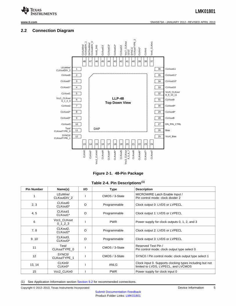
2.2 Connection Diagram
Figure 2-1. 48-Pin Package
Table 2-4. Pin Descriptions (1)
Pin Number Name(s) I/O Type Description
LEuWire/ MICROWIRE Latch Enable Input /1 I CMOS / 3-StateCLKoutDIV_2 Pin control mode: clock divider 2
CLKout02, 3 O Programmable Clock output 0: LVDS or LVPECLCLKout0*
CLKout14, 5 O Programmable Clock output 1: LVDS or LVPECLCLKout1*
Vcc1_CLKout6 I PWR Power supply for clock outputs 0, 1, 2, and 30_1_2_3
CLKout2,7, 8 O Programmable Clock output 2: LVDS or LVPECLCLKout2*
CLKout3,9. 10 O Programmable Clock output 3: LVDS or LVPECLCLKout3*
Test/ Reserved Test Pin /11 I CMOS / 3-StateCLKoutTYPE_0 Pin control mode: clock output type select 0
SYNC0/12 I CMOS / 3-State SYNC0 / Pin control mode: clock output type select 1CLKoutTYPE_1
CLKin0/ Clock input 0. Supports clocking types including but not13, 14 I ANLGCLKin0* limited to LVDS, LVPECL, and LVCMOS
15 Vcc2_CLKin0 I PWR Power supply for clock input 0
(1) See Application Information section Section 9.2 for recommended connections.
Copyright © 2012–2013, Texas Instruments Incorporated Device Information 5Submit Documentation FeedbackProduct Folder Links: LMK01801
LMK01801
SNAS573A –JANUARY 2012–REVISED APRIL 2013 www.ti.com
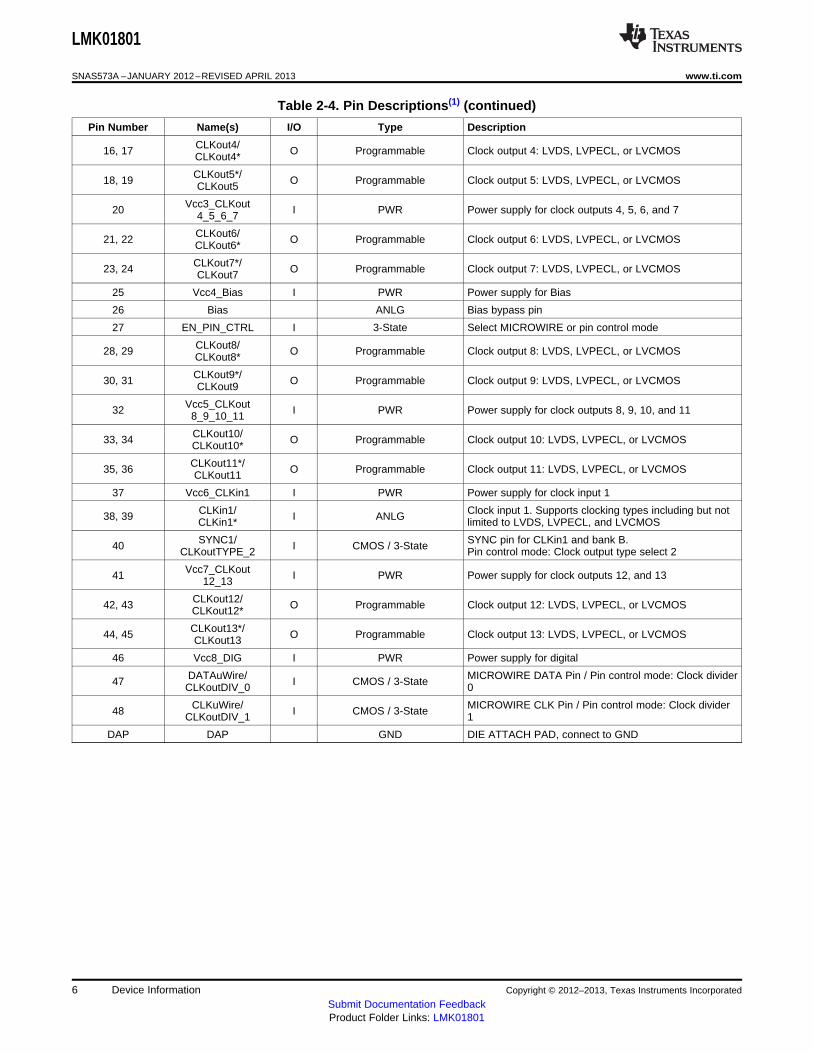
Table 2-4. Pin Descriptions(1) (continued)
Pin Number Name(s) I/O Type Description
CLKout4/16, 17 O Programmable Clock output 4: LVDS, LVPECL, or LVCMOSCLKout4*
CLKout5*/18, 19 O Programmable Clock output 5: LVDS, LVPECL, or LVCMOSCLKout5
Vcc3_CLKout20 I PWR Power supply for clock outputs 4, 5, 6, and 74_5_6_7
CLKout6/21, 22 O Programmable Clock output 6: LVDS, LVPECL, or LVCMOSCLKout6*
CLKout7*/23, 24 O Programmable Clock output 7: LVDS, LVPECL, or LVCMOSCLKout7
25 Vcc4_Bias I PWR Power supply for Bias
26 Bias ANLG Bias bypass pin
27 EN_PIN_CTRL I 3-State Select MICROWIRE or pin control mode
CLKout8/28, 29 O Programmable Clock output 8: LVDS, LVPECL, or LVCMOSCLKout8*
CLKout9*/30, 31 O Programmable Clock output 9: LVDS, LVPECL, or LVCMOSCLKout9
Vcc5_CLKout32 I PWR Power supply for clock outputs 8, 9, 10, and 118_9_10_11
CLKout10/33, 34 O Programmable Clock output 10: LVDS, LVPECL, or LVCMOSCLKout10*
CLKout11*/35, 36 O Programmable Clock output 11: LVDS, LVPECL, or LVCMOSCLKout11
37 Vcc6_CLKin1 I PWR Power supply for clock input 1
CLKin1/ Clock input 1. Supports clocking types including but not38, 39 I ANLGCLKin1* limited to LVDS, LVPECL, and LVCMOS
SYNC1/ SYNC pin for CLKin1 and bank B.40 I CMOS / 3-StateCLKoutTYPE_2 Pin control mode: Clock output type select 2
Vcc7_CLKout41 I PWR Power supply for clock outputs 12, and 1312_13
CLKout12/42, 43 O Programmable Clock output 12: LVDS, LVPECL, or LVCMOSCLKout12*
CLKout13*/44, 45 O Programmable Clock output 13: LVDS, LVPECL, or LVCMOSCLKout13
46 Vcc8_DIG I PWR Power supply for digital
DATAuWire/ MICROWIRE DATA Pin / Pin control mode: Clock divider47 I CMOS / 3-StateCLKoutDIV_0 0
CLKuWire/ MICROWIRE CLK Pin / Pin control mode: Clock divider48 I CMOS / 3-StateCLKoutDIV_1 1
DAP DAP GND DIE ATTACH PAD, connect to GND
6 Device Information Copyright © 2012–2013, Texas Instruments Incorporated
Submit Documentation FeedbackProduct Folder Links: LMK01801
LMK01801
www.ti.com SNAS573A –JANUARY 2012–REVISED APRIL 2013
These devices have limited built-in ESD protection. The leads should be shorted together or the device placed in conductive foamduring storage or handling to prevent electrostatic damage to the MOS gates.
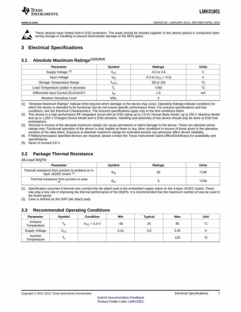
3 Electrical Specifications
3.1 Absolute Maximum Ratings (1) (2) (3) (4)
Parameter Symbol Ratings Units
Supply Voltage (5) VCC -0.3 to 3.6 V
Input Voltage VIN -0.3 to (VCC + 0.3) V
Storage Temperature Range TSTG -65 to 150 °C
Lead Temperature (solder 4 seconds) TL +260 °C
Differential Input Current (CLKinX/X*) IIN ± 5 mA
Moisture Sensitivty Level MSL 3
(1) "Absolute Maximum Ratings" indicate limits beyond which damage to the device may occur. Operating Ratings indicate conditions forwhich the device is intended to be functional, but do not ensure specific performance limits. For ensured specifications and testconditions, see the Electrical Characteristics. The ensured specifications apply only to the test conditions listed.
(2) This device is a high performance RF integrated circuit with an ESD rating up to 2.5 kV Human Body Model, up to 250 V Machine Modeland up to 1,250 V Charged Device Model and is ESD sensitive. Handling and assembly of this device should only be done at ESD-freeworkstations.
(3) Stresses in excess of the absolute maximum ratings can cause permanent or latent damage to the device. These are absolute stressratings only. Functional operation of the device is only implied at these or any other conditions in excess of those given in the operationsections of the data sheet. Exposure to absolute maximum ratings for extended periods can adversely affect device reliability.
(4) If Military/Aerospace specified devices are required, please contact the Texas Instruments Sales Office/Distributors for availability andspecifications.
(5) Never to exceed 3.6 V.
3.2 Package Thermal Resistance48-Lead WQFN
Parameter Symbol Ratings Units
Thermal resistance from junction to ambient on 4- θJA 26 °C/Wlayer JEDEC board (1)
Thermal resistance from junction to case θJC 3 °C/W(2)
(1) Specification assumes 9 thermal vias connect the die attach pad to the embedded copper plane on the 4-layer JEDEC board. Thesevias play a key role in improving the thermal performance of the WQFN. It is recommended that the maximum number of vias be used inthe board layout.
(2) Case is defined as the DAP (die attach pad).
3.3 Recommended Operating ConditionsParameter Symbol Condition Min Typical Max Unit
Ambient TA VCC = 3.3 V -40 25 85 °CTemperature
Supply Voltage VCC 3.15 3.3 3.45 V
Junction TJ 125 °CTemperature
Copyright © 2012–2013, Texas Instruments Incorporated Electrical Specifications 7Submit Documentation FeedbackProduct Folder Links: LMK01801
LMK01801
SNAS573A –JANUARY 2012–REVISED APRIL 2013 www.ti.com
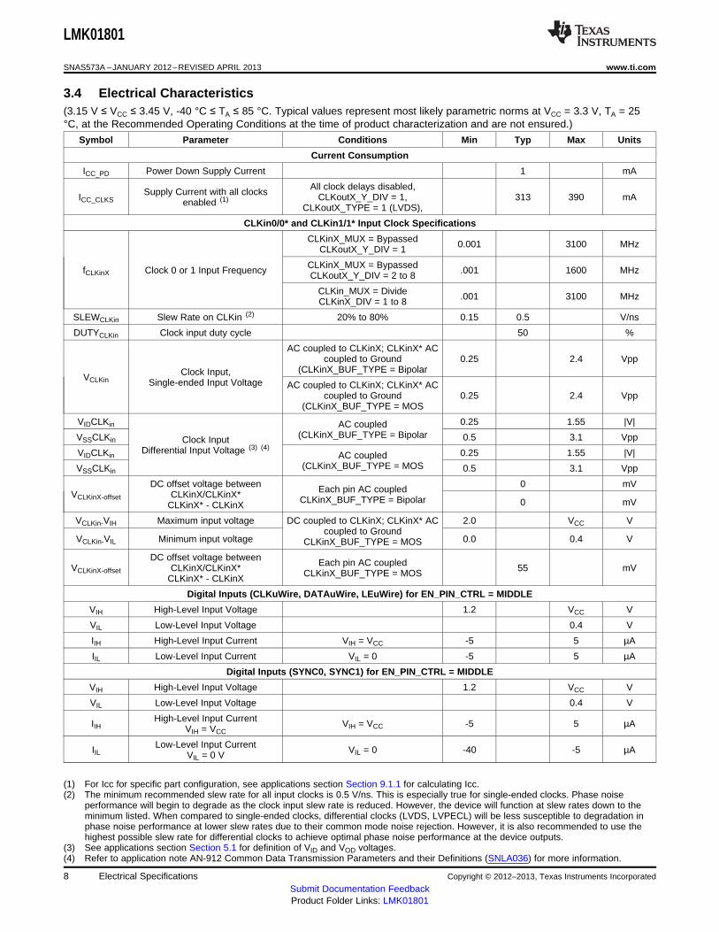
3.4 Electrical Characteristics(3.15 V ≤ VCC ≤ 3.45 V, -40 °C ≤ TA ≤ 85 °C. Typical values represent most likely parametric norms at VCC = 3.3 V, TA = 25°C, at the Recommended Operating Conditions at the time of product characterization and are not ensured.)
Symbol Parameter Conditions Min Typ Max Units
Current Consumption
ICC_PD Power Down Supply Current 1 mA
All clock delays disabled,Supply Current with all clocksICC_CLKS CLKoutX_Y_DIV = 1, 313 390 mAenabled (1)CLKoutX_TYPE = 1 (LVDS),
CLKin0/0* and CLKin1/1* Input Clock Specifications
CLKinX_MUX = Bypassed 0.001 3100 MHzCLKoutX_Y_DIV = 1
CLKinX_MUX = BypassedfCLKinX Clock 0 or 1 Input Frequency .001 1600 MHzCLKoutX_Y_DIV = 2 to 8
CLKin_MUX = Divide .001 3100 MHzCLKinX_DIV = 1 to 8
SLEWCLKin Slew Rate on CLKin (2) 20% to 80% 0.15 0.5 V/ns
DUTYCLKin Clock input duty cycle 50 %
AC coupled to CLKinX; CLKinX* ACcoupled to Ground 0.25 2.4 Vpp
(CLKinX_BUF_TYPE = BipolarClock Input,VCLKin Single-ended Input Voltage AC coupled to CLKinX; CLKinX* ACcoupled to Ground 0.25 2.4 Vpp
(CLKinX_BUF_TYPE = MOS
VIDCLKin 0.25 1.55 |V|AC coupled(CLKinX_BUF_TYPE = BipolarVSSCLKin 0.5 3.1 VppClock Input
Differential Input Voltage (3) (4)VIDCLKin 0.25 1.55 |V|AC coupled
(CLKinX_BUF_TYPE = MOSVSSCLKin 0.5 3.1 Vpp
DC offset voltage between 0 mVEach pin AC coupledVCLKinX-offset CLKinX/CLKinX* CLKinX_BUF_TYPE = Bipolar 0 mVCLKinX* - CLKinX
VCLKin-VIH Maximum input voltage DC coupled to CLKinX; CLKinX* AC 2.0 VCC Vcoupled to Ground
VCLKin-VIL Minimum input voltage 0.0 0.4 VCLKinX_BUF_TYPE = MOS
DC offset voltage between Each pin AC coupledVCLKinX-offset CLKinX/CLKinX* 55 mVCLKinX_BUF_TYPE = MOSCLKinX* - CLKinX
Digital Inputs (CLKuWire, DATAuWire, LEuWire) for EN_PIN_CTRL = MIDDLE
VIH High-Level Input Voltage 1.2 VCC V
VIL Low-Level Input Voltage 0.4 V
IIH High-Level Input Current VIH = VCC -5 5 µA
IIL Low-Level Input Current VIL = 0 -5 5 µA
Digital Inputs (SYNC0, SYNC1) for EN_PIN_CTRL = MIDDLE
VIH High-Level Input Voltage 1.2 VCC V
VIL Low-Level Input Voltage 0.4 V
High-Level Input CurrentIIH VIH = VCC -5 5 µAVIH = VCC
Low-Level Input CurrentIIL VIL = 0 -40 -5 µAVIL = 0 V
(1) For Icc for specific part configuration, see applications section Section 9.1.1 for calculating Icc.(2) The minimum recommended slew rate for all input clocks is 0.5 V/ns. This is especially true for single-ended clocks. Phase noise
performance will begin to degrade as the clock input slew rate is reduced. However, the device will function at slew rates down to theminimum listed. When compared to single-ended clocks, differential clocks (LVDS, LVPECL) will be less susceptible to degradation inphase noise performance at lower slew rates due to their common mode noise rejection. However, it is also recommended to use thehighest possible slew rate for differential clocks to achieve optimal phase noise performance at the device outputs.
(3) See applications section Section 5.1 for definition of VID and VOD voltages.(4) Refer to application note AN-912 Common Data Transmission Parameters and their Definitions (SNLA036) for more information.
8 Electrical Specifications Copyright © 2012–2013, Texas Instruments Incorporated
Submit Documentation FeedbackProduct Folder Links: LMK01801
LMK01801
www.ti.com SNAS573A –JANUARY 2012–REVISED APRIL 2013
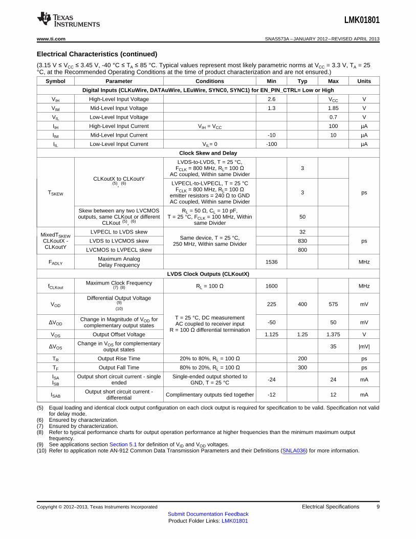
Electrical Characteristics (continued)
(3.15 V ≤ VCC ≤ 3.45 V, -40 °C ≤ TA ≤ 85 °C. Typical values represent most likely parametric norms at VCC = 3.3 V, TA = 25°C, at the Recommended Operating Conditions at the time of product characterization and are not ensured.)
Symbol Parameter Conditions Min Typ Max Units
Digital Inputs (CLKuWire, DATAuWire, LEuWire, SYNC0, SYNC1) for EN_PIN_CTRL= Low or High
VIH High-Level Input Voltage 2.6 VCC V
VIM Mid-Level Input Voltage 1.3 1.85 V
VIL Low-Level Input Voltage 0.7 V
IIH High-Level Input Current VIH = VCC 100 µA
IIM Mid-Level Input Current -10 10 µA
IIL Low-Level Input Current VIL= 0 -100 µA
Clock Skew and Delay
LVDS-to-LVDS, T = 25 °C,FCLK = 800 MHz, RL= 100 Ω 3
AC coupled, Within same DividerCLKoutX to CLKoutY
LVPECL-to-LVPECL, T = 25 °C(5), (6)
FCLK = 800 MHz, RL= 100 ΩTSKEW 3 psemitter resistors = 240 Ω to GNDAC coupled, Within same Divider
Skew between any two LVCMOS RL = 50 Ω, CL = 10 pF,outputs, same CLKout or different T = 25 °C, FCLK = 100 MHz, Within 50
CLKout (5), (6) same Divider
LVPECL to LVDS skew 32MixedTSKEW Same device, T = 25 °C,CLKoutX - LVDS to LVCMOS skew 830 ps250 MHz, Within same DividerCLKoutY LVCMOS to LVPECL skew 800
Maximum AnalogFADLY 1536 MHzDelay Frequency
LVDS Clock Outputs (CLKoutX)
Maximum Clock FrequencyfCLKout RL = 100 Ω 1600 MHz(7) (8)
Differential Output VoltageVOD
(9) 225 400 575 mV(10)
T = 25 °C, DC measurementChange in Magnitude of VOD forΔVOD -50 50 mVAC coupled to receiver inputcomplementary output statesR = 100 Ω differential termination
VOS Output Offset Voltage 1.125 1.25 1.375 V
Change in VOS for complementaryΔVOS 35 |mV|output states
TR Output Rise Time 20% to 80%, RL = 100 Ω 200 ps
TF Output Fall Time 80% to 20%, RL = 100 Ω 300 ps
ISA Output short circuit current - single Single-ended output shorted to -24 24 mAISB ended GND, T = 25 °C
Output short circuit current -ISAB Complimentary outputs tied together -12 12 mAdifferential
(5) Equal loading and identical clock output configuration on each clock output is required for specification to be valid. Specification not validfor delay mode.
(6) Ensured by characterization.(7) Ensured by characterization.(8) Refer to typical performance charts for output operation performance at higher frequencies than the minimum maximum output
frequency.(9) See applications section Section 5.1 for definition of VID and VOD voltages.(10) Refer to application note AN-912 Common Data Transmission Parameters and their Definitions (SNLA036) for more information.
Copyright © 2012–2013, Texas Instruments Incorporated Electrical Specifications 9Submit Documentation FeedbackProduct Folder Links: LMK01801
LMK01801
SNAS573A –JANUARY 2012–REVISED APRIL 2013 www.ti.com
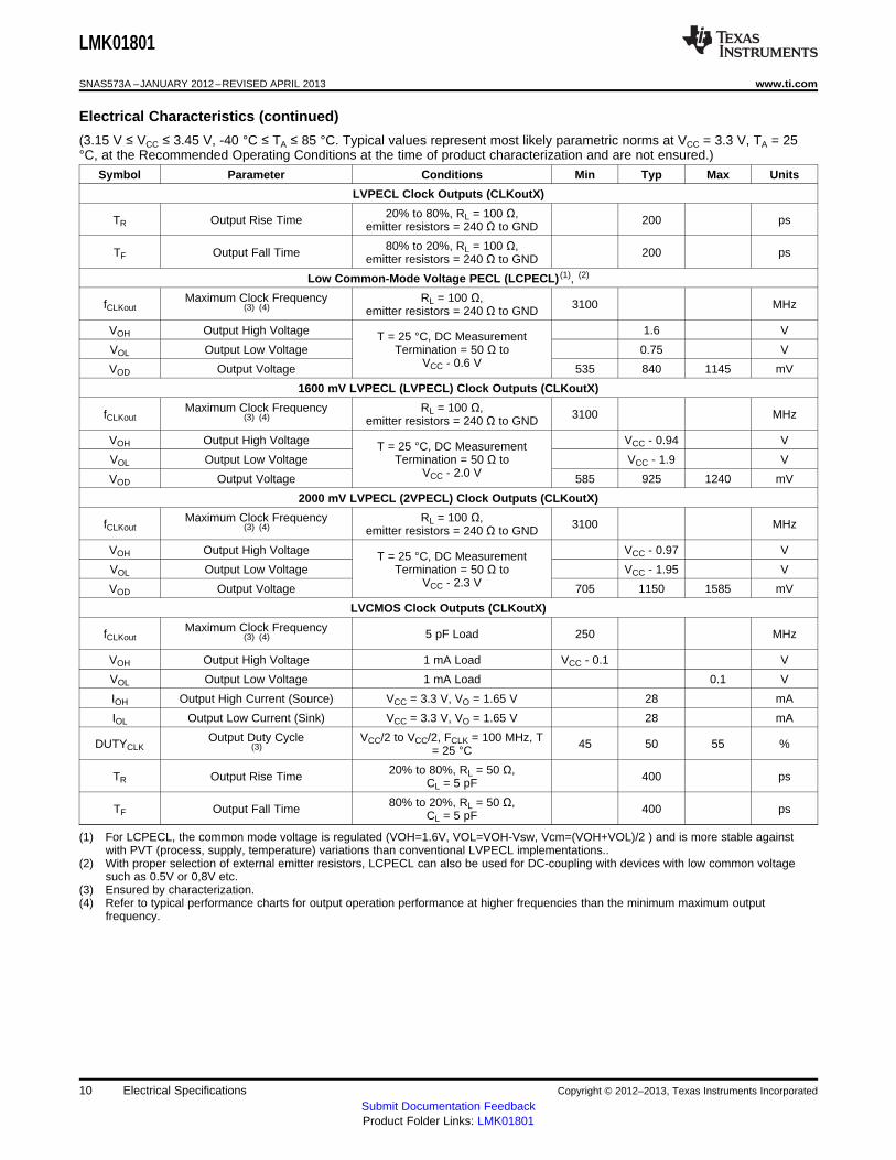
Electrical Characteristics (continued)
(3.15 V ≤ VCC ≤ 3.45 V, -40 °C ≤ TA ≤ 85 °C. Typical values represent most likely parametric norms at VCC = 3.3 V, TA = 25°C, at the Recommended Operating Conditions at the time of product characterization and are not ensured.)
Symbol Parameter Conditions Min Typ Max Units
LVPECL Clock Outputs (CLKoutX)
20% to 80%, RL = 100 Ω,TR Output Rise Time 200 psemitter resistors = 240 Ω to GND
80% to 20%, RL = 100 Ω,TF Output Fall Time 200 psemitter resistors = 240 Ω to GND
Low Common-Mode Voltage PECL (LCPECL) (1), (2)
Maximum Clock Frequency RL = 100 Ω,fCLKout 3100 MHz(3) (4) emitter resistors = 240 Ω to GND
VOH Output High Voltage 1.6 VT = 25 °C, DC MeasurementVOL Output Low Voltage Termination = 50 Ω to 0.75 V
VCC - 0.6 VVOD Output Voltage 535 840 1145 mV
1600 mV LVPECL (LVPECL) Clock Outputs (CLKoutX)
Maximum Clock Frequency RL = 100 Ω,fCLKout 3100 MHz(3) (4) emitter resistors = 240 Ω to GND
VOH Output High Voltage VCC - 0.94 VT = 25 °C, DC MeasurementVOL Output Low Voltage Termination = 50 Ω to VCC - 1.9 V
VCC - 2.0 VVOD Output Voltage 585 925 1240 mV
2000 mV LVPECL (2VPECL) Clock Outputs (CLKoutX)
Maximum Clock Frequency RL = 100 Ω,fCLKout 3100 MHz(3) (4) emitter resistors = 240 Ω to GND
VOH Output High Voltage VCC - 0.97 VT = 25 °C, DC MeasurementVOL Output Low Voltage Termination = 50 Ω to VCC - 1.95 V
VCC - 2.3 VVOD Output Voltage 705 1150 1585 mV
LVCMOS Clock Outputs (CLKoutX)
Maximum Clock FrequencyfCLKout 5 pF Load 250 MHz(3) (4)
VOH Output High Voltage 1 mA Load VCC - 0.1 V
VOL Output Low Voltage 1 mA Load 0.1 V
IOH Output High Current (Source) VCC = 3.3 V, VO = 1.65 V 28 mA
IOL Output Low Current (Sink) VCC = 3.3 V, VO = 1.65 V 28 mA
Output Duty Cycle VCC/2 to VCC/2, FCLK = 100 MHz, TDUTYCLK 45 50 55 %(3) = 25 °C
20% to 80%, RL = 50 Ω,TR Output Rise Time 400 psCL = 5 pF
80% to 20%, RL = 50 Ω,TF Output Fall Time 400 psCL = 5 pF
(1) For LCPECL, the common mode voltage is regulated (VOH=1.6V, VOL=VOH-Vsw, Vcm=(VOH+VOL)/2 ) and is more stable againstwith PVT (process, supply, temperature) variations than conventional LVPECL implementations..
(2) With proper selection of external emitter resistors, LCPECL can also be used for DC-coupling with devices with low common voltagesuch as 0.5V or 0,8V etc.
(3) Ensured by characterization.(4) Refer to typical performance charts for output operation performance at higher frequencies than the minimum maximum output
frequency.
10 Electrical Specifications Copyright © 2012–2013, Texas Instruments Incorporated
Submit Documentation FeedbackProduct Folder Links: LMK01801

tDCS
D26 D25 D24 D23
tCDHtCWH tCWL
D22 D0 A4 A1 A0
MSB LSB
DATAuWire
CLKuWire
LEuWire
tCES
tEWH
tECS
LMK01801
www.ti.com SNAS573A –JANUARY 2012–REVISED APRIL 2013
Electrical Characteristics (continued)
(3.15 V ≤ VCC ≤ 3.45 V, -40 °C ≤ TA ≤ 85 °C. Typical values represent most likely parametric norms at VCC = 3.3 V, TA = 25°C, at the Recommended Operating Conditions at the time of product characterization and are not ensured.)
Symbol Parameter Conditions Min Typ Max Units
MICROWIRE Interface Timing
TECS LE to Clock Set Up Time See MICROWIRE Input Timing 25 ns
TDCS Data to Clock Set Up Time See MICROWIRE Input Timing 25 ns
TCDH Clock to Data Hold Time See MICROWIRE Input Timing 8 ns
TCWH Clock Pulse Width High See MICROWIRE Input Timing 25 ns
TCWL Clock Pulse Width Low See MICROWIRE Input Timing 25 ns
TCES Clock to LE Set Up Time See MICROWIRE Input Timing 25 ns
TEWH LE Pulse Width See MICROWIRE Input Timing 25 ns
TCR Falling Clock to Readback Time See MICROWIRE Readback Timing 25 ns
3.5 Serial MICROWIRE Timing Diagram
Figure 3-1. MICROWIRE Timing Diagram
Register programming information on the DATAuWire pin is clocked into a shift register on each risingedge of the CLKuWire signal. On the rising edge of the LEuWire signal, the register is sent from the shiftregister to the register addressed. A slew rate of at least 30 V/µs is recommended for these signals. Afterprogramming is complete the CLKuWire, DATAuWire, and LEuWire signals should be returned to a lowstate.
Copyright © 2012–2013, Texas Instruments Incorporated Electrical Specifications 11Submit Documentation FeedbackProduct Folder Links: LMK01801
10 100 1k 10k
-180
-175
-170
-165
-160
-155
-150
-145
-140
NO
ISE
FLO
OR
(dB
c/H
z)
FREQUENCY (MHz)
LVPECL (differential)Re=240
LVPECL (differential)Re=120
10 100 1k 10k
-180
-175
-170
-165
-160
-155
-150
-145
NO
ISE
FLO
OR
(dB
c/H
z)
FREQUENCY (MHz)
LVDS (differential)
LVCMOS
0 100 200 300 400 500
0.0
0.5
1.0
1.5
2.0
2.5
3.0
3.5
4.0
SIN
GLE
EN
DE
D P
-P V
OLT
AG
E (
V)
FREQUENCY (MHz)
22 pF Load
10 pF Load
5 pF Load
0 50 100 150 200 250 300 350 400
0
20
40
60
80
ICC
(m
A)
FREQUENCY (MHz)
0 400 800 1200 1600 2000
0.0
0.2
0.4
0.6
0.8
1.0
DIF
FE
RE
NT
IAL
P-P
VO
LTA
GE
(V
)
FREQUENCY (MHz)0 500 1000 1500 2000 2500 3000
0.0
0.5
1.0
1.5
2.0
DIF
FE
RE
NT
IAL
P-P
VO
LTA
GE
(V
)
FREQUENCY (MHz)
LVPECL 2V Mode
LVPECL 1.6V Mode
LCPECL Mode
LMK01801
SNAS573A –JANUARY 2012–REVISED APRIL 2013 www.ti.com
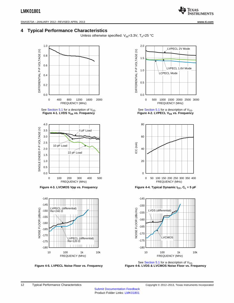
4 Typical Performance CharacteristicsUnless otherwise specified: Vdd=3.3V, TA=25 °C
See Section 5.1 for a description of VSS. See Section 5.1 for a description of VSS.Figure 4-1. LVDS VSS vs. Frequency Figure 4-2. LVPECL VSS vs. Frequency
Figure 4-3. LVCMOS Vpp vs. Frequency Figure 4-4. Typical Dynamic ICC, CL = 5 pF
See Section 5.1 for a description of VSS.Figure 4-5. LVPECL Noise Floor vs. Frequency Figure 4-6. LVDS & LVCMOS Noise Floor vs. Frequency
12 Typical Performance Characteristics Copyright © 2012–2013, Texas Instruments Incorporated
Submit Documentation FeedbackProduct Folder Links: LMK01801
VA
VB
GND
VOD = | VA - VB | VSS = 2·VOD
VOD Definition VSS Definition for Output
Non-Inverting Clock
Inverting Clock
VOD 2·VOD
VA
VB
GND
VID = | VA - VB | VSS = 2·VID
VID Definition VSS Definition for Input
Non-Inverting Clock
Inverting Clock
VID 2·VID
LMK01801
www.ti.com SNAS573A –JANUARY 2012–REVISED APRIL 2013
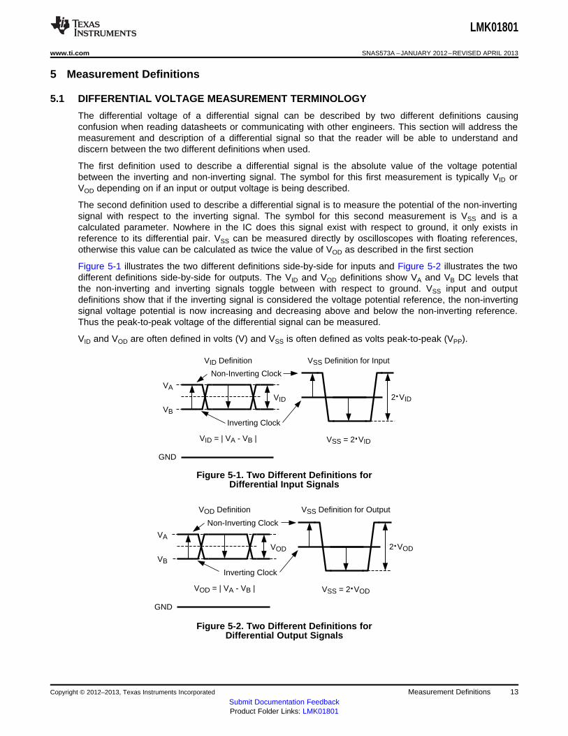
5 Measurement Definitions
5.1 DIFFERENTIAL VOLTAGE MEASUREMENT TERMINOLOGY
The differential voltage of a differential signal can be described by two different definitions causingconfusion when reading datasheets or communicating with other engineers. This section will address themeasurement and description of a differential signal so that the reader will be able to understand anddiscern between the two different definitions when used.
The first definition used to describe a differential signal is the absolute value of the voltage potentialbetween the inverting and non-inverting signal. The symbol for this first measurement is typically VID orVOD depending on if an input or output voltage is being described.
The second definition used to describe a differential signal is to measure the potential of the non-invertingsignal with respect to the inverting signal. The symbol for this second measurement is VSS and is acalculated parameter. Nowhere in the IC does this signal exist with respect to ground, it only exists inreference to its differential pair. VSS can be measured directly by oscilloscopes with floating references,otherwise this value can be calculated as twice the value of VOD as described in the first section
Figure 5-1 illustrates the two different definitions side-by-side for inputs and Figure 5-2 illustrates the twodifferent definitions side-by-side for outputs. The VID and VOD definitions show VA and VB DC levels thatthe non-inverting and inverting signals toggle between with respect to ground. VSS input and outputdefinitions show that if the inverting signal is considered the voltage potential reference, the non-invertingsignal voltage potential is now increasing and decreasing above and below the non-inverting reference.Thus the peak-to-peak voltage of the differential signal can be measured.
VID and VOD are often defined in volts (V) and VSS is often defined as volts peak-to-peak (VPP).
Figure 5-1. Two Different Definitions forDifferential Input Signals
Figure 5-2. Two Different Definitions forDifferential Output Signals
Copyright © 2012–2013, Texas Instruments Incorporated Measurement Definitions 13Submit Documentation FeedbackProduct Folder Links: LMK01801
LMK01801
SNAS573A –JANUARY 2012–REVISED APRIL 2013 www.ti.com
6 Features
6.1 SYSTEM ARCHITECTURE
The LMK01801 is a dual clock buffer which allows separate clock domains on the same IC with options todivide and delay signals.
The LMK01801 consists of two separate buffer banks, each with its own input divider, output dividers andprogrammable control of clock output channels.• Bank A has two clock output groups, see the Section 2.1 for more details.• Bank B has two clock output groups, one of which has analog and digital delay. See the Section 2.1 for
more details.
Each bank has it own common input divider and is then divided into output groups which share an outputdivider.
The LMK01801 comes in a 48-pin WQFN package.
6.2 HIGH SPEED CLOCK INPUTS (CLKin0/CLKin0* and CLKin1/CLKin1*)
The LMK01801 has two clock inputs, CLKin0 and CLKin1 which can be driven differentially or single-ended. See Section 9.4 for more information. Each input has a 2 to 8 divider that may be enabled orbypassed.
6.3 CLOCK DISTRIBUTION
The LMK01801 features a total of 14 differential outputs. CLKout0 through CLKout7 are driven fromCLKin0 and CLKout8 through CLKout13 are driven from CLKin1.
6.4 SMALL DIVIDER (1 to 8)
There are three small dividers which drive CLKout0 to CLKout3, CLKout4 to CLKout7, and CLKout8 toCLKout 11. These dividers support a divide range of 1 to 8 (even and odd).
6.5 LARGE DIVIDER (1 to 1045 )
The divider for CLKout12 and CLKout13 supports a divide range of 1 to 1045 (even and odd). Whendivides of 26 or greater are used, the divider/delay block uses extended mode.
6.6 CLKout ANALOG DELAY
Clock outputs 12 and 13 include a fine (analog) delay for phase adjustment of the clock outputs.
The fine (analog) delay allows a nominal 25 ps step size and range from 0 to 475 ps of total delay.Enabling the analog delay adds a nominal 500 ps of delay in addition to the programmed value.
When adjusting analog delay, glitches may occur on the clock outputs being adjusted.
14 Features Copyright © 2012–2013, Texas Instruments Incorporated
Submit Documentation FeedbackProduct Folder Links: LMK01801
LMK01801
www.ti.com SNAS573A –JANUARY 2012–REVISED APRIL 2013
6.7 CLKout12 & CLKout13 DIGITAL DELAY
CLKout12 and CLKout13 includes a coarse (digital) delay for phase adjustment of the clock outputs.
The coarse (digital) delay allows a group of outputs to be delayed by 4.5 to 12 clock distribution pathcycles in normal mode, or from 12.5 to 522 clock cycles in extended mode. The delay step can be assmall as half the period of the clock distribution path by using the CLKout12_13_HS bit. e.g. 2 GHz clockfrequency without using CLKin1 input clock divider results in 250 ps coarse tuning steps.
The coarse (digital) delay value takes effect on the clock outputs after a SYNC event.
There are 2 different ways to use the digital (coarse) delay.
1. Fixed Digital Delay
2. Relative Dynamic Digital Delay
These are further discussed in the Functional Description.
6.8 PROGRAMMABLE OUTPUTS
The outputs of the LMK01801 are programmable in a combination of output types based on Table 2-1.Programming the outputs is by MICROWIRE or by pin control mode based on the state of EN_PIN_CTRLpin.
Any LVPECL output type can be programmed to LCPECL, 1600, or 2000 mVpp amplitude levels. The2000 mVpp LVPECL output type is a Texas Instruments proprietary configuration that produces a 2000mVpp differential swing for compatibility with many data converters and is also known as 2VPECL.
6.9 CLOCK OUTPUT SYNCHRONIZATION
Using the SYNC input causes all active clock outputs to share a rising edge. See Section 7.6 for moreinformation.
The SYNC event also causes the digital delay value to take effect.
6.10 DEFAULT CLOCK OUTPUTS
The power on reset sets the device to operate with all outputs active in bypass mode (no divide) withLVDS output type. In this way the device can be used without programming for fan-out purposes.
Copyright © 2012–2013, Texas Instruments Incorporated Features 15Submit Documentation FeedbackProduct Folder Links: LMK01801
LMK01801
SNAS573A –JANUARY 2012–REVISED APRIL 2013 www.ti.com
7 Functional Description
7.1 PROGRAMMABLE MODE
When the EN_PIN_CTRL pin is floating (default by internal pull-up/pull-down) then programming is viaMICROWIRE.
See Table 2-1 for a description of available programming options for the LMK01801 in programmablemode.
7.2 PIN CONTROL MODE
The LMK01801 provides for an alternate function of the MICROWIRE (uWire) pins. This pin control modeis set by the logic of the EN_PIN_CTRL pin to provide limited control of the outputs and dividers.
When the EN_PIN_CTRL pin is set high or low (not open) then the output states can be programmed bypins, eliminating the need for an external FPGA or CPU.
If EN_PIN_CTRL is LOW then Table 2-2 in Section 2.1 defines how the outputs and dividers areconfigured.
If EN_PIN_CTRL is HIGH then Table 2-3 in Section 2.1 defines how the outputs and dividers areconfigured.
7.3 INPUTS / OUTPUTS
7.3.1 CLKin0 and CLKin1
There are two clock inputs CLKin0 and CLKin1. CLKin0 provides the input for output Bank A and CLKin1provides the input for the output Bank B. Each input has it's own divider (2 to 8) that may be bypassed.
7.4 INPUT AND OUTPUT DIVIDERS
This section discusses the recommended usage of input and output dividers.
Clock inputs 0 and 1 each have an associated divider (2 to 8) that may be enabled or bypassed.
Clock groups 1, 2 and 3 have small output dividers (1 to 8). Clock group 4 (CLKout12 and CLKout13) hasa large output divider (1 to 1045).
While the input and output clock dividers may be used in any combination the recommended operatingfrequency ranges are shown in the table below to minimize the phase noise floor:
Table 7-1. Input and Output Divider Input Frequency Ranges
Input Divider Output Divider Max Frequency
Bypassed Divide = 1 3.1 GHz
Bypassed Divide > 1 1.6 GHz
Divide = 2 to 8 Divide = 1 to 8 3.1 GHz
7.5 FIXED DIGITAL DELAY
This section discusses Fixed Digital Delay and associated registers.
Clock outputs 12 and 13 may be delayed relative to CLKout8 to CLKout 11 by up to 517.5 clockdistribution path periods if divide is 1 and 518.5 clock distribution path periods if divide is greater than 1.By programming a digital delay value from 4.5 to 522 clock distribution path periods, a relative clockoutput delay from 0 to 517.5 periods is achieved. The CLKout12_13_DDLY register sets the digital delayas shown in the table Table 7-2.
16 Functional Description Copyright © 2012–2013, Texas Instruments Incorporated
Submit Documentation FeedbackProduct Folder Links: LMK01801

LMK01801
www.ti.com SNAS573A –JANUARY 2012–REVISED APRIL 2013
Table 7-2. Possible Digital Delay Values
CLKout12_13_DDLY CLKout12_13_HS Digital Delay
5 1 4.5
5 0 5
6 1 5.5
6 0 6
7 1 6.5
7 0 7
... ... ...
520 0 520
521 1 520.5
521 0 521
522 1 521.5
522 0 522
The CLKout12_13_DDLY value only takes effect during a SYNC event and if theNO_SYNC_CLKout12_13 bit is cleared for this clock group. See Section 7.6 for more information.
The resolution of digital delay is related to the frequency at the input to the Clock Group 4 (CG4) clockdistribution path.
Digital Delay Resolution = 1 / (2 * Clock Frequency)
The digital delay between clock outputs can be dynamically adjusted with minimum or no disruption of theoutput clocks. See Section 7.6.1 for more information.
7.5.1 Fixed Digital Delay - Example
Given a CLKin1 clock frequency of 983.04 MHz as input to CG4, by using digital delay the outputs can beadjusted in 1 / (2 * 983.04 MHz) = ~509 ps steps (Assumes CLKin1_MUX = bypass).
To achieve a quadrature (90 degree) phase shift on 122.88 MHz outputs between CLKout12 andCLKout11 from a clock frequency of 983.04 MHz program:• Clock output divider to 8. CLKout8_11 = 8 and CLKout12_13_DIV = 8• Set clock digital delay value. CLKout12_13_DDLY = 5, CLKout12_13_HS = 0.
The frequency of 122.88 MHz has a period of ~8.14 ns. To delay 90 degrees of a 122.88 MHz clockperiod requires a ~2.03 ns delay. Given a digital delay step of ~509 ps, this requires a digital delay valueof 4 steps (2.03 ns / 509 ps = 4). Since the 4 steps are half period steps, CLKout12_13_DDLY isprogrammed 2 full periods beyond 5 for a total of 7.
Table 7-3 shows some of the possible phase delays in degrees achievable in the above example.
Table 7-3. Relative phase shift fromCLKout12 and CLKout13 to CLKout8 to CLKout11
CLKout12_13_DDLY CLKout12_13_HS Relative Digital Delay Degrees of 122.88 MHz
5 1 -0.5 -23°
5 0 0.0 0°
6 1 0.5 23°
6 0 1.0 45°
7 1 1.5 68°
7 0 2.0 90°
8 1 2.5 113°
8 0 3.0 135°
9 1 3.5 158°
Copyright © 2012–2013, Texas Instruments Incorporated Functional Description 17Submit Documentation FeedbackProduct Folder Links: LMK01801

LMK01801
SNAS573A –JANUARY 2012–REVISED APRIL 2013 www.ti.com
Table 7-3. Relative phase shift fromCLKout12 and CLKout13 to CLKout8 to CLKout11
(continued)
CLKout12_13_DDLY CLKout12_13_HS Relative Digital Delay Degrees of 122.88 MHz
9 0 4.0 180°
10 1 4.5 203°
10 0 5.0 225°
11 1 5.5 248°
11 0 6.0 270°
12 1 6.5 293°
12 0 7.0 315°
13 1 7.5 338°
13 0 8.0 360°
... ... ... ...
Figure 7-2 illustrates clock outputs programmed with different digital delay values during a SYNC event.
Refer to Section 7.6.1 for more information on dynamically adjusting digital delay.
7.6 CLOCK OUTPUT SYNCHRONIZATION (SYNC)
The purpose of the SYNC function is to synchronize the clock outputs with a fixed and known phaserelationship between each clock output selected for SYNC. SYNC can also be used to hold the outputs ina low or 0 state. The NO_SYNC_CLKoutX_Y bits can be set to disable synchronization for a clock group.
The digital delay value set by CLKout12_13_DDLY takes effect only upon a SYNC event. The digital delaydue to CLKout12_13_HS takes effect immediately upon programming. See Section 7.6.1 for moreinformation on dynamically changing digital delay.
It is necessary to ensure that the CLKin1 signal is stable before a sync event occurs whenCLKout12_13_DIV is greater than 1.
18 Functional Description Copyright © 2012–2013, Texas Instruments Incorporated
Submit Documentation FeedbackProduct Folder Links: LMK01801
LMK01801
www.ti.com SNAS573A –JANUARY 2012–REVISED APRIL 2013
Effect of SYNC
When SYNC is asserted, the outputs to be synchronized are held in a logic low state. When SYNC isunasserted, the clock outputs to be synchronized are activated and will transition to a high statesimultaneously with one another except where digital delay values have been programmed.
Refer to Section 7.6.1 for SYNC functionality when SYNC_QUAL = 1.
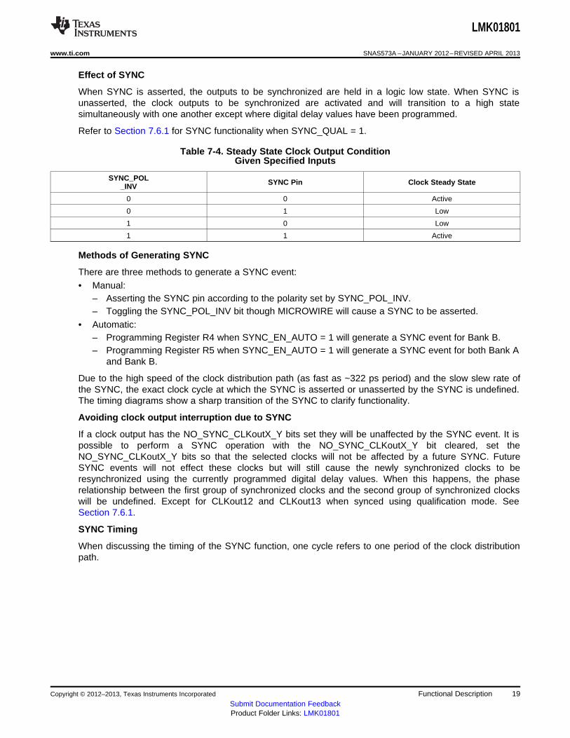
Table 7-4. Steady State Clock Output ConditionGiven Specified Inputs
SYNC_POL SYNC Pin Clock Steady State_INV
0 0 Active
0 1 Low
1 0 Low
1 1 Active
Methods of Generating SYNC
There are three methods to generate a SYNC event:• Manual:
– Asserting the SYNC pin according to the polarity set by SYNC_POL_INV.– Toggling the SYNC_POL_INV bit though MICROWIRE will cause a SYNC to be asserted.
• Automatic:– Programming Register R4 when SYNC_EN_AUTO = 1 will generate a SYNC event for Bank B.– Programming Register R5 when SYNC_EN_AUTO = 1 will generate a SYNC event for both Bank A
and Bank B.
Due to the high speed of the clock distribution path (as fast as ~322 ps period) and the slow slew rate ofthe SYNC, the exact clock cycle at which the SYNC is asserted or unasserted by the SYNC is undefined.The timing diagrams show a sharp transition of the SYNC to clarify functionality.
Avoiding clock output interruption due to SYNC
If a clock output has the NO_SYNC_CLKoutX_Y bits set they will be unaffected by the SYNC event. It ispossible to perform a SYNC operation with the NO_SYNC_CLKoutX_Y bit cleared, set theNO_SYNC_CLKoutX_Y bits so that the selected clocks will not be affected by a future SYNC. FutureSYNC events will not effect these clocks but will still cause the newly synchronized clocks to beresynchronized using the currently programmed digital delay values. When this happens, the phaserelationship between the first group of synchronized clocks and the second group of synchronized clockswill be undefined. Except for CLKout12 and CLKout13 when synced using qualification mode. SeeSection 7.6.1.
SYNC Timing
When discussing the timing of the SYNC function, one cycle refers to one period of the clock distributionpath.
Copyright © 2012–2013, Texas Instruments Incorporated Functional Description 19Submit Documentation FeedbackProduct Folder Links: LMK01801
5.5 cycles
4.5 cycles
CLKout0 to 11 ÷ 1
CLKout12 to 13 ÷ 2
5 cycles
CLKout12_13_DDLY & CLKout12_13_HS6 cycles
A B C D E F G
SYNC
CLKout12 to 13 ÷ 1
CLKout12_13_DDLY & CLKout12_13_HS
CLKinX
LMK01801
SNAS573A –JANUARY 2012–REVISED APRIL 2013 www.ti.com
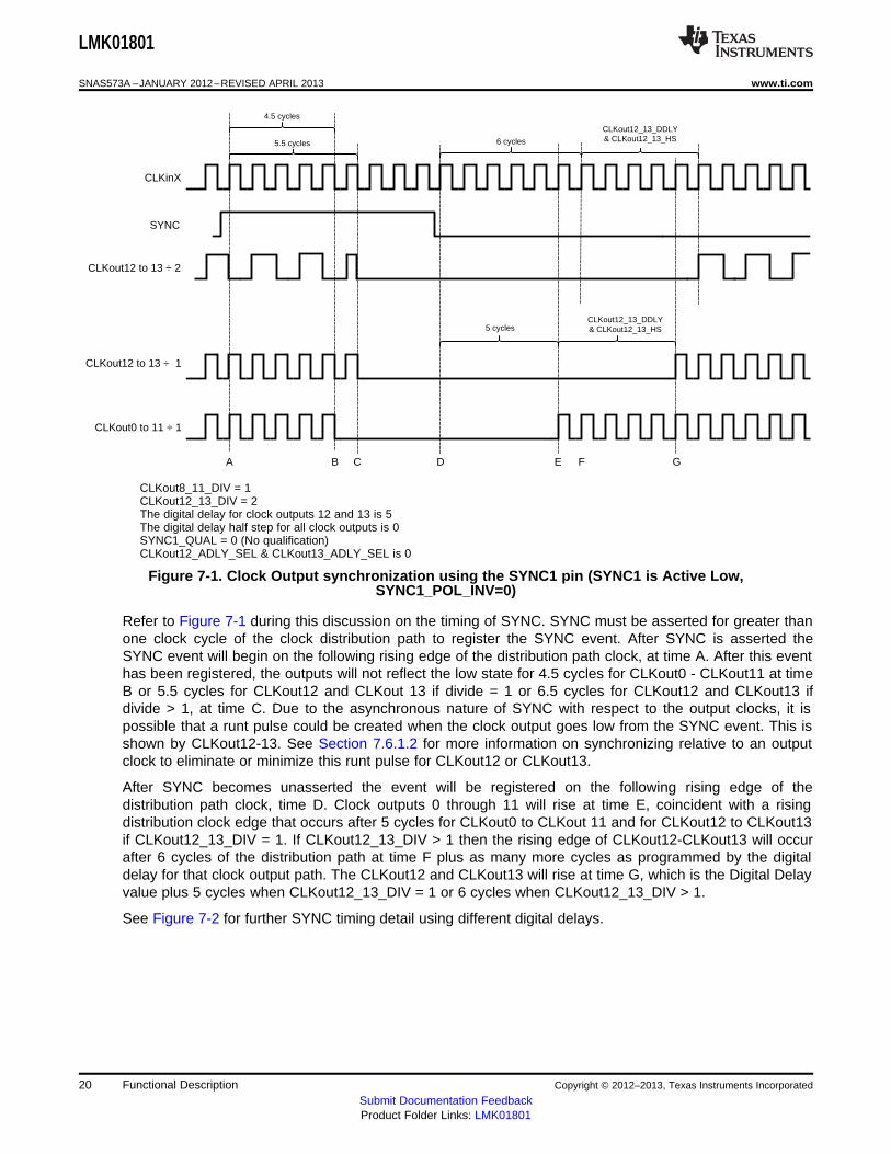
CLKout8_11_DIV = 1CLKout12_13_DIV = 2The digital delay for clock outputs 12 and 13 is 5The digital delay half step for all clock outputs is 0SYNC1_QUAL = 0 (No qualification)CLKout12_ADLY_SEL & CLKout13_ADLY_SEL is 0
Figure 7-1. Clock Output synchronization using the SYNC1 pin (SYNC1 is Active Low,SYNC1_POL_INV=0)
Refer to Figure 7-1 during this discussion on the timing of SYNC. SYNC must be asserted for greater thanone clock cycle of the clock distribution path to register the SYNC event. After SYNC is asserted theSYNC event will begin on the following rising edge of the distribution path clock, at time A. After this eventhas been registered, the outputs will not reflect the low state for 4.5 cycles for CLKout0 - CLKout11 at timeB or 5.5 cycles for CLKout12 and CLKout 13 if divide = 1 or 6.5 cycles for CLKout12 and CLKout13 ifdivide > 1, at time C. Due to the asynchronous nature of SYNC with respect to the output clocks, it ispossible that a runt pulse could be created when the clock output goes low from the SYNC event. This isshown by CLKout12-13. See Section 7.6.1.2 for more information on synchronizing relative to an outputclock to eliminate or minimize this runt pulse for CLKout12 or CLKout13.
After SYNC becomes unasserted the event will be registered on the following rising edge of thedistribution path clock, time D. Clock outputs 0 through 11 will rise at time E, coincident with a risingdistribution clock edge that occurs after 5 cycles for CLKout0 to CLKout 11 and for CLKout12 to CLKout13if CLKout12_13_DIV = 1. If CLKout12_13_DIV > 1 then the rising edge of CLKout12-CLKout13 will occurafter 6 cycles of the distribution path at time F plus as many more cycles as programmed by the digitaldelay for that clock output path. The CLKout12 and CLKout13 will rise at time G, which is the Digital Delayvalue plus 5 cycles when CLKout12_13_DIV = 1 or 6 cycles when CLKout12_13_DIV > 1.
See Figure 7-2 for further SYNC timing detail using different digital delays.
20 Functional Description Copyright © 2012–2013, Texas Instruments Incorporated
Submit Documentation FeedbackProduct Folder Links: LMK01801
5.5 cycles
Case 1: CLKout12
CLKout12_13_DDLY & CLKout12_13_HS6 cycles
A B C D E F
SYNC
Case 2: CLKout12
DistributionPath
4.5 cycles
Case 3: CLKout12
1 cycle2.5 cycles
LMK01801
www.ti.com SNAS573A –JANUARY 2012–REVISED APRIL 2013
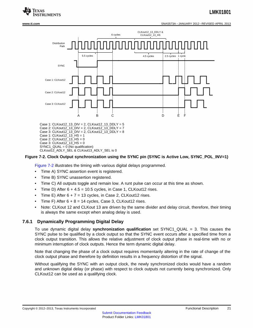
Case 1: CLKout12_13_DIV = 2, CLKout12_13_DDLY = 5Case 2: CLKout12_13_DIV = 2, CLKout12_13_DDLY = 7Case 3: CLKout12_13_DIV = 2, CLKout12_13_DDLY = 8Case 1: CLKout12_13_HS = 1Case 2: CLKout12_13_HS = 0Case 3: CLKout12_13_HS = 0SYNC1_QUAL = 0 (No qualification)CLKout12_ADLY_SEL & CLKout13_ADLY_SEL is 0
Figure 7-2. Clock Output synchronization using the SYNC pin (SYNC is Active Low, SYNC_POL_INV=1)
Figure 7-2 illustrates the timing with various digital delays programmed.• Time A) SYNC assertion event is registered.• Time B) SYNC unassertion registered.• Time C) All outputs toggle and remain low. A runt pulse can occur at this time as shown.• Time D) After 6 + 4.5 = 10.5 cycles, in Case 1, CLKout12 rises.• Time E) After 6 + 7 = 13 cycles, in Case 2, CLKout12 rises.• Time F) After 6 + 8 = 14 cycles, Case 3, CLKout12 rises.• Note: CLKout 12 and CLKout 13 are driven by the same divider and delay circuit, therefore, their timing
is always the same except when analog delay is used.
7.6.1 Dynamically Programming Digital Delay
To use dynamic digital delay synchronization qualification set SYNC1_QUAL = 3. This causes theSYNC pulse to be qualified by a clock output so that the SYNC event occurs after a specified time from aclock output transition. This allows the relative adjustment of clock output phase in real-time with no orminimum interruption of clock outputs. Hence the term dynamic digital delay.
Note that changing the phase of a clock output requires momentarily altering in the rate of change of theclock output phase and therefore by definition results in a frequency distortion of the signal.
Without qualifying the SYNC with an output clock, the newly synchronized clocks would have a randomand unknown digital delay (or phase) with respect to clock outputs not currently being synchronized. OnlyCLKout12 can be used as a qualifying clock.
Copyright © 2012–2013, Texas Instruments Incorporated Functional Description 21Submit Documentation FeedbackProduct Folder Links: LMK01801
LMK01801
SNAS573A –JANUARY 2012–REVISED APRIL 2013 www.ti.com
Relative Dynamic Digital Delay
When the qualifying clock digital delay is being adjusted, because the qualifying clock and the adjustedclock are the same, then a relative dynamic digital delay adjust is performed. Clocks withNO_SYNC_CLKoutX_Y = 1 are defined as clocks not being adjusted. These clocks operate withoutinterruption.
SYNC and Minimum Step Size
The minimum step size adjustment for digital delay is half a clock distribution path cycle. This is achievedby using the CLKout12_13_HS bit. The CLKout12_13_HS bit change effect is immediate without the needfor SYNC. To shift digital delay using CLKout12_13_DDLY, a SYNC signal must be generated for thechange to take effect.
Programming Overview
To dynamically adjust the digital delay with respect to an existing clock output the device should beprogrammed as follows:• Set SYNC1_QUAL = 3 for clock output qualification.• Set NO_SYNC_CLKout12_13 = 0 to enable synchronization on CLKout12 and CLKout13.• Set CLKout12_ADLY_SEL = 0.• Set NO_SYNC_CLKoutX_Y = 1 for the output clocks, except CLKout12 and CLKout13, that will
continue to operate during the SYNC event. There is no interruption of output on these clocks.• The SYNC_EN_AUTO bit may be set to cause a SYNC event to begin when register R4 is
programmed. The auto SYNC feature is a convenience since it does not require the application tomanually assert SYNC by toggling the SYNC_POL_INV bit or the SYNC pin when changing digitaldelay.
Internal Dynamic Digital Delay Timing
Once SYNC is qualified by an output clock, 1.5 cycles later an internal one shot pulse will occur. Thewidth of the one shot pulse is 3 cycles. This internal one shot pulse will cause the outputs to turn off andthen back on with a fixed delay with respect to the falling edge of the qualification clock. This allows fordynamic adjustments of digital delay with respect to an output clock.
The qualified SYNC timing is shown in Figure 7-3 for relative dynamic digital delay.
Dynamic Digital Delay Conditions
To perform a dynamic digital delay adjustment, the analog delay must be bypassed by settingCLKout12_ADLY_SEL to 0. If the analog delay is not bypassed the output synchronization may beinaccurate due to unknown analog delay settings.
When adjusting digital delay dynamically, the falling edge of the qualifying clock must coincide with thefalling edge of the clock distribution path. For this requirement to be met, program the CLKout12_13_HSvalue of the qualifying clock group according to Table 7-5.
Table 7-5. Half Step programming requirement ofqualifying clock during SYNC event
CLKout12_13_DIV value CLKout12_13_HS
Odd Must = 1 during SYNC event.
Even Must = 0 during SYNC event.
22 Functional Description Copyright © 2012–2013, Texas Instruments Incorporated
Submit Documentation FeedbackProduct Folder Links: LMK01801

LMK01801
www.ti.com SNAS573A –JANUARY 2012–REVISED APRIL 2013
7.6.1.1 RELATIVE DYNAMIC DIGITAL DELAY
Relative dynamic digital delay can be used to program a clock output to a specific phase offset fromanother clock output.
Pros:• Direct phase adjustment with respect to same clock output.• Possible glitch pulses from clock output will always be the same during digital delay adjustment
transient.Cons:
• For some clock divide values there may be a glitch pulse due to SYNC assertion.• Adjustments of digital delay requiring the half step bit (CLKout12_13_HS) for finer digital delay adjust
is complicated due to the half step requirement in Table 7-5 above.
7.6.1.2 RELATIVE DYNAMIC DIGITAL DELAY - EXAMPLE
To illustrate the relative dynamic digital delay adjust procedure, consider the following example.
System Requirements:• CLKin1 Frequency = 983.04 MHz• CLKout8 = 983.04 MHz (CLKout8_11_DIV = 1)• CLKout12 = 491.52 MHz (CLKout12_13_DIV = 2)• During initial programming:
– CLKout12_13_DDLY = 5– CLKout12_13_HS = 0– NO_SYNC_CLKoutX_Y = 0
The application requires the 491.52 MHz clock to be stepped in 90 degree steps (~508.6 ps), which is theminimum step resolution allowable by the clock distribution path. That is 1 / 983.04 MHz / 2 = ~169.5 ps.During the stepping of the 491.52 MHz clocks the 983.04 MHz clock must not be interrupted.
Step 1: The device is programmed from register R0 to R5 with values that result in the device operatingas desired, see the system requirements above. The phase of all the output clocks are aligned because allthe digital delay and half step values were the same when the SYNC was generated by programmingregister R5. The timing of this is as shown in Figure 7-1.
Step 2: Now the registers will be programmed to prepare for changing digital delay (or phase)dynamically.
Register Purpose
Use clock output for qualifying the SYNC pulse for dynamicallySYNC1_QUAL = 3 adjusting digital delay.
Clock output 8 (983.04 MHz) won't be affected by SYNC. It willNO_SYNC_CLKout7_11 = 1 operate without interruption.
Automatically generation of SYNC is not allowed because of the halfstep requirement.SYNC1_AUTO = 0 (default) SYNC must be generated manually by toggling the SYNC_POL_INVbit or the SYNC pin.
After the above registers have been programmed, the application may now dynamically adjust the digitaldelay of the 491.52 MHz clocks.
Step 3: Adjust digital delay of CLKout12 by one step.
Refer to Table 7-6 for the programming sequence to step one half clock distribution period forward orbackwards.
Copyright © 2012–2013, Texas Instruments Incorporated Functional Description 23Submit Documentation FeedbackProduct Folder Links: LMK01801

LMK01801
SNAS573A –JANUARY 2012–REVISED APRIL 2013 www.ti.com
Table 7-6. Programming sequence for one step adjust
Step direction and current HS state Programming Sequence
Adjust clock output one step forward. 1. CLKout12_13_HS = 1.CLKout12_13_HS = 0.
1. CLKout12_13_DDLY = 9.Adjust clock output one step forward. 2. Perform SYNC event.CLKout12_13_HS = 1. 3. CLKout12_13_HS = 0.
1. CLKout12_13_HS = 1.Adjust clock output one step backward. 2. CLKout12_13_DDLY = 5.CLKout12_13_HS = 0. 3. Perform SYNC event.
Adjust clock output one step backward. 1. CLKout12_13_HS = 0.CLKout12_13_HS = 1.
To fulfill the qualifying clock output half step requirement in Table 7-5 when dynamically adjusting digitaldelay, the CLKout12_13_HS bit must be set if CLKout12 or CLKout13 has an odd divide. So before anydynamic digital delay adjustment, CLKout12_13_HS must be set because the clock divide value is odd. Toachieve the final required digital delay adjustment, the CLKout12_13_HS bit may cleared after SYNC.
If a SYNC is to be generated this can be done by toggling the SYNC pin or by toggling theSYNC_POL_INV bit. Because of the internal one shot pulse, no strict timing of the SYNC pin orSYNC_POL_INV bit is required. After the SYNC event, the clock output will be at the specified phase. SeeFigure 7-3 for a detailed view of the timing diagram. The timing diagram critical points are:• Time A) SYNC assertion event is registered.• Time B) First qualifying falling clock output edge.• Time C) Second qualifying falling clock output edge.• Time D) Internal one shot pulse begins. 5.5 cycles later CLKout12 outputs will be forced low while 8.5
cycles later CLKout8 outputs will be forced low.• Time E) Internal one shot pulse ends. 6 cycles + digital delay cycles later CLKout12 or CLKout13
outputs rise. 10 cycles later CLKout8 to CLKout11 outputs rise.• Time F) CLKout12 to CLKout13 outputs are forced low.• Time G) Beginning of digital delay cycles.• Time H) CLKout8 to CLKout11 outputs are forced low.• Time I) CLKout8 to CLKout11 outputs rise now.• Time j) For CLKout12_13_DDLY = 5; the CLKout12 and CLKout13 outputs rise now.
24 Functional Description Copyright © 2012–2013, Texas Instruments Incorporated
Submit Documentation FeedbackProduct Folder Links: LMK01801

1.5 cycles
CLKout8 to 11, ÷ 2
CLKout12 to 13, ÷ 2HS = 1
CLKout12_13_DDLY & CLKout12_13_HS
A B C D E
CLKin1
Internal One Shot Pulse
1
3 cycles
H I
6 cycles
10.5 cycles
A B C D E F G J
6 cycles
2
8.5 cycles
LMK01801
www.ti.com SNAS573A –JANUARY 2012–REVISED APRIL 2013
(SYNC1_QUAL = 1, Qualify with clock output)Starting condition is after half step is removed (CLKout12_13_HS = 0).
Figure 7-3. Relative Dynamic Digital Delay Programming Example, 2nd adjust
Copyright © 2012–2013, Texas Instruments Incorporated Functional Description 25Submit Documentation FeedbackProduct Folder Links: LMK01801

LMK01801
SNAS573A –JANUARY 2012–REVISED APRIL 2013 www.ti.com
8 General Programming Information
LMK01801 devices are programmed using 32-bit registers. Each register consists of a 4-bit address fieldand 23-bit data field. The address field is formed by bits 0 through 3 (LSBs) and the data field is formed bybits 4 through 31 (MSBs). The contents of each register is clocked in MSB first (bit 31), and the LSB (bit 0)last. During programming, the LE signal should be held LOW. The serial data is clocked in on the risingedge of the CLK signal. After the LSB (bit 0) is clocked in the LE signal should be toggled LOW-to-HIGH-to-LOW to latch the contents into the register selected in the address field. It is recommended to programregisters in numeric order, for example R0 to R5 and R15 to achieve proper device operation. Figure 3-1illustrates the serial data timing sequence.
8.1 RECOMMENDED PROGRAMMING SEQUENCE
Registers are programmed in numeric order with R0 being the first and R15 being the last registerprogrammed. The recommended programming sequence involves programming R0 with the reset bit (b4)set to 1 to ensure the device is in a default state. Then R0 is programmed again, the reset bit is becleared to 0 during the re-programming of R0.
8.1.1 Overview• R0 (Init):
– Program R0 with RESET = 1. This ensures that the device is configured with default settings. WhenRESET =1, all other R0 bits are ignored.
• R0: Powerdown Controls and CLKin Dividers– Program R0 with RESET = 0
• R1 and R2: Clock output types• R3: SYNC Features and Analog Delay for CLKout12 and CLKout13• R4: Dynamic Digital Delay for CLKout12 and CLKout13• R5: CLKout Dividers and Analog Delay Select• R15: uWireLock
26 General Programming Information Copyright © 2012–2013, Texas Instruments Incorporated
Submit Documentation FeedbackProduct Folder Links: LMK01801

LMK01801
www.ti.com SNAS573A –JANUARY 2012–REVISED APRIL 2013
8.2 REGISTER MAP
Table 8-1 provides the register map for device programming:
Table 8-1. Register Map
Register 31 30 29 28 27 26 25 24 23 22 21 20 19 18 17 16 15 14 13 12 11 10 9 8 7 6 5 4 3 2 1 0
Data [31:4] Address [3:0]
CLKin1_ CLKin0_R0 0 1 0 0 1 0 0 0 CLKin1_DIV CLKin0_DIV 1 1 0 0 0 0MUX MUX
RE
SE
T
CLK
out4
_7_P
D
CLK
out0
_3_P
D
PO
WE
RD
OW
N
CLK
out8
_11_
PD
CLK
out1
2_13
_PD
CLK
in1_
BU
F_T
YP
E
CLK
in0_
BU
F_T
YP
E
CLKout3_ CLKout2_ CLKout1_ CLKout0_R1 CLKout7_TYPE CLKout6_TYPE CLKout5_TYPE CLKout4_TYPE 0 0 0 1TYPE TYPE TYPE TYPE
R2 0 0 0 0 CLKout13_TYPE CLKout12_TYPE CLKout11_TYPE CLKout10_TYPE CLKout9_TYPE CLKout8_TYPE 0 0 1 0
SYNC1_R3 0 0 0 1 0 0 1 1 0 CLKout12_13_ADLY 0 0 1 1QUAL
SY
NC
1_F
AS
T
SY
NC
0_F
AS
T
SY
NC
1_A
UT
O
SY
NC
0_A
UT
O
CLK
out1
2_13
_HS
SY
NC
1_P
OL_
INV
SY
NC
0_P
OL_
INV
NO
_SY
NC
_CLK
out4
_7
NO
_SY
NC
_CLK
out0
_3
NO
_SY
NC
_CLK
out8
_11
NO
_SY
NC
_CLK
out1
2_13
R4 0 0 0 0 0 0 0 0 0 0 0 0 0 0 0 0 0 0 CLKout12_13_DDLY 0 1 0 0
CLKout8_11 CLKout4_7 CLKout0_3R5 0 0 0 0 CLKout12_13_DIV 0 0 0 1 0 1_DIV _DIV _DIV
CLK
out1
3_A
DLY
_SE
L
CLK
out1
2_A
DLY
_SE
LR15 0 0 0 0 0 0 0 0 0 0 0 0 0 0 0 0 0 0 0 0 0 1 0 1 1 1 1 1 1 1 1
uWire
Lock
Copyright © 2012–2013, Texas Instruments Incorporated General Programming Information 27Submit Documentation FeedbackProduct Folder Links: LMK01801
LMK01801
SNAS573A –JANUARY 2012–REVISED APRIL 2013 www.ti.com
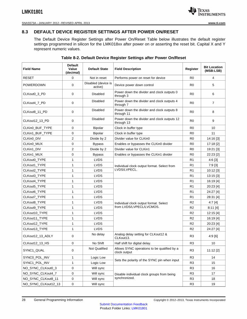
8.3 DEFAULT DEVICE REGISTER SETTINGS AFTER POWER ON/RESET
The Default Device Register Settings after Power On/Reset Table below illustrates the default registersettings programmed in silicon for the LMK018xx after power on or asserting the reset bit. Capital X and Yrepresent numeric values.
Table 8-2. Default Device Register Settings after Power On/Reset
Default Bit LocationField Name Value Default State Field Description Register (MSB:LSB)(decimal)
RESET 0 Not in reset Performs power on reset for device R0 4
Disabled (device isPOWERDOWN 0 Device power down control R0 5active)
Power down the divider and clock outputs 0CLKout0_3_PD 0 Disabled R0 6through 3
Disabled Power down the divider and clock outputs 4CLKout4_7_PD 0 R0 7through 7
Disabled Power down the divider and clock outputs 8CLKout8_11_PD 0 R0 8through 11
Disabled Power down the divider and clock outputs 12CLKout12_13_PD 0 R0 9through 13
CLKin0_BUF_TYPE 0 Bipolar Clock in buffer type R0 10
CLKin1_BUF_TYPE 0 Bipolar Clock in buffer type R0 11
CLKin0_DIV 2 Divide by 2 Divider value for CLKin0 R0 14:16 [3]
CLKin0_MUX 0 Bypass Enables or bypasses the CLKin0 divider R0 17:18 [2]
CLKin1_DIV 2 Divide by 2 Divider value for CLKin1 R0 19:21 [3]
CLKin1_MUX 0 Bypass Enables or bypasses the CLKin1 divider R0 22:23 [2]
CLKout0_TYPE 1 LVDS R1 4:6 [3]
CLKout1_TYPE 1 LVDS R1 7:9 [3]Individual clock output format. Select fromLVDS/LVPECL.CLKout2_TYPE 1 LVDS R1 10:12 [3]
CLKout3_TYPE 1 LVDS R1 13:15 [3]
CLKout4_TYPE 1 LVDS R1 16:19 [4]
CLKout5_TYPE 1 LVDS R1 20:23 [4]
CLKout6_TYPE 1 LVDS R1 24:27 [4]
CLKout7_TYPE 1 LVDS R1 28:31 [4]
CLKout8_TYPE 1 LVDS R2 4:7 [4]Individual clock output format. Selectfrom LVDS/LVPECL/LVCMOS.CLKout9_TYPE 1 LVDS R2 8:11 [4]
CLKout10_TYPE 1 LVDS R2 12:15 [4]
CLKout11_TYPE 1 LVDS R2 16:19 [4]
CLKout12_TYPE 1 LVDS R2 20:23 [4]
CLKout13_TYPE 1 LVDS R2 24:27 [4]
No delay Analog delay setting for CLKout12 &CLKout12_13_ADLY 0 R3 4:9 [6]CLKout13.
CLKout12_13_HS 0 No Shift Half shift for digital delay. R3 10
Not Qualified Allows SYNC operations to be qualified by aSYNC1_QUAL 0 R3 11:12 [2]clock output
SYNC0_POL_INV 1 Logic Low R3 14Sets the polarity of the SYNC pin when input
SYNC1_POL_INV 1 Logic Low R3 15
NO_SYNC_CLKout0_3 0 Will sync R3 16
NO_SYNC_CLKout4_7 0 Will sync R3 17Disable individual clock groups from beingsynchronized.NO_SYNC_CLKout8_11 0 Will sync R3 18
NO_SYNC_CLKout12_13 0 Will sync R3 19
28 General Programming Information Copyright © 2012–2013, Texas Instruments Incorporated
Submit Documentation FeedbackProduct Folder Links: LMK01801

LMK01801
www.ti.com SNAS573A –JANUARY 2012–REVISED APRIL 2013
Table 8-2. Default Device Register Settings after Power On/Reset (continued)
Default Bit LocationField Name Value Default State Field Description Register (MSB:LSB)(decimal)
SYNC0_FAST 0 Disabled R3 23Enables synchronization circuitry.
SYNC1_FAST 0 Disabled R3 24
Automatic SYNC is started by programming a RegisterSYNC0_AUTO 1 R3 25R5
Automatic SYNC is started by programming a RegisterSYNC1_AUTO 1 R3 26R4 or R5
5 clock cycles Digital Delay setting for CLKout12 &CLKout12_13_DDLY 5 R4 4:13 [10]CLKout13.
CLKout0_3_DIV 1 Divide-by-1 R5 4:6 [3]
CLKout4_7_DIV 1 Divide-by-1 Divider for clock outputs. R5 7:9 [3]
CLKout8_11_DIV 1 Divide-by-1 R5 10:12 [3]
CLKout12_ADLY_SEL 0 No Delay Enable Digital Delay for CLKout12 R5 13
CLKout13_ADLY_SEL 0 No Delay Enable Digital Delay for CLKout 13 R5 14
CLKout12_13_DIV 1 Divide-by-1 Divider for clock output. R5 17:27 [11]
uWireLock 0 Writeable The values of registers R0 to R5 are lockable R15 4
8.4 REGISTER R0
The R0 register controls reset, global power down, the power down functions for the channel dividers andtheir corresponding outputs, CLKinX divider value and CLKinX divide select. The X, Y in CLKoutX_Y_PDdenote the actually clock output which may be from 0 to 13 where X is the first CLKout and Y is the lastCLKout.
8.4.1 RESET
Setting this bit will cause the silicon default values to be set upon loading of R0 by a high LEuWire pin.When programming register R0 with the RESET bit set, all other programmed values are ignored.
The RESET bit is automatically cleared upon writing any other register. For instance, when R0 is written toagain with default values.
If the user reprograms the R0, after the initial programming then set RESET = 0.
Table 8-3. RESET
R0[4] State
0 Normal operation
1 Reset (automatically cleared)
8.4.2 POWERDOWN
Setting this bit causes the device to enter powerdown mode. Normal operation is resumed by clearing thisbit with MICROWIRE. All other MICROWIRE settings are preserved during POWERDOWN.
Table 8-4. POWERDOWN
R1[5] State
0 Normal operation
1 Powerdown
Copyright © 2012–2013, Texas Instruments Incorporated General Programming Information 29Submit Documentation FeedbackProduct Folder Links: LMK01801

LMK01801
SNAS573A –JANUARY 2012–REVISED APRIL 2013 www.ti.com
8.4.3 CLKoutX_Y_PD
This bit powers down the clock outputs as specified by CLKoutX to CLKoutY. This includes the divider andoutput buffers.
Table 8-5. CLKoutX_Y_PD Programming Addresses
CLKoutX_Y_PD Programming Address
CLKout0_3_PD R0[6]
CLKout4_7_PD R0[7]
CLKout8_11_PD R0[8]
CLKout12_13_PD R0[9]
Table 8-6. CLKoutX_Y_PD
R0[6,7,8,9] State
0 Power up clock group
1 Power down clock group
8.4.3.1 CLKinX_BUF_TYPE
There are two input buffer types for CLKin0 and CLKin1: bipolar or CMOS. Bipolar is recommended fordifferential inputs such as LVDS and LVPECL. CMOS is recommended for DC coupled single endedinputs.
When using bipolar, CLKinX and CLKinX* input pins must be AC coupled when using differential or singleended input.
When using CMOS, CLKinX and CLKinX* input pins may be AC or DC coupled with a differential input.
When using CMOS in a single ended mode, the used clock input pin (CLKinX or CLKinX*) may be AC orDC coupled to the signal source. The unused CLKin shouLd be AC coupled to ground.
The programming address table shows at what register the specified CLKinX_BUF_TYPE is located.
The CLKinX_BUF_TYPE table shows the programming definition for these registers.
Table 8-7. CLKinX_BUF_TYPE Programming Addresses
CLKinX_BUF_TYPE Programming Address
CLKin0_BUF_TYPE R0[10]
CLKin1_BUF_TYPE R0[11]
Table 8-8. CLKinX_BUF_TYPE
R0[10] CLKinX Buffer Type
0 Bipolar
1 CMOS
8.4.3.2 CLKinX_DIV
These set the CLKin divide value, from 2-8.
Table 8-9. CLKinX_DIV Programming Address
CLKinX_DIV Programming Address
CLKin0_DIV R0[16:14]
CLKin1_DIV R0[21:19]
30 General Programming Information Copyright © 2012–2013, Texas Instruments Incorporated
Submit Documentation FeedbackProduct Folder Links: LMK01801

LMK01801
www.ti.com SNAS573A –JANUARY 2012–REVISED APRIL 2013
Table 8-10. CLKinX_DIV
R0[21:19, 16:14] Divide Value
0 (0x00) 8
1 (0x01) 2
2 (0x02) 2
3 (0x03) 3
4 (0x04) 4
5 (0x05) 5
6 (0x06) 6
7 (0x07) 7
8.4.3.3 CLKinX_MUX
These bits select whether or not the CLKin divider is bypassed or enabled.
Table 8-11. CLKinX_MUX Programming Address
CLKinX_MUX Programming Address
CLKin0_MUX R0[18:17]
CLKin1_MUX R0[23:22]
Table 8-12. CLKinX_MUX
R0[23:22, 18:17] State
0 (0x00) Bypass
1(0x01) Divide
8.5 REGISTER R1 AND R2
Registers R1 and R2 set the clock output types.
8.5.1 CLKoutX_TYPE
The clock output types of the LMK01801 are individually programmable. The CLKoutX_TYPE registers setthe output type of an individual clock output to LVDS, LVPECL, LVCMOS, or powers down the outputbuffer. Note that LVPECL supports three different amplitude levels and LVCMOS supports singleLVCMOS outputs, inverted, and normal polarity of each output pin for maximum flexibility.
The programming addresses table shows at what register and address the specified clock outputCLKoutX_TYPE register is located.
The CLKoutX_TYPE table shows the programming definition for these registers.
Copyright © 2012–2013, Texas Instruments Incorporated General Programming Information 31Submit Documentation FeedbackProduct Folder Links: LMK01801

LMK01801
SNAS573A –JANUARY 2012–REVISED APRIL 2013 www.ti.com
Table 8-13. CLKoutX_TYPE Programming Addresses
CLKoutX Programming Address
CLKout0 R1[4:6]
CLKout1 R1[7:9]
CLKout2 R1[10:12]
CLKout3 R1[13:15]
CLKout4 R1[16:19]
CLKout5 R1[20:23]
CLKout6 R1[24:27]
CLKout7 R1[28:31]
CLKout8 R2[4:7]
CLKout9 R2[8:11]
CLKout10 R2[12:15]
CLKout11 R2[16:19]
CLKout12 R2[20:23]
CLKout13 R2[24:27]
Table 8-14. CLKoutX_TYPE, 4 bits
R1[31:28,27:24,23:20,19:16], DefinitionR2[27:24,23:20,19:16,15:12,11:8,7:4]
0 (0x00) Powerdown
1 (0x01) LVDS
2 (0x02) LCPECL
3 (0x03) Reserved
4 (0x04) LVPECL (1600 mVpp)
5 (0x05) LVPECL (2000 mVpp)
6 (0x06) LVCMOS (Norm/Inv)
7 (0x07) LVCMOS (Inv/Norm)
8 (0x08) LVCMOS (Norm/Norm)
9 (0x09) LVCMOS (Inv/Inv)
10 (0x0A) LVCMOS (Off/Norm)
11 (0x0A) LVCMOS (Off/Inv)
12 (0x0C) LVCMOS (Norm/Off)
13 (0x0D) LVCMOS (Inv/Off)
14 (0x0E) LVCMOS (Off/Off)
32 General Programming Information Copyright © 2012–2013, Texas Instruments Incorporated
Submit Documentation FeedbackProduct Folder Links: LMK01801

LMK01801
www.ti.com SNAS573A –JANUARY 2012–REVISED APRIL 2013
8.6 REGISTER R3
Register R3 sets the analog delay, digital delay half-shift and SYNC controls.
8.6.1 CLKout12_13_ADLY
This registers controls the analog delay of the clock outputs 12 and 13. Adding analog delay to the outputwill increase the noise floor of the output. For this analog delay to be active for a clock output, it must beselected with ADLY12_SEL or ADLY13_SEL. If neither clock output selects the analog delay, then theanalog delay block is powered down.
In addition to the programmed delay, a fixed 500 ps of delay will be added by engaging the delay block.
The CLKout12_13_ADLY table shows the programming definition for these registers.
Table 8-15. CLKout12_13_ADLY, 6bits
R3[4:9] Definition
0 (0x00) 500 ps + No delay
1 (0x01) 500 ps + 25 ps
2 (0x02) 500 ps + 50 ps
3 (0x03) 500 ps + 75 ps
4 (0x04) 500 ps + 100 ps
5 (0x05) 500 ps + 125 ps
6 (0x06) 500 ps + 150 ps
7 (0x07) 500 ps + 175 ps
8 (0x08) 500 ps + 200 ps
9 (0x09) 500 ps + 225 ps
10 (0x0A) 500 ps + 250 ps
11 (0x0B) 500 ps + 275 ps
12 (0x0C) 500 ps + 300 ps
13 (0x0D) 500 ps + 325 ps
14 (0x0E) 500 ps + 350 ps
15 (0x0F) 500 ps + 375 ps
16 (0x10) 500 ps + 400 ps
17 (0x11) 500 ps + 425 ps
18 (0x12) 500 ps + 450 ps
19 (0x13) 500 ps + 475 ps
20 (0x14) 500 ps + 500 ps
21 (0x15) 500 ps + 525 ps
22 (0x16) 500 ps + 550 ps
23 (0x17) 500 ps + 575 ps
8.6.2 CLKout12_13_HS, Digital Delay Half Shift
This bit subtracts a half clock cycle of the clock distribution path period to the digital delay of CLKout12and CLKout13. CLKout12_13_HS is used together with CLKout12_13_DDLY to set the digital delay value.
The state of this bit does not affect the power mode of the clock output group.
When changing CLKout12_13_HS, the digital delay immediately takes effect without a SYNC event.
Table 8-16. CLKout12_13_HS
R3[10] State
0 Normal
Copyright © 2012–2013, Texas Instruments Incorporated General Programming Information 33Submit Documentation FeedbackProduct Folder Links: LMK01801

LMK01801
SNAS573A –JANUARY 2012–REVISED APRIL 2013 www.ti.com
Table 8-16. CLKout12_13_HS (continued)
R3[10] State
1 Subtract half of a clock distribution path period from the total digitaldelay
8.6.3 SYNC1_QUAL
When SYNC1_QUAL is set clock outputs on Bank B will be synchronized.
CLKout12 will be used as the SYNC qualification clock.
Only CLKout12 and CLKout13 support dynamic digital delay. However, this permits the relative phaserelationship between CLKout 12 and CLKout13 to be dynamically adjusted with respect to all other clockoutputs. When NO_SYNC_CLKoutX_Y = 1, the corresponding clock outputs will not be interrupted duringthe SYNC event.
Qualifying the SYNC means that the pulse which turns the clock outputs off and on will have a fixed timerelationship with the phase of the other clock outputs.
See Section 6.9 for more information.
Table 8-17. SYNC1_QUAL
R3[11] Mode
0 (0x00) No Qualification
1 (0x01) Reserved
2 (0x10) Reserved
3 (0x11) Qualification Enabled
8.6.4 SYNCX_POL_INV
Sets the polarity of a SYNCX input pin. When SYNC is asserted the clock outputs will transition to a lowstate.
A pull-up on the SYNCX pin results in normal operation when the SYNCX_POL_INV = 1 and the SYNCXinput is a no connect.
See Section 7.6 for more information on SYNC. A SYNC event can be generated by toggling this bitthrough the MICROWIRE interface.
Table 8-18. SYNCX_POL_INV
R3[14, 15] Polarity
0 SYNC is active high
1 SYNC is active low
8.6.5 NO_SYNC_CLKoutX_Y
The NO_SYNC_CLKoutX_Y bits prevent individual clock groups from becoming synchronized during aSYNC event. A reason to prevent individual clock groups from becoming synchronized is that duringsynchronization, the clock output is in a fixed low state or can have a glitch pulse.
By disabling SYNC on a clock group, it will continue to operate normally during a SYNC event.
Digital delay requires a SYNC operation to take effect. If NO_SYNC_CLKout12_13 is set before a SYNCevent, the digital delay value will be unused.
Setting the NO_SYNC_CLKoutX_Y bit has no effect on clocks already synchronized together.
34 General Programming Information Copyright © 2012–2013, Texas Instruments Incorporated
Submit Documentation FeedbackProduct Folder Links: LMK01801

LMK01801
www.ti.com SNAS573A –JANUARY 2012–REVISED APRIL 2013
Table 8-19. NO_SYNC_CLKoutX_Y Programming Addresses
NO_SYNC_CLKoutX_Y Programming Address
CLKout0 toCLKout3 R3[16]
CLKout4 to CLKout7 R3[17]
CLKout8 to CLKout11 R3[18]
CLKout12 to CLKout13 R3[19]
Table 8-20. NO_SYNC_CLKoutX_Y
R3[19, 18, 17, 16] Definition
0 CLKoutX_Y will synchronize
1 CLKoutX_Y will not synchronize
8.6.6 SYNCX_FAST
SYNC1_FAST must be set to 1 when using SYNC1_QUAL
8.6.7 SYNCX_AUTO
When set, causes a SYNC event to occur when programming R4 to adjust digital delay values (this willcause a SYNC event for Bank B only) or R5 when adjusting divide values (this will cause a SYNC eventfor both Bank A and B).
The SYNC event will coincide with the LE uWire pin falling edge.
Table 8-21. SYNCX_AUTO
R3[26, 25] Mode
0 Manual SYNC
1 SYNC internally generated
8.7 REGISTER R4
8.7.1 CLKout12_13_DDLY, Clock Channel Digital Delay
CLKout12_13_DDLY and CLKout12_13_HS sets the digital delay used for CLKout12 and CLKout13.CLKout12_13_DDLY only takes effect during a SYNC event and if the NO_SYNC_CLKout12_13 bit iscleared for this clock group.
Programming CLKout12_13_DDLY can require special attention. See section Section 7.6.1 for moredetails.
Using a CLKout12_13_DDLY value of 13 or greater will cause the clock outputs to operate in extendedmode regardless of the clock group's divide value or the half step value.
One clock cycle is equal to the period of the clock distribution path. The period of the clock distributionpath is equal to clock divider value divided by the CLKin1 frequency.
tclock distribution path = CLKout divide value / fCLKin
Copyright © 2012–2013, Texas Instruments Incorporated General Programming Information 35Submit Documentation FeedbackProduct Folder Links: LMK01801
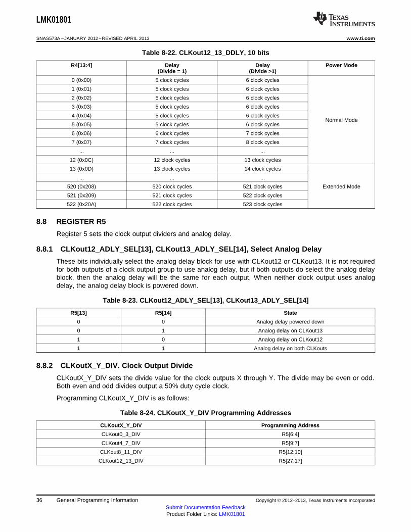
LMK01801
SNAS573A –JANUARY 2012–REVISED APRIL 2013 www.ti.com
Table 8-22. CLKout12_13_DDLY, 10 bits
R4[13:4] Delay Delay Power Mode(Divide = 1) (Divide >1)
0 (0x00) 5 clock cycles 6 clock cycles
1 (0x01) 5 clock cycles 6 clock cycles
2 (0x02) 5 clock cycles 6 clock cycles
3 (0x03) 5 clock cycles 6 clock cycles
4 (0x04) 5 clock cycles 6 clock cyclesNormal Mode
5 (0x05) 5 clock cycles 6 clock cycles
6 (0x06) 6 clock cycles 7 clock cycles
7 (0x07) 7 clock cycles 8 clock cycles
... ... ...
12 (0x0C) 12 clock cycles 13 clock cycles
13 (0x0D) 13 clock cycles 14 clock cycles
... ... ...
520 (0x208) 520 clock cycles 521 clock cycles Extended Mode
521 (0x209) 521 clock cycles 522 clock cycles
522 (0x20A) 522 clock cycles 523 clock cycles
8.8 REGISTER R5
Register 5 sets the clock output dividers and analog delay.
8.8.1 CLKout12_ADLY_SEL[13], CLKout13_ADLY_SEL[14], Select Analog Delay
These bits individually select the analog delay block for use with CLKout12 or CLKout13. It is not requiredfor both outputs of a clock output group to use analog delay, but if both outputs do select the analog delayblock, then the analog delay will be the same for each output. When neither clock output uses analogdelay, the analog delay block is powered down.
Table 8-23. CLKout12_ADLY_SEL[13], CLKout13_ADLY_SEL[14]
R5[13] R5[14] State
0 0 Analog delay powered down
0 1 Analog delay on CLKout13
1 0 Analog delay on CLKout12
1 1 Analog delay on both CLKouts
8.8.2 CLKoutX_Y_DIV. Clock Output Divide
CLKoutX_Y_DIV sets the divide value for the clock outputs X through Y. The divide may be even or odd.Both even and odd divides output a 50% duty cycle clock.
Programming CLKoutX_Y_DIV is as follows:
Table 8-24. CLKoutX_Y_DIV Programming Addresses
CLKoutX_Y_DIV Programming Address
CLKout0_3_DIV R5[6:4]
CLKout4_7_DIV R5[9:7]
CLKout8_11_DIV R5[12:10]
CLKout12_13_DIV R5[27:17]
36 General Programming Information Copyright © 2012–2013, Texas Instruments Incorporated
Submit Documentation FeedbackProduct Folder Links: LMK01801
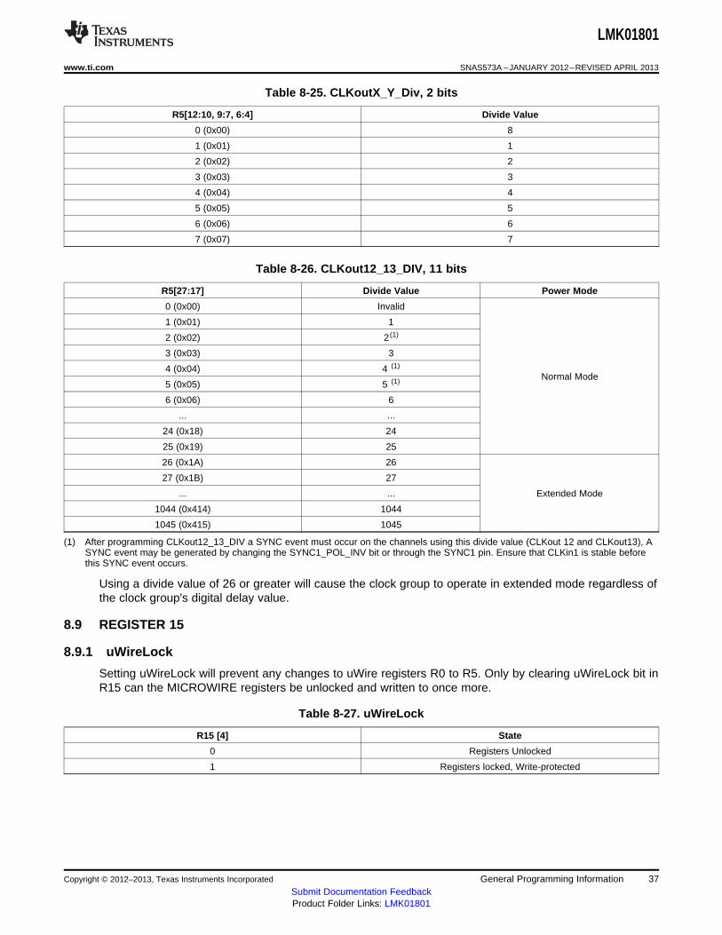
LMK01801
www.ti.com SNAS573A –JANUARY 2012–REVISED APRIL 2013
Table 8-25. CLKoutX_Y_Div, 2 bits
R5[12:10, 9:7, 6:4] Divide Value
0 (0x00) 8
1 (0x01) 1
2 (0x02) 2
3 (0x03) 3
4 (0x04) 4
5 (0x05) 5
6 (0x06) 6
7 (0x07) 7
Table 8-26. CLKout12_13_DIV, 11 bits
R5[27:17] Divide Value Power Mode
0 (0x00) Invalid
1 (0x01) 1
2 (0x02) 2 (1)
3 (0x03) 3
4 (0x04) 4 (1)
Normal Mode5 (0x05) 5 (1)
6 (0x06) 6
... ...
24 (0x18) 24
25 (0x19) 25
26 (0x1A) 26
27 (0x1B) 27
... ... Extended Mode
1044 (0x414) 1044
1045 (0x415) 1045
(1) After programming CLKout12_13_DIV a SYNC event must occur on the channels using this divide value (CLKout 12 and CLKout13), ASYNC event may be generated by changing the SYNC1_POL_INV bit or through the SYNC1 pin. Ensure that CLKin1 is stable beforethis SYNC event occurs.
Using a divide value of 26 or greater will cause the clock group to operate in extended mode regardless ofthe clock group's digital delay value.
8.9 REGISTER 15
8.9.1 uWireLock
Setting uWireLock will prevent any changes to uWire registers R0 to R5. Only by clearing uWireLock bit inR15 can the MICROWIRE registers be unlocked and written to once more.
Table 8-27. uWireLock
R15 [4] State
0 Registers Unlocked
1 Registers locked, Write-protected
Copyright © 2012–2013, Texas Instruments Incorporated General Programming Information 37Submit Documentation FeedbackProduct Folder Links: LMK01801

LMK01801
SNAS573A –JANUARY 2012–REVISED APRIL 2013 www.ti.com
9 Application Information
9.1 POWER SUPPLY
9.1.1 Current Consumption
NOTEAssuming θJA = 25.8 °C/W, the total power dissipated on chip must be less than (125 °C - 85°C) / 25.8 °C/W = 1.5 W to ensure a junction temperature less than 145 °C.
Worst case power dissipation can be estimated by multiplying typical power dissipation witha factor of 1.20.
From Table 9-1 the current consumption can be calculated for any configuration.
For example, the current for the entire device with 1 LVDS (CLKout0) and 1 LVPECL 1600 mVpp /w 240Ω emitter resistors (CLKout1) output active with a clock output divide = 1, and no other features enabledcan be calculated by adding the following blocks:• Core Current• Clock Buffer• One LVDS Output Buffer Current• Bank A• Output Divider Buffer Current• LVPECL 1600 mVpp buffer /w 240 Ω emitter resistors
Since there will be one LVPECL output drawing emitter current, this means some of the power from thecurrent draw of the device is dissipated in the external emitter resistors which doesn't add to the powerdissipation budget for the device but is important for LDO ICC calculations.
For total current consumption of the device add up the significant functional blocks. In this example 92 mA=• 1 mA (core current)• 22 mA (Bank A current)• 15 mA (Output Buffer current)• 21 mA (Output Divider current)• 9 mA (LVDS output current)• 24 mA (LVPECL 1600 mVpp buffer /w 240 Ω emitter resistors)
Once the total current consumption has been calculated, power dissipated by the device can becalculated. The power dissipation of the device is equel to the total current entering the device multipliedby the voltage at the device minus the power dissipated in any emitter resistors connected to any of theLVPECL outputs. If no emitter resistors are connected to the LVPECL outputs, this power will be 0 watts.Continuing the output with 240 Ω emitter resistors. Total IC power = 275.1 mW = 3.3 V * 95 mA -28.5 mW.
38 Application Information Copyright © 2012–2013, Texas Instruments Incorporated
Submit Documentation FeedbackProduct Folder Links: LMK01801

LMK01801
www.ti.com SNAS573A –JANUARY 2012–REVISED APRIL 2013
Table 9-1. Typical Current Consumption for Selected Functional Blocks(TA = 25 °C, VCC = 3.3 V)
PowerPower dissipatedTypical ICC dissipatedBlock Condition externally(mA) in device (mW)(mW) (1)
Core
Core All outputs and dividers off 1 3.3 -
Bank A At least on output enabled 22 72.6 -Bank
Bank B At least on output enabled 25 82.5 -
CLKout0 to CLKout3 -
CLKout4 to CLKout7 -On when any on output in the group isBuffers 15 49.5enabledCLKout8 to CLKout11 -
CLKout12 to CLKout13 -
Divide = 1 21 69.3 -CLKout0 to CLKout11
Divide = 2 to 8 24.2 79.8 -OutputDivider Divide = 1 to 25 and DDLY = 1 to 12 15 49.5 -
CLKout12 and CLKout13Divide = 26 to 1045 or DDLY > 13 19.1 63.0 -
Bank A Divide = 2 to 8 -Input 9 29.7Divider Bank B Divide = 2 to 8 -
CLKout12_13_ADLY = 0 to 3 3.4 11.2 -
CLKout12_13_ADLY = 4 to 7 3.8 12.5 -
Analog Delay Value CLKout12_13_ADLY = 8 to 11 4.2 13.9 -AnalogDelay CLKout12_13_ADLY = 12 to 15 4.7 15.5 -
CLKout12_13_ADLY = 16 to 23 5.2 17.2 -
When only one, CLKout12 or CLKout13, have Analog Delay Selected. 2.8 9.2 -
Clock Output Buffers
CLkout0 to CLKout11; 100 Ω differential termination 9 29.7 -LVDS
CLkout12 to CLKout13; 100 Ω differential termination 14 46.2 -
CLkout0 to CLKout11; LVPECL 1600mVpp, 24 79.2 28.5
AC coupled using 240 Ω emitter resistorsLVPECL CLkout12 to CLKout13; LVPECL 1600
mVpp, 29.5 97.3 28.5AC coupled using 240 Ω emitter resistors
10 MHz 18.6 61.4 -LVCMOS Pair, CLKout4 to CLKout11, 50 MHz 23.1 76.2 -(CLKoutX_TYPE = 6 - 10), CL = 5 pF
150 MHz 31.7 104.6 -
10 MHz 24.7 81.51 -LVCMOS Pair, CLKout12 and CLKout13, 50 MHz 30.3 100 -(CLKoutX_TYPE = 6 - 10), CL = 5 pF
150 MHz 42.0 138.6 -LVCMOS 10 MHz 9.7 32 -
LVCMOS Single, CLKout4 to CLKout11, 50 MHz 10.8 35.6 -(CLKoutX_TYPE=11 - 13), CL = 5 pF150 MHz 13.5 44.5 -
10 MHz 15 49.5 -LVCMOS Single, CLKout12 and CLKout13, 50 MHz 17.5 57.7 -(CLKoutX_TYPE= 11 - 13), CL = 5 pF
150 MHz 22.8 75.2 -
(1) Power is dissipated externally in LVPECL emitter resistors. The externally dissipated power is calculated as twice the DC voltage levelof one LVPECL clock output pin squared over the emitter resistance. That is to say power dissipated in emitter resistors = 2 * Vem
2/Rem
Copyright © 2012–2013, Texas Instruments Incorporated Application Information 39Submit Documentation FeedbackProduct Folder Links: LMK01801

LMK01801
SNAS573A –JANUARY 2012–REVISED APRIL 2013 www.ti.com
9.2 PIN CONNECTION RECOMMENDATIONS
9.2.1 Vcc Pins and Decoupling
All Vcc pins must always be connected.
Integrated capacitance on the IC makes high frequency decoupling capacitors unnecessary. Ferrite beadsshould be used on CLKout Vcc pins to minimize crosstalk through power supply. When several clocksshare the same frequency, a single ferrite bead can be shared with the common frequency CLKout Vcc'sfor power supply isolation.
9.2.2 Unused clock outputs
Leave unused clock outputs floating and powered down.
9.2.3 Unused clock inputs
Unused clock inputs can be left floating.
9.2.4 Bias
Proper bypassing of the Bias pin with a 1 µF capacitor connected to Vcc4_Bias (Pin 25) is important forlow noise performance.
9.2.5 In MICROWIRE Mode
SYNC0 and SYNC1 have an internal pullup and may be left as a no-connect if external SYNC is notrequired. MIRCROWIRE SYNC may still be used in this condition.
9.3 THERMAL MANAGEMENT
Power consumption of the LMK01801 can be high enough to require attention to thermal management.For reliability and performance reasons the die temperature should be limited to a maximum of 125 °C.That is, as an estimate, TA (ambient temperature) plus device power consumption times θJA should notexceed 125 °C.
The package of the device has an exposed pad that provides the primary heat removal path as well asexcellent electrical grounding to a printed circuit board. To maximize the removal of heat from the packagea thermal land pattern including multiple vias to a ground plane must be incorporated on the PCB withinthe footprint of the package. The exposed pad must be soldered down to ensure adequate heatconduction out of the package.
A recommended footprint including recommended solder mask and solder paste layers can be found at:http://www.ti.com/packaging for the RHS0048A package.
40 Application Information Copyright © 2012–2013, Texas Instruments Incorporated
Submit Documentation FeedbackProduct Folder Links: LMK01801

0.1 PF
0.1 PFLMK01801Input10
0:100:Trace(Differential)
Differential Sinewave Clock
Source
CLKinX
CLKinX*
0.1 PF
0.1 PFLMK01801Input10
0:100:Trace(Differential)
CLKinX
CLKinX*
LVPECLRef Clk
240:
240:
0.1 PF
0.1 PF
0.1 PF
0.1 PFLMK01801
Input100:100:Trace
(Differential)
CLKinX
CLKinX*
LVDS
LMK01801
www.ti.com SNAS573A –JANUARY 2012–REVISED APRIL 2013
9.4 DRIVING CLKin INPUTS
9.4.1 Driving CLKin Pins with a Differential Source
Both CLKin ports can be driven by differential signals. It is recommended that the input mode be set tobipolar (CLKinX_BUF_TYPE = 0) when using differential reference clocks. The LMK01801 family internallybiases the input pins so the differential interface should be AC coupled. The recommended circuits fordriving the CLKin pins with either LVDS or LVPECL are shown in Figure 9-1 and Figure 9-2.
Figure 9-1. CLKinX/X* Termination for an LVDSReference Clock Source
Figure 9-2. CLKinX/X* Termination for an LVPECLReference Clock Source
Finally, a reference clock source that produces a differential sine wave output can drive the CLKin pinsusing the circuit shown in Figure 9-3. Note: the signal level must conform to the requirements for theCLKin pins listed in the Section 3.4.
Figure 9-3. CLKinX/X* Single-ended Termination
9.4.2 Driving CLKin Pins with a Single-Ended Source
The CLKin pins of the LMK01801 family can be driven using a single-ended reference clock source, forexample, either a sine wave source or an LVCMOS/LVTTL source. Either AC coupling or DC couplingmay be used. In the case of the sine wave source that is expecting a 50 Ω load, it is recommended thatAC coupling be used as shown in Figure 9-4 the circuit below with a 50 Ω termination.
NOTEThe signal level must conform to the requirements for the CLKin pins listed in theSection 3.4. CLKinX_BUF_TYPE is recommended to be set to bipolar mode(CLKinX_BUF_TYPE = 0).
Copyright © 2012–2013, Texas Instruments Incorporated Application Information 41Submit Documentation FeedbackProduct Folder Links: LMK01801

0.1 PF
0.1 PF
50:Trace
50: LMK01801Clock Source
CLKinX
CLKinX*
LMK01801
SNAS573A –JANUARY 2012–REVISED APRIL 2013 www.ti.com
Figure 9-4. DC Coupled LVCMOS/LVTTLReference Clock
If the CLKin pins are being driven with a single-ended LVCMOS/ LVTTL source, either DC coupling or ACcoupling may be used. If DC coupling is used, see Figure 9-5, the CLKinX_BUF_TYPE should be set toMOS buffer mode (CLKinX_BUF_TYPE = 1) and the voltage swing of the source must meet thespecifications for DC coupled, MOS-mode clock inputs given in the table of Electrical Characteristics. IfAC coupling is used, the CLKinX_BUF_TYPE should be set to the bipolar buffer mode(CLKinX_BUF_TYPE = 0). The voltage swing at the input pins must meet the specifications for ACcoupled, bipolar mode clock inputs given in the table of Electrical Characteristics. In this case, someattenuation of the clock input level may be required. A simple resistive divider circuit before the ACcoupling capacitor is sufficient.
Figure 9-5. DC Coupled LVCMOS/LVTTL ReferenceClock
9.5 TERMINATION AND USE OF CLOCK OUTPUT (DRIVERS)
When terminating clock drivers keep in mind these guidelines for optimum phase noise and jitterperformance:• Transmission line theory should be followed for good impedance matching to prevent reflections.• Clock drivers should be presented with the proper loads. For example:
– LVDS drivers are current drivers and require a closed current loop.– LVPECL drivers are open emitters and require a DC path to ground.
• Receivers should be presented with a signal biased to their specified DC bias level (common modevoltage) for proper operation. Some receivers have self-biasing inputs that automatically bias to theproper voltage level. In this case, the signal should normally be AC coupled.
It is possible to drive a non-LVPECL or non-LVDS receiver with an LVDS or LVPECL driver as long as theabove guidelines are followed. Check the datasheet of the receiver or input being driven to determine thebest termination and coupling method to be sure that the receiver is biased at its optimum DC voltage(common mode voltage).
For example, when driving the OSCin/OSCin* input of the LMK04800 family, OSCin/OSCin* should be ACcoupled because OSCin/ OSCin* biases the signal to the proper DC level. This is only slightly differentfrom the AC coupled cases described in Section 9.4.2 because the DC blocking capacitors are placedbetween the termination and the OSCin/OSCin* pins, but the concept remains the same. The receiver(OSCin/OSCin*) sets the input to the optimum DC bias voltage (common mode voltage), not the driver.
42 Application Information Copyright © 2012–2013, Texas Instruments Incorporated
Submit Documentation FeedbackProduct Folder Links: LMK01801

CLKoutX
CLKoutX*
LVPECL Receiver
120:
100:Trace(Differential)
120:
Vcc
Vcc
LVPECL Driver
82:
82:
CLKoutX
CLKoutX*
LVPECL Receiver
50:
100:Trace(Differential)
50:
Vcc - 2 V
Vcc - 2 V
LVPECL Driver
CLKoutX
CLKoutX*
LVDS Receiver10
0:100:Trace(Differential)
LVDSDriver
LMK01801
www.ti.com SNAS573A –JANUARY 2012–REVISED APRIL 2013
9.5.1 Termination for DC Coupled Differential Operation
For DC coupled operation of an LVDS driver, terminate with 100 Ω as close as possible to the LVDSreceiver as shown in Figure 9-6.
Figure 9-6. Differential LVDS Operation, DC Coupling, No Biasing of the Receiver
For DC coupled operation of an LVPECL driver, terminate with 50 Ω to VCC - 2 V as shown in Figure 9-7.Alternatively terminate with a Thevenin equivalent circuit (120 Ω resistor connected to VCC and an 82 Ωresistor connected to ground with the driver connected to the junction of the 120 Ω and 82 Ω resistors) asshown in Figure 9-8 for VCC = 3.3 V.
Figure 9-7. Differential LVPECL Operation, DC Coupling
Figure 9-8. Differential LVPECL Operation, DC Coupling, Thevenin Equivalent
9.5.2 Termination for AC Coupled Differential Operation
AC coupling allows for shifting the DC bias level (common mode voltage) when driving different receiverstandards. Since AC coupling prevents the driver from providing a DC bias voltage at the receiver it isimportant to ensure the receiver is biased to its ideal DC level.
When driving non-biased LVDS receivers with an LVDS driver, the signal may be AC coupled by addingDC blocking capacitors, however the proper DC bias point needs to be established at the receiver. Oneway to do this is with the termination circuitry in Figure 9-9.
Copyright © 2012–2013, Texas Instruments Incorporated Application Information 43Submit Documentation FeedbackProduct Folder Links: LMK01801

CLKoutX
CLKoutX*
Rem
Rem
0.1 PF
0.1 PF
DifferentialInput
100:Trace(Differential)
LVPECLDriver 10
0:
CA
CA
0.1 PF
0.1 PF
LVDSReceiver
100:Trace(Differential)
LVDSDriver 10
0:
CLKoutX
CLKoutX*
0.1 PF
0.1 PF
LVDS Receiver
50:
100:Trace(Differential)
LVDSDriver
50:
Vbias
LMK01801
SNAS573A –JANUARY 2012–REVISED APRIL 2013 www.ti.com
Figure 9-9. Differential LVDS Operation, AC Coupling, External Biasing at the Receiver
Some LVDS receivers may have internal biasing on the inputs. In this case, the circuit shown in ismodified by replacing the 50 Ω terminations to Vbias with a single 100 Ω resistor across the input pins ofthe receiver, as shown in Figure 9-10. When using AC coupling with LVDS outputs, there may be astartup delay observed in the clock output due to capacitor charging. The previous figures employ a 0.1μF capacitor. This value may need to be adjusted to meet the startup requirements for a particularapplication.
Figure 9-10. LVDS Termination for a Self-Biased Receiver
LVPECL drivers require a DC path to ground. When AC coupling an LVPECL signal use 120 Ω to 240 Ωemitter resistors close to the LVPECL driver to provide a DC path to ground as shown in Figure 9-11. Forproper receiver operation, the signal should be biased to the DC bias level (common mode voltage)specified by the receiver. The typical DC bias voltage for LVPECL receivers is 2 V.
A typical application is shown in Figure 9-11, where Rem=120 Ω to 240 Ω. Refer to the reciever inputrecommendations to determine if the proper value of CA's, if needed.
Figure 9-11. Differential LVPECL Operation, AC Coupling,External Biasing at the Receiver,
Rem=120 Ω to 240 Ω
9.5.3 Termination for Single-Ended Operation
A balun can be used with either LVDS or LVPECL drivers to convert the balanced, differential signal intoan unbalanced, single-ended signal.
44 Application Information Copyright © 2012–2013, Texas Instruments Incorporated
Submit Documentation FeedbackProduct Folder Links: LMK01801

CLKoutX
CLKoutX*
120:
120:
0.1 PF
0.1 PF
50:Trace
50:
Load50:
LVPECLDriver
CLKoutX
CLKoutX*
50:Trace
120:
Load
Vcc
82:
120:
VccLVPECL
Driver
82:
CLKoutX
CLKoutX* 50:
50:Trace
50:
Load
Vcc - 2V
Vcc - 2VLVPECL
Driver
LMK01801
www.ti.com SNAS573A –JANUARY 2012–REVISED APRIL 2013
It is possible to use an LVPECL driver as one or two separate 800 mVpp signals. When using only oneLVPECL driver of a CLKoutX/CLKoutX* pair, be sure to properly terminated the unused driver. When DCcoupling one of the LMK04800 family clock LVPECL drivers, the termination should be 50 Ω to VCC - 2 Vas shown in Figure 9-12. The Thevenin equivalent circuit is also a valid termination as shown in Figure 9-13 for Vcc = 3.3 V.
Figure 9-12. Single-Ended LVPECL Operation,DC Coupling
Figure 9-13. Single-Ended LVPECL Operation, DCCoupling, Thevenin Equivalent
When AC coupling an LVPECL driver use a 120 Ω to 240 Ω emitter resistor to provide a DC path toground and ensure a 50 Ω termination with the proper DC bias level for the receiver. The typical DC biasvoltage for LVPECL receivers is 2 V (See Section 9.5.2). If the companion driver is not used it should beterminated with either a proper AC or DC termination. This latter example of AC coupling a single-endedLVPECL signal can be used to measure single-ended LVPECL performance using a spectrum analyzer orphase noise analyzer. When using most RF test equipment no DC bias point (0 VDC) is required for safeand proper operation. The internal 50 Ω termination of the test equipment correctly terminates theLVPECL driver being measured as shown in Figure 9-14.
Figure 9-14. Single-Ended LVPECL Operation, AC CouplingRem=120 Ω to 240 Ω
Copyright © 2012–2013, Texas Instruments Incorporated Application Information 45Submit Documentation FeedbackProduct Folder Links: LMK01801

LMK01801
SNAS573A –JANUARY 2012–REVISED APRIL 2013 www.ti.com
Revision HistoryNOTE: Page numbers for previous revisions may differ from page numbers in the current version.
Changes from Original (April 2013) to Revision A Page
• Changed layout of National Data Sheet to TI format .......................................................................... 45
46 Application Information Copyright © 2012–2013, Texas Instruments Incorporated
Submit Documentation FeedbackProduct Folder Links: LMK01801
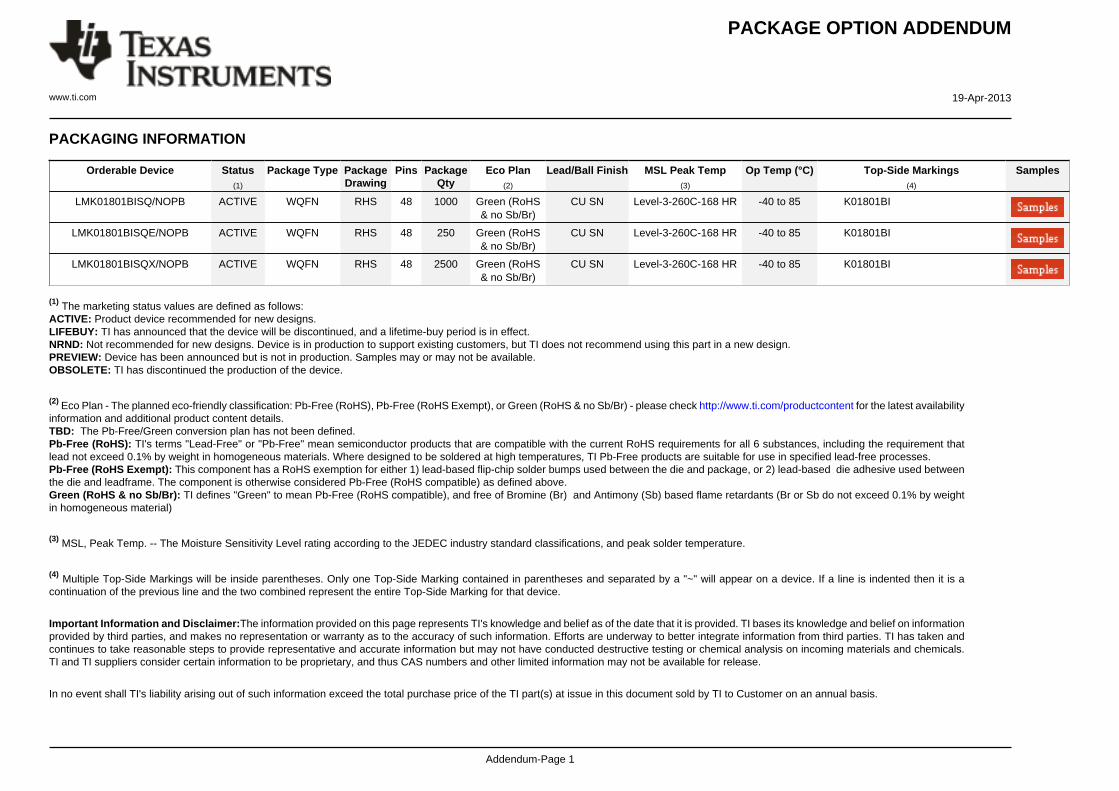
PACKAGE OPTION ADDENDUM
www.ti.com 19-Apr-2013
Addendum-Page 1
PACKAGING INFORMATION
Orderable Device Status(1)
Package Type PackageDrawing
Pins PackageQty
Eco Plan(2)
Lead/Ball Finish MSL Peak Temp(3)
Op Temp (°C) Top-Side Markings(4)
Samples
LMK01801BISQ/NOPB ACTIVE WQFN RHS 48 1000 Green (RoHS& no Sb/Br)
CU SN Level-3-260C-168 HR -40 to 85 K01801BI
LMK01801BISQE/NOPB ACTIVE WQFN RHS 48 250 Green (RoHS& no Sb/Br)
CU SN Level-3-260C-168 HR -40 to 85 K01801BI
LMK01801BISQX/NOPB ACTIVE WQFN RHS 48 2500 Green (RoHS& no Sb/Br)
CU SN Level-3-260C-168 HR -40 to 85 K01801BI
(1) The marketing status values are defined as follows:ACTIVE: Product device recommended for new designs.LIFEBUY: TI has announced that the device will be discontinued, and a lifetime-buy period is in effect.NRND: Not recommended for new designs. Device is in production to support existing customers, but TI does not recommend using this part in a new design.PREVIEW: Device has been announced but is not in production. Samples may or may not be available.OBSOLETE: TI has discontinued the production of the device.
(2) Eco Plan - The planned eco-friendly classification: Pb-Free (RoHS), Pb-Free (RoHS Exempt), or Green (RoHS & no Sb/Br) - please check http://www.ti.com/productcontent for the latest availabilityinformation and additional product content details.TBD: The Pb-Free/Green conversion plan has not been defined.Pb-Free (RoHS): TI's terms "Lead-Free" or "Pb-Free" mean semiconductor products that are compatible with the current RoHS requirements for all 6 substances, including the requirement thatlead not exceed 0.1% by weight in homogeneous materials. Where designed to be soldered at high temperatures, TI Pb-Free products are suitable for use in specified lead-free processes.Pb-Free (RoHS Exempt): This component has a RoHS exemption for either 1) lead-based flip-chip solder bumps used between the die and package, or 2) lead-based die adhesive used betweenthe die and leadframe. The component is otherwise considered Pb-Free (RoHS compatible) as defined above.Green (RoHS & no Sb/Br): TI defines "Green" to mean Pb-Free (RoHS compatible), and free of Bromine (Br) and Antimony (Sb) based flame retardants (Br or Sb do not exceed 0.1% by weightin homogeneous material)
(3) MSL, Peak Temp. -- The Moisture Sensitivity Level rating according to the JEDEC industry standard classifications, and peak solder temperature.
(4) Multiple Top-Side Markings will be inside parentheses. Only one Top-Side Marking contained in parentheses and separated by a "~" will appear on a device. If a line is indented then it is acontinuation of the previous line and the two combined represent the entire Top-Side Marking for that device.
Important Information and Disclaimer:The information provided on this page represents TI's knowledge and belief as of the date that it is provided. TI bases its knowledge and belief on informationprovided by third parties, and makes no representation or warranty as to the accuracy of such information. Efforts are underway to better integrate information from third parties. TI has taken andcontinues to take reasonable steps to provide representative and accurate information but may not have conducted destructive testing or chemical analysis on incoming materials and chemicals.TI and TI suppliers consider certain information to be proprietary, and thus CAS numbers and other limited information may not be available for release.
In no event shall TI's liability arising out of such information exceed the total purchase price of the TI part(s) at issue in this document sold by TI to Customer on an annual basis.

TAPE AND REEL INFORMATION
*All dimensions are nominal
Device PackageType
PackageDrawing
Pins SPQ ReelDiameter
(mm)
ReelWidth
W1 (mm)
A0(mm)
B0(mm)
K0(mm)
P1(mm)
W(mm)
Pin1Quadrant
LMK01801BISQ/NOPB WQFN RHS 48 1000 330.0 16.4 7.3 7.3 1.3 12.0 16.0 Q1
LMK01801BISQE/NOPB WQFN RHS 48 250 178.0 16.4 7.3 7.3 1.3 12.0 16.0 Q1
LMK01801BISQX/NOPB WQFN RHS 48 2500 330.0 16.4 7.3 7.3 1.3 12.0 16.0 Q1
PACKAGE MATERIALS INFORMATION
www.ti.com 20-Sep-2016
Pack Materials-Page 1
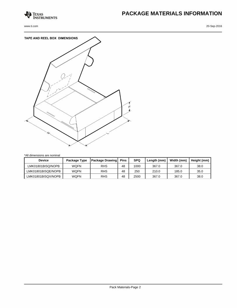
*All dimensions are nominal
Device Package Type Package Drawing Pins SPQ Length (mm) Width (mm) Height (mm)
LMK01801BISQ/NOPB WQFN RHS 48 1000 367.0 367.0 38.0
LMK01801BISQE/NOPB WQFN RHS 48 250 210.0 185.0 35.0
LMK01801BISQX/NOPB WQFN RHS 48 2500 367.0 367.0 38.0
PACKAGE MATERIALS INFORMATION
www.ti.com 20-Sep-2016
Pack Materials-Page 2

IMPORTANT NOTICE
Texas Instruments Incorporated (TI) reserves the right to make corrections, enhancements, improvements and other changes to itssemiconductor products and services per JESD46, latest issue, and to discontinue any product or service per JESD48, latest issue. Buyersshould obtain the latest relevant information before placing orders and should verify that such information is current and complete.TI’s published terms of sale for semiconductor products (http://www.ti.com/sc/docs/stdterms.htm) apply to the sale of packaged integratedcircuit products that TI has qualified and released to market. Additional terms may apply to the use or sale of other types of TI products andservices.Reproduction of significant portions of TI information in TI data sheets is permissible only if reproduction is without alteration and isaccompanied by all associated warranties, conditions, limitations, and notices. TI is not responsible or liable for such reproduceddocumentation. Information of third parties may be subject to additional restrictions. Resale of TI products or services with statementsdifferent from or beyond the parameters stated by TI for that product or service voids all express and any implied warranties for theassociated TI product or service and is an unfair and deceptive business practice. TI is not responsible or liable for any such statements.Buyers and others who are developing systems that incorporate TI products (collectively, “Designers”) understand and agree that Designersremain responsible for using their independent analysis, evaluation and judgment in designing their applications and that Designers havefull and exclusive responsibility to assure the safety of Designers' applications and compliance of their applications (and of all TI productsused in or for Designers’ applications) with all applicable regulations, laws and other applicable requirements. Designer represents that, withrespect to their applications, Designer has all the necessary expertise to create and implement safeguards that (1) anticipate dangerousconsequences of failures, (2) monitor failures and their consequences, and (3) lessen the likelihood of failures that might cause harm andtake appropriate actions. Designer agrees that prior to using or distributing any applications that include TI products, Designer willthoroughly test such applications and the functionality of such TI products as used in such applications.TI’s provision of technical, application or other design advice, quality characterization, reliability data or other services or information,including, but not limited to, reference designs and materials relating to evaluation modules, (collectively, “TI Resources”) are intended toassist designers who are developing applications that incorporate TI products; by downloading, accessing or using TI Resources in anyway, Designer (individually or, if Designer is acting on behalf of a company, Designer’s company) agrees to use any particular TI Resourcesolely for this purpose and subject to the terms of this Notice.TI’s provision of TI Resources does not expand or otherwise alter TI’s applicable published warranties or warranty disclaimers for TIproducts, and no additional obligations or liabilities arise from TI providing such TI Resources. TI reserves the right to make corrections,enhancements, improvements and other changes to its TI Resources. TI has not conducted any testing other than that specificallydescribed in the published documentation for a particular TI Resource.Designer is authorized to use, copy and modify any individual TI Resource only in connection with the development of applications thatinclude the TI product(s) identified in such TI Resource. NO OTHER LICENSE, EXPRESS OR IMPLIED, BY ESTOPPEL OR OTHERWISETO ANY OTHER TI INTELLECTUAL PROPERTY RIGHT, AND NO LICENSE TO ANY TECHNOLOGY OR INTELLECTUAL PROPERTYRIGHT OF TI OR ANY THIRD PARTY IS GRANTED HEREIN, including but not limited to any patent right, copyright, mask work right, orother intellectual property right relating to any combination, machine, or process in which TI products or services are used. Informationregarding or referencing third-party products or services does not constitute a license to use such products or services, or a warranty orendorsement thereof. Use of TI Resources may require a license from a third party under the patents or other intellectual property of thethird party, or a license from TI under the patents or other intellectual property of TI.TI RESOURCES ARE PROVIDED “AS IS” AND WITH ALL FAULTS. TI DISCLAIMS ALL OTHER WARRANTIES ORREPRESENTATIONS, EXPRESS OR IMPLIED, REGARDING RESOURCES OR USE THEREOF, INCLUDING BUT NOT LIMITED TOACCURACY OR COMPLETENESS, TITLE, ANY EPIDEMIC FAILURE WARRANTY AND ANY IMPLIED WARRANTIES OFMERCHANTABILITY, FITNESS FOR A PARTICULAR PURPOSE, AND NON-INFRINGEMENT OF ANY THIRD PARTY INTELLECTUALPROPERTY RIGHTS. TI SHALL NOT BE LIABLE FOR AND SHALL NOT DEFEND OR INDEMNIFY DESIGNER AGAINST ANY CLAIM,INCLUDING BUT NOT LIMITED TO ANY INFRINGEMENT CLAIM THAT RELATES TO OR IS BASED ON ANY COMBINATION OFPRODUCTS EVEN IF DESCRIBED IN TI RESOURCES OR OTHERWISE. IN NO EVENT SHALL TI BE LIABLE FOR ANY ACTUAL,DIRECT, SPECIAL, COLLATERAL, INDIRECT, PUNITIVE, INCIDENTAL, CONSEQUENTIAL OR EXEMPLARY DAMAGES INCONNECTION WITH OR ARISING OUT OF TI RESOURCES OR USE THEREOF, AND REGARDLESS OF WHETHER TI HAS BEENADVISED OF THE POSSIBILITY OF SUCH DAMAGES.Unless TI has explicitly designated an individual product as meeting the requirements of a particular industry standard (e.g., ISO/TS 16949and ISO 26262), TI is not responsible for any failure to meet such industry standard requirements.Where TI specifically promotes products as facilitating functional safety or as compliant with industry functional safety standards, suchproducts are intended to help enable customers to design and create their own applications that meet applicable functional safety standardsand requirements. Using products in an application does not by itself establish any safety features in the application. Designers mustensure compliance with safety-related requirements and standards applicable to their applications. Designer may not use any TI products inlife-critical medical equipment unless authorized officers of the parties have executed a special contract specifically governing such use.Life-critical medical equipment is medical equipment where failure of such equipment would cause serious bodily injury or death (e.g., lifesupport, pacemakers, defibrillators, heart pumps, neurostimulators, and implantables). Such equipment includes, without limitation, allmedical devices identified by the U.S. Food and Drug Administration as Class III devices and equivalent classifications outside the U.S.TI may expressly designate certain products as completing a particular qualification (e.g., Q100, Military Grade, or Enhanced Product).Designers agree that it has the necessary expertise to select the product with the appropriate qualification designation for their applicationsand that proper product selection is at Designers’ own risk. Designers are solely responsible for compliance with all legal and regulatoryrequirements in connection with such selection.Designer will fully indemnify TI and its representatives against any damages, costs, losses, and/or liabilities arising out of Designer’s non-compliance with the terms and provisions of this Notice.
Mailing Address: Texas Instruments, Post Office Box 655303, Dallas, Texas 75265Copyright © 2017, Texas Instruments Incorporated