Embed Size (px)
Citation preview
V2S-R7 FPGA Engineering Specification
Copyright © 2012 ARM Limited. All rights reserved. Page 1 of 20
V2S-R7 FPGA Engineering Specification
System Design Division
Document number: V2S-R7 EIS
Date of Issue: August 23, 2012
Authors: SDPL
© Copyright ARM Limited 2010-2012. All rights reserved.
Abstract
This document describes a Cortex-R7 Soft Macrocell Model implemented using LogicTile Express 13MG V2F-2XV6 board.
Keywords
Cortex, R7, FPGA, SMM, CoreSight, Versatile Express Platform.
V2S-R7 FPGA Engineering Specification
Copyright © 2012 ARM Limited. All rights reserved. Page 2 of 20
Contents
1 ABOUT THIS DOCUMENT 3 1.1 Change control 3
1.1.1 Current status and anticipated changes 3 1.1.2 Change history 3
1.2 References 3 1.3 Terms and abbreviations 4
2 SCOPE 5
3 INTRODUCTION 5
4 GETTING STARTED 6
5 OVERVIEW 7 5.1 General overview 7
5.1.1 Processor configurations 7 5.1.2 System level features 7
5.2 Debug features 7 5.2.1 CoreSight Sub-System 8 5.2.2 Debugger Access 9
5.3 FPGA Hardware 9 5.4 System Level Design 10
5.4.1 PL341 Dynamic Memory Controller 12 5.4.2 SCC controller 12 5.4.3 PL354 Static Memory Controller 12 5.4.4 ACP port 12 5.4.5 DMA controller 12 5.4.6 ZBT RAM controller 12 5.4.7 HCLCD controller 13 5.4.8 L2C-310 Level 2 Cache 13 5.4.9 CoreSight 13 5.4.10 Cortex-R7 13
5.5 Clock architecture 14 5.5.1 Default, minimum and maximum operating frequencies 14
6 MEMORY MAP 15 6.1 SCC/APB Register block 18
7 INTERRUPTS AND EVENTS SIGNALS 20 7.1 Interrupts 20
V2S-R7 FPGA Engineering Specification
Copyright © 2012 ARM Limited. All rights reserved. Page 3 of 20
1 ABOUT THIS DOCUMENT
1.1 Change control
1.1.1 Current status and anticipated changes
1.1.2 Change history
Brief descriptions of major changes are also described here:
Status Remark
1.0 First Release
1.2 References
This document refers to the following other documents:
Ref Doc No Author(s) Title
[1] ARM DUI 0447F ARM Ltd. Motherboard Express μATX (V2M-P1)
TRM
[2] ARM DDI 0424A ARM Ltd. PrimeCell DMA Controller (PL330)
Revision:r0p0 TRM
[3] ARM DDI 0397F ARM Ltd. AMBA Network Interconnect (NIC-301)
Revision:r2p0 TRM
[4] ARM DDI 0246F ARM Ltd. Level 2 Cache Controller (L2C-310)
Revision: r3p2 TRM
[5] ARM DDI 0418C ARM Ltd. DDR2 Dynamic Memory Controller (PL341) Revision: r0p1 TRM
V2S-R7 FPGA Engineering Specification
Copyright © 2012 ARM Limited. All rights reserved. Page 4 of 20
1.3 Terms and abbreviations
This document uses the following terms and abbreviations.
Term Meaning
AMBA Advanced Microcontroller Bus Architecture
ACP AXI Coherence Port
APB Advanced Peripheral Bus
ATB Advanced Trace Bus
AXI Advanced eXtensible Interface
SCC System Configuration Controller
DAP Debug Access Port
DMAC Direct Memory Access Control
ECC Error Correction Code
ETB Embedded Trace Buffer
FPU Floating-Point Unit
MPU Memory Protection Unit
PIL Processor Integration Layer
ETM
ETR
ETF
Embedded Trace Macro-cell
Embedded Trace Router
Embedded Trace FIFO
HPM High Performance Matrix
LLPP Low Latency Peripheral Port
SCU Snoop Control Unit
SVN SubVersioN, a version control system
TCM Tightly Coupled Memory
TPIU Trace Port Interface Unit
VIC Vectored Interrupt Controller
V2 Versatile Express
SMM Soft Macrocell Model
SMC Static Memory Controller
DMC Dynamic Memory Controller
DMA Direct Memory Access
DCC Daughterboard Configuration Controller
MMCM Mixed-Mode Clock Manager
V2S-R7 FPGA Engineering Specification
Copyright © 2012 ARM Limited. All rights reserved. Page 5 of 20
2 SCOPE
This document describes features that are unique to the Cortex-R7 Soft Macrocell Model (SMM) implemented on a LogicTile Express 13MG (V2F-2XV6). It will examine the contents of the SMM-R7, system interconnect, the
clock structure, and specifics of the programmer’s model directly relevant to SMM-R7 operation.
3 INTRODUCTION
In this configuration of the Cortex-R7 FPGA the Cortex-R7 CPU is implemented in an MP2 Split-Lock configuration. Processor nCPUHALT, SAFEMODE & COMPENABLE CPU features are controlled by the SCC peripheral in the 760 FPGA details of which can be found in section 6.1.
This FPGA image is a Cortex-R7 derivative processor that implements (in addition to existing CR7 features) the following:
Internal matrix synchronous to core clock.
CoreSight sub-system with JTAG, Serial Wire and Trace support internally and on board.
Asynchronous bridges to DDR memory and SMC interface.
Up to 2GB of DDR2 using SODIMM module,
SMC for Versatile Express motherboard accesses, additional peripherals (DMC, video/CLCD, DMA) included.
16MB of on board ZBTRAM synchronous to core.
Internal HDCLCD controller.
V2S-R7 FPGA Engineering Specification
Copyright © 2012 ARM Limited. All rights reserved. Page 6 of 20
4 GETTING STARTED
1. The SMM R7 operates on an ARM LogicTile Express 13MG (V2F-2XV6) daughterboard mounted on a Versatile Express motherboard (V2M-P1).
2. Ensure the LogicTile Express 13MG daughterboard is plugged into Site 2 of the Versatile Express Motherboard as described in Quick Start Guide for the Versatile Express Family - Adding Daughterboards.
3. Install the SMM R7 FPGA images and support files from the V2S-R7 installation CD onto a host computer running Microsoft Windows.
4. Connect USB, UART0, and power to the Versatile Express motherboard, and power up as described in Quick Start Guide for the Versatile Express Family - Powering up the System.
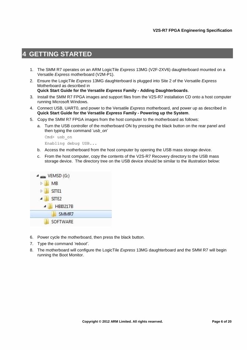
5. Copy the SMM R7 FPGA images from the host computer to the motherboard as follows:
a. Turn the USB controller of the motherboard ON by pressing the black button on the rear panel and then typing the command ‘usb_on’
Cmd> usb_on
Enabling debug USB...
b. Access the motherboard from the host computer by opening the USB mass storage device.
c. From the host computer, copy the contents of the V2S-R7 Recovery directory to the USB mass storage device. The directory tree on the USB device should be similar to the illustration below:
6. Power cycle the motherboard, then press the black button.
7. Type the command ‘reboot’.
8. The motherboard will configure the LogicTile Express 13MG daughterboard and the SMM R7 will begin
running the Boot Monitor.
V2S-R7 FPGA Engineering Specification
Copyright © 2012 ARM Limited. All rights reserved. Page 7 of 20
5 OVERVIEW
5.1 General overview
The SMM is based on R7 r0p0. The R7 Integration Level is used with additional logic wrapped around it.
5.1.1 Processor configuration
Processor feature Configuration Notes
I-cache CPU 0 : 16KB
CPU 1 : 16KB
-
D-cache CPU 0 : 16KB
CPU 1 : 16KB
-
MPU 12 or 16 regions (synthesis option)
-
TCM CPU 0 : 64KB x 2
CPU 1 : 64KB x 2
-
FPU CPU 0 : Yes
CPU 1 : Yes
-
SCU Present -
Table 5.1 Processor Configuration
5.1.2 System level features
System feature Configuration Notes
Level 2 cache Present - Connected to AXI master port and to AXI Bus Matrix (NIC301) slave port
AXI slave ports Present to AXI Bus Matrix (NIC301) and to CoreSight
AXI LLPP Present to AXI Bus Matrix (NIC301)
AHB LLPP Not supported Tied off
GIC Not Included
DMA Included to AXI Bus Matrix (NIC301)
Table 5.2 System level features
5.2 Debug features
Debug feature Configuration Notes
ETM 2 Present One for each processor. Located in the PIL
CoreSight Hugo Present Include CSTPIU, TMC-ETF. TMC-ETR, STM, CTI, DAP-AXIAP, DAP-APBAP & DAP-SWIDP
ROM table Two Primary ROM table for CSSYS
Secondary ROM table for for PIL
Table 5.3 Debug features
V2S-R7 FPGA Engineering Specification
Copyright © 2012 ARM Limited. All rights reserved. Page 8 of 20
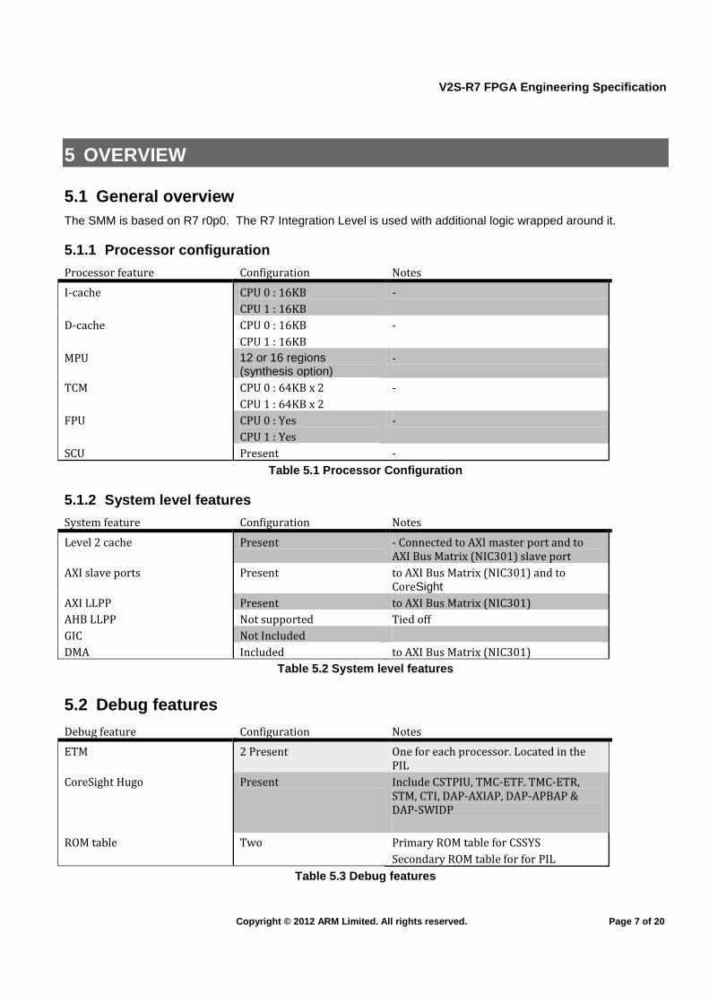
5.2.1 CoreSight Sub-System
The debug sub-system is a configuration of the Hugo CoreSight system. It features dual ATB interfaces, DAP SWI DP, TPIU (32-bit port width) for trace and TMC-ETR for trace data buffering.
TMC ETR
AT
B F
UN
NE
L
DOWNSIZER
UPSIZER
UPSIZER
ATB64
ATB64
ATBD0
ATBI0
ATBI1
ATBD1
ATB32
ATB32
ATB64
ATB64
APBIC
APB
APB
APB
APB
SYSAPB
AXI
s
AXI AXI
DAP
AXI AP
m
TPIU
s
ATB
m
s
ATB
DAP APB AP
DAP SWI DP
DAP BUS IC
m APB
DAP
APB
AXI
AXI
CTIs
APB
ATB64
APB
UPSIZERATB32STM
s
s
m
AXI
APB
Trace Port
SWJTAG
TMC ETF
s
ATB REPLICATOR
s
m
m
m
m
m
m
mCOREAPB
m
s
CSSYS
TSGENs
m
APB
TSENC63:0NTS
Replicator3:0
NTS
SyncBridge
NTS
SyncBridge
TSDEC
TSDEC
CPU TimeStamp
Figure 1 CoreSight Sub-System
Table 1 details the connectivity between the CTI TRIGOUT / TRIGIN ports and the rest of the CoreSight system components.
CTI TRIGOUT CTI TRIGIN
0 TMC-ETR Flush 0 TMC-ETF FULL
1 TMC-ETR TRIGIN 1 TMC-ETF ACQCOMP
2 TPIU Flush 2 TMC-ETR FULL
3 TPIU TRIGIN 3 TMC-ETR ACQCOMP
4 STM HWE [0, 1] 0 inverted 4 STM TRIGOUT SPTE
5 STM HWE [2, 3] 2 inverted 5 STM TRIGOUT SW
6 TMC-ETF Flush 6 STM TRIGOUT HETE
7 TMC-ETF TRIGIN 7 STM ASYNCOUT
V2S-R7 FPGA Engineering Specification
Copyright © 2012 ARM Limited. All rights reserved. Page 9 of 20
Table 1 CTI connectivity
Table 2 details the connectivity between each of the Cortex-R7 ETMs and the CoreSight ATB funnel ports.
ATB Funnel Connectivity
ETM0 Data ATB Funnel Port0
ETM0 Instruction ATB Funnel Port1 (via ATB upsizer 32 to 64-bit)
ETM1 Data ATB Funnel Port2
ETM1 Instruction ATB Funnel Port3 (via ATB upsizer 32 to 64-bit)
Table 2 ETM to ATB-Funnel connectivity
5.2.2 Debugger Access
RVConfig settings for debugger access
CoreSight AP index 0x0000 0000
CoreSight Base Address 0xA291 0000 – CPU0
0xA291 2000 – CPU1
Code Sequences Enabled False
Bypass memory protection when in debug. True
Clear breakpoint hardware on connect True
JTAG timeouts enabled True
Post Rest State 1 - Stopped
Bypass the device ID check on connect True
Debug acceleration level 2 - None
Enable continuous target state checking and DCC transfer
True
Allow PRCR DBGNOPWRDWN to be set True
Enable SMP breakpoint mode False
Use CTI for synchronized execution False
Check DSCR dbgen bit can be set high True
Table 3 Debugger Settings
The DAP AXI-AP can also be used to access system components directly through the PL301-NIC matrix. To use this interface the CoreSight AP index in Table 3 should be set to 0x0000 0001. At the time of writing there is no debugger support for the DAP AXI-AP component.
5.3 FPGA Hardware
The FPGA platform is based on a single ARM LogicTile Express 13MG (V2F-2XV6) Virtex6 FPGA daughterboard with Versatile Express V2M-P1 baseboard. The processor, memory controllers and the main system logic are implemented in the FPGAs. The daughter boards and the motherboard are connected using the PL354 Static Memory Controller (SMC) via the Static Memory Bus (SMB) interface. The majority of the lower speed peripherals are implemented on the motherboard (UARTs, GPIO, etc…). This is shown in greater detail in Figure 2
V2S-R7 FPGA Engineering Specification
Copyright © 2012 ARM Limited. All rights reserved. Page 10 of 20
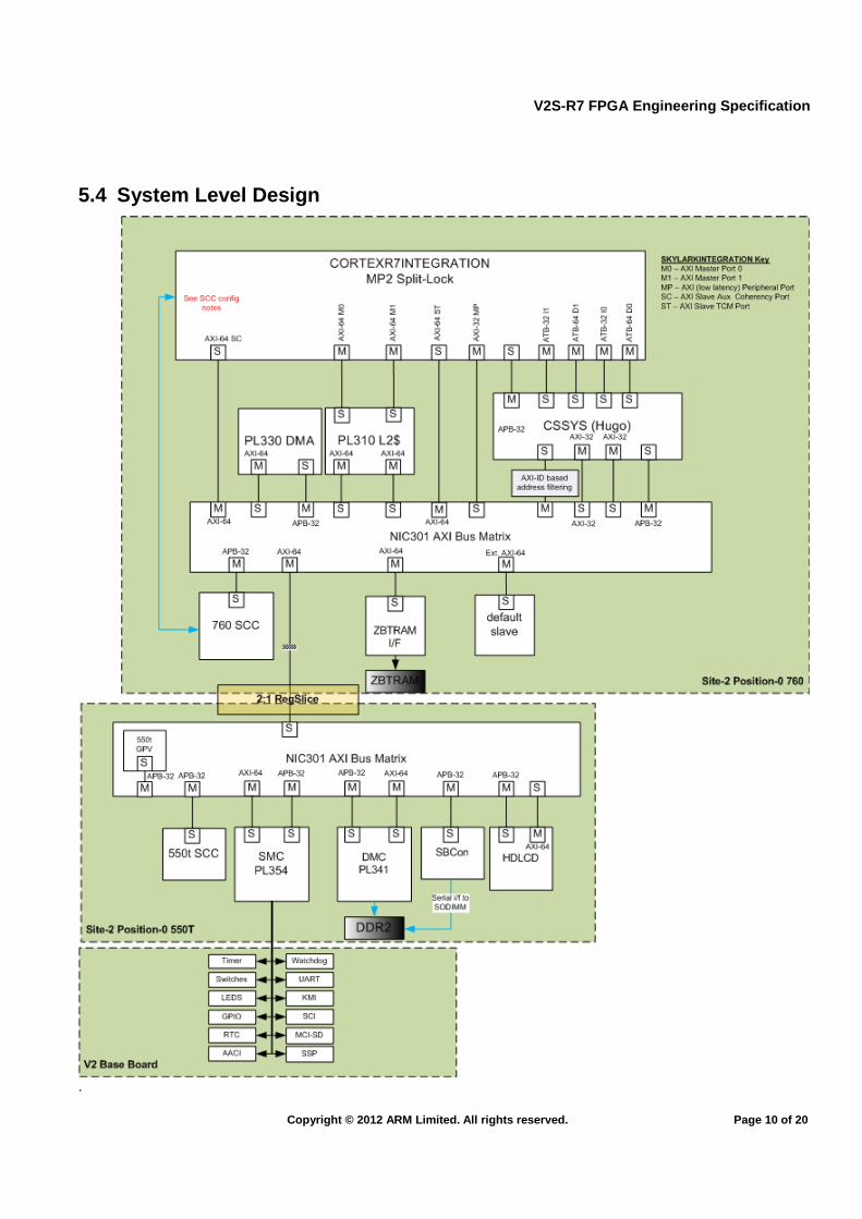
5.4 System Level Design
.
V2S-R7 FPGA Engineering Specification
Copyright © 2012 ARM Limited. All rights reserved. Page 11 of 20
Figure 2 System Level Design Partitioning
V2S-R7 FPGA Engineering Specification
Copyright © 2012 ARM Limited. All rights reserved. Page 12 of 20
This SMM has two main clock domains, the 760 domain running at 40MHz and the 550t domain running at 80MHz. The 2:1 modified reg. slice component also acts as an asynchronous bridge between the two domains. Full details of all clock domains can be found in section 5.5
The design is based on the Cortex-R7 (MP2 Split-Lock), a CoreSight sub-system together with a number of system components including:
5.4.1 PL341 Dynamic Memory Controller
This is an asynchronous PL341 implementation with modified pad interface to register all I/O signals using IO pads registers.
5.4.2 SCC controller
The SCC provides a standard serial interface to a LogicTile Express 13MG (V2F-2XV6) Daughterboard Configuration Controller (DCC). The DCC uses this interface by issuing commands to receive/transmit information from/to the SCC registers in the FPGA.
The default state of the SCC registers is determined by the DCC during the power-up phase. The DCC reads the register values from a text file on the system SD card. During runtime the SCC registers are addressable by all masters in the system.
The SCC registers provides configuration registers for system/processor control. Please refer to Table for full details of the SCC registers.
5.4.3 PL354 Static Memory Controller
This is the Static Memory Controller used to communicate with the motherboard. The ARM PrimeCell PL354 is used in this design. The SMC can be remapped using the SCC block, refer to section 6.1.
5.4.4 ACP port
The processor ACP port can be only accessed by DMA.
5.4.5 DMA controller
The DMAC provides an AXI interface to perform DMA transfers, two APB interfaces that control its operation and setup. Only one APB interface which implements TrustZone® secure technology is connected, the other is unused.
5.4.6 ZBT RAM controller
This is a bridge which converts 64 bit AXI transfers into ZBT SRAM transfers. It based on BP140 with extra AxiRegSlices on the data read site which increases performance. The ZBT SRAM operates synchronously to the AXI domain with no wait states and 2 cycles of latency.
The ZBTRAM memory only supports a read only mode. This is controlled by a control bit in SCC_SYSCFG in the SCC register block. It is targeted for testing hardware break point.
V2S-R7 FPGA Engineering Specification
Copyright © 2012 ARM Limited. All rights reserved. Page 13 of 20
5.4.7 HCLCD controller
The HDLCD controller is used to drive a monitor that can support higher resolutions.
5.4.8 L2C-310 Level 2 Cache
This SMM includes the L2C-310 level 2 cache controller.
5.4.9 CoreSight
The CoreSight Subsystem has been implemented in this SMM. Full details can be found in the section 5.2 Debug Features of this document.
5.4.10 Cortex-R7
The Cortex-R7 CPU has been implemented in an MP2 Split-Lock configuration. Details of the processor implementation can be found in section 5.1
V2S-R7 FPGA Engineering Specification
Copyright © 2012 ARM Limited. All rights reserved. Page 14 of 20
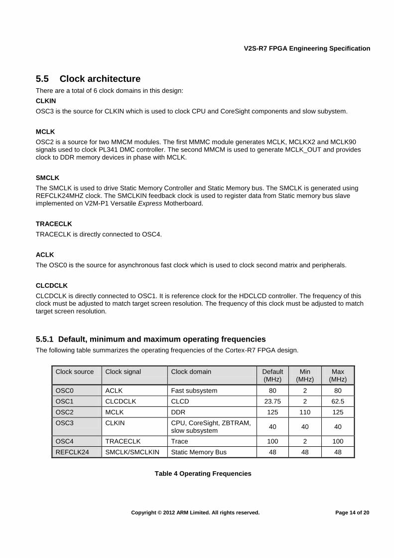
5.5 Clock architecture
There are a total of 6 clock domains in this design:
CLKIN
OSC3 is the source for CLKIN which is used to clock CPU and CoreSight components and slow subystem.
MCLK
OSC2 is a source for two MMCM modules. The first MMMC module generates MCLK, MCLKX2 and MCLK90 signals used to clock PL341 DMC controller. The second MMCM is used to generate MCLK_OUT and provides clock to DDR memory devices in phase with MCLK.
SMCLK
The SMCLK is used to drive Static Memory Controller and Static Memory bus. The SMCLK is generated using REFCLK24MHZ clock. The SMCLKIN feedback clock is used to register data from Static memory bus slave implemented on V2M-P1 Versatile Express Motherboard.
TRACECLK
TRACECLK is directly connected to OSC4.
ACLK
The OSC0 is the source for asynchronous fast clock which is used to clock second matrix and peripherals.
CLCDCLK
CLCDCLK is directly connected to OSC1. It is reference clock for the HDCLCD controller. The frequency of this clock must be adjusted to match target screen resolution. The frequency of this clock must be adjusted to match target screen resolution.
5.5.1 Default, minimum and maximum operating frequencies
The following table summarizes the operating frequencies of the Cortex-R7 FPGA design.
Clock source Clock signal Clock domain Default (MHz)
Min (MHz)
Max (MHz)
OSC0 ACLK Fast subsystem 80 2 80
OSC1 CLCDCLK CLCD 23.75 2 62.5
OSC2 MCLK DDR 125 110 125
OSC3 CLKIN CPU, CoreSight, ZBTRAM, slow subsystem
40 40 40
OSC4 TRACECLK Trace 100 2 100
REFCLK24 SMCLK/SMCLKIN Static Memory Bus 48 48 48
Table 4 Operating Frequencies
V2S-R7 FPGA Engineering Specification
Copyright © 2012 ARM Limited. All rights reserved. Page 15 of 20
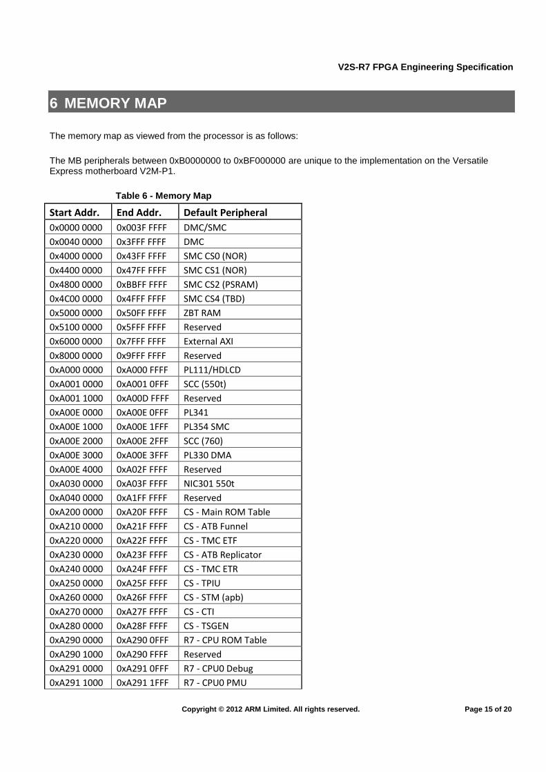
6 MEMORY MAP
The memory map as viewed from the processor is as follows:
The MB peripherals between 0xB0000000 to 0xBF000000 are unique to the implementation on the Versatile Express motherboard V2M-P1.
Table 6 - Memory Map
Start Addr. End Addr. Default Peripheral
0x0000 0000 0x003F FFFF DMC/SMC
0x0040 0000 0x3FFF FFFF DMC
0x4000 0000 0x43FF FFFF SMC CS0 (NOR)
0x4400 0000 0x47FF FFFF SMC CS1 (NOR)
0x4800 0000 0xBBFF FFFF SMC CS2 (PSRAM)
0x4C00 0000 0x4FFF FFFF SMC CS4 (TBD)
0x5000 0000 0x50FF FFFF ZBT RAM
0x5100 0000 0x5FFF FFFF Reserved
0x6000 0000 0x7FFF FFFF External AXI
0x8000 0000 0x9FFF FFFF Reserved
0xA000 0000 0xA000 FFFF PL111/HDLCD
0xA001 0000 0xA001 0FFF SCC (550t)
0xA001 1000 0xA00D FFFF Reserved
0xA00E 0000 0xA00E 0FFF PL341
0xA00E 1000 0xA00E 1FFF PL354 SMC
0xA00E 2000 0xA00E 2FFF SCC (760)
0xA00E 3000 0xA00E 3FFF PL330 DMA
0xA00E 4000 0xA02F FFFF Reserved
0xA030 0000 0xA03F FFFF NIC301 550t
0xA040 0000 0xA1FF FFFF Reserved
0xA200 0000 0xA20F FFFF CS - Main ROM Table
0xA210 0000 0xA21F FFFF CS - ATB Funnel
0xA220 0000 0xA22F FFFF CS - TMC ETF
0xA230 0000 0xA23F FFFF CS - ATB Replicator
0xA240 0000 0xA24F FFFF CS - TMC ETR
0xA250 0000 0xA25F FFFF CS - TPIU
0xA260 0000 0xA26F FFFF CS - STM (apb)
0xA270 0000 0xA27F FFFF CS - CTI
0xA280 0000 0xA28F FFFF CS - TSGEN
0xA290 0000 0xA290 0FFF R7 - CPU ROM Table
0xA290 1000 0xA290 FFFF Reserved
0xA291 0000 0xA291 0FFF R7 - CPU0 Debug
0xA291 1000 0xA291 1FFF R7 - CPU0 PMU
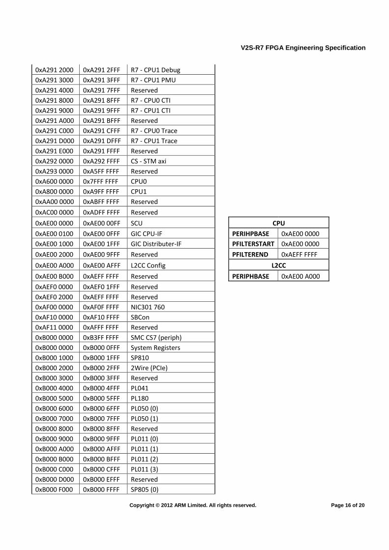
V2S-R7 FPGA Engineering Specification
Copyright © 2012 ARM Limited. All rights reserved. Page 16 of 20
0xA291 2000 0xA291 2FFF R7 - CPU1 Debug
0xA291 3000 0xA291 3FFF R7 - CPU1 PMU
0xA291 4000 0xA291 7FFF Reserved
0xA291 8000 0xA291 8FFF R7 - CPU0 CTI
0xA291 9000 0xA291 9FFF R7 - CPU1 CTI
0xA291 A000 0xA291 BFFF Reserved
0xA291 C000 0xA291 CFFF R7 - CPU0 Trace
0xA291 D000 0xA291 DFFF R7 - CPU1 Trace
0xA291 E000 0xA291 FFFF Reserved
0xA292 0000 0xA292 FFFF CS - STM axi
0xA293 0000 0xA5FF FFFF Reserved
0xA600 0000 0x7FFF FFFF CPU0
0xA800 0000 0xA9FF FFFF CPU1
0xAA00 0000 0xABFF FFFF Reserved
0xAC00 0000 0xADFF FFFF Reserved
0xAE00 0000 0xAE00 00FF SCU CPU
0xAE00 0100 0xAE00 0FFF GIC CPU-IF PERIHPBASE 0xAE00 0000
0xAE00 1000 0xAE00 1FFF GIC Distributer-IF PFILTERSTART 0xAE00 0000
0xAE00 2000 0xAE00 9FFF Reserved PFILTEREND 0xAEFF FFFF
0xAE00 A000 0xAE00 AFFF L2CC Config L2CC
0xAE00 B000 0xAEFF FFFF Reserved PERIPHBASE 0xAE00 A000
0xAEF0 0000 0xAEF0 1FFF Reserved
0xAEF0 2000 0xAEFF FFFF Reserved
0xAF00 0000 0xAF0F FFFF NIC301 760
0xAF10 0000 0xAF10 FFFF SBCon
0xAF11 0000 0xAFFF FFFF Reserved
0xB000 0000 0xB3FF FFFF SMC CS7 (periph)
0xB000 0000 0xB000 0FFF System Registers
0xB000 1000 0xB000 1FFF SP810
0xB000 2000 0xB000 2FFF 2Wire (PCIe)
0xB000 3000 0xB000 3FFF Reserved
0xB000 4000 0xB000 4FFF PL041
0xB000 5000 0xB000 5FFF PL180
0xB000 6000 0xB000 6FFF PL050 (0)
0xB000 7000 0xB000 7FFF PL050 (1)
0xB000 8000 0xB000 8FFF Reserved
0xB000 9000 0xB000 9FFF PL011 (0)
0xB000 A000 0xB000 AFFF PL011 (1)
0xB000 B000 0xB000 BFFF PL011 (2)
0xB000 C000 0xB000 CFFF PL011 (3)
0xB000 D000 0xB000 EFFF Reserved
0xB000 F000 0xB000 FFFF SP805 (0)
V2S-R7 FPGA Engineering Specification
Copyright © 2012 ARM Limited. All rights reserved. Page 17 of 20
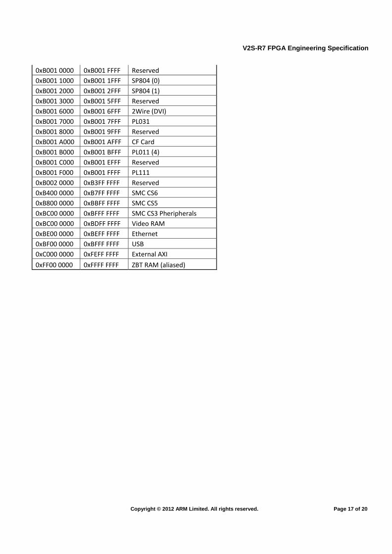
0xB001 0000 0xB001 FFFF Reserved
0xB001 1000 0xB001 1FFF SP804 (0)
0xB001 2000 0xB001 2FFF SP804 (1)
0xB001 3000 0xB001 5FFF Reserved
0xB001 6000 0xB001 6FFF 2Wire (DVI)
0xB001 7000 0xB001 7FFF PL031
0xB001 8000 0xB001 9FFF Reserved
0xB001 A000 0xB001 AFFF CF Card
0xB001 B000 0xB001 BFFF PL011 (4)
0xB001 C000 0xB001 EFFF Reserved
0xB001 F000 0xB001 FFFF PL111
0xB002 0000 0xB3FF FFFF Reserved
0xB400 0000 0xB7FF FFFF SMC CS6
0xB800 0000 0xBBFF FFFF SMC CS5
0xBC00 0000 0xBFFF FFFF SMC CS3 Pheripherals
0xBC00 0000 0xBDFF FFFF Video RAM
0xBE00 0000 0xBEFF FFFF Ethernet
0xBF00 0000 0xBFFF FFFF USB
0xC000 0000 0xFEFF FFFF External AXI
0xFF00 0000 0xFFFF FFFF ZBT RAM (aliased)
V2S-R7 FPGA Engineering Specification
Copyright © 2012 ARM Limited. All rights reserved. Page 18 of 20
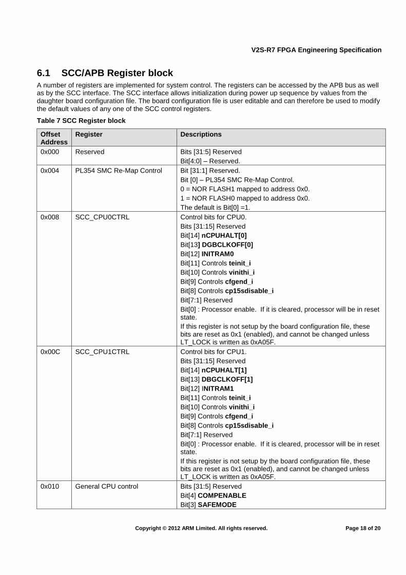
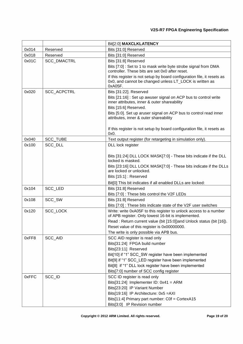
6.1 SCC/APB Register block
A number of registers are implemented for system control. The registers can be accessed by the APB bus as well as by the SCC interface. The SCC interface allows initialization during power up sequence by values from the daughter board configuration file. The board configuration file is user editable and can therefore be used to modify the default values of any one of the SCC control registers.
Table 7 SCC Register block
Offset Address
Register Descriptions
0x000 Reserved Bits [31:5] Reserved
Bit[4:0] – Reserved.
0x004 PL354 SMC Re-Map Control Bit [31:1] Reserved.
Bit [0] – PL354 SMC Re-Map Control.
0 = NOR FLASH1 mapped to address 0x0.
1 = NOR FLASH0 mapped to address 0x0.
The default is Bit[0] =1.
0x008 SCC_CPU0CTRL Control bits for CPU0.
Bits [31:15] Reserved
Bit[14] nCPUHALT[0]
Bit[13] DGBCLKOFF[0]
Bit[12] INITRAM0
Bit[11] Controls teinit_i
Bit[10] Controls vinithi_i
Bit[9] Controls cfgend_i
Bit[8] Controls cp15sdisable_i
Bit[7:1] Reserved
Bit[0] : Processor enable. If it is cleared, processor will be in reset state.
If this register is not setup by the board configuration file, these bits are reset as 0x1 (enabled), and cannot be changed unless LT_LOCK is written as 0xA05F.
0x00C SCC_CPU1CTRL Control bits for CPU1.
Bits [31:15] Reserved
Bit[14] nCPUHALT[1]
Bit[13] DBGCLKOFF[1]
Bit[12] INITRAM1
Bit[11] Controls teinit_i
Bit[10] Controls vinithi_i
Bit[9] Controls cfgend_i
Bit[8] Controls cp15sdisable_i
Bit[7:1] Reserved
Bit[0] : Processor enable. If it is cleared, processor will be in reset state.
If this register is not setup by the board configuration file, these bits are reset as 0x1 (enabled), and cannot be changed unless LT_LOCK is written as 0xA05F.
0x010 General CPU control Bits [31:5] Reserved
Bit[4] COMPENABLE
Bit[3] SAFEMODE
V2S-R7 FPGA Engineering Specification
Copyright © 2012 ARM Limited. All rights reserved. Page 19 of 20
Bit[2:0] MAXCLKLATENCY
0x014 Reserved Bits [31:0] Reserved
0x018 Reserved Bits [31:0] Reserved
0x01C SCC_DMACTRL Bits [31:8] Reserved
Bits [7:0] : Set to 1 to mask write byte strobe signal from DMA controller. These bits are set 0x0 after reset.
If this register is not setup by board configuration file, it resets as 0x0, and cannot be changed unless LT_LOCK is written as 0xA05F.
0x020 SCC_ACPCTRL Bits [31:22]. Reserved
Bits [21:16] : Set up awuser signal on ACP bus to control write inner attributes, inner & outer shareability
Bits [15:6] Reserved.
Bits [5:0]. Set up aruser signal on ACP bus to control read inner attributes, inner & outer shareability
If this register is not setup by board configuration file, it resets as 0x0.
0x040 SCC_TUBE Text output register (for retargeting in simulation only).
0x100 SCC_DLL DLL lock register
Bits [31:24] DLL LOCK MASK[7:0] - These bits indicate if the DLL locked is masked.
Bits [23:16] DLL LOCK MASK[7:0] - These bits indicate if the DLLs are locked or unlocked.
Bits [15:1] : Reserved
Bit[0] This bit indicates if all enabled DLLs are locked:
0x104 SCC_LED Bits [31:8] Reserved
Bits [7:0] : These bits control the V2F LEDs
0x108 SCC_SW Bits [31:8] Reserved
Bits [7:0] : These bits indicate state of the V2F user switches
0x120 SCC_LOCK Write: write 0xA05F to this register to unlock access to a number of APB register. Only lowest 16-bit is implemented.
Read : Return current value (bit [15:0])and Unlock status (bit [16]).
Reset value of this register is 0x00000000.
The write is only possible via APB bus.
0xFF8 SCC_AID SCC AID register is read only
Bits[31:24] FPGA build number
Bits[23:11] Reserved
Bit[10] if “1” SCC_SW register have been implemented
Bit[9] if “1” SCC_LED register have been implemented
Bit[8] if “1” DLL lock register have been implemented
Bits[7:0] number of SCC config register
0xFFC SCC_ID SCC ID register is read only
Bits[31:24] Implementer ID: 0x41 = ARM
Bits[23:20] IP Variant Number
Bits[19:16] IP Architecture: 0x5 =AXI
Bits[11:4] Primary part number: C0f = CortexA15
Bits[3:0] IP Revision number
V2S-R7 FPGA Engineering Specification
Copyright © 2012 ARM Limited. All rights reserved. Page 20 of 20
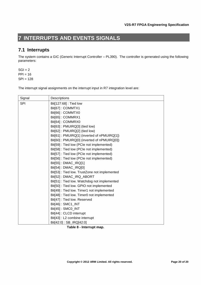
7 INTERRUPTS AND EVENTS SIGNALS
7.1 Interrupts
The system contains a GIC (Generic Interrupt Controller – PL390). The controller is generated using the following parameters:
SGI = 2
PPI = 16
SPI = 128
The interrupt signal assignments on the interrupt input in R7 integration level are:
Signal Descriptions
SPI Bit[127:68] : Tied low
Bit[67] : COMMTX1
Bit[66] : COMMTX0
Bit[65] : COMMRX1
Bit[64] : COMMRX0
Bit[63] : PMUIRQ[3] (tied low)
Bit[62] : PMUIRQ[2] (tied low)
Bit[61] : PMUIRQ[1] (inverted of nPMUIRQ[1])
Bit[60] : PMUIRQ[0] (inverted of nPMUIRQ[0])
Bit[59] : Tied low (PCIe not implemented)
Bit[58] : Tied low (PCIe not implemented)
Bit[57] : Tied low (PCIe not implemented)
Bit[56] : Tied low (PCIe not implemented)
Bit[55] : DMAC_IRQ[1]
Bit[54] : DMAC_IRQ[0]
Bit[53] : Tied low. TrustZone not implemented
Bit[52] : DMAC_IRQ_ABORT
Bit[51] : Tied low. Watchdog not implemented
Bit[50] : Tied low. GPIO not implemented
Bit[49] : Tied low. Timer1 not implemented
Bit[48] : Tied low. Timer0 not implemented
Bit[47] : Tied low. Reserved
Bit[46] : SMC1_INT
Bit[45] : SMC0_INT
Bit[44] : CLCD interrupt
Bit[43] : L2 combine interrupt
Bit[42:0] : SB_IRQ[42:0]
Table 8 - Interrupt map.


![(GJH &RJQLWLYH 6ROXWLRQV ZLWK 0LFURVRIW ,R7easdam.blob.core.windows.net/iotinaction...,r7 (gjh,r7 $]xuh 6skhuh26,r7:lqgrzv ,r7 /lqx[$]xuh,r7 (gjh &rpsdwleoh zlwk srsxodu rshudwlqj](https://img.pdfslide.us/doc/110x75/5f8df0458c541e24040c3752/gjh-rjqlwlyh-6roxwlrqv-zlwk-0lfurvriw-r7-gjhr7-xuh-6skhuh26r7lqgrzv.jpg)