Embed Size (px)
Citation preview
Application Note AC359
SmartFusion Board Design Guidelines
Table of Contents
ObjectiveThe successful design of printed circuit boards (PCBs) incorporating the SmartFusion™ mixed-signalFPGA requires a good understanding of the mixed-signal nature of the SmartFusion chips. Good boarddesign practices are required to achieve the expected performance from the PCB and SmartFusiondevice. These are essential to achieve high quality and reliable results, such as minimal noise levels andadequate isolation between digital and analog domain.
This document presents guidelines for board-level design specific applications using SmartFusionmixed-signal FPGAs. These guidelines should be treated as a supplement to standard board-leveldesign practices.
This document assumes that the readers are experienced in digital and analog board layout andknowledgeable in the electrical characteristics of mixed-signal systems. Background information on thekey theories and concepts of mixed-signal board-level design is available in High Speed Digital Design:A Handbook of Black Magic1, as well as in many reference text books and literature.
Analog and Digital Plane IsolationSince SmartFusion is a mixed-signal product in which both analog and digital components exist, itrequires both analog and digital supply and ground planes. In addition, there are several voltage supplyand ground pins on the device to power different components on the die. This section discusses thelayout of the different analog or digital planes and recommends schemes to efficiently isolate differentdigital and analog domains from each other. This section also describes all ground and supply pins of theSmartFusion device required to operate the chip, and explains how to connect them to the existing digitalor analog supply or ground planes.
Placement of SmartFusion Device and Isolation of Ground PlanesIn applications using SmartFusion devices, two separate grounds to the device should be provided: GND(digital ground) and GNDA (analog ground). The ground pins of the device are to be connected to one ofthe ground planes appropriately, as discussed in the "Isolation of Ground Planes" on page 3. GND is thedigital ground plane that connects to all GND pins of a SmartFusion device, while GNDA is the analogground plane that connects to all GNDA pins of a SmartFusion device.
Objective . . . . . . . . . . . . . . . . . . . . . . . . . . . . . . . . . . . . . . . . . . . . . . . . . 1Analog and Digital Plane Isolation . . . . . . . . . . . . . . . . . . . . . . . . . . . . . . . . . . . . 1Other Special Function Pins . . . . . . . . . . . . . . . . . . . . . . . . . . . . . . . . . . . . . . . 6Application-Specific Recommendations . . . . . . . . . . . . . . . . . . . . . . . . . . . . . . . . 14List of Changes . . . . . . . . . . . . . . . . . . . . . . . . . . . . . . . . . . . . . . . . . . . . . 16
1. Johnson, Howard, and Martin Graham, High Speed Digital Design: A Handbook of Black Magic. Prentice Hall PTR, 1993.ISBN-10 0133957241 or ISBN-13: 978-0133957242
April 2011 1
© 2011 Microsemi Corporation
SmartFusion Board Design Guidelines
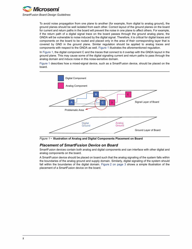
To avoid noise propagation from one plane to another (for example, from digital to analog ground), theground planes should be well isolated from each other. Correct layout of the ground planes on the boardfor current and return paths in the board will prevent the noise in one plane to affect others. For example,if the return path of a digital signal trace on the board passes through the ground analog plane, theGNDA will be vulnerable to noise induced by the digital signal. Therefore, it is critical for digital traces andcomponents on the board to be routed and placed only in the area of their corresponding layer that iscovered by GND in the ground plane. Similar regulation should be applied to analog traces andcomponents with respect to the GNDA as well. Figure 1 illustrates the aforementioned regulation.
In Figure 1, the digital component C and the traces that connect to it overlap with the GNDA layout in theground plane. This may cause some of the digital signaling current and return paths to pass through theanalog domain and induce noise in this noise-sensitive domain.
Figure 1 describes how a mixed-signal device, such as a SmartFusion device, should be placed on theboard.
Placement of SmartFusion Device on BoardSmartFusion devices contain both analog and digital components and can interface with other digital andanalog components on the board.
A SmartFusion device should be placed on board such that the analog signaling of the system falls withinthe boundaries of the analog ground and supply domain. Similarly, digital signaling of the system shouldfall within the boundaries of the digital domain. Figure 2 on page 3 shows a simple illustration of theplacement of a SmartFusion device on the board.
Figure 1 • Illustration of Analog and Digital Components Placement on Board
B
A C D
E
Digital Component
Analog Component
Signal Layer of Board
Ground Layer of Board
Problematic Area
DigitalGround
AnalogGround
2
Analog and Digital Plane Isolation
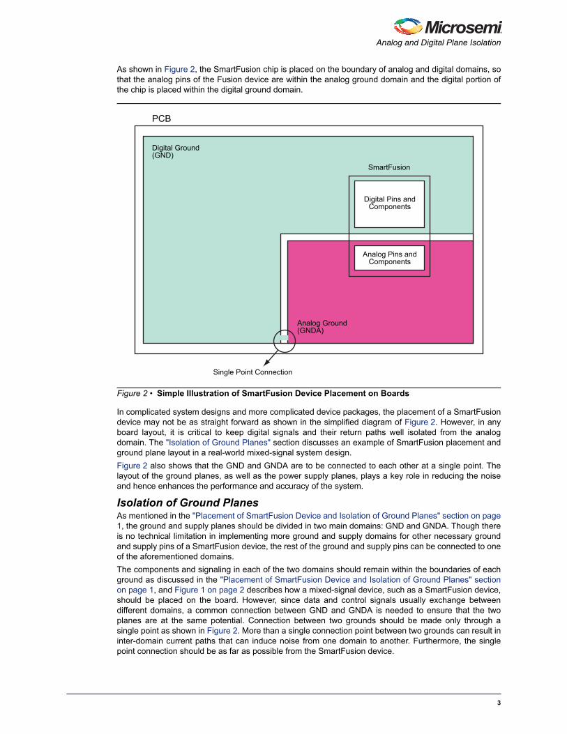
As shown in Figure 2, the SmartFusion chip is placed on the boundary of analog and digital domains, sothat the analog pins of the Fusion device are within the analog ground domain and the digital portion ofthe chip is placed within the digital ground domain.
In complicated system designs and more complicated device packages, the placement of a SmartFusiondevice may not be as straight forward as shown in the simplified diagram of Figure 2. However, in anyboard layout, it is critical to keep digital signals and their return paths well isolated from the analogdomain. The "Isolation of Ground Planes" section discusses an example of SmartFusion placement andground plane layout in a real-world mixed-signal system design.
Figure 2 also shows that the GND and GNDA are to be connected to each other at a single point. Thelayout of the ground planes, as well as the power supply planes, plays a key role in reducing the noiseand hence enhances the performance and accuracy of the system.
Isolation of Ground PlanesAs mentioned in the "Placement of SmartFusion Device and Isolation of Ground Planes" section on page1, the ground and supply planes should be divided in two main domains: GND and GNDA. Though thereis no technical limitation in implementing more ground and supply domains for other necessary groundand supply pins of a SmartFusion device, the rest of the ground and supply pins can be connected to oneof the aforementioned domains.
The components and signaling in each of the two domains should remain within the boundaries of eachground as discussed in the "Placement of SmartFusion Device and Isolation of Ground Planes" sectionon page 1, and Figure 1 on page 2 describes how a mixed-signal device, such as a SmartFusion device,should be placed on the board. However, since data and control signals usually exchange betweendifferent domains, a common connection between GND and GNDA is needed to ensure that the twoplanes are at the same potential. Connection between two grounds should be made only through asingle point as shown in Figure 2. More than a single connection point between two grounds can result ininter-domain current paths that can induce noise from one domain to another. Furthermore, the singlepoint connection should be as far as possible from the SmartFusion device.
Figure 2 • Simple Illustration of SmartFusion Device Placement on Boards
Single Point Connection
PCB
Analog Ground(GNDA)
Analog Pins andComponents
Digital Pins andComponents
Digital Ground(GND)
SmartFusion
3
SmartFusion Board Design Guidelines
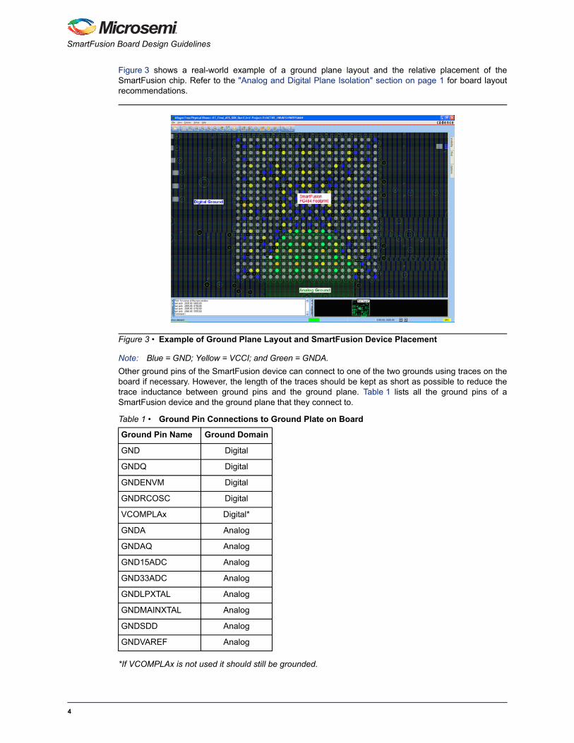
Figure 3 shows a real-world example of a ground plane layout and the relative placement of theSmartFusion chip. Refer to the "Analog and Digital Plane Isolation" section on page 1 for board layoutrecommendations.
Note: Blue = GND; Yellow = VCCI; and Green = GNDA.
Other ground pins of the SmartFusion device can connect to one of the two grounds using traces on theboard if necessary. However, the length of the traces should be kept as short as possible to reduce thetrace inductance between ground pins and the ground plane. Table 1 lists all the ground pins of aSmartFusion device and the ground plane that they connect to.
*If VCOMPLAx is not used it should still be grounded.
Figure 3 • Example of Ground Plane Layout and SmartFusion Device Placement
Table 1 • Ground Pin Connections to Ground Plate on Board
Ground Pin Name Ground Domain
GND Digital
GNDQ Digital
GNDENVM Digital
GNDRCOSC Digital
VCOMPLAx Digital*
GNDA Analog
GNDAQ Analog
GND15ADC Analog
GND33ADC Analog
GNDLPXTAL Analog
GNDMAINXTAL Analog
GNDSDD Analog
GNDVAREF Analog
4
Analog and Digital Plane Isolation
Analog and Digital Voltage Supply IsolationDigital and analog voltage supplies should be isolated from each other similar to the grounds asdiscussed in the "Placement of SmartFusion Device and Isolation of Ground Planes" section on page 1.There are four main power supplies to SmartFusion devices: VCC33A (3.3 V analog supply), VCC15A(1.5 V analog supply), VCC (1.5 V digital core supply), and VCCI (digital I/O supply). There may bemultiple VCCI levels (for digital I/Os) since SmartFusion devices offer multiple I/O banks. Regardless ofthe number of power supply voltage levels, the layout of the board's power plans should conform to thesame specifications as recommended for the ground plane in the "Placement of SmartFusion Device andIsolation of Ground Planes" section on page 1.
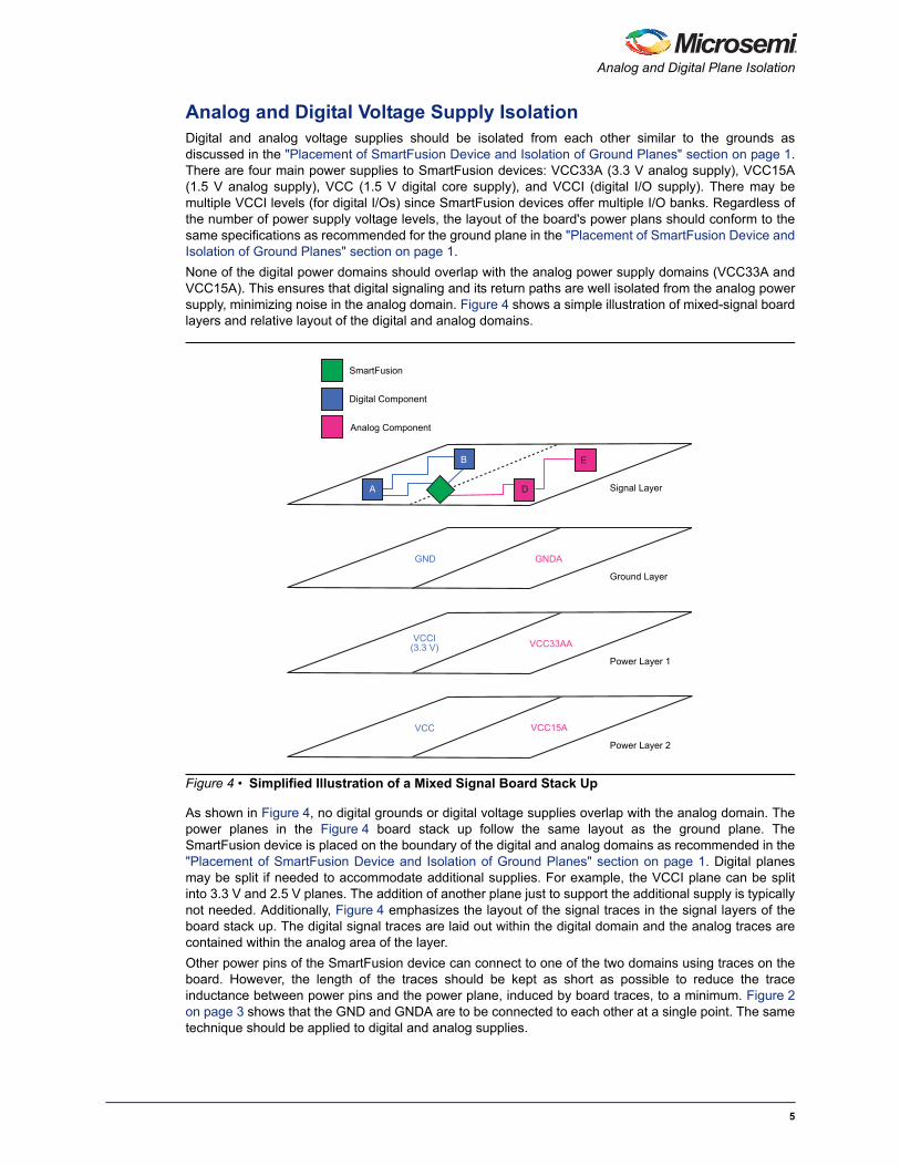
None of the digital power domains should overlap with the analog power supply domains (VCC33A andVCC15A). This ensures that digital signaling and its return paths are well isolated from the analog powersupply, minimizing noise in the analog domain. Figure 4 shows a simple illustration of mixed-signal boardlayers and relative layout of the digital and analog domains.
As shown in Figure 4, no digital grounds or digital voltage supplies overlap with the analog domain. Thepower planes in the Figure 4 board stack up follow the same layout as the ground plane. TheSmartFusion device is placed on the boundary of the digital and analog domains as recommended in the"Placement of SmartFusion Device and Isolation of Ground Planes" section on page 1. Digital planesmay be split if needed to accommodate additional supplies. For example, the VCCI plane can be splitinto 3.3 V and 2.5 V planes. The addition of another plane just to support the additional supply is typicallynot needed. Additionally, Figure 4 emphasizes the layout of the signal traces in the signal layers of theboard stack up. The digital signal traces are laid out within the digital domain and the analog traces arecontained within the analog area of the layer.
Other power pins of the SmartFusion device can connect to one of the two domains using traces on theboard. However, the length of the traces should be kept as short as possible to reduce the traceinductance between power pins and the power plane, induced by board traces, to a minimum. Figure 2on page 3 shows that the GND and GNDA are to be connected to each other at a single point. The sametechnique should be applied to digital and analog supplies.
Figure 4 • Simplified Illustration of a Mixed Signal Board Stack Up
B
A D
E
Digital Component
SmartFusion
Analog Component
Signal Layer
Ground Layer
GND GNDA
Power Layer 1
VCCI(3.3 V) VCC33AA
Power Layer 2
VCC VCC15A
5
SmartFusion Board Design Guidelines
Table 2 lists all the power pins of a SmartFusion device and the power plane that they connect to.
Notes:
1. Can be tied to any digital 3.3 V rail available in the application board (for example, VCCFPGAIOBx if thebank requires a 3.3 V supply).
2. If multiple banks are powered with different supply levels, different VCCI planes are needed for eachvoltage level.
3. Capacitor recommendations for VCCPLLx pins are similar to those for the ProASIC3 family device and canbe found at www.actel.com/documents/PA3_UG.pdf.
Similar to any other board-level designs, decoupling/bypass capacitors or other power supply filteringtechniques should be used between power supply pins and the ground to reduce any potential fluctuationon the supply lines. The SoC Products Group recommends that a 33nH inductor be placed between thesupply source and a 0.1 uF capacitor to filter out any low-/medium- and high-frequency noise for theVCCRCOSC supply input. For additional recommendations in using decoupling capacitors, refer to theBoard-Level Considerations application note. There are numerous other industry publications andguidelines available on the subject.
Other Special Function PinsIn addition to the general power and ground pins discussed in the "Analog and Digital Plane Isolation"section on page 1, there are a few other special pins that require special board considerations to ensureproper functionality of the SmartFusion device. This section of the document lists these pins anddescribes their connectivity in the board-level design.
Table 2 • Power Pin Connections to Power Plane on Board
Supply Pin Name
Supply Domain
SupplyVoltage Level Handling When Unused
VCC Digital 1.5 V Powered all the time
VCCENVM Digital 1.5 V Powered all the time
VCCRCOSC1 Digital 3.3 V Powered all the time
VCCMSSIOBx1 Digital 3.3 V Grounded if IO Bank x is unused
VCCFPGAIOBx2 Digital 1.5 V Grounded if IO Bank x is unused
VCCPLLx3 Digital (connectrecommended
capacitors)
1.5 V Powered all the time
VCC15A Analog 1.5 V Powered all the time
VCC15ADC Analog 1.5 V Powered all the time
VCC33A Analog 3.3 V Powered all the time
VCC33ADC Analog 3.3 V Either pull down or connect to VCC33A
VCC33AP Analog 3.3 V Can be left floating or connect to VCC33A
VCC33SDD0 Analog 3.3 V Floating or connect to VCC33A if DAC0 is unused
VCC33SDD1 Analog 3.3 V Floating or connect to VCC33A if DAC1 and DAC2 areunused
VCCLPXTAL Analog 3.3 V Powered all the time
VCCMAINXTAL Analog 3.3 V Grounded if unused
6

Other Special Function Pins
VAREFxThere are up to three pins: VAREF0, VAREF1, and VAREF2 that provide the voltage reference forSmartFusion’s analog-to-digital converter (ADC). VAREF2 is available only in the A2F500 device. TheSmartFusion device can be configured to generate a 2.56 V internal reference that can be used by theADC. While using the internal reference, the reference voltage is output on the VAREFOUT pin for useas a system reference.
When VAREF0 is internally generated, a bypass capacitor must be connected from this pin to GNDA.The value of the bypass capacitor should be between 3.3 µF and 22 µF, which is based on the needs ofthe individual design. The above range of capacitor values supports the accuracy specification of theADC, which is detailed in the datasheet. The choice of the capacitor value has an impact on the settlingtime of the VAREF0 signal to reach the required specification of 2.56 V to initiate valid conversions by theADC. If the lower capacitor value is chosen, the settling time required for VAREF0 to achieve 2.56 V willbe shorter than when selecting the larger capacitor value.
Designers choosing the smaller capacitor value will not obtain as much margin in the accuracy as thatachieved with a larger capacitor value. The choice of capacitor values also depends on the total amountof noise existing on the user’s board. Boards with relatively higher noise levels may need to havecapacitor values close to 22 µF. On the other hand, the VAREF pin may not perform as expected if thecapacitor values are close to 3.3 µF. See the ADC section in the SmartFusion Programmable AnalogUser’s Guide for more information.
The SoC Products Group recommends using 10 µF as the value of the bypass capacitor. To use theinternal voltage reference, you must connect the VAREFOUT pin to the appropriate ADC VAREFxinput—either the VAREF0 or VAREF1 pin—on the PCB.
If a different reference voltage is required, it can be supplied using an external source between thecorresponding VAREFx pin and GNDVAREF pin. The valid range of values that can be supplied to theADC is 1.0 V to 3.3 V. Designers choosing to use an external VAREFx need to ensure that a stable andclean VAREFx source is supplied to the VAREFx pin before initiating conversions by the ADCx.
Since VAREF is the reference voltage for the ADC, it is critical for VAREF (either internal or external) tobe very clean. Noise on VAREF affects the accuracy of the ADC and may cause the analog system tooperate outside the specification listed in the SmartFusion Intelligent Mixed-Signal FPGAs datasheet.For internal VAREF use model, the SoC Products Group recommends the external capacitor to beplaced between VAREF and the analog ground, as close as possible to the VAREF pin. If these VAREFand VAREFOUT pins are not used, then these can be left floating.
VCC33N, PCAP, and NCAPThese three pins are associated with the -3.3 V charge pump. This charge pump uses two externalcapacitors in order to generate the -3.3 V supply. One capacitor is connected between the NCAP andPCAP pins, while the other is connected between VCC33N and the analog ground. The impulse chargingof the capacitors, while the charge pump is in operation, is a source of electromagnetic interference(EMI). To reduce EMI, each of these capacitors consists of a 0.1 µF ceramic capacitor in parallel with atantalum capacitor. The ceramic capacitors should be mounted as close as possible to the pins, usingcapacitors of small physical size. For the BGA package, these capacitors are to be mounted on thebottom layer, directly underneath the respective pins. The tantalum capacitors can be mounted a littlefurther off, but you should try to minimize the distance. Ceramic capacitors are also available in highervalues such as 2.2 µF. If such a capacitor is used, the 0.1 µF capacitor might not be needed. If the analogblock is not used, then these pins can be left floating.
MAINXIN and MAINXOUTMAINXIN is an input from an external crystal, ceramic resonator, or RC network, while MAINXOUT is anoutput to the same crystal. When using an external crystal or ceramic resonator, external capacitors arerecommended, which will depend on the crystal oscillator manufacturer. If using an external RC networkor clock input, MAINXIN should be used and MAINXOUT should be left unconnected.
7
SmartFusion Board Design Guidelines
For the layout and connection of the external crystal and the associated capacitors, keep straycapacitance and inductance to a minimum. It is very important to keep any noise from coupling to the on-chip crystal oscillator by way of power supply, the crystal, the two load capacitors, or the copper tracesused to connect these components. It is also important to prevent noise from coupling from the oscillatorinto the analog power supply, thus affecting the performance and accuracy of other analog circuitry.
The following guidelines help achieve these objectives:
• The crystal should be placed as close as possible to the MAINXIN and MAINXOUT pins.
• The spacing between traces connecting crystal to MAINXIN and MAINXOUT pins and nearbytraces should be increased beyond the minimum spacing dictated by the PCB design rules toprevent any noise from coupling into these traces. In addition, copper traces carrying high speeddigital signals should not be routed in parallel to the copper traces connected to the MAINXIN andMAINXOUT pins, either on the same layer or on the other layers.
• To reduce electromagnetic emissions and provide good mechanical stability to the crystal, acopper pad slightly larger than the crystal and grounded to GNDMAINXTAL should be placed onthe top layer of the PCB. The metal package of the crystal should be grounded to this pad with asuitable clip. Copper traces connected to this grounded pad and extending around the coppertraces leading from the crystal to MAINXIN and MAINXOUT pins shield these pins and furtherincrease noise immunity of the oscillator. The shields add a very small amount of straycapacitance and this can be accounted for in the selection of the load capacitors.
The main crystal oscillator can be connected in two ways:
• RC-oscillator mode
• External crystal or Ceramic resonator mode
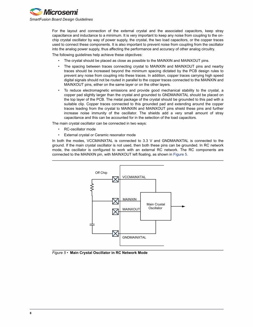
In both the modes, VCCMAINXTAL is connected to 3.3 V and GNDMAINXTAL is connected to theground. If the main crystal oscillator is not used, then both these pins can be grounded. In RC networkmode, the oscillator is configured to work with an external RC network. The RC components areconnected to the MAINXIN pin, with MAINXOUT left floating, as shown in Figure 5.
Figure 5 • Main Crystal Oscillator in RC Network Mode
Main CrystalOscillator
GNDMAINXTAL
VCCMAINXTAL
MAINXIN
MAINXOUT
Off Chip
8
Other Special Function Pins
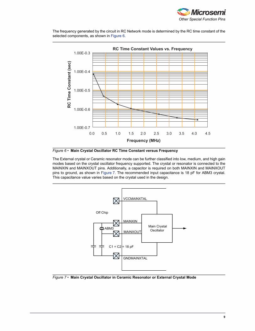
The frequency generated by the circuit in RC Network mode is determined by the RC time constant of theselected components, as shown in Figure 6.
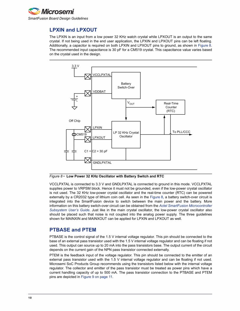
The External crystal or Ceramic resonator mode can be further classified into low, medium, and high gainmodes based on the crystal oscillator frequency supported. The crystal or resonator is connected to theMAINXIN and MAINXOUT pins. Additionally, a capacitor is required on both MAINXIN and MAINXOUTpins to ground, as shown in Figure 7. The recommended input capacitance is 18 pF for ABM3 crystal.This capacitance value varies based on the crystal used in the design.
Figure 6 • Main Crystal Oscillator RC Time Constant versus Frequency
Figure 7 • Main Crystal Oscillator in Ceramic Resonator or External Crystal Mode
0.0
1.00E-0.7
1.00E-0.6
1.00E-0.5
1.00E-0.4
1.00E-0.3
0.5 1.0 1.5 2.0 2.5 3.0 3.5 4.0 4.5
RC
Tim
e C
on
stan
t (s
ec)
Frequency (MHz)
RC Time Constant Values vs. Frequency
Main CrystalOscillator
GNDMAINXTAL
VCCMAINXTAL
MAINXIN
MAINXOUT
C1 = C2 = 18 pF
Off Chip
ABM3
9
SmartFusion Board Design Guidelines
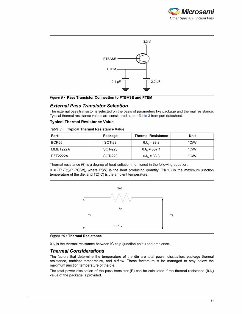
LPXIN and LPXOUTThe LPXIN is an input from a low power 32 KHz watch crystal while LPXOUT is an output to the samecrystal. If not being used in the end user application, the LPXIN and LPXOUT pins can be left floating.Additionally, a capacitor is required on both LPXIN and LPXOUT pins to ground, as shown in Figure 8.The recommended input capacitance is 30 pF for a CM519 crystal. This capacitance value varies basedon the crystal used in the design.
VCCLPXTAL is connected to 3.3 V and GNDLPXTAL is connected to ground in this mode. VCCLPXTALsupplies power to VRPSM block. Hence it must not be grounded, even if the low-power crystal oscillatoris not used. The 32 KHz low-power crystal oscillator and the real-time counter (RTC) can be poweredexternally by a CR2032 type of lithium coin cell. As seen in the Figure 8, a battery switch-over circuit isintegrated into the SmartFusion device to switch between the main power and the battery. Moreinformation on this battery switch-over circuit can be obtained from the Actel SmartFusion MicrocontrollerSubsystem User’s Guide. Just like in the main crystal oscillator, the low-power crystal oscillator alsoshould be placed such that noise is not coupled into the analog power supply. The three guidelinesshown for MAINXIN and MAINXOUT can be applied for LPXIN and LPXOUT as well.
PTBASE and PTEMPTBASE is the control signal of the 1.5 V internal voltage regulator. This pin should be connected to thebase of an external pass transistor used with the 1.5 V internal voltage regulator and can be floating if notused. This output can source up to 20 mA into the pass transistors base. The output current of the circuitdepends on the current gain of the NPN pass transistor connected externally.
PTEM is the feedback input of the voltage regulator. This pin should be connected to the emitter of anexternal pass transistor used with the 1.5 V internal voltage regulator and can be floating if not used.Microsemi SoC Products Group recommends using the transistors listed below with the internal voltageregulator. The collector and emitter of the pass transistor must be treated as power pins which have acurrent handling capacity of up to 500 mA. The pass transistor connection to the PTBASE and PTEMpins are depicted in Figure 9 on page 11.
Figure 8 • Low Power 32 KHz Oscillator with Battery Switch and RTC
LP 32 KHz CrystalOscillator
GNDLPXTAL
VCCLPXTAL
LPXIN
LPXOUT
C1 = C2 = 30 pF
CM519
BatterySwitch-Over
VDDBAT
VOUT Real-TimeCounter(RTC)
To PLL/CCC
Off Chip
3.3 V
+
–
10
Other Special Function Pins
External Pass Transistor SelectionThe external pass transistor is selected on the basis of parameters like package and thermal resistance.Typical thermal resistance values are considered as per Table 3 from part datasheet.
Typical Thermal Resistance Value
Thermal resistance (θ) is a degree of heat radiation mentioned in the following equation:
θ = (T1-T2)/P (°C/W), where P(W) is the heat producing quantity, T1(°C) is the maximum junctiontemperature of the die, and T2(°C) is the ambient temperature.
θJA is the thermal resistance between IC chip (junction point) and ambience.
Thermal ConsiderationsThe factors that determine the temperature of the die are total power dissipation, package thermalresistance, ambient temperature, and airflow. These factors must be managed to stay below themaximum junction temperature of the die.
The total power dissipation of the pass transistor (P) can be calculated if the thermal resistance (θJA)value of the package is provided.
Figure 9 • Pass Transistor Connection to PTBASE and PTEM
Table 3 • Typical Thermal Resistance Value
Part Package Thermal Resistance Unit
BCP55 SOT-23 θJA = 83.3 °C/W
MMBT222A SOT-223 θJA = 357.1 °C/W
PZT2222A SOT-223 θJA = 83.3 °C/W
Figure 10 • Thermal Resistance
3.3 V
PTBASE
PTEM
0.1 μF 2.2 μF
P(W)
Rp
T1 T2
T1 > T2
11
SmartFusion Board Design Guidelines
The equation below shows the maximum power dissipation (P) that can be achieved by a given package.Exceeding this power budget would result in reliability issues on the part of the die of the package, as perequation:
P = (Tj - Ta)/ θJA
As an example of the thermal analysis procedure in design, transistor PZT2222AT1 is considered.
• Thermal resistance of SOT-223 θJA = 83.3 °C/W
• Junction Temperature = 150 °C
• Ambient temperature = 85 °C
The maximum power dissipation, Pd = (150 °C - 85 °C) / (83.3 °C/W) = 780 mW.
Redundant InformationFrom the above equations calculated for pass transistor power dissipation, one can calculate the totalcurrent of A2F 1.5 V current (Ipass) as per the equation:
Maximum Id current = Pd / Vce
• Pd: Maximum power dissipation for a given package
• Vce: Max Pass Transistor Collector-to-Emitter Voltage
Based on the above:
Ipass = 780 mW / (3.45-1.5) V = 400 mA
Based on the above calculation, we can conclude that a maximum current of 400 mA can be sourcedusing the PZ2222A device in the SOT-223 package. If the required current is greater than 400 mA, theneither a heat sink should be used or a different package/device with a lower thermal resistance should beidentified.
RecommendationsYou are advised to select appropriate packages based on the thermal calculations shown above, so thatthe maximum junction temperature does not exceed absolute maximum rating or add provision foradding a heat sink on the device.
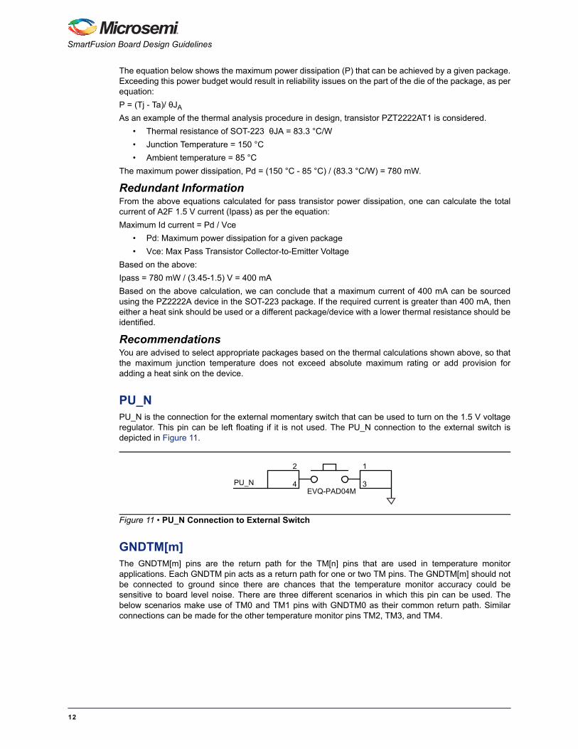
PU_NPU_N is the connection for the external momentary switch that can be used to turn on the 1.5 V voltageregulator. This pin can be left floating if it is not used. The PU_N connection to the external switch isdepicted in Figure 11.
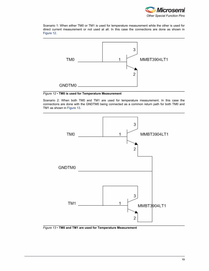
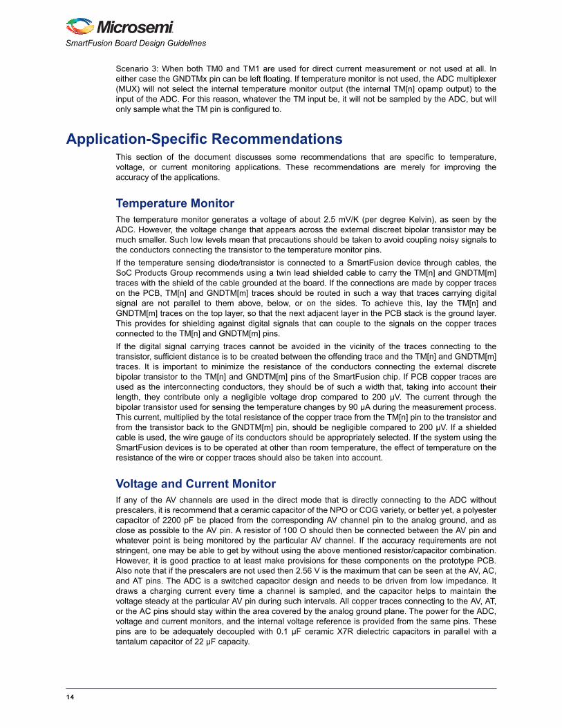
GNDTM[m]The GNDTM[m] pins are the return path for the TM[n] pins that are used in temperature monitorapplications. Each GNDTM pin acts as a return path for one or two TM pins. The GNDTM[m] should notbe connected to ground since there are chances that the temperature monitor accuracy could besensitive to board level noise. There are three different scenarios in which this pin can be used. Thebelow scenarios make use of TM0 and TM1 pins with GNDTM0 as their common return path. Similarconnections can be made for the other temperature monitor pins TM2, TM3, and TM4.
Figure 11 • PU_N Connection to External Switch
EVQ-PAD04MPU_N
1
4
2
3
12
Other Special Function Pins
Scenario 1: When either TM0 or TM1 is used for temperature measurement while the other is used fordirect current measurement or not used at all. In this case the connections are done as shown inFigure 12.
Scenario 2: When both TM0 and TM1 are used for temperature measurement. In this case theconnections are done with the GNDTM0 being connected as a common return path for both TM0 andTM1 as shown in Figure 13.
Figure 12 • TM0 is used for Temperature Measurement
Figure 13 • TM0 and TM1 are used for Temperature Measurement
13
SmartFusion Board Design Guidelines
Scenario 3: When both TM0 and TM1 are used for direct current measurement or not used at all. Ineither case the GNDTMx pin can be left floating. If temperature monitor is not used, the ADC multiplexer(MUX) will not select the internal temperature monitor output (the internal TM[n] opamp output) to theinput of the ADC. For this reason, whatever the TM input be, it will not be sampled by the ADC, but willonly sample what the TM pin is configured to.
Application-Specific RecommendationsThis section of the document discusses some recommendations that are specific to temperature,voltage, or current monitoring applications. These recommendations are merely for improving theaccuracy of the applications.
Temperature MonitorThe temperature monitor generates a voltage of about 2.5 mV/K (per degree Kelvin), as seen by theADC. However, the voltage change that appears across the external discreet bipolar transistor may bemuch smaller. Such low levels mean that precautions should be taken to avoid coupling noisy signals tothe conductors connecting the transistor to the temperature monitor pins.
If the temperature sensing diode/transistor is connected to a SmartFusion device through cables, theSoC Products Group recommends using a twin lead shielded cable to carry the TM[n] and GNDTM[m]traces with the shield of the cable grounded at the board. If the connections are made by copper traceson the PCB, TM[n] and GNDTM[m] traces should be routed in such a way that traces carrying digitalsignal are not parallel to them above, below, or on the sides. To achieve this, lay the TM[n] andGNDTM[m] traces on the top layer, so that the next adjacent layer in the PCB stack is the ground layer.This provides for shielding against digital signals that can couple to the signals on the copper tracesconnected to the TM[n] and GNDTM[m] pins.
If the digital signal carrying traces cannot be avoided in the vicinity of the traces connecting to thetransistor, sufficient distance is to be created between the offending trace and the TM[n] and GNDTM[m]traces. It is important to minimize the resistance of the conductors connecting the external discretebipolar transistor to the TM[n] and GNDTM[m] pins of the SmartFusion chip. If PCB copper traces areused as the interconnecting conductors, they should be of such a width that, taking into account theirlength, they contribute only a negligible voltage drop compared to 200 µV. The current through thebipolar transistor used for sensing the temperature changes by 90 µA during the measurement process.This current, multiplied by the total resistance of the copper trace from the TM[n] pin to the transistor andfrom the transistor back to the GNDTM[m] pin, should be negligible compared to 200 µV. If a shieldedcable is used, the wire gauge of its conductors should be appropriately selected. If the system using theSmartFusion devices is to be operated at other than room temperature, the effect of temperature on theresistance of the wire or copper traces should also be taken into account.
Voltage and Current MonitorIf any of the AV channels are used in the direct mode that is directly connecting to the ADC withoutprescalers, it is recommend that a ceramic capacitor of the NPO or COG variety, or better yet, a polyestercapacitor of 2200 pF be placed from the corresponding AV channel pin to the analog ground, and asclose as possible to the AV pin. A resistor of 100 O should then be connected between the AV pin andwhatever point is being monitored by the particular AV channel. If the accuracy requirements are notstringent, one may be able to get by without using the above mentioned resistor/capacitor combination.However, it is good practice to at least make provisions for these components on the prototype PCB.Also note that if the prescalers are not used then 2.56 V is the maximum that can be seen at the AV, AC,and AT pins. The ADC is a switched capacitor design and needs to be driven from low impedance. Itdraws a charging current every time a channel is sampled, and the capacitor helps to maintain thevoltage steady at the particular AV pin during such intervals. All copper traces connecting to the AV, AT,or the AC pins should stay within the area covered by the analog ground plane. The power for the ADC,voltage and current monitors, and the internal voltage reference is provided from the same pins. Thesepins are to be adequately decoupled with 0.1 µF ceramic X7R dielectric capacitors in parallel with atantalum capacitor of 22 µF capacity.
14
Application-Specific Recommendations
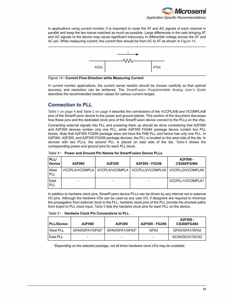
In applications using current monitor, it is important to route the AT and AC signals of each channel inparallel and keep the two traces matched as much as possible. Large differences in the nets bringing ATand AC signals to the device may cause significant inaccuracy in differential voltage across the AT andAC pin. While measuring current, the current flow should be from AC to AT as shown in Figure 14.
In current monitor applications, the current sense resistor should be chosen carefully so that optimalaccuracy and resolution can be achieved. The SmartFusion Programmable Analog User’s Guidedescribes the recommended resistor values for various current ranges.
Connection to PLLTable 1 on page 4 and Table 2 on page 6 describe the connections of the VCCPLA/B and VCOMPLA/Bpins of the SmartFusion device to the power and ground planes. This section of the document discusseshow these pins and the dedicated clock pins of the SmartFusion device connect to the PLLs on the chip.
Connecting external signals into PLL and powering them up should be done considering that A2F060and A2F200 devices contain only one PLL, while A2F500 FG484 package device contain two PLLblocks. Note that A2F500 FG256 package does not have the FAB PLL and hence has only one PLL. InA2F060, A2F200, and A2F500 FG256 package devices, the PLL is located on the west side of the die. Indevices with two PLLs, the second PLL is placed on east side of the die. Table 4 shows thecorresponding power and ground pins for each PLL block.
In addition to hardwire clock pins, SmartFusion device PLLs can be driven by any internal net or externalI/O pins. Although the hardwire I/Os can be used as any user I/O, if designers are required to minimizethe propagation from external clock to the PLL, hardwire clock pins of the PLL provide the shortest pathsfrom board to PLL clock input. Table 5 lists the hardwire clock pins for each PLL on the device.
*Depending on the selected package, not all three hardware clock I/Os may be available.
Figure 14 • Current Flow Direction while Measuring Current
Table 4 • Power and Ground Pin Names for SmartFusion Device PLLs
PLL/Device A2F060 A2F200 A2F500 - FG256
A2F500 - CS288/FG484
WestPLL
VCCPLA/VCOMPLA VCCPLA/VCOMPLA VCCPLL0/VCOMPLA0 VCCPLL0/VCOMPLA0
EastPLL
- - - VCCPLL1/VCOMPLA1
Table 5 • Hardwire Clock Pin Connections to PLL
PLL/Device A2F060 A2F200 A2F500 - FG256A2F500 -
CS288/FG484
West PLL GFA0/GFA1/GFA2* GFA0/GFA1/GFA2* GFA2 GFA0/GFA1/GFA2
East PLL - - - GCA0/GCA1/GCA2
AC[n] AT[n]
i
15
SmartFusion Board Design Guidelines
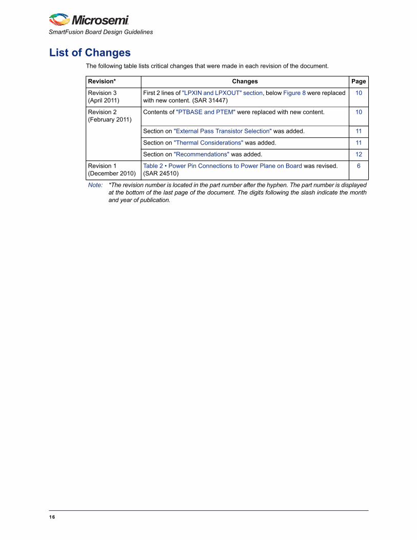
List of ChangesThe following table lists critical changes that were made in each revision of the document.
Revision* Changes Page
Revision 3(April 2011)
First 2 lines of "LPXIN and LPXOUT" section, below Figure 8 were replaced with new content. (SAR 31447)
10
Revision 2(February 2011)
Contents of "PTBASE and PTEM" were replaced with new content. 10
Section on "External Pass Transistor Selection" was added. 11
Section on "Thermal Considerations" was added. 11
Section on "Recommendations" was added. 12
Revision 1(December 2010)
Table 2 • Power Pin Connections to Power Plane on Board was revised. (SAR 24510)
6
Note: *The revision number is located in the part number after the hyphen. The part number is displayedat the bottom of the last page of the document. The digits following the slash indicate the monthand year of publication.
16

51900227-3/4.11
© 2011 Microsemi Corporation. All rights reserved. Microsemi and the Microsemi logo are trademarks of MicrosemiCorporation. All other trademarks and service marks are the property of their respective owners.
Microsemi Corporation (NASDAQ: MSCC) offers the industry’s most comprehensive portfolio ofsemiconductor technology. Committed to solving the most critical system challenges, Microsemi’sproducts include high-performance, high-reliability analog and RF devices, mixed signal integratedcircuits, FPGAs and customizable SoCs, and complete subsystems. Microsemi serves leadingsystem manufacturers around the world in the defense, security, aerospace, enterprise,commercial, and industrial markets. Learn more at www.microsemi.com.
Microsemmi Corporate Headquarters2381 Morse Avenue, Irvine, CA 92614Phone: 949-221-7100·Fax: 949-756-0308www.microsemi.com